JP4493796B2 - Method for forming dielectric film - Google Patents
Method for forming dielectric film Download PDFInfo
- Publication number
- JP4493796B2 JP4493796B2 JP2000095818A JP2000095818A JP4493796B2 JP 4493796 B2 JP4493796 B2 JP 4493796B2 JP 2000095818 A JP2000095818 A JP 2000095818A JP 2000095818 A JP2000095818 A JP 2000095818A JP 4493796 B2 JP4493796 B2 JP 4493796B2
- Authority
- JP
- Japan
- Prior art keywords
- forming
- dielectric film
- film
- gas phase
- molecular compound
- Prior art date
- Legal status (The legal status is an assumption and is not a legal conclusion. Google has not performed a legal analysis and makes no representation as to the accuracy of the status listed.)
- Expired - Fee Related
Links
- 238000000034 method Methods 0.000 title claims description 61
- 239000002052 molecular layer Substances 0.000 claims description 66
- 239000000758 substrate Substances 0.000 claims description 65
- 229910004298 SiO 2 Inorganic materials 0.000 claims description 35
- 150000001875 compounds Chemical class 0.000 claims description 29
- 239000012071 phase Substances 0.000 claims description 27
- 238000005229 chemical vapour deposition Methods 0.000 claims description 15
- 229910003902 SiCl 4 Inorganic materials 0.000 claims description 11
- 239000000203 mixture Substances 0.000 claims description 10
- 239000003989 dielectric material Substances 0.000 claims description 9
- 239000012808 vapor phase Substances 0.000 claims description 9
- 238000000151 deposition Methods 0.000 claims description 8
- 230000003647 oxidation Effects 0.000 claims description 8
- 238000007254 oxidation reaction Methods 0.000 claims description 8
- 230000015572 biosynthetic process Effects 0.000 claims description 7
- 230000001590 oxidative effect Effects 0.000 claims description 7
- 229910052760 oxygen Inorganic materials 0.000 claims description 7
- 239000002994 raw material Substances 0.000 claims description 7
- 229910006501 ZrSiO Inorganic materials 0.000 claims description 6
- 238000006460 hydrolysis reaction Methods 0.000 claims description 6
- 230000007062 hydrolysis Effects 0.000 claims description 4
- 230000003301 hydrolyzing effect Effects 0.000 claims description 4
- 239000002184 metal Substances 0.000 claims description 4
- 229910052751 metal Inorganic materials 0.000 claims description 4
- 229910007926 ZrCl Inorganic materials 0.000 claims description 3
- 229910018072 Al 2 O 3 Inorganic materials 0.000 claims description 2
- 238000010438 heat treatment Methods 0.000 claims 1
- 238000005191 phase separation Methods 0.000 claims 1
- 238000005979 thermal decomposition reaction Methods 0.000 claims 1
- 230000008569 process Effects 0.000 description 28
- 239000007789 gas Substances 0.000 description 21
- 239000004065 semiconductor Substances 0.000 description 14
- 238000006243 chemical reaction Methods 0.000 description 12
- 238000011534 incubation Methods 0.000 description 12
- 229910052814 silicon oxide Inorganic materials 0.000 description 10
- 230000008021 deposition Effects 0.000 description 7
- 238000009792 diffusion process Methods 0.000 description 7
- 239000012159 carrier gas Substances 0.000 description 5
- 238000010586 diagram Methods 0.000 description 5
- 230000000694 effects Effects 0.000 description 5
- 239000002245 particle Substances 0.000 description 4
- QVGXLLKOCUKJST-UHFFFAOYSA-N atomic oxygen Chemical compound [O] QVGXLLKOCUKJST-UHFFFAOYSA-N 0.000 description 3
- 239000001301 oxygen Substances 0.000 description 3
- 229910021420 polycrystalline silicon Inorganic materials 0.000 description 3
- 229920005591 polysilicon Polymers 0.000 description 3
- 230000001681 protective effect Effects 0.000 description 3
- 238000001179 sorption measurement Methods 0.000 description 3
- 238000009826 distribution Methods 0.000 description 2
- 150000002500 ions Chemical class 0.000 description 2
- 238000000678 plasma activation Methods 0.000 description 2
- 238000004335 scaling law Methods 0.000 description 2
- 238000004904 shortening Methods 0.000 description 2
- 229910052710 silicon Inorganic materials 0.000 description 2
- 238000007740 vapor deposition Methods 0.000 description 2
- YZCKVEUIGOORGS-IGMARMGPSA-N Protium Chemical compound [1H] YZCKVEUIGOORGS-IGMARMGPSA-N 0.000 description 1
- 229910004446 Ta2 O5 Inorganic materials 0.000 description 1
- 230000009471 action Effects 0.000 description 1
- 230000004888 barrier function Effects 0.000 description 1
- 230000008859 change Effects 0.000 description 1
- 238000007796 conventional method Methods 0.000 description 1
- 230000007547 defect Effects 0.000 description 1
- 238000002474 experimental method Methods 0.000 description 1
- 239000012535 impurity Substances 0.000 description 1
- 238000010030 laminating Methods 0.000 description 1
- 238000004519 manufacturing process Methods 0.000 description 1
- 239000000463 material Substances 0.000 description 1
- 239000012528 membrane Substances 0.000 description 1
- QJGQUHMNIGDVPM-UHFFFAOYSA-N nitrogen(.) Chemical compound [N] QJGQUHMNIGDVPM-UHFFFAOYSA-N 0.000 description 1
- 230000006911 nucleation Effects 0.000 description 1
- 238000010899 nucleation Methods 0.000 description 1
- 238000004886 process control Methods 0.000 description 1
- 230000003746 surface roughness Effects 0.000 description 1
Images


Classifications
-
- H—ELECTRICITY
- H01—ELECTRIC ELEMENTS
- H01L—SEMICONDUCTOR DEVICES NOT COVERED BY CLASS H10
- H01L21/00—Processes or apparatus adapted for the manufacture or treatment of semiconductor or solid state devices or of parts thereof
- H01L21/02—Manufacture or treatment of semiconductor devices or of parts thereof
- H01L21/02104—Forming layers
- H01L21/02107—Forming insulating materials on a substrate
- H01L21/02225—Forming insulating materials on a substrate characterised by the process for the formation of the insulating layer
- H01L21/0226—Forming insulating materials on a substrate characterised by the process for the formation of the insulating layer formation by a deposition process
- H01L21/02263—Forming insulating materials on a substrate characterised by the process for the formation of the insulating layer formation by a deposition process deposition from the gas or vapour phase
- H01L21/02271—Forming insulating materials on a substrate characterised by the process for the formation of the insulating layer formation by a deposition process deposition from the gas or vapour phase deposition by decomposition or reaction of gaseous or vapour phase compounds, i.e. chemical vapour deposition
-
- C—CHEMISTRY; METALLURGY
- C23—COATING METALLIC MATERIAL; COATING MATERIAL WITH METALLIC MATERIAL; CHEMICAL SURFACE TREATMENT; DIFFUSION TREATMENT OF METALLIC MATERIAL; COATING BY VACUUM EVAPORATION, BY SPUTTERING, BY ION IMPLANTATION OR BY CHEMICAL VAPOUR DEPOSITION, IN GENERAL; INHIBITING CORROSION OF METALLIC MATERIAL OR INCRUSTATION IN GENERAL
- C23C—COATING METALLIC MATERIAL; COATING MATERIAL WITH METALLIC MATERIAL; SURFACE TREATMENT OF METALLIC MATERIAL BY DIFFUSION INTO THE SURFACE, BY CHEMICAL CONVERSION OR SUBSTITUTION; COATING BY VACUUM EVAPORATION, BY SPUTTERING, BY ION IMPLANTATION OR BY CHEMICAL VAPOUR DEPOSITION, IN GENERAL
- C23C16/00—Chemical coating by decomposition of gaseous compounds, without leaving reaction products of surface material in the coating, i.e. chemical vapour deposition [CVD] processes
- C23C16/02—Pretreatment of the material to be coated
- C23C16/0209—Pretreatment of the material to be coated by heating
- C23C16/0218—Pretreatment of the material to be coated by heating in a reactive atmosphere
-
- C—CHEMISTRY; METALLURGY
- C23—COATING METALLIC MATERIAL; COATING MATERIAL WITH METALLIC MATERIAL; CHEMICAL SURFACE TREATMENT; DIFFUSION TREATMENT OF METALLIC MATERIAL; COATING BY VACUUM EVAPORATION, BY SPUTTERING, BY ION IMPLANTATION OR BY CHEMICAL VAPOUR DEPOSITION, IN GENERAL; INHIBITING CORROSION OF METALLIC MATERIAL OR INCRUSTATION IN GENERAL
- C23C—COATING METALLIC MATERIAL; COATING MATERIAL WITH METALLIC MATERIAL; SURFACE TREATMENT OF METALLIC MATERIAL BY DIFFUSION INTO THE SURFACE, BY CHEMICAL CONVERSION OR SUBSTITUTION; COATING BY VACUUM EVAPORATION, BY SPUTTERING, BY ION IMPLANTATION OR BY CHEMICAL VAPOUR DEPOSITION, IN GENERAL
- C23C16/00—Chemical coating by decomposition of gaseous compounds, without leaving reaction products of surface material in the coating, i.e. chemical vapour deposition [CVD] processes
- C23C16/02—Pretreatment of the material to be coated
- C23C16/0227—Pretreatment of the material to be coated by cleaning or etching
- C23C16/0236—Pretreatment of the material to be coated by cleaning or etching by etching with a reactive gas
-
- C—CHEMISTRY; METALLURGY
- C23—COATING METALLIC MATERIAL; COATING MATERIAL WITH METALLIC MATERIAL; CHEMICAL SURFACE TREATMENT; DIFFUSION TREATMENT OF METALLIC MATERIAL; COATING BY VACUUM EVAPORATION, BY SPUTTERING, BY ION IMPLANTATION OR BY CHEMICAL VAPOUR DEPOSITION, IN GENERAL; INHIBITING CORROSION OF METALLIC MATERIAL OR INCRUSTATION IN GENERAL
- C23C—COATING METALLIC MATERIAL; COATING MATERIAL WITH METALLIC MATERIAL; SURFACE TREATMENT OF METALLIC MATERIAL BY DIFFUSION INTO THE SURFACE, BY CHEMICAL CONVERSION OR SUBSTITUTION; COATING BY VACUUM EVAPORATION, BY SPUTTERING, BY ION IMPLANTATION OR BY CHEMICAL VAPOUR DEPOSITION, IN GENERAL
- C23C16/00—Chemical coating by decomposition of gaseous compounds, without leaving reaction products of surface material in the coating, i.e. chemical vapour deposition [CVD] processes
- C23C16/02—Pretreatment of the material to be coated
- C23C16/0272—Deposition of sub-layers, e.g. to promote the adhesion of the main coating
-
- C—CHEMISTRY; METALLURGY
- C23—COATING METALLIC MATERIAL; COATING MATERIAL WITH METALLIC MATERIAL; CHEMICAL SURFACE TREATMENT; DIFFUSION TREATMENT OF METALLIC MATERIAL; COATING BY VACUUM EVAPORATION, BY SPUTTERING, BY ION IMPLANTATION OR BY CHEMICAL VAPOUR DEPOSITION, IN GENERAL; INHIBITING CORROSION OF METALLIC MATERIAL OR INCRUSTATION IN GENERAL
- C23C—COATING METALLIC MATERIAL; COATING MATERIAL WITH METALLIC MATERIAL; SURFACE TREATMENT OF METALLIC MATERIAL BY DIFFUSION INTO THE SURFACE, BY CHEMICAL CONVERSION OR SUBSTITUTION; COATING BY VACUUM EVAPORATION, BY SPUTTERING, BY ION IMPLANTATION OR BY CHEMICAL VAPOUR DEPOSITION, IN GENERAL
- C23C16/00—Chemical coating by decomposition of gaseous compounds, without leaving reaction products of surface material in the coating, i.e. chemical vapour deposition [CVD] processes
- C23C16/22—Chemical coating by decomposition of gaseous compounds, without leaving reaction products of surface material in the coating, i.e. chemical vapour deposition [CVD] processes characterised by the deposition of inorganic material, other than metallic material
- C23C16/30—Deposition of compounds, mixtures or solid solutions, e.g. borides, carbides, nitrides
- C23C16/40—Oxides
- C23C16/401—Oxides containing silicon
-
- C—CHEMISTRY; METALLURGY
- C23—COATING METALLIC MATERIAL; COATING MATERIAL WITH METALLIC MATERIAL; CHEMICAL SURFACE TREATMENT; DIFFUSION TREATMENT OF METALLIC MATERIAL; COATING BY VACUUM EVAPORATION, BY SPUTTERING, BY ION IMPLANTATION OR BY CHEMICAL VAPOUR DEPOSITION, IN GENERAL; INHIBITING CORROSION OF METALLIC MATERIAL OR INCRUSTATION IN GENERAL
- C23C—COATING METALLIC MATERIAL; COATING MATERIAL WITH METALLIC MATERIAL; SURFACE TREATMENT OF METALLIC MATERIAL BY DIFFUSION INTO THE SURFACE, BY CHEMICAL CONVERSION OR SUBSTITUTION; COATING BY VACUUM EVAPORATION, BY SPUTTERING, BY ION IMPLANTATION OR BY CHEMICAL VAPOUR DEPOSITION, IN GENERAL
- C23C16/00—Chemical coating by decomposition of gaseous compounds, without leaving reaction products of surface material in the coating, i.e. chemical vapour deposition [CVD] processes
- C23C16/22—Chemical coating by decomposition of gaseous compounds, without leaving reaction products of surface material in the coating, i.e. chemical vapour deposition [CVD] processes characterised by the deposition of inorganic material, other than metallic material
- C23C16/30—Deposition of compounds, mixtures or solid solutions, e.g. borides, carbides, nitrides
- C23C16/40—Oxides
- C23C16/403—Oxides of aluminium, magnesium or beryllium
-
- C—CHEMISTRY; METALLURGY
- C23—COATING METALLIC MATERIAL; COATING MATERIAL WITH METALLIC MATERIAL; CHEMICAL SURFACE TREATMENT; DIFFUSION TREATMENT OF METALLIC MATERIAL; COATING BY VACUUM EVAPORATION, BY SPUTTERING, BY ION IMPLANTATION OR BY CHEMICAL VAPOUR DEPOSITION, IN GENERAL; INHIBITING CORROSION OF METALLIC MATERIAL OR INCRUSTATION IN GENERAL
- C23C—COATING METALLIC MATERIAL; COATING MATERIAL WITH METALLIC MATERIAL; SURFACE TREATMENT OF METALLIC MATERIAL BY DIFFUSION INTO THE SURFACE, BY CHEMICAL CONVERSION OR SUBSTITUTION; COATING BY VACUUM EVAPORATION, BY SPUTTERING, BY ION IMPLANTATION OR BY CHEMICAL VAPOUR DEPOSITION, IN GENERAL
- C23C16/00—Chemical coating by decomposition of gaseous compounds, without leaving reaction products of surface material in the coating, i.e. chemical vapour deposition [CVD] processes
- C23C16/22—Chemical coating by decomposition of gaseous compounds, without leaving reaction products of surface material in the coating, i.e. chemical vapour deposition [CVD] processes characterised by the deposition of inorganic material, other than metallic material
- C23C16/30—Deposition of compounds, mixtures or solid solutions, e.g. borides, carbides, nitrides
- C23C16/40—Oxides
- C23C16/405—Oxides of refractory metals or yttrium
-
- C—CHEMISTRY; METALLURGY
- C23—COATING METALLIC MATERIAL; COATING MATERIAL WITH METALLIC MATERIAL; CHEMICAL SURFACE TREATMENT; DIFFUSION TREATMENT OF METALLIC MATERIAL; COATING BY VACUUM EVAPORATION, BY SPUTTERING, BY ION IMPLANTATION OR BY CHEMICAL VAPOUR DEPOSITION, IN GENERAL; INHIBITING CORROSION OF METALLIC MATERIAL OR INCRUSTATION IN GENERAL
- C23C—COATING METALLIC MATERIAL; COATING MATERIAL WITH METALLIC MATERIAL; SURFACE TREATMENT OF METALLIC MATERIAL BY DIFFUSION INTO THE SURFACE, BY CHEMICAL CONVERSION OR SUBSTITUTION; COATING BY VACUUM EVAPORATION, BY SPUTTERING, BY ION IMPLANTATION OR BY CHEMICAL VAPOUR DEPOSITION, IN GENERAL
- C23C16/00—Chemical coating by decomposition of gaseous compounds, without leaving reaction products of surface material in the coating, i.e. chemical vapour deposition [CVD] processes
- C23C16/44—Chemical coating by decomposition of gaseous compounds, without leaving reaction products of surface material in the coating, i.e. chemical vapour deposition [CVD] processes characterised by the method of coating
- C23C16/455—Chemical coating by decomposition of gaseous compounds, without leaving reaction products of surface material in the coating, i.e. chemical vapour deposition [CVD] processes characterised by the method of coating characterised by the method used for introducing gases into reaction chamber or for modifying gas flows in reaction chamber
- C23C16/45523—Pulsed gas flow or change of composition over time
- C23C16/45525—Atomic layer deposition [ALD]
-
- H—ELECTRICITY
- H01—ELECTRIC ELEMENTS
- H01L—SEMICONDUCTOR DEVICES NOT COVERED BY CLASS H10
- H01L21/00—Processes or apparatus adapted for the manufacture or treatment of semiconductor or solid state devices or of parts thereof
- H01L21/02—Manufacture or treatment of semiconductor devices or of parts thereof
- H01L21/02104—Forming layers
- H01L21/02107—Forming insulating materials on a substrate
- H01L21/02109—Forming insulating materials on a substrate characterised by the type of layer, e.g. type of material, porous/non-porous, pre-cursors, mixtures or laminates
- H01L21/02112—Forming insulating materials on a substrate characterised by the type of layer, e.g. type of material, porous/non-porous, pre-cursors, mixtures or laminates characterised by the material of the layer
- H01L21/02172—Forming insulating materials on a substrate characterised by the type of layer, e.g. type of material, porous/non-porous, pre-cursors, mixtures or laminates characterised by the material of the layer the material containing at least one metal element, e.g. metal oxides, metal nitrides, metal oxynitrides or metal carbides
- H01L21/02175—Forming insulating materials on a substrate characterised by the type of layer, e.g. type of material, porous/non-porous, pre-cursors, mixtures or laminates characterised by the material of the layer the material containing at least one metal element, e.g. metal oxides, metal nitrides, metal oxynitrides or metal carbides characterised by the metal
- H01L21/02178—Forming insulating materials on a substrate characterised by the type of layer, e.g. type of material, porous/non-porous, pre-cursors, mixtures or laminates characterised by the material of the layer the material containing at least one metal element, e.g. metal oxides, metal nitrides, metal oxynitrides or metal carbides characterised by the metal the material containing aluminium, e.g. Al2O3
-
- H—ELECTRICITY
- H01—ELECTRIC ELEMENTS
- H01L—SEMICONDUCTOR DEVICES NOT COVERED BY CLASS H10
- H01L21/00—Processes or apparatus adapted for the manufacture or treatment of semiconductor or solid state devices or of parts thereof
- H01L21/02—Manufacture or treatment of semiconductor devices or of parts thereof
- H01L21/02104—Forming layers
- H01L21/02107—Forming insulating materials on a substrate
- H01L21/02109—Forming insulating materials on a substrate characterised by the type of layer, e.g. type of material, porous/non-porous, pre-cursors, mixtures or laminates
- H01L21/02112—Forming insulating materials on a substrate characterised by the type of layer, e.g. type of material, porous/non-porous, pre-cursors, mixtures or laminates characterised by the material of the layer
- H01L21/02172—Forming insulating materials on a substrate characterised by the type of layer, e.g. type of material, porous/non-porous, pre-cursors, mixtures or laminates characterised by the material of the layer the material containing at least one metal element, e.g. metal oxides, metal nitrides, metal oxynitrides or metal carbides
- H01L21/02175—Forming insulating materials on a substrate characterised by the type of layer, e.g. type of material, porous/non-porous, pre-cursors, mixtures or laminates characterised by the material of the layer the material containing at least one metal element, e.g. metal oxides, metal nitrides, metal oxynitrides or metal carbides characterised by the metal
- H01L21/02181—Forming insulating materials on a substrate characterised by the type of layer, e.g. type of material, porous/non-porous, pre-cursors, mixtures or laminates characterised by the material of the layer the material containing at least one metal element, e.g. metal oxides, metal nitrides, metal oxynitrides or metal carbides characterised by the metal the material containing hafnium, e.g. HfO2
-
- H—ELECTRICITY
- H01—ELECTRIC ELEMENTS
- H01L—SEMICONDUCTOR DEVICES NOT COVERED BY CLASS H10
- H01L21/00—Processes or apparatus adapted for the manufacture or treatment of semiconductor or solid state devices or of parts thereof
- H01L21/02—Manufacture or treatment of semiconductor devices or of parts thereof
- H01L21/02104—Forming layers
- H01L21/02107—Forming insulating materials on a substrate
- H01L21/02109—Forming insulating materials on a substrate characterised by the type of layer, e.g. type of material, porous/non-porous, pre-cursors, mixtures or laminates
- H01L21/02112—Forming insulating materials on a substrate characterised by the type of layer, e.g. type of material, porous/non-porous, pre-cursors, mixtures or laminates characterised by the material of the layer
- H01L21/02172—Forming insulating materials on a substrate characterised by the type of layer, e.g. type of material, porous/non-porous, pre-cursors, mixtures or laminates characterised by the material of the layer the material containing at least one metal element, e.g. metal oxides, metal nitrides, metal oxynitrides or metal carbides
- H01L21/02175—Forming insulating materials on a substrate characterised by the type of layer, e.g. type of material, porous/non-porous, pre-cursors, mixtures or laminates characterised by the material of the layer the material containing at least one metal element, e.g. metal oxides, metal nitrides, metal oxynitrides or metal carbides characterised by the metal
- H01L21/02183—Forming insulating materials on a substrate characterised by the type of layer, e.g. type of material, porous/non-porous, pre-cursors, mixtures or laminates characterised by the material of the layer the material containing at least one metal element, e.g. metal oxides, metal nitrides, metal oxynitrides or metal carbides characterised by the metal the material containing tantalum, e.g. Ta2O5
-
- H—ELECTRICITY
- H01—ELECTRIC ELEMENTS
- H01L—SEMICONDUCTOR DEVICES NOT COVERED BY CLASS H10
- H01L21/00—Processes or apparatus adapted for the manufacture or treatment of semiconductor or solid state devices or of parts thereof
- H01L21/02—Manufacture or treatment of semiconductor devices or of parts thereof
- H01L21/02104—Forming layers
- H01L21/02107—Forming insulating materials on a substrate
- H01L21/02109—Forming insulating materials on a substrate characterised by the type of layer, e.g. type of material, porous/non-porous, pre-cursors, mixtures or laminates
- H01L21/02112—Forming insulating materials on a substrate characterised by the type of layer, e.g. type of material, porous/non-porous, pre-cursors, mixtures or laminates characterised by the material of the layer
- H01L21/02172—Forming insulating materials on a substrate characterised by the type of layer, e.g. type of material, porous/non-porous, pre-cursors, mixtures or laminates characterised by the material of the layer the material containing at least one metal element, e.g. metal oxides, metal nitrides, metal oxynitrides or metal carbides
- H01L21/02175—Forming insulating materials on a substrate characterised by the type of layer, e.g. type of material, porous/non-porous, pre-cursors, mixtures or laminates characterised by the material of the layer the material containing at least one metal element, e.g. metal oxides, metal nitrides, metal oxynitrides or metal carbides characterised by the metal
- H01L21/02189—Forming insulating materials on a substrate characterised by the type of layer, e.g. type of material, porous/non-porous, pre-cursors, mixtures or laminates characterised by the material of the layer the material containing at least one metal element, e.g. metal oxides, metal nitrides, metal oxynitrides or metal carbides characterised by the metal the material containing zirconium, e.g. ZrO2
-
- H—ELECTRICITY
- H01—ELECTRIC ELEMENTS
- H01L—SEMICONDUCTOR DEVICES NOT COVERED BY CLASS H10
- H01L21/00—Processes or apparatus adapted for the manufacture or treatment of semiconductor or solid state devices or of parts thereof
- H01L21/02—Manufacture or treatment of semiconductor devices or of parts thereof
- H01L21/02104—Forming layers
- H01L21/02107—Forming insulating materials on a substrate
- H01L21/02109—Forming insulating materials on a substrate characterised by the type of layer, e.g. type of material, porous/non-porous, pre-cursors, mixtures or laminates
- H01L21/022—Forming insulating materials on a substrate characterised by the type of layer, e.g. type of material, porous/non-porous, pre-cursors, mixtures or laminates the layer being a laminate, i.e. composed of sublayers, e.g. stacks of alternating high-k metal oxides
-
- H—ELECTRICITY
- H01—ELECTRIC ELEMENTS
- H01L—SEMICONDUCTOR DEVICES NOT COVERED BY CLASS H10
- H01L21/00—Processes or apparatus adapted for the manufacture or treatment of semiconductor or solid state devices or of parts thereof
- H01L21/02—Manufacture or treatment of semiconductor devices or of parts thereof
- H01L21/04—Manufacture or treatment of semiconductor devices or of parts thereof the devices having potential barriers, e.g. a PN junction, depletion layer or carrier concentration layer
- H01L21/18—Manufacture or treatment of semiconductor devices or of parts thereof the devices having potential barriers, e.g. a PN junction, depletion layer or carrier concentration layer the devices having semiconductor bodies comprising elements of Group IV of the Periodic Table or AIIIBV compounds with or without impurities, e.g. doping materials
- H01L21/28—Manufacture of electrodes on semiconductor bodies using processes or apparatus not provided for in groups H01L21/20 - H01L21/268
- H01L21/28008—Making conductor-insulator-semiconductor electrodes
- H01L21/28017—Making conductor-insulator-semiconductor electrodes the insulator being formed after the semiconductor body, the semiconductor being silicon
- H01L21/28158—Making the insulator
- H01L21/28167—Making the insulator on single crystalline silicon, e.g. using a liquid, i.e. chemical oxidation
- H01L21/28185—Making the insulator on single crystalline silicon, e.g. using a liquid, i.e. chemical oxidation with a treatment, e.g. annealing, after the formation of the gate insulator and before the formation of the definitive gate conductor
-
- H—ELECTRICITY
- H01—ELECTRIC ELEMENTS
- H01L—SEMICONDUCTOR DEVICES NOT COVERED BY CLASS H10
- H01L21/00—Processes or apparatus adapted for the manufacture or treatment of semiconductor or solid state devices or of parts thereof
- H01L21/02—Manufacture or treatment of semiconductor devices or of parts thereof
- H01L21/04—Manufacture or treatment of semiconductor devices or of parts thereof the devices having potential barriers, e.g. a PN junction, depletion layer or carrier concentration layer
- H01L21/18—Manufacture or treatment of semiconductor devices or of parts thereof the devices having potential barriers, e.g. a PN junction, depletion layer or carrier concentration layer the devices having semiconductor bodies comprising elements of Group IV of the Periodic Table or AIIIBV compounds with or without impurities, e.g. doping materials
- H01L21/28—Manufacture of electrodes on semiconductor bodies using processes or apparatus not provided for in groups H01L21/20 - H01L21/268
- H01L21/28008—Making conductor-insulator-semiconductor electrodes
- H01L21/28017—Making conductor-insulator-semiconductor electrodes the insulator being formed after the semiconductor body, the semiconductor being silicon
- H01L21/28158—Making the insulator
- H01L21/28167—Making the insulator on single crystalline silicon, e.g. using a liquid, i.e. chemical oxidation
- H01L21/28194—Making the insulator on single crystalline silicon, e.g. using a liquid, i.e. chemical oxidation by deposition, e.g. evaporation, ALD, CVD, sputtering, laser deposition
-
- H—ELECTRICITY
- H01—ELECTRIC ELEMENTS
- H01L—SEMICONDUCTOR DEVICES NOT COVERED BY CLASS H10
- H01L21/00—Processes or apparatus adapted for the manufacture or treatment of semiconductor or solid state devices or of parts thereof
- H01L21/02—Manufacture or treatment of semiconductor devices or of parts thereof
- H01L21/04—Manufacture or treatment of semiconductor devices or of parts thereof the devices having potential barriers, e.g. a PN junction, depletion layer or carrier concentration layer
- H01L21/18—Manufacture or treatment of semiconductor devices or of parts thereof the devices having potential barriers, e.g. a PN junction, depletion layer or carrier concentration layer the devices having semiconductor bodies comprising elements of Group IV of the Periodic Table or AIIIBV compounds with or without impurities, e.g. doping materials
- H01L21/30—Treatment of semiconductor bodies using processes or apparatus not provided for in groups H01L21/20 - H01L21/26
- H01L21/31—Treatment of semiconductor bodies using processes or apparatus not provided for in groups H01L21/20 - H01L21/26 to form insulating layers thereon, e.g. for masking or by using photolithographic techniques; After treatment of these layers; Selection of materials for these layers
- H01L21/314—Inorganic layers
- H01L21/316—Inorganic layers composed of oxides or glassy oxides or oxide based glass
- H01L21/31604—Deposition from a gas or vapour
-
- H—ELECTRICITY
- H01—ELECTRIC ELEMENTS
- H01L—SEMICONDUCTOR DEVICES NOT COVERED BY CLASS H10
- H01L29/00—Semiconductor devices specially adapted for rectifying, amplifying, oscillating or switching and having potential barriers; Capacitors or resistors having potential barriers, e.g. a PN-junction depletion layer or carrier concentration layer; Details of semiconductor bodies or of electrodes thereof ; Multistep manufacturing processes therefor
- H01L29/40—Electrodes ; Multistep manufacturing processes therefor
- H01L29/43—Electrodes ; Multistep manufacturing processes therefor characterised by the materials of which they are formed
- H01L29/49—Metal-insulator-semiconductor electrodes, e.g. gates of MOSFET
- H01L29/51—Insulating materials associated therewith
- H01L29/511—Insulating materials associated therewith with a compositional variation, e.g. multilayer structures
- H01L29/513—Insulating materials associated therewith with a compositional variation, e.g. multilayer structures the variation being perpendicular to the channel plane
-
- H—ELECTRICITY
- H01—ELECTRIC ELEMENTS
- H01L—SEMICONDUCTOR DEVICES NOT COVERED BY CLASS H10
- H01L29/00—Semiconductor devices specially adapted for rectifying, amplifying, oscillating or switching and having potential barriers; Capacitors or resistors having potential barriers, e.g. a PN-junction depletion layer or carrier concentration layer; Details of semiconductor bodies or of electrodes thereof ; Multistep manufacturing processes therefor
- H01L29/40—Electrodes ; Multistep manufacturing processes therefor
- H01L29/43—Electrodes ; Multistep manufacturing processes therefor characterised by the materials of which they are formed
- H01L29/49—Metal-insulator-semiconductor electrodes, e.g. gates of MOSFET
- H01L29/51—Insulating materials associated therewith
- H01L29/517—Insulating materials associated therewith the insulating material comprising a metallic compound, e.g. metal oxide, metal silicate
-
- H—ELECTRICITY
- H01—ELECTRIC ELEMENTS
- H01L—SEMICONDUCTOR DEVICES NOT COVERED BY CLASS H10
- H01L29/00—Semiconductor devices specially adapted for rectifying, amplifying, oscillating or switching and having potential barriers; Capacitors or resistors having potential barriers, e.g. a PN-junction depletion layer or carrier concentration layer; Details of semiconductor bodies or of electrodes thereof ; Multistep manufacturing processes therefor
- H01L29/40—Electrodes ; Multistep manufacturing processes therefor
- H01L29/43—Electrodes ; Multistep manufacturing processes therefor characterised by the materials of which they are formed
- H01L29/49—Metal-insulator-semiconductor electrodes, e.g. gates of MOSFET
- H01L29/51—Insulating materials associated therewith
- H01L29/518—Insulating materials associated therewith the insulating material containing nitrogen, e.g. nitride, oxynitride, nitrogen-doped material
-
- H—ELECTRICITY
- H01—ELECTRIC ELEMENTS
- H01L—SEMICONDUCTOR DEVICES NOT COVERED BY CLASS H10
- H01L21/00—Processes or apparatus adapted for the manufacture or treatment of semiconductor or solid state devices or of parts thereof
- H01L21/02—Manufacture or treatment of semiconductor devices or of parts thereof
- H01L21/02104—Forming layers
- H01L21/02107—Forming insulating materials on a substrate
- H01L21/02109—Forming insulating materials on a substrate characterised by the type of layer, e.g. type of material, porous/non-porous, pre-cursors, mixtures or laminates
- H01L21/02112—Forming insulating materials on a substrate characterised by the type of layer, e.g. type of material, porous/non-porous, pre-cursors, mixtures or laminates characterised by the material of the layer
- H01L21/02123—Forming insulating materials on a substrate characterised by the type of layer, e.g. type of material, porous/non-porous, pre-cursors, mixtures or laminates characterised by the material of the layer the material containing silicon
- H01L21/02142—Forming insulating materials on a substrate characterised by the type of layer, e.g. type of material, porous/non-porous, pre-cursors, mixtures or laminates characterised by the material of the layer the material containing silicon the material containing silicon and at least one metal element, e.g. metal silicate based insulators or metal silicon oxynitrides
- H01L21/02148—Forming insulating materials on a substrate characterised by the type of layer, e.g. type of material, porous/non-porous, pre-cursors, mixtures or laminates characterised by the material of the layer the material containing silicon the material containing silicon and at least one metal element, e.g. metal silicate based insulators or metal silicon oxynitrides the material containing hafnium, e.g. HfSiOx or HfSiON
-
- H—ELECTRICITY
- H01—ELECTRIC ELEMENTS
- H01L—SEMICONDUCTOR DEVICES NOT COVERED BY CLASS H10
- H01L21/00—Processes or apparatus adapted for the manufacture or treatment of semiconductor or solid state devices or of parts thereof
- H01L21/02—Manufacture or treatment of semiconductor devices or of parts thereof
- H01L21/02104—Forming layers
- H01L21/02107—Forming insulating materials on a substrate
- H01L21/02109—Forming insulating materials on a substrate characterised by the type of layer, e.g. type of material, porous/non-porous, pre-cursors, mixtures or laminates
- H01L21/02112—Forming insulating materials on a substrate characterised by the type of layer, e.g. type of material, porous/non-porous, pre-cursors, mixtures or laminates characterised by the material of the layer
- H01L21/02123—Forming insulating materials on a substrate characterised by the type of layer, e.g. type of material, porous/non-porous, pre-cursors, mixtures or laminates characterised by the material of the layer the material containing silicon
- H01L21/02164—Forming insulating materials on a substrate characterised by the type of layer, e.g. type of material, porous/non-porous, pre-cursors, mixtures or laminates characterised by the material of the layer the material containing silicon the material being a silicon oxide, e.g. SiO2
-
- H—ELECTRICITY
- H01—ELECTRIC ELEMENTS
- H01L—SEMICONDUCTOR DEVICES NOT COVERED BY CLASS H10
- H01L21/00—Processes or apparatus adapted for the manufacture or treatment of semiconductor or solid state devices or of parts thereof
- H01L21/02—Manufacture or treatment of semiconductor devices or of parts thereof
- H01L21/02104—Forming layers
- H01L21/02107—Forming insulating materials on a substrate
- H01L21/02109—Forming insulating materials on a substrate characterised by the type of layer, e.g. type of material, porous/non-porous, pre-cursors, mixtures or laminates
- H01L21/02112—Forming insulating materials on a substrate characterised by the type of layer, e.g. type of material, porous/non-porous, pre-cursors, mixtures or laminates characterised by the material of the layer
- H01L21/02172—Forming insulating materials on a substrate characterised by the type of layer, e.g. type of material, porous/non-porous, pre-cursors, mixtures or laminates characterised by the material of the layer the material containing at least one metal element, e.g. metal oxides, metal nitrides, metal oxynitrides or metal carbides
- H01L21/02175—Forming insulating materials on a substrate characterised by the type of layer, e.g. type of material, porous/non-porous, pre-cursors, mixtures or laminates characterised by the material of the layer the material containing at least one metal element, e.g. metal oxides, metal nitrides, metal oxynitrides or metal carbides characterised by the metal
- H01L21/02194—Forming insulating materials on a substrate characterised by the type of layer, e.g. type of material, porous/non-porous, pre-cursors, mixtures or laminates characterised by the material of the layer the material containing at least one metal element, e.g. metal oxides, metal nitrides, metal oxynitrides or metal carbides characterised by the metal the material containing more than one metal element
-
- H—ELECTRICITY
- H01—ELECTRIC ELEMENTS
- H01L—SEMICONDUCTOR DEVICES NOT COVERED BY CLASS H10
- H01L21/00—Processes or apparatus adapted for the manufacture or treatment of semiconductor or solid state devices or of parts thereof
- H01L21/02—Manufacture or treatment of semiconductor devices or of parts thereof
- H01L21/02104—Forming layers
- H01L21/02107—Forming insulating materials on a substrate
- H01L21/02225—Forming insulating materials on a substrate characterised by the process for the formation of the insulating layer
- H01L21/02227—Forming insulating materials on a substrate characterised by the process for the formation of the insulating layer formation by a process other than a deposition process
- H01L21/0223—Forming insulating materials on a substrate characterised by the process for the formation of the insulating layer formation by a process other than a deposition process formation by oxidation, e.g. oxidation of the substrate
- H01L21/02233—Forming insulating materials on a substrate characterised by the process for the formation of the insulating layer formation by a process other than a deposition process formation by oxidation, e.g. oxidation of the substrate of the semiconductor substrate or a semiconductor layer
- H01L21/02236—Forming insulating materials on a substrate characterised by the process for the formation of the insulating layer formation by a process other than a deposition process formation by oxidation, e.g. oxidation of the substrate of the semiconductor substrate or a semiconductor layer group IV semiconductor
- H01L21/02238—Forming insulating materials on a substrate characterised by the process for the formation of the insulating layer formation by a process other than a deposition process formation by oxidation, e.g. oxidation of the substrate of the semiconductor substrate or a semiconductor layer group IV semiconductor silicon in uncombined form, i.e. pure silicon
-
- H—ELECTRICITY
- H01—ELECTRIC ELEMENTS
- H01L—SEMICONDUCTOR DEVICES NOT COVERED BY CLASS H10
- H01L21/00—Processes or apparatus adapted for the manufacture or treatment of semiconductor or solid state devices or of parts thereof
- H01L21/02—Manufacture or treatment of semiconductor devices or of parts thereof
- H01L21/02104—Forming layers
- H01L21/02107—Forming insulating materials on a substrate
- H01L21/02225—Forming insulating materials on a substrate characterised by the process for the formation of the insulating layer
- H01L21/0226—Forming insulating materials on a substrate characterised by the process for the formation of the insulating layer formation by a deposition process
- H01L21/02263—Forming insulating materials on a substrate characterised by the process for the formation of the insulating layer formation by a deposition process deposition from the gas or vapour phase
- H01L21/02271—Forming insulating materials on a substrate characterised by the process for the formation of the insulating layer formation by a deposition process deposition from the gas or vapour phase deposition by decomposition or reaction of gaseous or vapour phase compounds, i.e. chemical vapour deposition
- H01L21/0228—Forming insulating materials on a substrate characterised by the process for the formation of the insulating layer formation by a deposition process deposition from the gas or vapour phase deposition by decomposition or reaction of gaseous or vapour phase compounds, i.e. chemical vapour deposition deposition by cyclic CVD, e.g. ALD, ALE, pulsed CVD
-
- H—ELECTRICITY
- H01—ELECTRIC ELEMENTS
- H01L—SEMICONDUCTOR DEVICES NOT COVERED BY CLASS H10
- H01L21/00—Processes or apparatus adapted for the manufacture or treatment of semiconductor or solid state devices or of parts thereof
- H01L21/02—Manufacture or treatment of semiconductor devices or of parts thereof
- H01L21/04—Manufacture or treatment of semiconductor devices or of parts thereof the devices having potential barriers, e.g. a PN junction, depletion layer or carrier concentration layer
- H01L21/18—Manufacture or treatment of semiconductor devices or of parts thereof the devices having potential barriers, e.g. a PN junction, depletion layer or carrier concentration layer the devices having semiconductor bodies comprising elements of Group IV of the Periodic Table or AIIIBV compounds with or without impurities, e.g. doping materials
- H01L21/30—Treatment of semiconductor bodies using processes or apparatus not provided for in groups H01L21/20 - H01L21/26
- H01L21/31—Treatment of semiconductor bodies using processes or apparatus not provided for in groups H01L21/20 - H01L21/26 to form insulating layers thereon, e.g. for masking or by using photolithographic techniques; After treatment of these layers; Selection of materials for these layers
- H01L21/314—Inorganic layers
- H01L21/316—Inorganic layers composed of oxides or glassy oxides or oxide based glass
- H01L21/3165—Inorganic layers composed of oxides or glassy oxides or oxide based glass formed by oxidation
- H01L21/31683—Inorganic layers composed of oxides or glassy oxides or oxide based glass formed by oxidation of metallic layers, e.g. Al deposited on the body, e.g. formation of multi-layer insulating structures
-
- H—ELECTRICITY
- H01—ELECTRIC ELEMENTS
- H01L—SEMICONDUCTOR DEVICES NOT COVERED BY CLASS H10
- H01L28/00—Passive two-terminal components without a potential-jump or surface barrier for integrated circuits; Details thereof; Multistep manufacturing processes therefor
- H01L28/40—Capacitors
- H01L28/55—Capacitors with a dielectric comprising a perovskite structure material
- H01L28/56—Capacitors with a dielectric comprising a perovskite structure material the dielectric comprising two or more layers, e.g. comprising buffer layers, seed layers, gradient layers
Landscapes
- Chemical & Material Sciences (AREA)
- Engineering & Computer Science (AREA)
- Power Engineering (AREA)
- Microelectronics & Electronic Packaging (AREA)
- Condensed Matter Physics & Semiconductors (AREA)
- Computer Hardware Design (AREA)
- General Physics & Mathematics (AREA)
- Physics & Mathematics (AREA)
- Chemical Kinetics & Catalysis (AREA)
- General Chemical & Material Sciences (AREA)
- Manufacturing & Machinery (AREA)
- Mechanical Engineering (AREA)
- Organic Chemistry (AREA)
- Materials Engineering (AREA)
- Metallurgy (AREA)
- Inorganic Chemistry (AREA)
- Crystallography & Structural Chemistry (AREA)
- Ceramic Engineering (AREA)
- Formation Of Insulating Films (AREA)
- Chemical Vapour Deposition (AREA)
- Insulated Gate Type Field-Effect Transistor (AREA)
Description
【0001】
【発明の属する技術分野】
本発明は半導体装置に係り、特に高誘電体膜を有する、超微細化高速半導体装置の製造方法に関する。
【0002】
今日の超高速高速半導体装置では、微細化プロセスの進歩とともに、0.1μm以下のゲート長が可能になりつつある。一般に微細化とともに半導体装置の動作速度は向上するが、このように非常に微細化された半導体装置では、ゲート絶縁膜の膜厚を、微細化によるゲート長の短縮に伴って、スケーリング則に従って減少させる必要がある。
【0003】
【従来の技術】
しかしゲート長が0.1μm以下になると、ゲート絶縁膜の厚さも、SiO2を使った場合、1〜2nm、あるいはそれ以下に設定する必要があるが、このように非常に薄いゲート絶縁膜ではトンネル電流が増大し、その結果ゲートリーク電流が増大する問題を回避することができない。このため、例えば特開平11−87341号公報に記載されているように、Si基板表面に非常に薄いSiN膜を、前記Si基板表面にSiを含む気相原料を吸着させ、ついでこれにNのラジカルを含む雰囲気を作用させることにより形成することが記載されている。しかし、SiN膜の比誘電率はSiO2膜の比誘電率よりは大きいものの、8程度でしかなく、このためSiN膜を使った場合には、スケーリング則による微細化の要請を満足し、しかもトンネル電流を効果的に遮断できるような実質的な膜厚にゲート絶縁膜を形成することはできない。また、前記特開平11−87341号公報に記載の方法では、Nのラジカルを発生させるためにプラズマを発生させる必要があるが、プラズマ発生源の近傍において基板表面を処理すると、プラズマに起因する電子やイオンなどの荷電粒子がSiN膜中に取り込まれて準位を形成するため、得られるSiN膜のリーク電流特性およびCV特性が劣化してしまう。一方、この問題を回避しようとしてプラズマ発生源を前記基板から離れた位置に設けると,必要なNラジカルの量が大きく減少してしまい、Nの吸着を行うことが難しくなる。
【0004】
このような事情で従来より、比誘電率がSiO2膜のものよりもはるかに大きく、このため実際の膜厚が大きくてもSiO2膜に換算した場合の膜厚が小さいTa2O5のような高誘電体材料をゲート絶縁膜に対して適用することが提案されている。このようなTa2O5などの高誘電体材料を使うことにより、ゲート長が0.1μm以下と、非常に短い超高速半導体装置においても10μm程度の膜厚のゲート絶縁膜を使うことができ、トンネル効果によるゲートリーク電流を抑制することができる。
【0005】
従来より、Ta2O5膜はTa(OC2H5)5およびO2を気相原料としたCVD法により形成できることが知られている。典型的な場合、CVDプロセスは減圧環境下、約480°C、あるいはそれ以上の温度で実行される。このようにして形成されたTa2O5膜は、さらに酸素雰囲気中において熱処理され、その結果、膜中の酸素欠損が解消され、また膜自体が結晶化する。このようにして結晶化されたTa2O5膜は大きな比誘電率を示す。
【0006】
【発明が解決しようとする課題】
一方、Ta2O5等の高誘電体膜をCVD法によりSi基板上に成長させる場合、核生成過程に関連して、CVDプロセスを開始しても直ちには高誘電体膜の堆積は始まらず、あるインキュベーション時間が経過した後で初めて膜の堆積が始まることが知られている。
【0007】
本発明の基礎となる実験において、本発明の発明者は、このインキュベーション時間が前記高誘電体膜を堆積する下地の性質によって変化することを見出した。例えば、下地が酸化膜を除去された清浄なSi基板であれば、インキュベーション時間はわずかであるが、Si基板の表面にSiO2膜あるいはSiN膜、あるいはSiON膜が存在していると、インキュベーション時間は増大する。また、インキュベーション時間は、かかるSiO2膜、SiN膜あるいはSiON膜の膜厚にも依存することが見出された。このことは、SiO2膜、SiN膜あるいはSiON膜上に形成される高誘電体膜の膜厚が、下地膜の膜厚の変動を受け、その結果、下地膜の膜厚変動が増幅される傾向があることを意味する。また、このようにCVD法により形成される高誘電体膜の膜厚が下地の影響を受けるということは、ゲート絶縁膜等に使われる高誘電体膜の膜質が、不均一になりやすいことを意味している。
【0008】
このような高誘電体膜中における膜質の不均一を抑制するには、インキュベーション時間を可能な限り減少させるのが望ましい。
【0009】
さらに、かかる高誘電体膜をゲート絶縁膜に使った半導体装置では、高誘電体膜を直接にSi基板上に形成した方が、絶縁膜のSiO2換算実効膜厚を減少させるためには好ましいものの、ゲートチャネル中のキャリアモビリティーを向上させる観点からは、高誘電体ゲート酸化膜とSi基板との間に、きわめて薄い酸化膜を介在させるのが好ましい。その際、前記高誘電体膜を使うことによる効果を最大化するためには、かかる高誘電体膜の膜質、特に組成を、膜厚方向に変化させることのできる技術が必要になる。前記酸化膜の厚さが厚い場合、あるいは前記高誘電体膜中に実質的な厚さにわたり、Siに富む領域が形成されている場合、高い誘電率を特徴とする高誘電体膜の効果は実質的に減少してしまう。
【0010】
そこで、本発明は上記の課題を解決した、新規で有用な誘電体膜の形成方法を提供することを具体的な課題とする。
【0011】
本発明のより具体的な課題は、気相堆積法による誘電体膜の形成方法において、前記誘電体膜への荷電粒子によるダメージの問題を発生させることなく、前記誘電体膜堆積の際のインキュベーション時間を最小にし、また表面ラフネスを低減することにある。
【0012】
本発明の他の課題は、気相堆積法による誘電体膜の形成方法において、前記誘電体膜への荷電粒子によるダメージの問題を発生させることなく、前記誘電体膜の膜厚方向における組成分布を自在に制御できる方法を提供することにある。
【0013】
【課題を解決するための手段】
本発明は、上記の課題を、
Si基板上への誘電体膜の形成方法において、
前記Si基板上に絶縁性層を形成する工程と、
前記絶縁性層上に少なくとも1回、金属元素の気相分子化合物を実質的に一様に吸着させ、前記絶縁性層上を前記気相分子化合物により覆う工程と、
前記絶縁層を覆う前記気相分子化合物を酸化雰囲気中で分解し、前記絶縁層上に前記金属元素を含む誘電体材料の分子層を形成する工程と、を含み、
前記気相分子化合物を分解させる工程の後、前記誘電体の分子層上に高誘電体膜をCVD法により形成する工程を含むことを特徴とする誘電体膜の形成方法により、解決する。
【0014】
【発明の実施の形態】
[第1実施例]
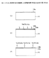
図1(A)〜(C)は、本発明の第1実施例による、Ta2O5膜の形成方法を示す。
【0015】
図1(A)を参照するに、Si基板11は133〜399Pa(1〜3Torr)の内圧に減圧された反応容器(図示せず)中に室温よりも低い温度で保持されており、この状態で前記反応容器中に、N2とH2の混合ガスのプラズマ活性化により形成した窒素ラジカルN*と水素ラジカルH*を、NF3ガスと共に供給することにより、前記Si基板11表面の酸化膜11aを除去する。かかる酸化膜除去工程を低温で行うことにより、前記Si基板11表面には、図1(B)に示すように、前記酸化膜11aの除去と同時に、N−O−Si−Hの組成を有する保護膜11bが形成される。典型的にはH2,NF3およびN2ガスを、それぞれ10sccm,30sccmおよび100sccmの流量で供給し、H2ガスとN2ガスのプラズマ活性化を50Wのプラズマ電力により行う。図1(A)の酸化膜除去処理は3分間程度で十分である。
【0016】
このようにして形成された保護膜11bは揮発性の膜であり、図1(C)の工程において前記Si基板11を前記反応容器中において引き続き真空中、約120°Cの温度で熱処理することにより容易に昇華・除去され、その結果Si基板11においては、新鮮なSi表面11cが露出される。
【0017】
次に図2(D)の工程において、前記反応容器の内圧を1.33〜13.3Pa(0.01〜0.1Torr)に、また基板温度を200〜350°Cに設定し、図1(C)の工程に連続して前記反応容器中にSiCl4ガスを流量が約50sccmのHeキャリアガスと共に0.1〜5mg/minの割合で導入し、前記Si基板表面11cにSiCl4分子を吸着させる。さらに、前記反応容器中にH2Oを前記Heキャリアガスと共に約1sccmの流量で導入し、前記Si基板表面11cに吸着しているSiCl4分子を加水分解する。その結果、前記Si基板11の表面に非常には薄い、典型的には1〜数分子層のSiO2を含むSiO2分子層12aが形成される。図1(D)の工程では、必要に応じて前記SiCl4ガスの導入工程および吸着されたSiCl4分子の加水分解工程を繰り返すことにより、前記SiO2分子層12aを所望の厚さに形成することも可能である。また、図1(D)の工程において前記Si基板11の表面11cに吸着したSiCl4分子をNH3ガスにより処理することにより、SiN分子層を、前記SiO2分子層12aの代わりに形成することもできる。また、前記SiO2分子層とSiN分子層とを適宜積層することにより、前記SiO2分子層12aのかわりにSiON分子層を形成することもできる。また、通常の熱酸化によるSiO2膜も、プロセス制御に関連して豊富なデータが利用できるため、実用上、使用可能である。
【0018】
次に図2(E)の工程において、基板温度を350°C以下、好ましくは約300°C以下、より好ましくは約280°Cに設定し、内圧を前と同じく0.01〜0.1Torrに設定された前記反応容器中にTa(OC2H5)O5ガスとO2ガスとを、Heキャリアガスと共に、それぞれ約5mg/minおよび100sccmの流量で1分間程度供給する。Heキャリアガスの流量は、約100sccmに設定する。その結果、図2(F)に示すように、前記SiO2膜12a上に前記Ta(OC2H5)O5分子が吸着され、Ta(OC2H5)O5吸着分子層12bが前記SiO2分子層12a上に形成される。
【0019】
さらに図3(G)の工程において前記基板温度をO2などの酸化雰囲気中において約350°Cに上昇させ、前記吸着されたTa(OC2H5)O5分子を酸化または加水分解し、前記吸着分子層12bをTa2O5分子層12cに変換する。
【0020】
さらに図3(H)の工程において、基板温度を510°Cに、また前記反応容器の内圧を13.3〜1330Pa(0.1〜10Torr)に設定し、前記反応容器中にTa(OC2H5)O5ガスとO2ガスとを、Heキャリアガスと共に供給し、前記Ta2O5分子層12c上に、通常のCVDプロセスによりTa2O5膜13を所望の厚さ、例えば4〜5nmの厚さに形成する。
【0021】
さらに、図示は省略するが、このようにして形成されたTa2O5膜13に対してO2雰囲気中にて熱処理を施すことにより、膜13中の酸素欠損が補償され、また膜13が結晶化する。このようにして結晶化されたTa2O5膜13は、大きな比誘電率を示す。また、前記Si基板11とTa2O5膜13との界面には前記SiO2分子層12aが形成されているため、Si基板上に形成された素子においてゲートチャネルの大きなキャリアモビリティが保証される。すなわち、このようにして形成された半導体装置は、非常に高速に動作する。
【0022】
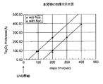
図4は、先の図3(H)のCVD工程における堆積時間と、その結果堆積したTa2O5膜13との関係を、従来のTa2 O5 膜のCVD工程の場合と比較して示す。ただし、前記堆積時間は、CVD工程の開始時点から測っている。図4中、◆は本実施例によるTa2O5膜13の堆積を、一方▲は従来のCVD工程におけるTa2O5膜の堆積を示す。ただし▲で示す従来の場合には、図2(D)において前記SiO2分子層12a上にTa2O5膜をCVD法により、直接に堆積させている。
【0023】
図4を参照するに、従来のCVD工程では、CVDプロセスを開始してから実際にTa2O5膜の堆積が生じるまでに、約140秒間のインキュベーション時間が必要であるのに対し、本実施例による工程では、CVDプロセスを開始してからわずか40秒後にはTa2O5膜の堆積が始まっている。すなわち、本実施例の構成により、Ta2O5膜をCVD法により形成する際のインキュベーション時間を実質的に減少させることが可能である。
【0024】
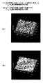
図5(A),(B)は、従来のCVD工程により、Si基板11表面を覆うSiON膜上に形成したTa2O5膜の表面構造をAFMにより観察した結果を示す。ただし、図5(A)では、前記Ta2O5膜を基板温度510°CでのCVD法により、一方図5(B)では、前記Ta2O5膜を、基板温度480°CでのCVD法により、形成している。
【0025】
図5(A),(B)を参照するに、このようにして形成されたCVD−Ta2O5膜は、下地のSiON膜の膜厚変動を反映して、非常に大きな膜厚の変動を示すことがわかる。換言すると、従来のCVD−Ta2O5膜では、下地膜の膜厚変動が増幅され、その結果得られるTa2O5膜の膜厚が不均一になってしまう。
【0026】
これに対し、図6(A)は、前記図1(A)〜図3(G)の本実施例による工程により形成されたTa2O5 膜の表面構造を示す。ただし、図6(A)では、前記SiO2分子層12aの代わりに、SiON分子層を使っている。一方図6(B)は、図1(C)の構造上に、すなわち前記露出されたSi基板表面11c上に、直接にTa2O5膜のCVD法による堆積を行った場合のTa2O5膜の表面構造を示す。図6(A),(B)のいずれの場合にも、前記Ta2O5膜の表面構造はAFM観察により求めている。
【0027】
図6(A)を参照するに、本実施例による工程を採用することにより、CVD法により形成されるTa2O5膜表面の凹凸が実質的に減少し、Si基板上に直接に形成した場合に近い状態になることがわかる。これは先に図4で説明した、下地のSiON膜上にTaの気相分子化合物Ta(OC2H5)5を吸着させ、これを酸化させてTa2O5分子層12cを形成し、かかるTa2O5分子層12c上にTa2O5膜13をCVD法により形成した場合に得られるインキュベーション時間の短縮の結果を反映しているものと考えられる。すなわち、インキュベーション時間が短縮することにより、下地膜の膜質によるインキュベーション時間の変動が抑制され、その結果、CVD法により堆積されるTa2O5膜13の膜厚変動が抑制される。
【0028】
なお、本実施例において使用可能なTa2O5分子層12c形成時に使われる気相分子化合物は先に説明したTa(OC2H5)5に限定されるものではなく、例えばTaCl5を使うことも可能である。この場合にも、前記TaCl5分子の吸着工程は、反応容器の内圧を0.133〜13.3Pa(0.001〜0.1Torr)程度に設定し、200〜300°C程度の基板温度において、TaCl2を0.1〜5mg/min程度の流量で供給しながら行えばよい。
【0029】
さらに、本実施例の方法は、Ta2O5膜の形成に限定されるものではなく、以下の表1,表2に示すように、SiO2,ZrO2あるいはHfO2、さらにはAl2O3等の酸化物膜の形成にも適用可能である。ただし、表1は図2(F),図3(G)の気相分子化合物の吸着工程および酸化工程のプロセス条件を、また表2は図3(H)のCVD工程のプロセス条件を、まとめて示す。
【0030】
【表1】

【表2】
【0032】
また、表1よりわかるように、前記図2(F)の工程において前記分子層12cとしてZrO2分子層を形成する場合には、Zrの気相分子化合物としてZr(t−OC4H9)4あるいはZrCl4 を吸着させ、これを先のTaの気相分子化合物の場合と同じような条件下で酸化処理することにより、所望のZrO2 分子層が得られる。同様に、Hf(t−OC4H9)4あるいはHfCl4をS前記iO2分子層12aに、前記Ta2O5分子層形成の場合と同様な条件下で吸着させ、これを同様な条件下で酸化または加水分解することにより、前記分子層12cとして、HfO2層を形成することも可能である。また、Al(l−OC3H7)3あるいは(CH3)3Alを前記SiO2分子層12aに、前記Ta2O5分子層の場合と同様な条件下で吸着させ、これを同様な条件下で酸化または加水分解することにより、前記分子層12cとして、Al2O5層を形成することも可能である。また、もちろんSi(OC2H5)4あるいはSiCl4を前記SiO2分子層12aに、前記Ta2O5分子層の場合と同様な条件下で吸着させ、これを同様な条件下で酸化または加水分解することにより、前記分子層12cとして、SiO2層を形成することも可能である。
【0033】
さらに、このようにして形成された酸化物分子層12c上に表2の条件に従ってCVDプロセスを実行することにより、Ta2O5,ZrO2,HfO2,SiO2あるいはAl2O3のCVD膜を、前記膜13に対応して形成することができる。
[第2実施例]
図7は、本発明の第2実施例による誘電体膜の形成方法を示すフローチャートである。
【0034】
図7を参照するに、図2(D)のSiO2分子層12a上に、ステップS1において図2(E)、(F)に対応する工程によりSiCl4分子が吸着され、ステップS2において、図3(G)に対応する工程において酸化あるいは加水分解され、SiO2分子層が形成される。さらにステップS3において前記ステップS1およびステップS2が交互に所定回数Xだけ繰り返された後、ステップ4に進み、前記図2(E),(F)に対応する工程によりZrCl4分子あるいはZr(t−OC4H9)4分子を先のステップS1およびS2で形成されたSiO2分子層上に吸着させる。さらに図3(G)に対応するステップ5の工程において前記吸着したZrの気相分子化合物は酸化あるいは加水分解され、その結果ZrO2分子層が形成される。さらにステップ6において前記ステップS4およびS5が交互に所定回数Yだけ繰り返された後、ステップ7において前記所定回数Xおよび所定回数YはそれぞれX1およびY1に変化され、プロセスは前記ステップ1に戻る。
【0035】
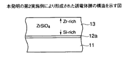
このようにして、新たな所定回数X1およびY1を使ってステップ1〜7を実行し、さらに前記所定回数を変化さながら前記ステップ1〜7を繰り返し実行することにより、図8に示すように、ZrとSiの比率が膜厚方向に連続的に変化する、組成がZrSiO4で表される誘電体膜を、前記Si基板11上に形成することができる。ただし、図8中、先に説明した部分は対応する参照符号で示してある。
【0036】
図8を参照するに、図示の例では、前記誘電体膜中のZrの組成が、前記Si基板11との界面近傍において小さく、前記界面から離れるにつれて徐々に減少するように制御されている。このように組成を制御されたZrSiO4膜では、前記Si基板11との界面近傍においてSi濃度が高いため、Si基板に対して優れた密着性が得られ、さらにZrSiO4膜の表面近傍ではZr濃度が高いため大きな誘電率が得られると共に、膜中を流れるリーク電流を抑制することが可能になる。また、前記ZrSiO4膜を、膜中においてZrとSiとが1分子層毎に互に配列するように形成することも可能である。
[第3実施例]
図9は、本発明の第3実施例による誘電体膜構造を示す。ただし図9中、先に説明した部分には対応する参照符号を付し、説明を省略する。
【0037】
図9を参照するに、本実施例では前記SiO2分子層12aが形成された後、SiCl4分子を前記SiO2分子層12aに吸着させ、さらにNH3ガスで前記吸着したSiCl4分子層を処理し、SiN分子層12dに変換する。かかるSiN分子層12dの形成の後、前記SiN分子層12dにTa(OC2H5)5分子を吸着させ、さらにこれを酸化させて前記Ta2O5分子層12cを形成した後、前記Ta2O5分子層12c上に前記CVD−Ta2O5膜13を形成する。
【0038】
図9の構造では、前記Ta2O5膜13とSi基板11との間にSiN分子層12dが介在しているため、例えば前記Ta2O5膜13上にBでドープしたポリシリコン膜を堆積したような場合でも、BのSi基板11中への拡散が前記SiN分子層12dにより阻止されるため、前記Ta2O5膜13をゲート絶縁膜に使った半導体装置において、しきい値電圧の変動を抑制することが可能になる。
[第4実施例]
図10は、本発明の第4実施例による半導体装置の構成を示す。
【0039】
図10を参照するに、p型Si基板21上には先に説明したいずれかの実施例に従って、Ta2O5よりなるゲート絶縁膜22が形成されており、前記ゲート絶縁膜22上にはポリシリコンゲート電極23が形成されている。
【0040】
さらに前記Si基板21中には、前記ゲート電極23に隣接してn-型の拡散領域21A,21Bが形成されており、前記ポリシリコンゲート電極23の側壁面は側壁絶縁膜23a,23bにより覆われている。さらに前記Si基板21中には、前記側壁絶縁膜23a,23bの外側に、n+型の拡散領域21C,21Dが形成されている。
【0041】
図10の半導体装置では、ゲート絶縁膜22としてTa2O5を使うため、0.1nm以下の厚さのSiO2膜に実質的に等価な実効膜厚が得られ、その結果ゲート長を短縮することにより、ゲートリーク電流を抑制しつつ、非常に高速な動作を実現することが可能になる。その際、先に説明した実施例に従って前記Ta2O5膜22を形成することにより、膜厚の変動を抑制でき、得られる半導体装置の特性を安定化させることができる。特に、前記Ta2O5膜22の直下に数分子層程度のSiO2分子層12aを介在させることにより、ゲート電極23からSi基板21への不純物元素の拡散が阻止され、半導体装置の特性が安定化する。さらに、前記ゲート絶縁膜22を、Ta2O5を含む様々な酸化物材料により、一分子層ずつ形成することにより、前記ゲート絶縁膜22内部の厚さ方向への組成分布を、自在に制御することが可能になる。その結果、Si基板との界面において密着性が高く、ゲート電極23との界面において比誘電率の大きい構造を容易に得ることが可能になる。その際、本発明では前記基板上への誘電体分子層の形成を、吸着された気相原料分子に対してプラズマ励起ラジカルを作用させるのではなく、吸着された気相原料分子を加水分解させることにより行うが、このように加水分解反応を使うことにより、従来の技術、特に先に説明した特開平11−87341号公報記載の技術と異なり、荷電粒子が誘電体膜中に取り込まれ、これがリーク電流路を形成する問題を回避することが可能になる。また、加水分解反応では、熱的に安定な反応しか生じないので、制御が容易である。
【0042】
【発明の効果】
本発明の特徴によれば、Si基板上に、薄い絶縁膜を隔ててTa2O5等の高誘電体膜、あるいは様々な組成の誘電体膜をCVD法により形成する際に、インキュベーション時間が実質的に減少し、その結果、形成される誘電体膜の均一性が向上する。さらに、形成される誘電体膜の膜厚方向への組成の制御を自在に行うことが可能で、また必要に応じて、1分子層程度の非常に薄い拡散障壁膜を、前記誘電体膜中に作りこむことが可能になる。本発明ではかかる誘電体膜の形成の際に、プラズマ励起されたラジカルを吸着させる工程が含まれないので、形成される誘電体膜は電荷の伴う準位等の欠陥を含まず、このため優れたリーク電流特性を示す。
【図面の簡単な説明】
【図1】(A)〜(C)は、本発明の第1実施例による誘電体膜の形成方法を示す図(その1)である。
【図2】(D)〜(F)は、本発明の第1実施例による誘電体膜の形成方法を示す図(その2)である。
【図3】(G)〜(H)は、本発明の第1実施例による誘電体膜の形成方法を示す図(その3)である。
【図4】本発明の効果を示す図である。
【図5】(A),(B)は、従来のCVD法によりSiON膜上に形成したTa2 O5 膜の表面構造を示す図である。
【図6】(A)は、本発明の方法によりSiON膜上に形成したTa2O5膜の表面構造を示す図、(B)は、Si基板の表面に直接に形成されたTa2O5膜の表面構造を示す図である。
【図7】本発明の第2実施例による誘電体膜の形成方法を示すフローチャートである。
【図8】本発明の第2実施例により形成された誘電体膜の構造を示す図である。
【図9】本発明の第3実施例により形成された誘電体膜の構造を示す図である。
【図10】本発明の第4実施例による半導体装置の構成を示す図である。
【符号の説明】
11,21 Si基板
11a 自然酸化膜
11b 保護膜
11c Si基板表面
12a SiO2分子層
12b Ta(OC2H5)5分子層
12c Ta2O5分子層
12d SiN分子層
13 CVD膜
22 ゲート絶縁膜
23 ゲート電極
23A,23B 側壁絶縁膜
21A,21B LDD拡散領域
21C,21D 拡散領域[0001]
BACKGROUND OF THE INVENTION
The present invention relates to a semiconductor device, and more particularly to a method for manufacturing an ultrafine high-speed semiconductor device having a high dielectric film.
[0002]
In today's ultrahigh-speed and high-speed semiconductor devices, gate lengths of 0.1 μm or less are becoming possible as the miniaturization process advances. In general, the operation speed of a semiconductor device increases with miniaturization. However, in such a semiconductor device that is extremely miniaturized, the thickness of the gate insulating film is reduced according to the scaling law as the gate length is shortened by miniaturization. It is necessary to let
[0003]
[Prior art]
However, when the gate length is 0.1 μm or less, the thickness of the gate insulating film needs to be set to 1 to 2 nm or less when SiO 2 is used, but in such a very thin gate insulating film, The problem that the tunnel current increases and, as a result, the gate leakage current increases cannot be avoided. For this reason, for example, as described in JP-A-11-87341, a very thin SiN film is adsorbed on the Si substrate surface, and a vapor phase raw material containing Si is adsorbed on the Si substrate surface. It is described that it is formed by the action of an atmosphere containing radicals. However, although the relative dielectric constant of the SiN film is larger than the relative dielectric constant of the SiO 2 film, it is only about 8. Therefore, when the SiN film is used, it satisfies the demand for miniaturization based on the scaling law. The gate insulating film cannot be formed to a substantial film thickness that can effectively block the tunnel current. In the method described in JP-A-11-87341, it is necessary to generate plasma in order to generate N radicals. However, if the substrate surface is processed in the vicinity of the plasma generation source, electrons caused by the plasma are generated. Since charged particles such as ions and ions are taken into the SiN film and form levels, the leakage current characteristics and CV characteristics of the resulting SiN film are degraded. On the other hand, if a plasma generation source is provided at a position away from the substrate in order to avoid this problem, the amount of necessary N radicals is greatly reduced, making it difficult to adsorb N.
[0004]
Conventionally In these circumstances, the dielectric constant is much larger than that of the SiO 2 film, when the actual thickness for this purpose in terms of SiO 2 film be greater thickness of less Ta 2 O 5 It has been proposed to apply such a high dielectric material to the gate insulating film. By using such a high-dielectric material such as Ta 2 O 5, a gate insulating film having a thickness of about 10 μm can be used even in a very short ultrahigh-speed semiconductor device having a gate length of 0.1 μm or less. The gate leakage current due to the tunnel effect can be suppressed.
[0005]
Conventionally, it is known that a Ta 2 O 5 film can be formed by a CVD method using Ta (OC 2 H 5 ) 5 and O 2 as vapor phase raw materials. Typically, the CVD process is performed at a temperature of about 480 ° C. or higher in a reduced pressure environment. The Ta 2 O 5 film thus formed is further heat-treated in an oxygen atmosphere. As a result, oxygen vacancies in the film are eliminated and the film itself is crystallized. The Ta 2 O 5 film thus crystallized exhibits a large relative dielectric constant.
[0006]
[Problems to be solved by the invention]
On the other hand, when a high dielectric film such as Ta 2 O 5 is grown on a Si substrate by the CVD method, the deposition of the high dielectric film does not start immediately even when the CVD process is started in relation to the nucleation process. It is known that film deposition begins only after a certain incubation time has elapsed.
[0007]
In the experiments that form the basis of the present invention, the inventors of the present invention have found that this incubation time varies depending on the nature of the substrate on which the high dielectric film is deposited. For example, if the substrate is a clean Si substrate from which the oxide film is removed, the incubation time is short, but if an SiO 2 film, SiN film, or SiON film is present on the surface of the Si substrate, the incubation time is short. Will increase. It has also been found that the incubation time depends on the thickness of the SiO 2 film, SiN film or SiON film. This is because the film thickness of the high dielectric film formed on the SiO 2 film, the SiN film or the SiON film is affected by the fluctuation of the film thickness of the base film, and as a result, the film thickness fluctuation of the base film is amplified. Means there is a tendency. In addition, the fact that the film thickness of the high dielectric film formed by the CVD method is affected by the underlying layer means that the film quality of the high dielectric film used for the gate insulating film or the like tends to be uneven. I mean.
[0008]
In order to suppress such film quality non-uniformity in the high dielectric film, it is desirable to reduce the incubation time as much as possible.
[0009]
Further, in a semiconductor device using such a high dielectric film as a gate insulating film, it is preferable to form the high dielectric film directly on the Si substrate in order to reduce the effective SiO 2 equivalent film thickness of the insulating film. However, from the viewpoint of improving carrier mobility in the gate channel, it is preferable to interpose a very thin oxide film between the high dielectric gate oxide film and the Si substrate. At that time, in order to maximize the effect of using the high dielectric film, a technique capable of changing the film quality, particularly the composition, of the high dielectric film in the film thickness direction is required. When the oxide film is thick, or when a region rich in Si is formed over a substantial thickness in the high dielectric film, the effect of the high dielectric film characterized by a high dielectric constant is It will decrease substantially.
[0010]
Therefore, a specific object of the present invention is to provide a novel and useful method for forming a dielectric film, which solves the above problems.
[0011]
A more specific object of the present invention is to form a dielectric film by a vapor deposition method, and incubate the dielectric film without causing a problem of damage caused by charged particles on the dielectric film. It is to minimize time and reduce surface roughness.
[0012]
Another object of the present invention is to provide a composition distribution in the film thickness direction of the dielectric film in the method for forming a dielectric film by a vapor deposition method without causing a problem of damage to the dielectric film due to charged particles. It is to provide a method capable of freely controlling the above.
[0013]
[Means for Solving the Problems]
The present invention solves the above problems .
In a method for forming a dielectric film on a Si substrate,
Forming an insulating layer on the Si substrate;
A step of substantially uniformly adsorbing a gas phase molecular compound of a metal element on the insulating layer at least once, and covering the insulating layer with the gas phase molecular compound;
Wherein said vapor phase molecular compound for covering the insulating layer is decomposed in an oxidizing atmosphere, viewed including the steps of forming a molecular layer of a dielectric material, a containing the metal element on the insulating layer,
After the step of decomposing the gas phase molecular compound, more formation how a dielectric film which comprises a step of forming by the CVD method a high dielectric film on the molecular layer of the dielectric, resolve .
[0014]
DETAILED DESCRIPTION OF THE INVENTION
[First embodiment]
1A to 1C show a method of forming a Ta 2 O 5 film according to a first embodiment of the present invention.
[0015]
Referring to FIG. 1A, the
[0016]
The
[0017]
2D, the internal pressure of the reaction vessel is set to 1.33-13.3 Pa (0.01-0.1 Torr) and the substrate temperature is set to 200-350 ° C. In succession to the step (C), SiCl 4 gas is introduced into the reaction vessel at a rate of 0.1 to 5 mg / min together with a He carrier gas having a flow rate of about 50 sccm, and SiCl 4 molecules are introduced into the
[0018]
Next, in the step of FIG. 2E, the substrate temperature is set to 350 ° C. or lower, preferably about 300 ° C. or lower, more preferably about 280 ° C., and the internal pressure is set to 0.01 to 0.1 Torr as before. The Ta (OC 2 H 5 ) O 5 gas and the O 2 gas are supplied together with the He carrier gas at a flow rate of about 5 mg / min and 100 sccm, respectively, for about 1 minute. The flow rate of the He carrier gas is set to about 100 sccm. As a result, as shown in FIG. 2 (F), the Ta (OC 2 H 5 ) O 5 molecules are adsorbed on the SiO 2 film 12a, and the Ta (OC 2 H 5 ) O 5 adsorbed
[0019]
Further, in the step of FIG. 3G, the substrate temperature is raised to about 350 ° C. in an oxidizing atmosphere such as O 2 to oxidize or hydrolyze the adsorbed Ta (OC 2 H 5 ) O 5 molecules, The adsorption
[0020]
Further, in the step of FIG. 3 (H), the substrate temperature is set to 510 ° C., the internal pressure of the reaction vessel is set to 13.3 to 1330 Pa (0.1 to 10 Torr), and Ta (OC 2 H 5 ) O 5 gas and O 2 gas are supplied together with a He carrier gas, and a Ta 2 O 5 film 13 is formed on the Ta 2 O 5
[0021]
Further, although not shown in the figure, the Ta 2 O 5 film 13 formed in this way is heat-treated in an O 2 atmosphere, so that oxygen vacancies in the
[0022]
FIG. 4 shows the relationship between the deposition time in the CVD process of FIG. 3H and the Ta 2 O 5 film 13 deposited as a result compared with the conventional Ta 2 O 5 film CVD process. Show. However, the deposition time is measured from the start of the CVD process. In FIG. 4, ♦ indicates the deposition of the Ta 2 O 5 film 13 according to the present embodiment, while ▲ indicates the deposition of the Ta 2 O 5 film in the conventional CVD process. However, in the conventional case indicated by ▲, a Ta 2 O 5 film is directly deposited on the SiO 2
[0023]
Referring to FIG. 4, the conventional CVD process requires about 140 seconds of incubation time from the start of the CVD process until the Ta 2 O 5 film is actually deposited. In the exemplary process, Ta 2 O 5 film deposition begins only 40 seconds after starting the CVD process. That is, with the configuration of this example, it is possible to substantially reduce the incubation time when the Ta 2 O 5 film is formed by the CVD method.
[0024]
5A and 5B show the result of observing the surface structure of the Ta 2 O 5 film formed on the SiON film covering the surface of the
[0025]
Referring to FIGS. 5A and 5B, the CVD-Ta 2 O 5 film formed in this way reflects a film thickness variation of the underlying SiON film and has a very large film thickness variation. It can be seen that In other words, in the conventional CVD-Ta 2 O 5 film, the film thickness variation of the base film is amplified, and the resulting film thickness of the Ta 2 O 5 film becomes non-uniform.
[0026]
On the other hand, FIG. 6 (A) shows the surface structure of the Ta 2 O 5 film formed by the steps of the present embodiment shown in FIGS. 1 (A) to 3 (G). However, in FIG. 6A, a SiON molecular layer is used instead of the SiO 2
[0027]
Referring to FIG. 6A, by adopting the process according to the present embodiment, the unevenness of the Ta 2 O 5 film surface formed by the CVD method is substantially reduced and formed directly on the Si substrate. It turns out that it will be in a state close to the case. This is because the vapor phase molecular compound Ta (OC 2 H 5 ) 5 of Ta is adsorbed on the underlying SiON film described above with reference to FIG. 4 and oxidized to form a Ta 2 O 5
[0028]
Note that the gas phase molecular compound used when forming the Ta 2 O 5
[0029]
Furthermore, the method of this example is not limited to the formation of the Ta 2 O 5 film. As shown in Tables 1 and 2 below, SiO 2 , ZrO 2 or HfO 2 , and further Al 2 O. It is also applicable to the formation of oxide films such as 3 . However, Table 1 summarizes the process conditions of the gas phase molecular compound adsorption process and oxidation process of FIGS. 2 (F) and 3 (G), and Table 2 summarizes the process conditions of the CVD process of FIG. 3 (H). Show.
[0030]
[Table 1]
[Table 2]
[0032]
Further, as can be seen from Table 1, when a ZrO 2 molecular layer is formed as the
[0033]
Furthermore, a CVD process of Ta 2 O 5 , ZrO 2 , HfO 2 , SiO 2, or Al 2 O 3 is performed by performing a CVD process on the oxide
[Second Embodiment]
FIG. 7 is a flowchart showing a method of forming a dielectric film according to the second embodiment of the present invention.
[0034]
Referring to FIG. 7, SiCl 4 molecules are adsorbed on the SiO 2
[0035]
In this way, steps 1 to 7 are executed using the new predetermined times X 1 and Y 1 , and further, the steps 1 to 7 are repeatedly executed while changing the predetermined times, as shown in FIG. A dielectric film whose composition is expressed by ZrSiO 4 in which the ratio of Zr and Si continuously changes in the film thickness direction can be formed on the
[0036]
Referring to FIG. 8, in the illustrated example, the composition of Zr in the dielectric film is controlled to be small in the vicinity of the interface with the
[Third embodiment]
FIG. 9 shows a dielectric film structure according to a third embodiment of the present invention. However, in FIG. 9, the parts described above are denoted by the corresponding reference numerals, and the description thereof is omitted.
[0037]
Referring to FIG. 9, in this embodiment, after the SiO 2
[0038]
In the structure of FIG. 9, since the SiN
[Fourth embodiment]
FIG. 10 shows a configuration of a semiconductor device according to the fourth embodiment of the present invention.
[0039]
Referring to FIG. 10, a
[0040]
Further, n −
[0041]
In the semiconductor device of FIG. 10, since Ta 2 O 5 is used as the
[0042]
【The invention's effect】
According to the characteristics of the present invention, when a high dielectric film such as Ta 2 O 5 or a dielectric film having various compositions is formed on a Si substrate with a thin insulating film therebetween by a CVD method, the incubation time is increased. This is substantially reduced, and as a result, the uniformity of the formed dielectric film is improved. Furthermore, it is possible to freely control the composition in the film thickness direction of the dielectric film to be formed, and if necessary, an extremely thin diffusion barrier film of about one molecular layer is formed in the dielectric film. It becomes possible to make it. In the present invention, the formation of such a dielectric film does not include a step of adsorbing plasma-excited radicals. Therefore, the formed dielectric film does not include defects such as a level accompanied by electric charge, and thus is excellent. Shows leakage current characteristics.
[Brief description of the drawings]
FIGS. 1A to 1C are views (No. 1) illustrating a method for forming a dielectric film according to a first embodiment of the present invention. FIGS.
FIGS. 2D to 2F are views (No. 2) showing a method of forming a dielectric film according to the first embodiment of the present invention. FIGS.
FIGS. 3G to 3H are views (No. 3) showing the method for forming a dielectric film according to the first embodiment of the present invention. FIGS.
FIG. 4 is a diagram showing the effect of the present invention.
5A and 5B are diagrams showing the surface structure of a Ta2 O5 film formed on a SiON film by a conventional CVD method.
6A is a view showing the surface structure of a Ta 2 O 5 film formed on a SiON film by the method of the present invention, and FIG. 6B is a view showing Ta 2 O formed directly on the surface of a Si substrate. It is a figure which shows the surface structure of 5 films | membranes.
FIG. 7 is a flowchart illustrating a method of forming a dielectric film according to a second embodiment of the present invention.
FIG. 8 is a diagram showing a structure of a dielectric film formed according to a second embodiment of the present invention.
FIG. 9 is a diagram showing a structure of a dielectric film formed according to a third embodiment of the present invention.
FIG. 10 is a diagram showing a configuration of a semiconductor device according to a fourth embodiment of the present invention.
[Explanation of symbols]
11, 21
Claims (13)
前記Si基板上に絶縁性層を形成する工程と、
前記絶縁性層上に少なくとも1回、金属元素の気相分子化合物を実質的に一様に吸着させ、前記絶縁性層上を前記気相分子化合物により覆う工程と、
前記絶縁層を覆う前記気相分子化合物を酸化雰囲気中で分解し、前記絶縁層上に前記金属元素を含む誘電体材料の分子層を形成する工程と、を含み、
前記気相分子化合物を分解させる工程の後、前記誘電体の分子層上に高誘電体膜をCVD法により形成する工程を含むことを特徴とする誘電体膜の形成方法。In a method for forming a dielectric film on a Si substrate,
Forming an insulating layer on the Si substrate;
A step of substantially uniformly adsorbing a gas phase molecular compound of a metal element on the insulating layer at least once, and covering the insulating layer with the gas phase molecular compound;
Wherein said vapor phase molecular compound for covering the insulating layer is decomposed in an oxidizing atmosphere, viewed including the steps of forming a molecular layer of a dielectric material, a containing the metal element on the insulating layer,
A method for forming a dielectric film, comprising: after the step of decomposing the gas phase molecular compound, forming a high dielectric film on the dielectric molecular layer by a CVD method.
Priority Applications (6)
| Application Number | Priority Date | Filing Date | Title |
|---|---|---|---|
| JP2000095818A JP4493796B2 (en) | 2000-03-30 | 2000-03-30 | Method for forming dielectric film |
| KR1020027012657A KR100752559B1 (en) | 2000-03-30 | 2001-03-22 | Method of forming a dielectric film |
| US10/239,648 US6866890B2 (en) | 2000-03-30 | 2001-03-22 | Method of forming a dielectric film |
| EP01915684A EP1269528B1 (en) | 2000-03-30 | 2001-03-22 | Method of forming a dielectric film |
| PCT/JP2001/002262 WO2001075956A1 (en) | 2000-03-30 | 2001-03-22 | Method of forming a dielectric film |
| TW090107295A TW486762B (en) | 2000-03-30 | 2001-03-28 | Method of forming a dielectric film |
Applications Claiming Priority (1)
| Application Number | Priority Date | Filing Date | Title |
|---|---|---|---|
| JP2000095818A JP4493796B2 (en) | 2000-03-30 | 2000-03-30 | Method for forming dielectric film |
Related Child Applications (1)
| Application Number | Title | Priority Date | Filing Date |
|---|---|---|---|
| JP2009280314A Division JP2010056582A (en) | 2009-12-10 | 2009-12-10 | Method of forming dielectric film |
Publications (3)
| Publication Number | Publication Date |
|---|---|
| JP2001284344A JP2001284344A (en) | 2001-10-12 |
| JP2001284344A5 JP2001284344A5 (en) | 2007-05-10 |
| JP4493796B2 true JP4493796B2 (en) | 2010-06-30 |
Family
ID=18610667
Family Applications (1)
| Application Number | Title | Priority Date | Filing Date |
|---|---|---|---|
| JP2000095818A Expired - Fee Related JP4493796B2 (en) | 2000-03-30 | 2000-03-30 | Method for forming dielectric film |
Country Status (6)
| Country | Link |
|---|---|
| US (1) | US6866890B2 (en) |
| EP (1) | EP1269528B1 (en) |
| JP (1) | JP4493796B2 (en) |
| KR (1) | KR100752559B1 (en) |
| TW (1) | TW486762B (en) |
| WO (1) | WO2001075956A1 (en) |
Families Citing this family (19)
| Publication number | Priority date | Publication date | Assignee | Title |
|---|---|---|---|---|
| JP4095326B2 (en) | 2002-03-29 | 2008-06-04 | 株式会社東芝 | Semiconductor device manufacturing method and semiconductor device |
| JP2004140292A (en) | 2002-10-21 | 2004-05-13 | Tokyo Electron Ltd | Forming method of dielectric film |
| JP2005093909A (en) * | 2003-09-19 | 2005-04-07 | Tokyo Electron Ltd | Substrate processing method and substrate processing apparatus |
| JP2005317583A (en) * | 2004-04-27 | 2005-11-10 | Renesas Technology Corp | Semiconductor device and its manufacturing method |
| JP4582542B2 (en) * | 2005-02-02 | 2010-11-17 | 株式会社神戸製鋼所 | Diamond field effect transistor and manufacturing method thereof |
| US7235502B2 (en) * | 2005-03-31 | 2007-06-26 | Freescale Semiconductor, Inc. | Transitional dielectric layer to improve reliability and performance of high dielectric constant transistors |
| FR2890982B1 (en) * | 2005-09-21 | 2008-05-02 | St Microelectronics Sa | METHOD FOR PRODUCING A DIELECTRIC LAYER ON A CARRIER MATERIAL AND AN INTEGRATED CIRCUIT COMPRISING A CAPACITOR INCORPORATING A DIELECTRIC LAYER |
| JP4722876B2 (en) * | 2007-04-16 | 2011-07-13 | 東京エレクトロン株式会社 | Method for forming metal oxide film |
| DE102007018013A1 (en) * | 2007-04-17 | 2008-10-23 | Qimonda Ag | Dielectric layer and method for producing a dielectric layer |
| KR101451716B1 (en) * | 2008-08-11 | 2014-10-16 | 도쿄엘렉트론가부시키가이샤 | Film forming method and film forming apparatus |
| JP5419420B2 (en) * | 2008-11-04 | 2014-02-19 | 東京エレクトロン株式会社 | Film forming method, film forming apparatus, and storage medium |
| US8667908B2 (en) | 2010-06-02 | 2014-03-11 | Steelcase Inc. | Frame type table assemblies |
| US9185974B2 (en) | 2010-06-02 | 2015-11-17 | Steelcase Inc. | Frame type workstation configurations |
| US9210999B2 (en) | 2010-06-02 | 2015-12-15 | Steelcase Inc. | Frame type table assemblies |
| US8534752B2 (en) | 2010-06-02 | 2013-09-17 | Steelcase Inc. | Reconfigurable table assemblies |
| LU92795B1 (en) * | 2015-08-10 | 2017-02-14 | Luxembourg Inst Science & Tech List | SIO2 thin film produced by atomic layer deposition at room temperature |
| US10039374B2 (en) | 2016-05-13 | 2018-08-07 | Steelcase Inc. | Multi-tiered workstation assembly |
| US10517392B2 (en) | 2016-05-13 | 2019-12-31 | Steelcase Inc. | Multi-tiered workstation assembly |
| US10217626B1 (en) * | 2017-12-15 | 2019-02-26 | Mattson Technology, Inc. | Surface treatment of substrates using passivation layers |
Citations (6)
| Publication number | Priority date | Publication date | Assignee | Title |
|---|---|---|---|---|
| JPH02196427A (en) * | 1989-01-25 | 1990-08-03 | Nec Corp | Vapor growth method of metal oxide film |
| JPH02283022A (en) * | 1989-01-25 | 1990-11-20 | Hitachi Ltd | Manufacture of semiconductor device |
| JPH05102189A (en) * | 1991-08-13 | 1993-04-23 | Fujitsu Ltd | Formation method of thin film, silicon thin film and formation method of silicon thin-film transistor |
| JPH07131007A (en) * | 1993-11-02 | 1995-05-19 | Tadahiro Omi | Semiconductor device |
| JPH0977593A (en) * | 1995-09-14 | 1997-03-25 | Nissan Motor Co Ltd | Chemical vapor phase growing method and chemical vapor phase growing device |
| JPH09232542A (en) * | 1996-02-28 | 1997-09-05 | Nec Corp | Semiconductor device and manufacture thereof |
Family Cites Families (17)
| Publication number | Priority date | Publication date | Assignee | Title |
|---|---|---|---|---|
| DE1923279A1 (en) | 1969-05-07 | 1970-12-23 | Licentia Gmbh | Transistor with an isolated control electrode |
| JPH05315608A (en) | 1992-05-13 | 1993-11-26 | Tadahiro Omi | Semiconductor device |
| JPH06310687A (en) | 1993-04-20 | 1994-11-04 | Kawasaki Steel Corp | Semiconductor device and its manufacture |
| US5521423A (en) | 1993-04-19 | 1996-05-28 | Kawasaki Steel Corporation | Dielectric structure for anti-fuse programming element |
| KR0183732B1 (en) * | 1995-09-01 | 1999-03-20 | 김광호 | Method of manufacturing semiconductor device capacitor |
| JP2871580B2 (en) * | 1996-03-29 | 1999-03-17 | 日本電気株式会社 | Method for manufacturing semiconductor device |
| KR100207485B1 (en) * | 1996-07-23 | 1999-07-15 | 윤종용 | Manufacturing method of capacitors for semiconductor devices |
| US5858843A (en) | 1996-09-27 | 1999-01-12 | Intel Corporation | Low temperature method of forming gate electrode and gate dielectric |
| TW468253B (en) * | 1997-01-13 | 2001-12-11 | Hitachi Ltd | Semiconductor memory device |
| JPH10303372A (en) * | 1997-01-31 | 1998-11-13 | Sanyo Electric Co Ltd | Semiconductor integrated circuit and producing method therefor |
| US6589644B1 (en) * | 1997-05-28 | 2003-07-08 | Nippon Steel Corporation | Low dielectric constant materials and their production and use |
| US6020243A (en) | 1997-07-24 | 2000-02-01 | Texas Instruments Incorporated | Zirconium and/or hafnium silicon-oxynitride gate dielectric |
| US6475927B1 (en) | 1998-02-02 | 2002-11-05 | Micron Technology, Inc. | Method of forming a semiconductor device |
| EP1026213B1 (en) * | 1998-09-01 | 2014-11-05 | JGC Catalysts and Chemicals Ltd. | Coating fluid for forming low-permittivity silica-based coating film and substrate with low-permittivity coating film |
| US6558747B2 (en) * | 1999-09-29 | 2003-05-06 | Kabushiki Kaisha Toshiba | Method of forming insulating film and process for producing semiconductor device |
| JP4043705B2 (en) * | 2000-09-27 | 2008-02-06 | 株式会社東芝 | Semiconductor device manufacturing method, wafer processing apparatus, and wafer storage box |
| US6699797B1 (en) * | 2002-12-17 | 2004-03-02 | Intel Corporation | Method of fabrication of low dielectric constant porous metal silicate films |
-
2000
- 2000-03-30 JP JP2000095818A patent/JP4493796B2/en not_active Expired - Fee Related
-
2001
- 2001-03-22 WO PCT/JP2001/002262 patent/WO2001075956A1/en active Application Filing
- 2001-03-22 US US10/239,648 patent/US6866890B2/en not_active Expired - Fee Related
- 2001-03-22 KR KR1020027012657A patent/KR100752559B1/en not_active IP Right Cessation
- 2001-03-22 EP EP01915684A patent/EP1269528B1/en not_active Expired - Lifetime
- 2001-03-28 TW TW090107295A patent/TW486762B/en not_active IP Right Cessation
Patent Citations (6)
| Publication number | Priority date | Publication date | Assignee | Title |
|---|---|---|---|---|
| JPH02196427A (en) * | 1989-01-25 | 1990-08-03 | Nec Corp | Vapor growth method of metal oxide film |
| JPH02283022A (en) * | 1989-01-25 | 1990-11-20 | Hitachi Ltd | Manufacture of semiconductor device |
| JPH05102189A (en) * | 1991-08-13 | 1993-04-23 | Fujitsu Ltd | Formation method of thin film, silicon thin film and formation method of silicon thin-film transistor |
| JPH07131007A (en) * | 1993-11-02 | 1995-05-19 | Tadahiro Omi | Semiconductor device |
| JPH0977593A (en) * | 1995-09-14 | 1997-03-25 | Nissan Motor Co Ltd | Chemical vapor phase growing method and chemical vapor phase growing device |
| JPH09232542A (en) * | 1996-02-28 | 1997-09-05 | Nec Corp | Semiconductor device and manufacture thereof |
Also Published As
| Publication number | Publication date |
|---|---|
| JP2001284344A (en) | 2001-10-12 |
| EP1269528B1 (en) | 2012-06-20 |
| US20040005408A1 (en) | 2004-01-08 |
| WO2001075956A1 (en) | 2001-10-11 |
| US6866890B2 (en) | 2005-03-15 |
| KR100752559B1 (en) | 2007-08-29 |
| EP1269528A1 (en) | 2003-01-02 |
| TW486762B (en) | 2002-05-11 |
| KR20020095194A (en) | 2002-12-20 |
Similar Documents
| Publication | Publication Date | Title |
|---|---|---|
| JP4493796B2 (en) | Method for forming dielectric film | |
| KR100640638B1 (en) | Method for forming high dielectric film by atomic layer deposition and method of fabricating semiconductor device having high dielectric film | |
| US7544996B2 (en) | Methods of fabricating a semiconductor device having a metal gate pattern | |
| US6544875B1 (en) | Chemical vapor deposition of silicate high dielectric constant materials | |
| US7473994B2 (en) | Method of producing insulator thin film, insulator thin film, method of manufacturing semiconductor device, and semiconductor device | |
| US7727911B2 (en) | Method for forming a gate insulating film | |
| US20060199384A1 (en) | Method of forming thin film, and method of manufacturing semiconductor device | |
| JP2004523885A (en) | Surface adjustment method before deposition | |
| JP2003218108A (en) | CVD DEPOSITION OF M-SiO GATE DIELECTRIC | |
| JP4574951B2 (en) | Semiconductor device and manufacturing method thereof | |
| JP2004165625A (en) | Plasma method for manufacturing oxide thin film | |
| JP2002359371A (en) | Semiconductor device and its manufacturing method | |
| US7786021B2 (en) | High-density plasma multilayer gate oxide | |
| JP2007235093A (en) | Method for manufacturing semiconductor device | |
| US7759736B2 (en) | Oxide interface with improved oxygen bonding | |
| US20070170502A1 (en) | Semiconductor device and method for manufacturing the same | |
| JP2010056582A (en) | Method of forming dielectric film | |
| US20040214365A1 (en) | Deposition oxide with improved oxygen bonding | |
| JP5141321B2 (en) | Manufacturing method of semiconductor device | |
| JP2004289082A (en) | Method of forming high-dielectric-constant gate insulating film | |
| KR100650758B1 (en) | Method for forming gate of semiconductor device |
Legal Events
| Date | Code | Title | Description |
|---|---|---|---|
| A521 | Request for written amendment filed |
Free format text: JAPANESE INTERMEDIATE CODE: A523 Effective date: 20070314 |
|
| A621 | Written request for application examination |
Free format text: JAPANESE INTERMEDIATE CODE: A621 Effective date: 20070314 |
|
| A131 | Notification of reasons for refusal |
Free format text: JAPANESE INTERMEDIATE CODE: A131 Effective date: 20091013 |
|
| A521 | Request for written amendment filed |
Free format text: JAPANESE INTERMEDIATE CODE: A523 Effective date: 20091210 |
|
| TRDD | Decision of grant or rejection written | ||
| A01 | Written decision to grant a patent or to grant a registration (utility model) |
Free format text: JAPANESE INTERMEDIATE CODE: A01 Effective date: 20100406 |
|
| A01 | Written decision to grant a patent or to grant a registration (utility model) |
Free format text: JAPANESE INTERMEDIATE CODE: A01 |
|
| A61 | First payment of annual fees (during grant procedure) |
Free format text: JAPANESE INTERMEDIATE CODE: A61 Effective date: 20100407 |
|
| R150 | Certificate of patent or registration of utility model |
Free format text: JAPANESE INTERMEDIATE CODE: R150 |
|
| FPAY | Renewal fee payment (event date is renewal date of database) |
Free format text: PAYMENT UNTIL: 20130416 Year of fee payment: 3 |
|
| FPAY | Renewal fee payment (event date is renewal date of database) |
Free format text: PAYMENT UNTIL: 20160416 Year of fee payment: 6 |
|
| LAPS | Cancellation because of no payment of annual fees |