JP4493646B2 - Buffer structure for modifying a silicon substrate for subsequent target material deposition and method of forming the buffer structure - Google Patents
Buffer structure for modifying a silicon substrate for subsequent target material deposition and method of forming the buffer structure Download PDFInfo
- Publication number
- JP4493646B2 JP4493646B2 JP2006502270A JP2006502270A JP4493646B2 JP 4493646 B2 JP4493646 B2 JP 4493646B2 JP 2006502270 A JP2006502270 A JP 2006502270A JP 2006502270 A JP2006502270 A JP 2006502270A JP 4493646 B2 JP4493646 B2 JP 4493646B2
- Authority
- JP
- Japan
- Prior art keywords
- buffer
- layer
- target material
- buffer structure
- alloy
- Prior art date
- Legal status (The legal status is an assumption and is not a legal conclusion. Google has not performed a legal analysis and makes no representation as to the accuracy of the status listed.)
- Expired - Fee Related
Links
Images


Classifications
-
- C—CHEMISTRY; METALLURGY
- C30—CRYSTAL GROWTH
- C30B—SINGLE-CRYSTAL GROWTH; UNIDIRECTIONAL SOLIDIFICATION OF EUTECTIC MATERIAL OR UNIDIRECTIONAL DEMIXING OF EUTECTOID MATERIAL; REFINING BY ZONE-MELTING OF MATERIAL; PRODUCTION OF A HOMOGENEOUS POLYCRYSTALLINE MATERIAL WITH DEFINED STRUCTURE; SINGLE CRYSTALS OR HOMOGENEOUS POLYCRYSTALLINE MATERIAL WITH DEFINED STRUCTURE; AFTER-TREATMENT OF SINGLE CRYSTALS OR A HOMOGENEOUS POLYCRYSTALLINE MATERIAL WITH DEFINED STRUCTURE; APPARATUS THEREFOR
- C30B23/00—Single-crystal growth by condensing evaporated or sublimed materials
- C30B23/02—Epitaxial-layer growth
-
- C—CHEMISTRY; METALLURGY
- C30—CRYSTAL GROWTH
- C30B—SINGLE-CRYSTAL GROWTH; UNIDIRECTIONAL SOLIDIFICATION OF EUTECTIC MATERIAL OR UNIDIRECTIONAL DEMIXING OF EUTECTOID MATERIAL; REFINING BY ZONE-MELTING OF MATERIAL; PRODUCTION OF A HOMOGENEOUS POLYCRYSTALLINE MATERIAL WITH DEFINED STRUCTURE; SINGLE CRYSTALS OR HOMOGENEOUS POLYCRYSTALLINE MATERIAL WITH DEFINED STRUCTURE; AFTER-TREATMENT OF SINGLE CRYSTALS OR A HOMOGENEOUS POLYCRYSTALLINE MATERIAL WITH DEFINED STRUCTURE; APPARATUS THEREFOR
- C30B29/00—Single crystals or homogeneous polycrystalline material with defined structure characterised by the material or by their shape
- C30B29/10—Inorganic compounds or compositions
- C30B29/40—AIIIBV compounds wherein A is B, Al, Ga, In or Tl and B is N, P, As, Sb or Bi
- C30B29/403—AIII-nitrides
- C30B29/406—Gallium nitride
-
- H—ELECTRICITY
- H01—ELECTRIC ELEMENTS
- H01L—SEMICONDUCTOR DEVICES NOT COVERED BY CLASS H10
- H01L21/00—Processes or apparatus adapted for the manufacture or treatment of semiconductor or solid state devices or of parts thereof
- H01L21/02—Manufacture or treatment of semiconductor devices or of parts thereof
- H01L21/02104—Forming layers
- H01L21/02365—Forming inorganic semiconducting materials on a substrate
- H01L21/02367—Substrates
- H01L21/0237—Materials
- H01L21/02373—Group 14 semiconducting materials
- H01L21/02381—Silicon, silicon germanium, germanium
-
- H—ELECTRICITY
- H01—ELECTRIC ELEMENTS
- H01L—SEMICONDUCTOR DEVICES NOT COVERED BY CLASS H10
- H01L21/00—Processes or apparatus adapted for the manufacture or treatment of semiconductor or solid state devices or of parts thereof
- H01L21/02—Manufacture or treatment of semiconductor devices or of parts thereof
- H01L21/02104—Forming layers
- H01L21/02365—Forming inorganic semiconducting materials on a substrate
- H01L21/02436—Intermediate layers between substrates and deposited layers
- H01L21/02439—Materials
-
- H—ELECTRICITY
- H01—ELECTRIC ELEMENTS
- H01L—SEMICONDUCTOR DEVICES NOT COVERED BY CLASS H10
- H01L21/00—Processes or apparatus adapted for the manufacture or treatment of semiconductor or solid state devices or of parts thereof
- H01L21/02—Manufacture or treatment of semiconductor devices or of parts thereof
- H01L21/02104—Forming layers
- H01L21/02365—Forming inorganic semiconducting materials on a substrate
- H01L21/02436—Intermediate layers between substrates and deposited layers
- H01L21/02494—Structure
- H01L21/02496—Layer structure
- H01L21/02505—Layer structure consisting of more than two layers
-
- H—ELECTRICITY
- H01—ELECTRIC ELEMENTS
- H01L—SEMICONDUCTOR DEVICES NOT COVERED BY CLASS H10
- H01L21/00—Processes or apparatus adapted for the manufacture or treatment of semiconductor or solid state devices or of parts thereof
- H01L21/02—Manufacture or treatment of semiconductor devices or of parts thereof
- H01L21/02104—Forming layers
- H01L21/02365—Forming inorganic semiconducting materials on a substrate
- H01L21/02436—Intermediate layers between substrates and deposited layers
- H01L21/02494—Structure
- H01L21/02496—Layer structure
- H01L21/0251—Graded layers
-
- H—ELECTRICITY
- H01—ELECTRIC ELEMENTS
- H01L—SEMICONDUCTOR DEVICES NOT COVERED BY CLASS H10
- H01L21/00—Processes or apparatus adapted for the manufacture or treatment of semiconductor or solid state devices or of parts thereof
- H01L21/02—Manufacture or treatment of semiconductor devices or of parts thereof
- H01L21/02104—Forming layers
- H01L21/02365—Forming inorganic semiconducting materials on a substrate
- H01L21/02518—Deposited layers
- H01L21/02521—Materials
- H01L21/02538—Group 13/15 materials
- H01L21/0254—Nitrides
Abstract
Description
本発明は、後続のターゲット材堆積のためのシリコン基板を改質するバッファ構造、前記バッファ構造を組み入れた前駆体デバイス構造およびデバイス、ならびに前記構造およびデバイスを形成する方法に関する。詳細には、例えば、Si上のIII−V族半導体またはペロブスカイト酸化物などのターゲット材の成長に適し、特に窒化ガリウム材に適用されるバッファ構造に関する。 The present invention relates to a buffer structure for modifying a silicon substrate for subsequent target material deposition, a precursor device structure and device incorporating the buffer structure, and a method of forming the structure and device. Specifically, the present invention relates to a buffer structure suitable for growth of a target material such as a III-V semiconductor or a perovskite oxide on Si, and particularly applied to a gallium nitride material.
窒化ガリウム材は、幾多の超小型電子技術の用途において役立つ数々の魅力的な特性を有する半導体化合物である。一般に、窒化ガリウムは、エピタキシャル成長のメカニズムに影響を及ぼす適切な基板上に単結晶(エピタキシャル)層として成長させる必要がある。単結晶層は、バルク基板上に利益の上がる数量で成長させることが望ましいが、ヘテロエピタキシャル成長に適した基板を識別することは難しい。 Gallium nitride materials are semiconductor compounds with a number of attractive properties that are useful in many microelectronic applications. In general, gallium nitride must be grown as a single crystal (epitaxial) layer on a suitable substrate that affects the mechanism of epitaxial growth. Although it is desirable to grow single crystal layers in a profitable quantity on a bulk substrate, it is difficult to identify a substrate suitable for heteroepitaxial growth.
サファイア(Al2O3)、シリコンカーバイドおよびシリコンはみな、窒化ガリウムを堆積させるための基板として使用されているが、基板とターゲット材の特性がそれぞれ相異することによって、結果として得られる層の性質が制約されることがある。GaNは、上記の基板とは異なる熱膨張率を有するため、GaN層は処理後冷却されると、より厚い基板層による圧迫を受け、割れを生じやすい。窒化ガリウム層内に割れが生じると、その最終用途が厳しく制約される。 Sapphire (Al 2 O 3 ), silicon carbide and silicon are all used as substrates for depositing gallium nitride, but due to the different properties of the substrate and the target material, the resulting layers Properties may be constrained. Since GaN has a coefficient of thermal expansion different from that of the above substrate, when the GaN layer is cooled after processing, it is subject to compression by a thicker substrate layer and is likely to crack. If cracking occurs in the gallium nitride layer, its end use is severely restricted.
別の問題は、質の高いエピタキシャル成長を行うには、基板およびターゲット材の結晶格子定数は、同一であるか相当に近いものでなければならないということである。基板の表面構造および向きは、結果として得られるターゲット材層に強く影響を及ぼし、格子定数がうまく合致していない場合は、多数の転位が形成されターゲット材構造の微細な調整が利かなくなる。このような欠陥の形成は、結果として得られる単結晶の電子特性および/または光学特性に好ましからざる影響を及ぼすため、やはり最終用途が制約される。 Another problem is that for high quality epitaxial growth, the crystal lattice constants of the substrate and the target material must be the same or fairly close. The surface structure and orientation of the substrate strongly affects the resulting target material layer, and if the lattice constants do not match well, a large number of dislocations are formed and fine adjustment of the target material structure is lost. The formation of such defects also undesirably affects the electronic and / or optical properties of the resulting single crystal, thus limiting the end use.
遷移層およびバッファ層を使用する技法を含め、割れ形成および欠陥形成を防止するための従来技術の技法が開発されてきた。ヘテロエピタキシャル系内を突き進む転位を低減する1つの方策は、非結晶質または多結晶質のバッファ層を使用することである。例えば、モトローラ社のTFOS(Three Fives on Silicon)プロセスにおいては、基板上にコヒーレントな単結晶酸化膜を堆積させる。この酸化物が「臨界厚さ」に到達(この時点の厚さで多数の欠陥が現れる)する前に、基板から膜への界面が非結晶質層に変換される。この非結晶質層は、特定の材料に対して不整合歪みを吸収し、その結果転位密度が低くなる。歪み開放が起こる前に酸化物層がコヒーレントとなる必要があるため、層に対するこの手法によって不整合率が±5〜7%の範囲(この不整合率において、臨界厚さは1枚の原子単層を下回る)にとどまる。 Prior art techniques have been developed to prevent crack formation and defect formation, including techniques using transition layers and buffer layers. One strategy to reduce dislocations penetrating through the heteroepitaxial system is to use an amorphous or polycrystalline buffer layer. For example, in a Motorola TFOS (Three Fives on Silicon) process, a coherent single crystal oxide film is deposited on a substrate. Before the oxide reaches the “critical thickness” (a number of defects appear at this thickness), the substrate-to-film interface is converted to an amorphous layer. This amorphous layer absorbs mismatch strain for a specific material, resulting in a low dislocation density. Because the oxide layer needs to be coherent before strain relief occurs, this approach to the layer allows the misfit rate to be in the range of ± 5-7% (at this misfit rate, the critical thickness is one atomic unit). Stay below the stratum).
傾斜組成またはステップ組成の遷移層またはバッファ層を使用して質の高いヘテロエピタキシャル構造を実現できることが立証されている。傾斜層またはステップ層の役割は、歪みを徐々に導入し、それによって転位が移動する機会を提供することである。こうして、各不整合転位の長さを延ばし、転位が進む区域の消滅を促進することで、層表面に侵入する転位の数を低減させる。シリコン上に窒化ガリウム材を直接エピタキシャル成長させるための遷移層を使用する従来技術の技法は、組成傾斜GaNのAl合金およびIn合金を含む層を使用しているが大した成果があがっていない。 It has been demonstrated that high quality heteroepitaxial structures can be realized using graded or stepped transition or buffer layers. The role of the graded layer or step layer is to gradually introduce strain, thereby providing an opportunity for dislocations to move. Thus, the number of dislocations penetrating the layer surface is reduced by extending the length of each misfit dislocation and promoting the disappearance of the area where the dislocation advances. Prior art techniques that use transition layers for epitaxial growth of gallium nitride materials directly on silicon use layers containing Al and In alloys of compositionally graded GaN, but have not been very successful.
GaNおよび他のIII−V族半導体への技術的関心が高いため、17%の格子不整合があるにもかかわらず、Si基板上にGaNを成長させる数々の代替技術が開発されている。こうした技術には、パターニングされた基板上にGaNを成長させるペンドエピタキシ法(pendoepitaxy)およびELOG法(Epitaxial Lateral Overgrowth)、ならびにGaNを成長させる前にエチレン内でアニーリングすることによってSi基板をまずSiCに変換させる、いわゆるナイトロネックス(Nitronex)プロセスがある。ただし、こうしたプロセスの全てがSi層上にGaNの成長を成功裏に行っているが、欠陥密度は依然として必要以上にかなり高く、基板の予備処理によって生産コストが極めて高くなっている。 Due to the high technical interest in GaN and other III-V semiconductors, a number of alternative technologies for growing GaN on Si substrates have been developed despite the 17% lattice mismatch. These techniques include pend epitaxy and ELOG (Epitaxial Lateral Overgrowth) methods for growing GaN on a patterned substrate, and annealing in ethylene before growing GaN to first convert the Si substrate to SiC. There is a so-called Nitronex process to convert. However, all of these processes have successfully grown GaN on the Si layer, but the defect density is still much higher than necessary, and the substrate pre-treatment results in very high production costs.
本発明の第1の態様では、後続のターゲット材堆積のためのシリコン基板を改質するバッファ構造が提供される。バッファ構造は、IIIB族窒化物合金を含む組成傾斜(compositionally graded)バッファ層を含み、前記合金は2つ以上のIIIB族元素を含み、その相対量は、前記傾斜を達成するための深さによって変わる。 In a first aspect of the invention, a buffer structure is provided that modifies a silicon substrate for subsequent target material deposition. The buffer structure includes a compositionally graded buffer layer that includes a Group IIIB nitride alloy, the alloy including two or more Group IIIB elements, the relative amount of which depends on the depth to achieve the gradient. change.
IIIB族という用語は本明細書では、希土類元素Sc、Y、LaおよびAcを指すために使用する。これらの元素はいくつかの代替実施の下では、IIIA族元素としても知られている。 The term group IIIB is used herein to refer to the rare earth elements Sc, Y, La and Ac. These elements are also known as Group IIIA elements under some alternative implementations.
III−V族半導体という用語は、一般にN、P、As、SbまたはBiを有するB、Al、Ga、InまたはTlの化合物を指すのに使用される。 The term III-V semiconductor is generally used to refer to a compound of B, Al, Ga, In or Tl having N, P, As, Sb or Bi.
Si上にGaN合金および他のIII−V族半導体をエピタキシャルに堆積させることは、シリコンと、これらの材料との間に、熱膨張率の差があるばかりでなく、格子不整合が上記のように高い度合いであるため、かなりの難題である。本発明者は、それらが、IIIB族窒化物の物理特性および結晶構造によって、シリコン上に傾斜バッファ構造を提供するのに特に適したものとなり、それによって質の高いターゲット材層を堆積させることができるということを見出した。さらに、IIIB族窒化物においては、その各々の立方構造内の格子定数に十分な多様性があるため、エピタキシャル成長向けの「普遍的な」シリコンベース基板、つまり広範囲のターゲット材に適したように構成することができる基板の生成が容易になる。したがって、本発明は、質の高いGaNの成長に適したバッファ構造、ならびに、他のIII−V族半導体および技術的に重要なペロブスカイト酸化物などの材料を含め、広範囲にわたる他のターゲット材に適合可能な基板構造を提供するものである。 Epitaxially depositing GaN alloys and other III-V semiconductors on Si not only has a difference in thermal expansion between silicon and these materials, but also has a lattice mismatch as described above. This is a very difficult task. The inventors have made them particularly suitable for providing a graded buffer structure on silicon due to the physical properties and crystal structure of IIIB nitrides, thereby depositing a high quality target material layer. I found that I can do it. In addition, group IIIB nitrides are sufficiently diversified in their lattice constants within each cubic structure, so that they are suitable for “universal” silicon-based substrates for epitaxial growth, ie, a wide range of target materials. The generation of a substrate that can be facilitated. Thus, the present invention is compatible with a wide range of other target materials, including buffer structures suitable for high quality GaN growth, and other materials such as III-V semiconductors and technically important perovskite oxides. A possible substrate structure is provided.
本発明のさらなる態様では、シリコン基板上に上記のバッファ構造が設けられた結晶構造、ならびに上記のバッファ構造およびその上に設けられたターゲット材層を含む結晶構造も提供される。このような結晶構造を含む半導体デバイスも提供される。 In a further aspect of the present invention, there is also provided a crystal structure including the buffer structure described above on a silicon substrate, and a crystal structure including the buffer structure and a target material layer provided thereon. A semiconductor device including such a crystal structure is also provided.
さらなる態様では、後続のターゲット材堆積のためのシリコン基板を改質するバッファ構造を形成する方法が提供される。この方法は、IIIB族窒化物合金を含む、組成傾斜バッファ層をシリコン基板上に成長させる段階を含む。前記合金は、2つ以上のIIIB族元素を含み、その相対量は前記傾斜を達成するための深さによって変わる。 In a further aspect, a method is provided for forming a buffer structure that modifies a silicon substrate for subsequent target material deposition. The method includes growing a compositionally graded buffer layer comprising a IIIB nitride alloy on a silicon substrate. The alloy includes two or more Group IIIB elements, the relative amount of which varies depending on the depth to achieve the gradient.
好ましい態様では、後続のターゲット材堆積のためのシリコン基板を改質するバッファ構造が提供される。このバッファ構造は、窒化ランタン合金を含む組成傾斜バッファ層を含む。前記合金は、前記傾斜を達成するための、IIIB族からの1つまたは複数のさらなる元素をさらに含む。 In a preferred embodiment, a buffer structure is provided that modifies the silicon substrate for subsequent target material deposition. This buffer structure includes a composition gradient buffer layer containing a lanthanum nitride alloy. The alloy further includes one or more additional elements from group IIIB to achieve the gradient.
添付の図面を参照して本発明をさらに詳細に説明する。 The present invention will be described in more detail with reference to the accompanying drawings.
本発明者は、2つ以上のIIIB族元素(La、Y、ScまたはAc)を含む、組成傾斜合金層を含むバッファ構造を使用してシリコン基板を改質して、一連のターゲット材(例えばGaN)をその上に堆積させることができる適合性の高いバッファ構造を生成して、電子工学的および光学的用途の半導体デバイスを生成することができることを見出した。 The inventors have modified a silicon substrate using a buffer structure that includes a compositionally graded alloy layer that includes two or more Group IIIB elements (La, Y, Sc, or Ac) to provide a series of target materials (eg, It has been found that highly compatible buffer structures on which GaN) can be deposited can be produced to produce semiconductor devices for electronic and optical applications.
LaN、ScNおよびYNは全て、半金属または微小ギャップ半導体(例えば、ScNは約2.2eVのバンドギャップを有する)である。したがって、本発明によるバッファ構造は、例えば、デバイス底部に電気的コンタクトを必要とするLEDへの用途において導電性を選択することができ、あるいは例えば、マイクロ波FETへの用途においては高抵抗性とすることができる。 LaN, ScN and YN are all metalloid or microgap semiconductors (eg, ScN has a band gap of about 2.2 eV). Thus, the buffer structure according to the present invention can be selected for conductivity in, for example, LED applications that require electrical contact at the bottom of the device, or can be highly resistive in, for example, microwave FET applications. can do.
本明細書で使用するように、「シリコン基板」という用語は、例えば、バルクシリコンウェハ、シリコンオンインシュレータ基板、シリコンオンサファイア基板、SIMOX基板および別の多結晶材に結合されたシリコンウェハを有する基板を含め、単結晶シリコン層を含むどんな基板をも意味する。 As used herein, the term “silicon substrate” refers to, for example, a substrate having a silicon wafer bonded to a bulk silicon wafer, a silicon-on-insulator substrate, a silicon-on-sapphire substrate, a SIMOX substrate, and another polycrystalline material. Any substrate including a single crystal silicon layer is meant.
構造または層が基板または他の層の上にあると記載されている場合、その構造または層は、その基板または他の層の全体または一部分の上に直接配設されているか、中間層も存在する場合は間接的に配設されていることがある。 Where a structure or layer is described as being on a substrate or other layer, the structure or layer is disposed directly on all or a portion of the substrate or other layer, or an intermediate layer is also present In some cases, it may be indirectly arranged.
「組成傾斜」バッファ層内では、IIIB族元素それぞれの相対量は、バッファ層の少なくとも一部の厚さ全体を通して、バッファ層内で深さとともに変化する。相対量は、純粋な個々のIIIB族窒化物(例えば、LaNまたはScNの窒化物)それぞれの格子定数に関して、シリコン基板からの距離とともに格子定数が徐々に減少するように変化することができる。その層内には違う深さのところに、最低限でも2つの異なる組成が存在する。しかし通常は、単結晶または単一格子内のLa、ScまたはY原子それぞれの相対濃度内で緩やかに変化する。 Within the “composition gradient” buffer layer, the relative amount of each of the Group IIIB elements varies with depth within the buffer layer throughout the thickness of at least a portion of the buffer layer. The relative amount can vary with respect to the lattice constant of each pure individual group IIIB nitride (eg, LaN or ScN nitride) such that the lattice constant gradually decreases with distance from the silicon substrate. There are at least two different compositions at different depths in the layer. However, it usually changes slowly within the relative concentration of each of the La, Sc or Y atoms in the single crystal or single lattice.
不整合歪みを吸収するために、結晶構造がターゲットつまりGaN(ウルツァイト型)の結晶構造と適合性のあるInNまたはAlNなどの合金のバッファ層を使用する傾向にある従来技術のバッファシステムに対し、本発明は別の周期律の族つまりIIIB族からの元素を含む組成傾斜バッファ層の成長に基づいている。その結果得られる窒化物合金の格子は、以下にさらに説明するように、傾斜に応じた広範囲の格子定数変動、ならびにSiとやはりGaNに近い格子整合を達成することができる別の結晶構造(立方晶のNaCl)を有する。 For prior art buffer systems, which tend to use buffer layers of alloys such as InN or AlN whose crystal structure is compatible with the crystal structure of the target, i.e. GaN (Wurzite type), to absorb mismatch strains, The present invention is based on the growth of a compositionally graded buffer layer containing elements from another periodic group, ie group IIIB. The resulting nitride alloy lattice has another crystal structure (cubic) that can achieve a wide range of lattice constant variations as a function of tilt, as well as lattice matching close to that of Si and GaN, as further described below. Crystallized NaCl).
さらに、IIIB族元素は、シリコンよりもはるかに陽電性が低いことから、SiNに優先して窒化物を形成する。したがって、初期の結晶成長段階中は、露出した基板上での窒化ケイ素形成(この窒化物は非結晶質であり、基板とヘテロエピタキシャル層とのエピタキシャルな関係を妨害する)を防止する手順をとることが(従来技術のプロセスにおけるよりも)容易であり、製造プロセスの簡略化、低コストにつながる。 Furthermore, group IIIB elements form a nitride in preference to SiN because they are much less positive than silicon. Thus, during the initial crystal growth stage, steps are taken to prevent silicon nitride formation on the exposed substrate (this nitride is amorphous and interferes with the epitaxial relationship between the substrate and the heteroepitaxial layer). Is easier (than in prior art processes), leading to simplified manufacturing processes and lower costs.
合金は、ランタン、スカンジウムおよびイットリウムから選択された、少なくとも2つのIIIB族元素を含むことができる。LaN、YNおよびScNはみな立方晶(NaCl)構造を有し、格子定数はLaNが0.530nm、YNが0.489nmおよびScNが0.445nmである。シリコンは、相応する格子定数0.5431nmを有する。したがって、Si表面上での成長は、バッファ層用の出発組成物、例えば、純粋なLaNまたは純粋なYN、あるいは、より大きな窒化物パラメータを有し、元素濃度が約75%超、好ましくは90%以上の高濃度のLaYNまたはLaScNまたはYScNまたはLaYScNから始めることができる。その後、他の元素の量を、より大きなパラメータの元素量が25%以下、好ましくは10%以下に落ちるまで増加することができる。とりわけLaNは、特に格子整合がよいため、極めて低い転位密度を達成することが可能であり、したがって、これまで可能であったよりも質の高いエピタキシャル層をSi上に設けることができる。GaNがターゲット材の場合、108cm−2未満の転位密度ならびに1nm未満のRMS〔二乗平均平方根〕表面粗さを達成することができる。 The alloy can include at least two Group IIIB elements selected from lanthanum, scandium and yttrium. LaN, YN, and ScN all have a cubic (NaCl) structure, and the lattice constants are 0.530 nm for LaN, 0.489 nm for YN, and 0.445 nm for ScN. Silicon has a corresponding lattice constant of 0.5431 nm. Thus, growth on the Si surface has a starting composition for the buffer layer, such as pure LaN or pure YN, or higher nitride parameters, with elemental concentrations greater than about 75%, preferably 90%. It is possible to start with a high concentration of LaYN or LaScN or YScN or LaYScN. Thereafter, the amount of other elements can be increased until the larger parameter element amount falls below 25%, preferably below 10%. In particular, since LaN has particularly good lattice matching, it is possible to achieve a very low dislocation density, and therefore a higher quality epitaxial layer can be provided on Si than has been possible so far. When GaN is the target material, a dislocation density of less than 10 8 cm −2 and an RMS [root mean square] surface roughness of less than 1 nm can be achieved.
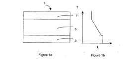
図1aは、単結晶シリコン基板上にLa(1−x)ScxN(0<x<1)のエピ層が堆積され、基板からの距離が遠ざかるにつれてx値が増加してIII−V族化合物のエピタキシャル成長に適したコンプライアント基板を提供する、好ましい実施形態を示している。結晶構造1は、シリコン基板3、組成傾斜La(1−x)ScxNバッファ層5、およびGaNのターゲット材層7を含む。図1bは、バッファ層全体の厚さがTのとき、組成が(x=0からx=1に)いかに傾斜されて格子定数Lに連続的な変化を与えるかを示している。したがって、傾斜層の技法を利用することによって、約0.530nmから約0.445nmの間の任意の立方格子定数、および約0.3748nmから0.3146nmの間の任意の六方格子定数に整合することが可能なバッファ層または「コンプライアント基板」を生成することが可能である。したがって、本発明によって、IIIB族窒化物立方構造内のテンプレート成長平面に整合可能な立方晶構造または六方晶構造の、いかなる窒化物または酸化物ターゲット材の成長も簡略化される。組成は、所望のターゲット材の格子定数に2%以内、好ましくは1%以内、最も好ましくは0.1%以内で整合する選択された格子定数がバッファ層の外面(または最外面領域)に生成されるように傾斜させることができる。
FIG. 1a shows that an epitaxial layer of La (1-x) Sc x N (0 <x <1) is deposited on a single crystal silicon substrate, and the x value increases as the distance from the substrate increases, and the III-
合金は、La(1−x)ScxN(0<x<1)、La(1−y)YyN(0<y<1)、Y(1−z)SczN(0<z<1)、およびLa(1−x−y)ScxYyN(0<x<1、0<y<1、x+y<1)からなる群から選択することができる。傾斜LaScN合金を使用することによって特に適合可能なバッファ構造が提供され、その場合、バッファ層のうちシリコン基板に隣接して配置されたランタンの豊富な領域が、ターゲット材を受け取る対向面に配設されたスカンジウムの豊富な領域に変化する。YおよびScの豊富な領域を有する傾斜YScN合金も同様に使用することができる。ScNは、GaNのスペーシング0.3189nmに近い原子間スペーシング0.3146nmを(111)表面に有する立方晶構造を有する。したがって、本発明は、欠陥密度が低く、質の高い単結晶GaNの成長に適した界面を提供することができる。格子定数のより大きなターゲット材が必要な場合は、傾斜LaYN合金で十分であろう。 The alloys are La (1-x) Sc x N (0 <x <1), La (1-y) Y y N (0 <y <1), Y (1-z) Sc z N (0 <z <1), and La (1-xy) Sc x Y y N (0 <x <1, 0 <y <1, x + y <1). A particularly adaptable buffer structure is provided by using a graded LaScN alloy, in which a lanthanum-rich region of the buffer layer located adjacent to the silicon substrate is disposed on the opposite surface that receives the target material. Transformed into a rich region of scandium. Gradient YScN alloys with Y and Sc rich regions can be used as well. ScN has a cubic structure with an interatomic spacing of 0.3146 nm on the (111) surface close to a GaN spacing of 0.3189 nm. Therefore, the present invention can provide an interface suitable for the growth of high quality single crystal GaN with a low defect density. If a target material with a larger lattice constant is required, a graded LaYN alloy may be sufficient.
傾斜バッファ層の組成は、幾多の方法で変化させることができ、特定の前駆体デバイス構造の物理および電子特性を画策するために選択される。通常、窒化物合金内に存在するより大きな格子定数の元素(例えば、ランタンおよび/またはイットリウム)の量は、もう1つまたは2つのより小さな窒化物格子定数の元素(例えば、スカンジウムおよび/またはイットリウム)で置き換えられる傾斜層のターゲット材側に向かって減少する。傾斜は、微細でも粗くてもよく、直線状プロファイル、階段状プロファイルおよび/または曲線状プロファイルのうちいずれか1つまたは複数のプロファイルをたどることができる。組成は連続的に変化してもよいし、傾斜内に1つまたは複数の非連続性があってもよい。この非連続性によって固定濃度の領域および/または変動濃度の領域を互いに分離することができる。傾斜は、組成傾斜層の深さまたは厚さ全体にわたって、あるいは一部の深さのみにわたって行うことができる。傾斜層は、1つまたは複数の所定箇所で格子緩和を強いる、少なくとも1つの定組成の領域を含むことが好ましい。 The composition of the graded buffer layer can be varied in a number of ways and is selected to plan the physical and electronic properties of a particular precursor device structure. Typically, the amount of larger lattice constant elements (e.g., lanthanum and / or yttrium) present in the nitride alloy is one or two smaller nitride lattice elements (e.g., scandium and / or yttrium). ) Decreases toward the target material side of the inclined layer replaced by. The slope may be fine or rough and may follow any one or more of a straight profile, a stepped profile, and / or a curvilinear profile. The composition may vary continuously or there may be one or more discontinuities within the slope. This discontinuity makes it possible to separate fixed density regions and / or variable density regions from each other. The gradient can be performed over the entire depth or thickness of the composition gradient layer, or over only a portion of the depth. The graded layer preferably includes at least one constant composition region that forces lattice relaxation at one or more predetermined locations.
図3aから図3fは、バッファ層組成xが厚さtとともに変化する様子を、好ましいLa(1−x)ScxN(0<x<1)バッファ層におけるxの変化の典型的なプロファイルによって示している。スカンジウムの量は0%またはより高い%、例えば10%から増加させることができる。図3aは、厚さまたは深さとともにxが2段階の濃度で階段状に増加する様子を示し、図3bは、多段階を示している。図3cは、深さとともにxが直線状に増加する様子を示し、図3dも同じであるが、定組成の中間領域がある。図3eでは、直線状に増加する前に初期の組成が一定に留まり、その下の図3gでは、バッファ層の上部に追加の定組成がある。最後に、図3fは、最初の階段状の増加に続き最後の直線状の傾斜を含む特に好ましいプロファイルを示している。階段状の増加によって、転位が生じながらも下部領域に制限されながらバッファ層の濃度増大を速めることを可能にし、その一方では上部層における緩やかな傾斜によって転位の表面への到達が防止される。 FIGS. 3a to 3f show how the buffer layer composition x varies with thickness t, according to a typical profile of x variation in the preferred La (1-x) Sc x N (0 <x <1) buffer layer. Show. The amount of scandium can be increased from 0% or higher, eg 10%. FIG. 3a shows how x increases in steps with increasing thickness or depth, and FIG. 3b shows multiple steps. FIG. 3c shows how x increases linearly with depth, and FIG. 3d is the same, but there is an intermediate region of constant composition. In FIG. 3e, the initial composition remains constant before increasing linearly, and in FIG. 3g below, there is an additional constant composition at the top of the buffer layer. Finally, FIG. 3f shows a particularly preferred profile comprising an initial step increase followed by a final linear slope. The step-like increase makes it possible to accelerate the increase in the concentration of the buffer layer while being restricted to the lower region while the dislocation occurs, while the gentle slope in the upper layer prevents the dislocation from reaching the surface.
図3aから図3fに示されたプロファイルは、単に例示的なものであって、傾斜層の組成は、他の形、例えば使用されたエピタキシャル成長のプロセスに応じて変えることもできることを理解されたい。 It should be understood that the profiles shown in FIGS. 3a to 3f are merely exemplary, and the composition of the graded layer can vary depending on other forms, for example, the epitaxial growth process used.
傾斜率は、最終的なターゲット材に応じて決まる。GaNの場合、x(またはyまたはz)は、1ミクロン当たり4から0.2の範囲で変えることができる。 The inclination rate is determined according to the final target material. In the case of GaN, x (or y or z) can vary from 4 to 0.2 per micron.
バッファ層の深さは、最終用途および必要とされるターゲット材の質に応じて決まる。例えばある場合には、バッファ層は最大7μとすることができるが、好ましくは0.5〜4μの範囲であり、より好ましくは1〜2μの範囲である。例えば他の場合には、バッファ層の深さは1μ未満、好ましくは0.1〜0.8μ、より好ましくは0.4〜0.5μである。 The depth of the buffer layer depends on the end use and the quality of the target material required. For example, in some cases, the buffer layer can be up to 7μ, but is preferably in the range of 0.5-4μ, more preferably in the range of 1-2μ. For example, in other cases, the depth of the buffer layer is less than 1 μm, preferably 0.1 to 0.8 μm, more preferably 0.4 to 0.5 μm.
ある好ましい実施形態では、バッファ層と、ターゲット材層および基板層のどちらかまたは両方との間に少なくとも1つの層が介在している。このような中間層は、拡散などが原因で成長中に形成されることがあるが、別の理由で別の組成層を、例えばターゲット層の下に導入して別のターゲット材の核形成を助長しなければならないこともある。 In certain preferred embodiments, at least one layer is interposed between the buffer layer and either or both of the target material layer and the substrate layer. Such an intermediate layer may be formed during growth due to diffusion or the like, but for another reason, another composition layer is introduced under the target layer, for example, to nucleate another target material. Sometimes you need to help.
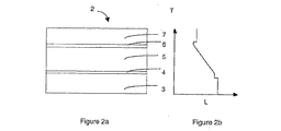
図2aは、図1aの構造におけるものと同じ層を含み、基板上にLaN単層4も含み、さらにターゲット層7の直下に定組成の窒化ランタンスカンジウム合金からなる副層6を含む、第2の結晶構造を示している。ある応用例では、バッファ層が基板上に直に設けられた最初の副層を含むと有利である。この副層は、通常深さが1〜2nmで、より大きな格子定数の元素からなる窒化物のみを通常含む。このような副層は、基板の結晶形となって現れる仮像開始層(pseudomorphic initiation layer)を提供することができる。したがって、LaScN合金のバッファ層の場合、その副層内で純粋なLaNを使用することができる。その後、傾斜バッファ層の成長によって徐々に歪みを増加させることができる。
2a includes the same layers as in the structure of FIG. 1a, includes a LaN
本発明のバッファ構造は、シリコン基板のSi(111)表面に成長させることが理想的である。これによってGaNの場合、六方晶のGaNの成長に適切な対称性を有するテンプレートが提供される。あるいは、ペロブスカイト酸化物またはせん亜鉛鉱型GaN、InN、AlNおよびそれらの合金など、立方型の材料の成長にSi(001)表面を使用することもできる。選択された平面の理想的な配向からの小さなオフカットを有するバッファ層を成長させることもできる。その配向は、例えば、最大5°、好ましくは最大1または2°であるが、ある場合には0.1または0.5°以下のより小さな角度が有用であることもある。このようなオフカットによって、バッファ層およびターゲット材の成長メカニズムを調整して表面形態などの特性を改善することができる。 The buffer structure of the present invention is ideally grown on the Si (111) surface of the silicon substrate. This provides in the case of GaN a template with appropriate symmetry for the growth of hexagonal GaN. Alternatively, the Si (001) surface can be used for growth of cubic materials such as perovskite oxide or zinc-blende GaN, InN, AlN and their alloys. It is also possible to grow buffer layers with small offcuts from the ideal orientation of the selected plane. The orientation is, for example, up to 5 °, preferably up to 1 or 2 °, but in some cases smaller angles of 0.1 or 0.5 ° or less may be useful. By such an offcut, characteristics such as surface morphology can be improved by adjusting the growth mechanism of the buffer layer and the target material.
III−V族窒化物のAlN、InN、GaNおよびそれらの合金を含め、III−V族半導体には、ヘテロエピタキシャルターゲット材として特別な関心が寄せられている。こうした材料の特性によって赤から紫外の波長範囲にわたる効率の良い発光体を生成することができ、高出力、高電圧の電子機器の提供も行われる。したがってターゲット材は、好ましくはIII−V族半導体を含み、より好ましくは窒化アルミニウム、窒化ガリウムまたは窒化インジウム、あるいはそれらの合金を含み、より一層好ましくは、窒化ガリウムを含む。本発明は、ウルツァイト型(六方晶のGaN−最も一般に使用される位相)に特に適した成長表面を提供するものであるが、立方晶(せん亜鉛鉱型)のGaN、ならびに同様に構成されたAlNおよびInN合金も成長させることができる。ScNはさらに重要なターゲット材である。 Group III-V semiconductors, including group III-V nitrides AlN, InN, GaN and their alloys, are of particular interest as heteroepitaxial target materials. Due to the characteristics of these materials, it is possible to produce an efficient light emitter ranging from the red to ultraviolet wavelength range, and to provide high-power, high-voltage electronic devices. Accordingly, the target material preferably includes a III-V semiconductor, more preferably includes aluminum nitride, gallium nitride or indium nitride, or an alloy thereof, and even more preferably includes gallium nitride. The present invention provides a growth surface that is particularly suitable for wurtzite type (hexagonal GaN—the most commonly used phase), but cubic (zincite type) GaN, as well as constructed similarly. AlN and InN alloys can also be grown. ScN is a further important target material.
高い技術的関心が寄せられている別の種類の材料にペロブスカイト構造の酸化物があり、したがって、そのターゲット材はペロブスカイト酸化物を代わりとして含む。こうした酸化物は、例えば、強誘電性、巨大電磁抵抗、高誘電率および圧電性など興味ある一連の材料特性を示し、その特性は全てデバイスに適用することができる。多くのペロブスカイト酸化物は、格子定数がSiより小さいため、バッファ層が質の高いエピタキシャル成長を可能とすることが求められるが、本発明によって達成される格子サイズ内にある。スピネル型構造の酸化物も本発明によって成長させることができる。実行可能なペロブスカイト酸化物ターゲット材の例としては、タンタル酸スカンジウム鉛、チタン酸ジルコニウム鉛、チタン酸ストロンチウム、チタン酸バリウム、マンガン酸ランタンカルシウム、マンガン酸ランタンストロンチウム、マンガン酸ランタンバリウム、ジルコン酸カルシウム、ジルコン酸ストロンチウム、ジルコン酸バリウム、酸化ハフニウム、ケイ酸ハフニウム、ハフニウム酸カルシウム、ハフニウム酸ストロンチウム、およびハフニウム酸バリウムなどがある。 Another type of material that is of high technical interest is perovskite-structured oxides, and therefore the target material includes perovskite oxide instead. Such oxides exhibit an interesting set of material properties such as ferroelectricity, giant electromagnetic resistance, high dielectric constant and piezoelectricity, all of which can be applied to the device. Many perovskite oxides have a lattice constant smaller than Si, so that the buffer layer is required to enable high quality epitaxial growth, but is within the lattice size achieved by the present invention. An oxide having a spinel structure can also be grown according to the present invention. Examples of viable perovskite oxide target materials include lead scandium tantalate, lead zirconium titanate, strontium titanate, barium titanate, lanthanum calcium manganate, lanthanum strontium manganate, lanthanum barium manganate, calcium zirconate, Examples include strontium zirconate, barium zirconate, hafnium oxide, hafnium silicate, calcium hafnate, strontium hafnate, and barium hafnate.
ターゲット材は、バッファ層上に直接成長させることができ、それによって傾斜層の最終的な緩和が行われる。あるいは、バッファ構造はさらに、ターゲット材下方のバッファ層上部に配設された、例えば最大2μのIIIB族窒化物合金からなる定組成層を含むことができ、この層によって材料層の成長前にほぼ完全な格子緩和が強制的に行われる。 The target material can be grown directly on the buffer layer, thereby providing the final relaxation of the graded layer. Alternatively, the buffer structure can further comprise a constant composition layer, for example of up to 2 μm group IIIB nitride alloy, disposed on top of the buffer layer below the target material, with this layer approximately before the material layer is grown. Complete lattice relaxation is forced.
ターゲット材は、所望の電子および機械特性を有する少なくとも1つのデバイス層を形成することができる。ある用途では、同じ材料からなる2つ以上のデバイス層が必要とされることがあり、他の用途では、バッファ層を覆って、互いに異なる材料からなる2つ以上のデバイス層を堆積させることがある。任意選択で、バッファ層の最上領域または副層をターゲット材の格子定数よりわずかに超える格子定数(例えば、最大2%超)に傾斜させることによって、選択された成長温度でターゲット材を圧縮歪み下に置く。実際は、最上領域は、例えば最大1μの固定された組成の窒化物合金からなる、必要とされるわずかに小さな格子定数を有する副層を含むことができる。このように、バッファ層の外面と材料層との間の格子定数の小さな差を利用して、冷却後すぐに圧縮歪みに対し、Siとターゲット材との間の不利益な熱膨張不整合を相殺することが可能である。例えば、ScNはGaNよりもわずかに小さい格子定数を有するが、ある程度の圧縮ひずみを導入することによって、SiとGaNの間の熱不整合による引張り歪みが低減され、それによってターゲット層の割れの可能性が低減される。 The target material can form at least one device layer having desired electronic and mechanical properties. In some applications, two or more device layers of the same material may be required, and in other applications, two or more device layers of different materials may be deposited over the buffer layer. is there. Optionally, the target material is under compressive strain at the selected growth temperature by tilting the top region or sublayer of the buffer layer to a lattice constant that is slightly greater than the lattice constant of the target material (eg, greater than 2% maximum). Put on. In practice, the top region may comprise a sublayer with a slightly smaller lattice constant required, for example made of a fixed composition nitride alloy of up to 1 μm. In this way, a small difference in lattice constant between the outer surface of the buffer layer and the material layer is used to provide a detrimental thermal expansion mismatch between Si and the target material against compressive strain immediately after cooling. It is possible to cancel. For example, ScN has a slightly smaller lattice constant than GaN, but by introducing a certain amount of compressive strain, tensile strain due to thermal mismatch between Si and GaN is reduced, thereby allowing the target layer to crack Is reduced.
IIIB族窒化物は、エピ層と基板の間の原子種の相互拡散を防止するバリア層としてある程度作用することができる。さらに、IIIB族窒化物は、知られている様々なエピタキシャル成長プロセスを使用して堆積させることができ、比較的高い融点を有するので、GaNなど通常必要とされるターゲット材に必要な後続の成長条件との適合性を提供することができる。次の例では、分子線エピタキシ(MBE)を使用してバッファ構造を設けている。しかし、バッファ構造は、例えば、金属有機分子線エピタキシ(MOMBE)、金属有機気相成長(MOCVD)、プラズマ促進気相成長(PEPVD)、化学ビームエピタキシ(CBE)、液相エピタキシ(LPE)またはエピタキシャル成長に適していると知られている他の技法を使用しても成長させることができる。技法は、バッファ構造とターゲット材とが同じ装置を使用し、好ましくは単一のプロセスで堆積させることができるように選択されることが好ましい。したがって、LaN、ScNおよびYNは全て水素ベースの前駆体から成長させることができるので、GaN合金からなるターゲット材の場合、MOCVDをうまく使用することができる。 The IIIB nitride can act to some extent as a barrier layer that prevents interdiffusion of atomic species between the epi layer and the substrate. Further, IIIB nitrides can be deposited using a variety of known epitaxial growth processes and have a relatively high melting point, so that subsequent growth conditions required for normally required target materials such as GaN. Can provide compatibility. In the following example, a buffer structure is provided using molecular beam epitaxy (MBE). However, the buffer structure may be, for example, metal organic molecular beam epitaxy (MOMBE), metal organic vapor deposition (MOCVD), plasma enhanced vapor deposition (PEPVD), chemical beam epitaxy (CBE), liquid phase epitaxy (LPE) or epitaxial growth. Other techniques known to be suitable for can also be used for growth. The technique is preferably selected so that the buffer structure and the target material can be deposited using the same apparatus, preferably in a single process. Therefore, since LaN, ScN and YN can all be grown from hydrogen-based precursors, MOCVD can be successfully used for target materials made of GaN alloys.
本発明によるバッファ構造は、電子工学、光電子工学、MEMS、フォトニクス、センサおよび画像を含む技術分野における様々なデバイスの応用例において使用することができる。したがって、さらなる態様では、本発明は上記の結晶構造/バッファ構造を含む半導体を提供する。デバイスは、LED、レーザダイオード、トランジスタなどを含む通常の用途の光学電子デバイスでよい。 The buffer structure according to the present invention can be used in various device applications in the technical field including electronics, optoelectronics, MEMS, photonics, sensors and images. Accordingly, in a further aspect, the present invention provides a semiconductor comprising the crystal structure / buffer structure described above. The device may be an optoelectronic device for normal use including LEDs, laser diodes, transistors, and the like.
本発明は、その表面の一部上で領域選択エピタキシ(selective area epitaxy)によって成長させた本発明による1つまたは複数のバッファ構造を含むシリコン基板、例えばシリコンウェハをさらに提供する。次いで、このようなバッファ構造およびそれに関連するターゲット材層は、シリコン基板/ウェハの残り部分上にパターニングされたシリコンデバイスに一体化することができる。 The present invention further provides a silicon substrate, eg, a silicon wafer, comprising one or more buffer structures according to the present invention grown by selective area epitaxy on a portion of its surface. Such a buffer structure and its associated target material layer can then be integrated into a silicon device patterned on the remainder of the silicon substrate / wafer.
デバイスは普通、ターゲット材、バッファ層およびシリコン基板を含むが、例えば、本発明のバッファ層がそれ自体、デバイスの底部コンタクトとしての役割を果たすようになっている場合、シリコン基板は後に削除(したがって、単にテンプレートとしての役割を果たす)される応用例もあり得る。 A device typically includes a target material, a buffer layer, and a silicon substrate, but if the buffer layer of the present invention is itself intended to serve as the bottom contact of the device, the silicon substrate is later deleted (and thus There may be applications that simply serve as templates.
さらなる態様では、本発明は、本発明の方法を使用して得られた単結晶ターゲット材を提供する。この材料は、バッファ層から分離されている。単結晶材料は、半導体または他の様々な用途に使用することができ、こうした用途に適した材料を形成するためにドープすることができる。 In a further aspect, the present invention provides a single crystal target material obtained using the method of the present invention. This material is separated from the buffer layer. Single crystal materials can be used for semiconductor or various other applications and can be doped to form materials suitable for such applications.
以下の例において、La/Sc窒化物合金からなる傾斜バッファ層を含む、本発明によるバッファ構造を作成する1つの方法の一例を説明する。 In the following example, an example of one method for creating a buffer structure according to the present invention comprising a gradient buffer layer made of La / Sc nitride alloy will be described.
標準の湿式化学プロセスである真空除去(ex−vacuo)を使用してSi基板から自然酸素がまず除去され、調整を利かせたやり方で、Si基板上に希薄で均一な自然酸素が再形成された。基板はMBE室に装入され、再形成された自然酸素を熱的に取り除くために約950℃で30分間加熱され、その結果、清浄な(7×7)構造の再構成(111)Si表面を得た。 Natural oxygen is first removed from the Si substrate using a standard wet chemical process, ex-vacuo, and in a controlled manner, lean and uniform natural oxygen is re-formed on the Si substrate. It was. The substrate is loaded into the MBE chamber and heated at about 950 ° C. for 30 minutes to thermally remove the regenerated natural oxygen, resulting in a reconstructed (111) Si surface with a clean (7 × 7) structure Got.
予備処理されたSi基板は、700℃に冷却され、エフュージョンセルを使用し、典型的な0.3ml/秒のLa流量および10−7トルのバックグラウンド圧で、(Si基板の窒化物形成を防止するように)La金属からなる1枚から2枚の単層がSi表面上に堆積された。MBE室のバックグラウンド圧は次いで、ブリージングによって窒素内で5×10−6トルに増大され、La単層は、高周波のプラズマ窒素源を使用し、出力を500Wに設定して窒化物に変換された。 The pre-treated Si substrate was cooled to 700 ° C., using an effusion cell, with a typical 0.3 ml / s La flow rate and 10 −7 Torr background pressure (Si substrate nitridation). One to two monolayers of La metal were deposited on the Si surface (to prevent). The MBE chamber background pressure was then increased to 5 × 10 −6 Torr in nitrogen by breathing, and the La monolayer was converted to nitride using a high frequency plasma nitrogen source and setting the power to 500 W. It was.
Laシャッタが再開されて厚さが1〜2nmのLaN層の成長が開始され、次いでScシャッタも開かれた。LaセルおよびScセルを反対に傾斜させることによって、1ミクロン当たり約x=0.5の傾斜率でLa(1−x)ScxNの組成傾斜層の成長が開始された。Scセルの開始流量は0.003ml/秒であった。傾斜層の堆積中、基板温度が700℃から900℃に傾斜され窒素の豊富な状態が維持された。 The La shutter was restarted and the growth of the LaN layer with a thickness of 1 to 2 nm was started, and then the Sc shutter was also opened. By tilting the La and Sc cells in opposition, growth of a compositionally graded layer of La (1-x) Sc x N was initiated at a ramp rate of about x = 0.5 per micron. The starting flow rate of the Sc cell was 0.003 ml / sec. During the deposition of the graded layer, the substrate temperature was ramped from 700 ° C. to 900 ° C. to maintain a nitrogen rich state.
傾斜は、所望のターゲット材に関して適切な格子定数を提供する組成のところで停止された。この例では、後続のGaN堆積のための格子整合を提供するために、La(1−x)ScxN層の傾斜はLa0.07Sc0.93Nの組成のところで停止され、次いで膜を完全に緩和するように0.5μのLaScNの定組成層が堆積された。 The tilt was stopped at a composition that provided the appropriate lattice constant for the desired target material. In this example, the La (1-x) Sc x N layer tilt is stopped at the composition of La 0.07 Sc 0.93 N and then the film to provide lattice matching for subsequent GaN deposition. A 0.5 μm LaScN isocratic layer was deposited to completely relax.
次いで、従来のMOCVDプロセスを使用してGaNのターゲット材層が堆積された。 A GaN target material layer was then deposited using a conventional MOCVD process.
Claims (15)
Applications Claiming Priority (2)
| Application Number | Priority Date | Filing Date | Title |
|---|---|---|---|
| GB0303784A GB2398672A (en) | 2003-02-19 | 2003-02-19 | Group IIIA nitride buffer layers |
| PCT/GB2004/000560 WO2004075249A2 (en) | 2003-02-19 | 2004-02-16 | Buffer structure for modifying a silicon substrate |
Publications (3)
| Publication Number | Publication Date |
|---|---|
| JP2006518104A JP2006518104A (en) | 2006-08-03 |
| JP2006518104A5 JP2006518104A5 (en) | 2007-03-15 |
| JP4493646B2 true JP4493646B2 (en) | 2010-06-30 |
Family
ID=9953280
Family Applications (1)
| Application Number | Title | Priority Date | Filing Date |
|---|---|---|---|
| JP2006502270A Expired - Fee Related JP4493646B2 (en) | 2003-02-19 | 2004-02-16 | Buffer structure for modifying a silicon substrate for subsequent target material deposition and method of forming the buffer structure |
Country Status (8)
| Country | Link |
|---|---|
| US (1) | US7323764B2 (en) |
| EP (1) | EP1595280B8 (en) |
| JP (1) | JP4493646B2 (en) |
| CN (1) | CN100382244C (en) |
| AT (1) | ATE349774T1 (en) |
| DE (1) | DE602004003910T2 (en) |
| GB (2) | GB2398672A (en) |
| WO (1) | WO2004075249A2 (en) |
Families Citing this family (31)
| Publication number | Priority date | Publication date | Assignee | Title |
|---|---|---|---|---|
| EP1883103A3 (en) * | 2006-07-27 | 2008-03-05 | Interuniversitair Microelektronica Centrum | Deposition of group III-nitrides on Ge |
| US7494911B2 (en) | 2006-09-27 | 2009-02-24 | Intel Corporation | Buffer layers for device isolation of devices grown on silicon |
| US8106381B2 (en) * | 2006-10-18 | 2012-01-31 | Translucent, Inc. | Semiconductor structures with rare-earths |
| US8157914B1 (en) | 2007-02-07 | 2012-04-17 | Chien-Min Sung | Substrate surface modifications for compositional gradation of crystalline materials and associated products |
| US7799600B2 (en) | 2007-05-31 | 2010-09-21 | Chien-Min Sung | Doped diamond LED devices and associated methods |
| US8049100B2 (en) * | 2007-07-26 | 2011-11-01 | Translucent, Inc. | Multijunction rare earth solar cell |
| US8039737B2 (en) * | 2007-07-26 | 2011-10-18 | Translucent, Inc. | Passive rare earth tandem solar cell |
| US8039738B2 (en) * | 2007-07-26 | 2011-10-18 | Translucent, Inc. | Active rare earth tandem solar cell |
| EP2250674A4 (en) * | 2008-01-28 | 2013-02-13 | Amit Goyal | Semiconductor-based large-area flexible electronic devices |
| DE102009000514A1 (en) * | 2009-01-30 | 2010-08-26 | Robert Bosch Gmbh | Composite component and method for producing a composite component |
| CN102714145B (en) * | 2009-03-27 | 2015-07-08 | 同和控股(集团)有限公司 | Substrate for growing group-III nitride semiconductors, epitaxial substrate for group- III nitride semiconductors, group- III nitride semiconductor element, stand-alone substrate for group- III nitride semiconductors, and methods for manufacturing the preceding |
| GB2469448A (en) * | 2009-04-14 | 2010-10-20 | Qinetiq Ltd | Strain Control in Semiconductor Devices |
| JP5614531B2 (en) * | 2010-03-12 | 2014-10-29 | セイコーエプソン株式会社 | Liquid ejecting head, liquid ejecting apparatus using the same, and piezoelectric element |
| US9041027B2 (en) | 2010-12-01 | 2015-05-26 | Alliance For Sustainable Energy, Llc | Methods of producing free-standing semiconductors using sacrificial buffer layers and recyclable substrates |
| WO2012074524A1 (en) | 2010-12-01 | 2012-06-07 | Alliance For Sustainable Energy, Llc | Coincident site lattice-matched growth of semiconductors on substrates using compliant buffer layers |
| KR101883840B1 (en) * | 2011-08-31 | 2018-08-01 | 엘지이노텍 주식회사 | Light emitting diode |
| US9012921B2 (en) | 2011-09-29 | 2015-04-21 | Kabushiki Kaisha Toshiba | Light emitting devices having light coupling layers |
| US8698163B2 (en) | 2011-09-29 | 2014-04-15 | Toshiba Techno Center Inc. | P-type doping layers for use with light emitting devices |
| US9178114B2 (en) | 2011-09-29 | 2015-11-03 | Manutius Ip, Inc. | P-type doping layers for use with light emitting devices |
| US8664679B2 (en) | 2011-09-29 | 2014-03-04 | Toshiba Techno Center Inc. | Light emitting devices having light coupling layers with recessed electrodes |
| US20130082274A1 (en) | 2011-09-29 | 2013-04-04 | Bridgelux, Inc. | Light emitting devices having dislocation density maintaining buffer layers |
| US8853668B2 (en) | 2011-09-29 | 2014-10-07 | Kabushiki Kaisha Toshiba | Light emitting regions for use with light emitting devices |
| US20130099357A1 (en) * | 2011-10-21 | 2013-04-25 | Rytis Dargis | Strain compensated reo buffer for iii-n on silicon |
| US8394194B1 (en) * | 2012-06-13 | 2013-03-12 | Rytis Dargis | Single crystal reo buffer on amorphous SiOx |
| CN104641453B (en) * | 2012-10-12 | 2018-03-30 | 住友电气工业株式会社 | Group III nitride composite substrate and its manufacture method and the method for manufacturing Group III nitride semiconductor device |
| CN103794460B (en) * | 2012-10-29 | 2016-12-21 | 中微半导体设备(上海)有限公司 | The coating improved for performance of semiconductor devices |
| TWI491068B (en) * | 2012-11-08 | 2015-07-01 | Ind Tech Res Inst | Nitride semiconductor structure |
| CN105393336B (en) * | 2013-07-22 | 2017-10-31 | 日本碍子株式会社 | Composite base plate, its manufacture method, function element and crystal seed substrate |
| TWI753915B (en) * | 2016-06-02 | 2022-02-01 | 英商Iqe有限公司 | PNICTIDE BUFFER STRUCTURES AND DEVICES FOR GaN BASE APPLICATIONS |
| KR102098572B1 (en) * | 2018-12-26 | 2020-04-08 | 한국세라믹기술원 | Substrate Material Searching Apparatus and Method for Epitaxy Growth and Record Media Recorded Program for Realizing the Same |
| US20240084479A1 (en) * | 2021-01-19 | 2024-03-14 | Alliance For Sustainable Energy, Llc | Dynamic hvpe of compositionally graded buffer layers |
Family Cites Families (15)
| Publication number | Priority date | Publication date | Assignee | Title |
|---|---|---|---|---|
| JPS50102581A (en) * | 1974-01-16 | 1975-08-13 | ||
| US5393993A (en) | 1993-12-13 | 1995-02-28 | Cree Research, Inc. | Buffer structure between silicon carbide and gallium nitride and resulting semiconductor devices |
| JP3557011B2 (en) * | 1995-03-30 | 2004-08-25 | 株式会社東芝 | Semiconductor light emitting device and manufacturing method thereof |
| JP3813740B2 (en) * | 1997-07-11 | 2006-08-23 | Tdk株式会社 | Substrates for electronic devices |
| US6201262B1 (en) | 1997-10-07 | 2001-03-13 | Cree, Inc. | Group III nitride photonic devices on silicon carbide substrates with conductive buffer interlay structure |
| JP3853942B2 (en) * | 1997-11-12 | 2006-12-06 | 昭和電工株式会社 | Epitaxial wafer |
| US6171898B1 (en) * | 1997-12-17 | 2001-01-09 | Texas Instruments Incorporated | Method of fabricating an oxygen-stable layer/diffusion barrier/poly bottom electrode structure for high-K-DRAMS using a disposable-oxide processing |
| US5998232A (en) * | 1998-01-16 | 1999-12-07 | Implant Sciences Corporation | Planar technology for producing light-emitting devices |
| US6255198B1 (en) | 1998-11-24 | 2001-07-03 | North Carolina State University | Methods of fabricating gallium nitride microelectronic layers on silicon layers and gallium nitride microelectronic structures formed thereby |
| JP2001230447A (en) * | 2000-02-16 | 2001-08-24 | Toyoda Gosei Co Ltd | Manufacture method for iii nitride-based compound semiconductor element |
| US6649287B2 (en) * | 2000-12-14 | 2003-11-18 | Nitronex Corporation | Gallium nitride materials and methods |
| JP3785059B2 (en) * | 2001-06-25 | 2006-06-14 | 宣彦 澤木 | Manufacturing method of nitride semiconductor |
| US6646293B2 (en) * | 2001-07-18 | 2003-11-11 | Motorola, Inc. | Structure for fabricating high electron mobility transistors utilizing the formation of complaint substrates |
| US6472694B1 (en) * | 2001-07-23 | 2002-10-29 | Motorola, Inc. | Microprocessor structure having a compound semiconductor layer |
| JP2002222803A (en) * | 2001-12-03 | 2002-08-09 | Kyocera Corp | Corrosion resistant member for manufacturing semiconductor |
-
2003
- 2003-02-19 GB GB0303784A patent/GB2398672A/en not_active Withdrawn
-
2004
- 2004-02-16 DE DE602004003910T patent/DE602004003910T2/en not_active Expired - Lifetime
- 2004-02-16 GB GB0515760A patent/GB2413898B/en not_active Expired - Fee Related
- 2004-02-16 WO PCT/GB2004/000560 patent/WO2004075249A2/en active IP Right Grant
- 2004-02-16 US US10/545,911 patent/US7323764B2/en not_active Expired - Lifetime
- 2004-02-16 AT AT04711402T patent/ATE349774T1/en not_active IP Right Cessation
- 2004-02-16 JP JP2006502270A patent/JP4493646B2/en not_active Expired - Fee Related
- 2004-02-16 EP EP04711402A patent/EP1595280B8/en not_active Expired - Lifetime
- 2004-02-16 CN CNB2004800046781A patent/CN100382244C/en not_active Expired - Fee Related
Also Published As
| Publication number | Publication date |
|---|---|
| DE602004003910D1 (en) | 2007-02-08 |
| GB2398672A (en) | 2004-08-25 |
| ATE349774T1 (en) | 2007-01-15 |
| GB0303784D0 (en) | 2003-03-26 |
| US20060145186A1 (en) | 2006-07-06 |
| EP1595280A2 (en) | 2005-11-16 |
| US7323764B2 (en) | 2008-01-29 |
| CN1751379A (en) | 2006-03-22 |
| GB0515760D0 (en) | 2005-09-07 |
| JP2006518104A (en) | 2006-08-03 |
| GB2413898B (en) | 2006-08-16 |
| CN100382244C (en) | 2008-04-16 |
| DE602004003910T2 (en) | 2007-05-16 |
| GB2413898A (en) | 2005-11-09 |
| EP1595280B8 (en) | 2007-02-28 |
| WO2004075249A3 (en) | 2004-10-28 |
| EP1595280B1 (en) | 2006-12-27 |
| WO2004075249A2 (en) | 2004-09-02 |
Similar Documents
| Publication | Publication Date | Title |
|---|---|---|
| JP4493646B2 (en) | Buffer structure for modifying a silicon substrate for subsequent target material deposition and method of forming the buffer structure | |
| US7811902B2 (en) | Method for manufacturing nitride based single crystal substrate and method for manufacturing nitride based light emitting diode using the same | |
| KR100897589B1 (en) | Preparation method of a coating of gallium nitride | |
| JP5842057B2 (en) | Manufacturing method of semiconductor device | |
| US6255198B1 (en) | Methods of fabricating gallium nitride microelectronic layers on silicon layers and gallium nitride microelectronic structures formed thereby | |
| RU2470412C2 (en) | Method of making light-emitting devices based on group iii nitrides grown on stress relief templates | |
| KR101899742B1 (en) | Semiconductor structure comprising an active semiconductor layer of the iii-v type on a buffer layer stack and method for producing semiconductor structure | |
| US8283673B2 (en) | Method for manufacturing a layer of gallium nitride or gallium and aluminum nitride | |
| TW200419652A (en) | Growth of reduced dislocation density non-polar gallium nitride by hydride vapor phase epitaxy | |
| JP2008504715A (en) | Gallium nitride materials and methods | |
| JP2004508268A (en) | Method of forming a defect-free, crack-free epitaxial film on a mismatched substrate | |
| TW201443990A (en) | Technique for the growth of planar semi-polar gallium nitride | |
| JP2005303246A (en) | METHOD OF GROWING HIGH QUALITY ZnSe EPITAXIAL LAYER ONTO NEW Si SUBSTRATE | |
| KR101892610B1 (en) | III-V semiconductor structures and methods for forming the same | |
| JP2009524251A (en) | Method for promoting the growth of semipolar (Al, In, Ga, B) N via metalorganic chemical vapor deposition | |
| US7361522B2 (en) | Growing lower defect semiconductor crystals on highly lattice-mismatched substrates | |
| CN102246291A (en) | Strain engineered composite semiconductor substrates and methods of forming same | |
| WO2013145404A1 (en) | Laminated substate of silicon single crystal and group iii nitride single crystal with off angle | |
| EP2362412B1 (en) | Method of growing nitride semiconductor | |
| JPH10303510A (en) | Iii-group nitride semiconductor device and its manufacture | |
| KR20180120193A (en) | Method for obtaining a semi-polar nitride layer on a crystalline substrate | |
| Li et al. | Metalorganic chemical vapour deposition (MOCVD) growth of GaN on foundry compatible 200 mm Si | |
| Thapa et al. | Semiconductor wafer with a layer of Al z Ga 1-z N and process for producing it | |
| JPH11219904A (en) | Compound semiconductor substrate and manufacture of the same, and compound semiconductor light-emitting element | |
| SOMOGYI¹ et al. | A COMPARISON OF GALVANOMAGNETIC PROPERTIES OF GaN EPITAXIAL LAYERS GROWN ON SILICON AND SAPPHIRE SUBSTRATES |
Legal Events
| Date | Code | Title | Description |
|---|---|---|---|
| A521 | Request for written amendment filed |
Free format text: JAPANESE INTERMEDIATE CODE: A523 Effective date: 20070124 |
|
| A621 | Written request for application examination |
Free format text: JAPANESE INTERMEDIATE CODE: A621 Effective date: 20070124 |
|
| A977 | Report on retrieval |
Free format text: JAPANESE INTERMEDIATE CODE: A971007 Effective date: 20091112 |
|
| A131 | Notification of reasons for refusal |
Free format text: JAPANESE INTERMEDIATE CODE: A131 Effective date: 20091117 |
|
| A521 | Request for written amendment filed |
Free format text: JAPANESE INTERMEDIATE CODE: A523 Effective date: 20100217 |
|
| TRDD | Decision of grant or rejection written | ||
| A01 | Written decision to grant a patent or to grant a registration (utility model) |
Free format text: JAPANESE INTERMEDIATE CODE: A01 Effective date: 20100316 |
|
| A01 | Written decision to grant a patent or to grant a registration (utility model) |
Free format text: JAPANESE INTERMEDIATE CODE: A01 |
|
| A61 | First payment of annual fees (during grant procedure) |
Free format text: JAPANESE INTERMEDIATE CODE: A61 Effective date: 20100406 |
|
| R150 | Certificate of patent or registration of utility model |
Free format text: JAPANESE INTERMEDIATE CODE: R150 |
|
| FPAY | Renewal fee payment (event date is renewal date of database) |
Free format text: PAYMENT UNTIL: 20130416 Year of fee payment: 3 |
|
| R250 | Receipt of annual fees |
Free format text: JAPANESE INTERMEDIATE CODE: R250 |
|
| LAPS | Cancellation because of no payment of annual fees |