JP4489113B2 - Resonator and filter - Google Patents
Resonator and filter Download PDFInfo
- Publication number
- JP4489113B2 JP4489113B2 JP2007304571A JP2007304571A JP4489113B2 JP 4489113 B2 JP4489113 B2 JP 4489113B2 JP 2007304571 A JP2007304571 A JP 2007304571A JP 2007304571 A JP2007304571 A JP 2007304571A JP 4489113 B2 JP4489113 B2 JP 4489113B2
- Authority
- JP
- Japan
- Prior art keywords
- resonator
- conductor line
- slit
- line
- bent portion
- Prior art date
- Legal status (The legal status is an assumption and is not a legal conclusion. Google has not performed a legal analysis and makes no representation as to the accuracy of the status listed.)
- Active
Links
Images


Classifications
-
- H—ELECTRICITY
- H01—ELECTRIC ELEMENTS
- H01P—WAVEGUIDES; RESONATORS, LINES, OR OTHER DEVICES OF THE WAVEGUIDE TYPE
- H01P1/00—Auxiliary devices
- H01P1/20—Frequency-selective devices, e.g. filters
- H01P1/201—Filters for transverse electromagnetic waves
- H01P1/203—Strip line filters
- H01P1/20327—Electromagnetic interstage coupling
- H01P1/20354—Non-comb or non-interdigital filters
- H01P1/20372—Hairpin resonators
-
- H—ELECTRICITY
- H01—ELECTRIC ELEMENTS
- H01P—WAVEGUIDES; RESONATORS, LINES, OR OTHER DEVICES OF THE WAVEGUIDE TYPE
- H01P7/00—Resonators of the waveguide type
- H01P7/08—Strip line resonators
- H01P7/082—Microstripline resonators
Description
本発明は、マイクロ波を利用した装置、例えば、放送機器、通信機器、測定器等に用いられる共振器およびフィルタに関する。 The present invention relates to a resonator and a filter used in a device using a microwave, for example, a broadcasting device, a communication device, a measuring instrument, and the like.
ストリップラインもしくはマイクロストリップライン構造のマイクロ波共振器の中で最も単純な形状の一つは、共振周波数において半波長(180度)もしくは半波長の整数倍の電気長を有する導体線路と誘電体基板および接地板から成る構造の伝送線路で構成される共振器である。この共振器は導体線路に沿って電流が流れるモードで共振し、共振状態での電流密度分布は導体線路のエッジ部分に最も集中し、この傾向は周波数が高くなるほど顕著である。 One of the simplest shapes of microwave resonators having a stripline or microstripline structure is a conductor line and a dielectric substrate having an electrical length of a half wavelength (180 degrees) or an integral multiple of a half wavelength at the resonance frequency. And a resonator including a transmission line having a structure including a ground plate. This resonator resonates in a mode in which current flows along the conductor line, and the current density distribution in the resonance state is most concentrated at the edge portion of the conductor line, and this tendency becomes more prominent as the frequency increases.
前述のようなタイプの共振器を、例えば1W以上といった、大電力信号用のマイクロ波共振器として利用する場合には、エッジ部分への電流集中が問題となる。これは、大電力信号によって導体線路のエッジ部分に特に大きな電流密度が生じ、結果としてエッジ部分の導体損失が共振器の損失特性の支配的要因となるためである。また、その大きな電流密度が導体材料の許容電流密度を超えることで、導体材料の電気伝導特性が破壊される場合もある。例えば、超電導材料を用いて導体線路を形成している場合に、エッジ部分の電流密度が超電導材料の臨界電流密度を超えた場合などがこれに該当する。 When a resonator of the type described above is used as a microwave resonator for a high power signal such as 1 W or more, current concentration at the edge becomes a problem. This is because a large power density causes a particularly large current density at the edge portion of the conductor line, and as a result, the conductor loss at the edge portion becomes a dominant factor in the loss characteristics of the resonator. In addition, when the large current density exceeds the allowable current density of the conductor material, the electric conduction characteristics of the conductor material may be destroyed. For example, when the conductor line is formed using a superconducting material, the case where the current density of the edge portion exceeds the critical current density of the superconducting material corresponds to this.
導体線路のエッジ部分の電流集中を緩和する方法としては、直線型の導体線路全体に導体線路に沿って均一の間隔で複数本のスリットを設ける方法が、特許文献1において提案されている。また、この方法をさらに改良した方法として、直線型の導体線路のエッジ部分のみに導体線路に沿って単数もしくは複数本のスリットを設ける方法が、特許文献2において提案されている。
As a method for alleviating the current concentration at the edge portion of the conductor line,
また、導体線路の形状は、直線が最も単純ではあるが、限られた基板サイズの中に共振器を納める等の理由から、ヘアピン型、スパイラル型、メアンダ型、L字型、M字型、S字型など単数もしくは複数の、屈曲または湾曲した曲がり部を有する様々な形状が考案されている。
ストリップラインもしくはマイクロストリップライン構造の伝送線路を共振器として用いる場合に、その導体線路の形状が直線型の場合には上記特許文献1または特許文献2の方法が有効である。しかし、導体線路が曲がり部を有する場合には新たな問題が生じうることに発明者らは着目した。それは導体線路の曲がり部内側のエッジ部分への電流集中である。
When a transmission line having a stripline or microstripline structure is used as a resonator and the shape of the conductor line is a straight line, the method of
本発明は、上記事情を考慮してなされたものであり、その目的とするところは、導体線路の曲がり部内側と外側の電流分布の不均衡を解消し、低損失かつ高耐電力の共振器およびフィルタを提供することにある。 The present invention has been made in consideration of the above-mentioned circumstances, and an object of the present invention is to eliminate a current distribution imbalance between the inside and outside of the bent portion of the conductor line, and to achieve a low-loss and high-power-resistant resonator. And providing a filter.
本発明の一態様の共振器は、曲がり部を有する導体線路を備える伝送線路で構成される共振器であって、前記伝送線路がストリップライン構造またはマイクロストリップライン構造を有し、前記導体線路の前記曲がり部に、前記導体線路の伸長方向に沿った複数本のスリットが設けられ、前記スリット間にある線路の線幅が、前記曲がり部の外側から内側に向かうに従って細くなっていることを特徴とする。
A resonator according to one embodiment of the present invention is a resonator including a transmission line including a conductor line having a bent portion, and the transmission line has a stripline structure or a microstripline structure. The bent portion is provided with a plurality of slits along the extending direction of the conductor line, and the line width of the line between the slits becomes narrower from the outside to the inside of the bent portion. And
ここで、前記導体線路の両縁端部には、前記スリットが設けられていないことが望ましい。 Here, it is desirable that the slits are not provided at both end portions of the conductor line.
ここで、前記スリットの長さが、前記共振器の共振周波数における電気長にして45度以上90度以下であって、前記スリットの長さ方向の略中央部が、前記曲がり部の略中央部に一致することが望ましい。 Here, the length of the slit is not less than 45 degrees and not more than 90 degrees in terms of the electrical length at the resonance frequency of the resonator, and the substantially central portion in the length direction of the slit is substantially the central portion of the bent portion. It is desirable to match.
ここで、前記導体線路がコの字形状を有することが望ましい。 Here, it is desirable that the conductor line has a U-shape.
ここで、前記導体線路がU字形状を有することが望ましい。 Here, it is desirable that the conductor line has a U shape.
ここで、前記導体線路が超電導体で形成されていることが望ましい。 Here, it is desirable that the conductor line is formed of a superconductor.
本発明の一態様のフィルタは、上記態様の共振器を用いて構成されることを特徴とする。 The filter of one embodiment of the present invention is formed using the resonator of the above embodiment.
本発明によれば、導体線路の曲がり部内側と外側の電流分布の不均衡を解消し、低損失かつ高耐電力の共振器およびフィルタを提供することが可能となる。 ADVANTAGE OF THE INVENTION According to this invention, it becomes possible to eliminate the imbalance of the current distribution inside and outside the bent portion of the conductor line, and to provide a resonator and filter with low loss and high power resistance.
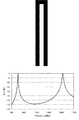
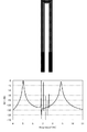
上述のように、導体線路が曲がり部を有する場合には、導体線路の曲がり部内側のエッジ部分への電流集中という新たな問題が生じうることに発明者らは着目し、検討を行った。図29は、直線型の導体線路における電流集中の説明図である。図に示したように、直線型の導体線路90の場合にはエッジ部分に電流が集中するものの、導体線路90の線路中央に沿った軸92に関しては対称に電流が分布する。
As described above, when the conductor line has a bent portion, the inventors have paid attention to the fact that a new problem of current concentration on the edge portion inside the bent portion of the conductor line may occur. FIG. 29 is an explanatory diagram of current concentration in a linear conductor line. As shown in the figure, in the case of the
図30は、スリットを設けた直線型の導体線路における電流集中の説明図である。図に示したように、線路中央に沿った軸92に対して対称なスリット構造を導体線路90に設けることによって、電流密度分布を均一化(左右の電流のピーク値が同じ)することができる。
FIG. 30 is an explanatory diagram of current concentration in a linear conductor line provided with a slit. As shown in the figure, by providing the
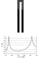
図31は、スリットを設けた曲がり部を有する導体線路における電流集中の説明図である。図に示したように、導体線路90に曲がり部が有る場合には、曲がり部の内側と外側とで電流分布が不均一となる。このため、線路中央に沿った軸92に対して対称なスリット構造を設けるだけでは、図31のグラフ中最も右側のピークに見られるように、導体線路の曲がり部内側のエッジ部分への電流集中を解消することができない。この部分の大きな電流密度が共振器の損失特性や耐電力性を制限する要因となる。
FIG. 31 is an explanatory diagram of current concentration in a conductor line having a bent portion provided with a slit. As shown in the figure, when the
したがって、導体線路の曲がり部内側のエッジ部分への電流集中を解消する技術が必要となる。以下、図面を参照しつつ、導体線路の曲がり部内側のエッジ部分への電流集中を解消する本発明の実施の形態について説明する。 Therefore, a technique for eliminating current concentration at the edge portion inside the bent portion of the conductor line is required. Hereinafter, an embodiment of the present invention that eliminates current concentration at an edge portion inside a bent portion of a conductor line will be described with reference to the drawings.
(第1の実施の形態)
本発明の第1の実施の形態の共振器は、曲がり部を有する導体線路を備える伝送線路で構成される共振器であって、伝送線路がマイクロストリップライン構造を有し、導体線路の曲がり部に、導体線路の伸長方向に沿った複数本のスリットが設けられ、スリット間の間隔が、曲がり部の内側ほど狭いことを特徴とする。
(First embodiment)
The resonator according to the first embodiment of the present invention is a resonator composed of a transmission line including a conductor line having a bent portion, the transmission line having a microstrip line structure, and the bent portion of the conductor line. In addition, a plurality of slits are provided along the extending direction of the conductor line, and the interval between the slits is narrower toward the inside of the bent portion.
このように、曲がり部の内側ほど狭いスリットを伝送線路に設けることにより、曲がり部内側でエッジ部分への電流集中が防止可能となり、共振器の耐電力性を向上させるとともに電力損失も低減することが可能となる。 In this way, by providing the transmission line with a narrower slit toward the inner side of the bent part, it is possible to prevent current concentration on the edge part inside the bent part, improving the power durability of the resonator and reducing power loss. Is possible.
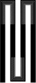
図1は、本実施の形態の共振器の導体線路パターンを示す平面図である。本実施の形態の共振器を構成する伝送線路はマイクロストリップライン構造を有している。この図はマイクロストリップライン構造の基板を上面方向から見た図であり、黒塗り部分が導体線路10となっている。導体線路10の形状はヘアピン型、特に、コの字形状を有している。このヘアピン型共振器の屈曲した曲がり部には導体線路10の伸長方向に沿って一方の縁端部付近12からもう一方の縁端部付近14まで5本のスリット20、22、24、26、28が設けられている。スリット20が曲がり部の最も外側のスリットであり、スリット28が最も内側のスリットである。
FIG. 1 is a plan view showing a conductor line pattern of the resonator according to the present embodiment. The transmission line constituting the resonator according to the present embodiment has a microstrip line structure. This figure is a view of a substrate having a microstrip line structure as viewed from above, and the black-painted portion is a
これら5本のスリットのうち隣り合うスリット間の間隔、すなわちスリット間にある線路の線幅は曲がり部の外側から内側に向かうにしたがって狭くなっている。この例においてその間隔は外側から3.4対2.8対2.2対1.6の比率になっている。また、スリットに隔てられた各線路のうちで最も外側の線路30と最も内側の線路32の線幅の比は4対1となっている。
Among these five slits, the interval between adjacent slits, that is, the line width of the line between the slits becomes narrower from the outside to the inside of the bent portion. In this example, the spacing is 3.4: 2.8: 2.2: 1.6 from the outside. Moreover, the ratio of the line widths of the
そして、本実施の形態においては、導体線路10の両縁端部12、14が閉じた構造になっている。すなわち、導体線路10の両縁端部にはスリットが設けられていない。
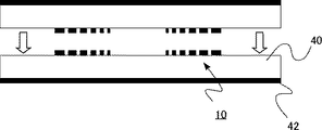
In the present embodiment, both
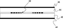
図2は、図1に示した共振器のA−A’断面図である。図1に示した導体線路10が誘電体基板40の上面に形成されている。誘電体基板40の下面には導体材料で接地板(グランドプレーン)42が形成されており、マイクロストリップライン構造となっている。ここで、導体線路10は、例えば超電導材料であるYBCOで形成されている。また、誘電体基板40としては、例えば、サファイアが用いられる。
2 is a cross-sectional view of the resonator shown in FIG. 1 taken along the line A-A ′. The
図3は、図1の共振器のB−B’断面図と、断面における電流密度の分布を示す図である。図3の上のグラフが電流密度の分布であり、縦軸が電流密度を横軸が位置を表している。図31と比較すると、曲がり部内側(B’側)の電流密度が外側とほぼ同じくなるまで均等化されていることが分かる。電磁界シミュレータを用いた厳密な最大電流密度の比較によると、均等な間隔で5本のスリットを設けた共振器と、曲がり部の内側に向かうほど狭くなるスリットを設けたヘアピン型共振器の最大電流密度は、後者の方が前者に対して約3分の1になるとの結果が得られる。 FIG. 3 is a B-B ′ cross-sectional view of the resonator of FIG. 1 and a current density distribution in the cross-section. The upper graph in FIG. 3 shows the current density distribution, where the vertical axis represents the current density and the horizontal axis represents the position. Compared with FIG. 31, it can be seen that the current density inside the bent portion (B ′ side) is equalized until it is substantially the same as the outside. According to a strict maximum current density comparison using an electromagnetic field simulator, the maximum of a hairpin resonator having a slit provided with five slits at equal intervals and a slit narrowing toward the inside of the bent portion is shown. The result shows that the current density is about one third of the former with respect to the former.
なお、上記計算に用いたヘアピン型共振器は、共振周波数が800MHz、ヘアピンの線路幅(図1のW)は2mm、ヘアピンの曲がり部を挟んで対向する線路の間隔(図1のS)は2mm、スリットの幅は0.1mm、隣り合うスリットの間隔の比は図1と同じとしている。 The hairpin resonator used in the above calculation has a resonance frequency of 800 MHz, the line width of the hairpin (W in FIG. 1) is 2 mm, and the distance between the lines facing each other across the bent portion of the hairpin (S in FIG. 1). 2 mm, the width of the slit is 0.1 mm, and the ratio of the spacing between adjacent slits is the same as in FIG.
このように、本実施の形態の共振器によれば、曲がり部における電流集中を従来技術に比べて大幅に緩和することが可能となる。したがって、高い耐電力性を有する共振器が実現できる。また、曲がり部における導体損失も低減されるため、低損失な共振器の実現が可能となる。 As described above, according to the resonator of the present embodiment, the current concentration at the bent portion can be significantly reduced as compared with the conventional technique. Therefore, a resonator having high power durability can be realized. In addition, since the conductor loss at the bent portion is also reduced, a low-loss resonator can be realized.
なお、ここでは、伝送線路はマイクロストリップライン構造を有するとして説明したが、伝送線路は必ずしもマイクロストリップライン構造でなくとも、例えば、ストリップライン構造であっても構わない。図4は、本実施の形態の変形例のストリップライン構造を有する共振器の断面図である。図4のストリップライン構造は、図2のマイクロストリップライン構造に対し、導体線路10の上部に第2の誘電体基板44を配置し、さらにその上部に第2のグラウンドプレーン46を形成する構造である。
Although the transmission line has been described here as having a microstrip line structure, the transmission line does not necessarily have a microstrip line structure, but may have a strip line structure, for example. FIG. 4 is a cross-sectional view of a resonator having a stripline structure according to a modification of the present embodiment. The strip line structure of FIG. 4 is a structure in which a second
図5は、別のストリップライン構造を有する共振器の断面図である。このストリップライン構造は、誘電体48の内部に導体線路10を埋め込み、誘電体48の上下にグランドプレーン42、46を形成している。また、図6は、さらに別のストリップライン構造の製造方法を示す断面図である。図2に示したような導体線路10、誘電体基板40、グランドプレーン42から成るマイクロストリップライン構造を2つ貼り合わせることにより、ストリップライン構造が形成される。このようなストリップライン構造を有する伝送線路に本発明を適用することも可能である。
FIG. 5 is a cross-sectional view of a resonator having another stripline structure. In this stripline structure, the
なお、本実施の形態において、共振回路の伝送線路を構成する導体線路は、コの字形状を有している。一般的に、直線の導体線路を用いたマイクロストリップライン型伝送線路では、周波数が高くなるに伴い放射による損失が増大する。このため導体線路に曲がり部を設けて放射を抑圧する形状にすることが望ましい。しかしながら、曲がり部の数が多くなると、電流の集中する箇所が増え抵抗による損失である導体損失が大きくなる。したがって、放射損失および導体損失を均衡させる観点からは、導体線路が巨視的には1つ、微視的には2つの曲がり部を有するコの字形状を有することが望ましい。また、マイクロストリップライン型でも周波数が低い場合や、ストリップライン型伝送線路を用いる場合など、放射損失が十分に小さい場合でも、有限な基板サイズの中に共振器を納めるために、導体線路に曲がり部分を設ける必要性があることが多い。この場合にも、導体損失を最小化するために曲がり部の少ないコの字形状は有効である。ここで、さらに曲がり部の少ないL字型形状では占有面積が広く、複数の共振器を配置することが困難になる場合が多いため好ましくない。 In the present embodiment, the conductor line constituting the transmission line of the resonance circuit has a U-shape. Generally, in a microstrip line type transmission line using a straight conductor line, loss due to radiation increases as the frequency increases. For this reason, it is desirable to provide a bent portion in the conductor line so as to suppress radiation. However, as the number of bent portions increases, the number of current concentrated points increases and the conductor loss, which is a loss due to resistance, increases. Therefore, from the viewpoint of balancing the radiation loss and the conductor loss, it is desirable that the conductor line has a U-shape having one bent portion and two bent portions. Even in the case of a microstrip line type, when the frequency is low or when a strip line type transmission line is used, even when the radiation loss is sufficiently small, the conductor line is bent to accommodate the resonator in a finite board size. There is often a need to provide a portion. Also in this case, a U-shape having a small bent portion is effective in order to minimize the conductor loss. Here, the L-shaped shape having a smaller bent portion is not preferable because it occupies a large area and often makes it difficult to arrange a plurality of resonators.
図7は、第1の実施の形態の変形例である共振器の導体線路パターンを示す平面図である。この共振器は、導体線路がU字形状をしていることを特徴とする。すなわち、導体線路10の曲がり部が、図1のコの字形状の角型と異なり、円弧型となっている。このように、曲がり部の形状を円弧型とすることにより、角型と比較して、曲がり部での電流集中を緩和することが可能となる。
FIG. 7 is a plan view showing a conductor line pattern of a resonator which is a modification of the first embodiment. This resonator is characterized in that the conductor line is U-shaped. In other words, the bent portion of the
もっとも、本発明による曲がり部での電流集中を緩和する効果は、曲がり部を有する導体線路であれば、多種多様な共振器において得ることが可能であり、本発明の適用は、必ずしも、コの字形状やU字形状のヘアピン型に限られるものではない。例えば、スパイラル型、メアンダ型、L字型、M字型、S字型、楕円型など単数もしくは複数の、屈曲または湾曲した曲がり部を有する様々な形状について本発明を適用することが可能である。 However, the effect of reducing the current concentration at the bent portion according to the present invention can be obtained in a wide variety of resonators as long as it is a conductor line having a bent portion. It is not limited to a letter-shaped or U-shaped hairpin type. For example, the present invention can be applied to various shapes having one or a plurality of bent or curved bent portions such as a spiral shape, a meander shape, an L shape, an M shape, an S shape, and an elliptic shape. .
また、スリットの本数も5本に限らず任意の本数で良いが、スリットの本数が多いほど導体部と絶縁部(導体がない部分)との間の境界面が増加するため、例えば電磁界シミュレータを用いて設計する場合などに計算時間を要する。したがって、実用上は100本程度までが限界であるし、さらに望ましくは10本以内が効果的である。 In addition, the number of slits is not limited to five, and may be any number. However, as the number of slits increases, the boundary surface between the conductor portion and the insulating portion (portion where there is no conductor) increases. Computation time is required when designing using the. Therefore, in practical use, the limit is about 100, and more preferably within 10 is effective.
そして、本実施の形態においては、導体線路10の両縁端部12、14が閉じた構造になっている。すなわち、図1における導体線路10の両縁端部12、14にはスリットが設けられていない。スリットが、両縁端部まで存在すると、分割された導体線路のそれぞれが、複数の共振器として機能し、不要な共振モードが生じる恐れがある。このように、不要な共振モードを排除する観点からは、両縁端部を閉じた構造にすることが望ましい。
In the present embodiment, both
また、ここでは、導体線路が超電導材料で形成されている場合を例に説明した。超電導材料で導体線路が形成されている場合、曲がり部の電流集中により超電導材料の臨界電流密度を超えると、導体線路の抵抗が急激に上昇し、共振器として所望の特性が得られなくなる。したがって、特に、伝送線路が超電導材料で形成されている場合に、本実施の形態は有効である。しかし、導体線路の材料は、超電導材料に限られることなく、任意の導電性材料を適用することが可能である。 Here, the case where the conductor line is formed of a superconducting material has been described as an example. When the conductor line is formed of a superconducting material, if the current density at the bent portion exceeds the critical current density of the superconducting material, the resistance of the conductor line increases rapidly, and desired characteristics as a resonator cannot be obtained. Therefore, this embodiment is particularly effective when the transmission line is formed of a superconducting material. However, the material of the conductor line is not limited to the superconducting material, and any conductive material can be applied.
(第2の実施の形態)
本発明の第2の実施の形態の共振器は、導体線路の曲がり部に設けられたスリットの長さが、共振器の共振周波数における電気長にして45度以上90度以下であって、スリットの長さ方向の略中央部が、曲がり部の略中央部に位置すること以外は、第1の実施の形態と同様であるので、重複する記載を省略する。
(Second Embodiment)
In the resonator according to the second embodiment of the present invention, the length of the slit provided at the bent portion of the conductor line is 45 degrees or more and 90 degrees or less in terms of the electrical length at the resonance frequency of the resonator. Since the substantially central portion in the longitudinal direction is the same as that of the first embodiment except that it is located at the substantially central portion of the bent portion, the overlapping description is omitted.
このように、スリットの長さを限定することにより、不要な共振モードの排除と、曲がり部での電流集中の緩和による耐電力性向上および導体損失抑制を最適化することが可能となる。 In this way, by limiting the length of the slit, it is possible to optimize the elimination of unnecessary resonance modes, the improvement of power durability and the suppression of conductor loss by relaxing the current concentration at the bent portion.
図8は、本実施の形態の共振器の導体線路パターンを示す平面図である。第1の実施の形態同様、共振器を構成する伝送線路はマイクロストリップライン構造を有している。そして、この図はマイクロストリップライン構造の基板を上面方向から見た図であり、黒塗り部分が導体線路10となっている。
FIG. 8 is a plan view showing a conductor line pattern of the resonator according to the present embodiment. Similar to the first embodiment, the transmission line constituting the resonator has a microstrip line structure. This figure is a view of the substrate of the microstrip line structure as viewed from above, and the black-painted portion is the
図のように、第1の実施の形態と異なり、スリットが導体線路の曲がり部の近傍のみ、例えば、曲がり部の中央部から、共振器の共振周波数における電気長にして±30度(合計60度)の範囲に限定されている。さらに、スリットの長さ方向の略中央部が、曲がり部の略中央部に位置している。なお、ここで中央部ではなく略中央部とするのは、例えば、デザインに対する加工誤差等に伴い、スリットの中央部が曲がり部の中央部に厳密には位置していない場合であっても、これを実質的には中央部に位置するとみなすことができ、中央部に厳密に位置している場合と同様の作用・効果が得られるためである。 As shown in the figure, unlike the first embodiment, the slit is only in the vicinity of the bent portion of the conductor line, for example, from the central portion of the bent portion, the electrical length at the resonance frequency of the resonator is ± 30 degrees (total 60 Degree). Furthermore, a substantially central portion in the length direction of the slit is located at a substantially central portion of the bent portion. Note that the approximate central portion instead of the central portion, for example, even when the central portion of the slit is not strictly positioned at the central portion of the bent portion due to, for example, a processing error for the design, This can be regarded as being substantially located at the central portion, and the same action and effect as when located strictly at the central portion can be obtained.
図9は、曲がり部の中央部の定義について説明する図である。ここで、曲がり部の中央部とは、図9(a)、図9(b)の場合のように曲がり部を挟んだ導体線路10がほぼ線対称の関係にあるとき、この対称軸Aが導体線路10を横断する部分をいう。ただし、曲がり部が連続している場合など、上記定義で求めた、曲がり部の中央部を使うと複数のスリットが重なり、所望の電気長のスリットをデザインできない場合がある。そこで、そのような場合には、図9(c)に示すように、所望の電気長を有し、かつ、導体線路中央部および曲がり部を通る線分Lを仮想し、この線分Lが線対称な線分となる位置に配置される場合に、その線分の対称軸Aが導体線路10を横断する部分を曲がり部の中央部と定義する。
FIG. 9 is a diagram for explaining the definition of the central portion of the bent portion. Here, the central portion of the bent portion means that when the
なお、本実施の形態において、共振器の共振周波数における電気長にして45度以上90度以下と限定する理由について以下、説明する。 The reason why the electrical length at the resonance frequency of the resonator is limited to 45 degrees or more and 90 degrees or less in the present embodiment will be described below.
共振器にスリットを入れることによって、スリットの無い共振器に比べて不要な共振モードが発生する。この不要な共振モードを排除するためには、スリットの電気長が90度以下であることが望ましい。ここで、排除するとは、フィルタを構成するために用いる共振モードに対して、周波数軸上で影響がないほど不要な共振モードを十分に遠くまで離すという意味である。 By inserting a slit in the resonator, an unnecessary resonance mode is generated compared to a resonator without a slit. In order to eliminate this unnecessary resonance mode, the electrical length of the slit is desirably 90 degrees or less. Here, “excluded” means that an unnecessary resonance mode is sufficiently far away from the resonance mode used for configuring the filter so that there is no influence on the frequency axis.
具体的に、800MHz帯の共振器と5GHz帯の共振器を例に挙げて説明する。なお、以下の計算に用いた共振器のサイズは、共振周波数が800MHzの場合、ヘアピンの線路幅(図1のW)は2mm、ヘアピンの曲がり部を挟んで対向する線路の間隔(図1のS)は2mm、スリットの幅は0.1mm、隣り合うスリットの間隔の比は図1と同じとしている。また、共振周波数が5GHzの場合、ヘアピンの線路幅(図1のW)は0.32mm、ヘアピンの曲がり部を挟んで対向する線路の間隔(図1のS)は0.32mm、スリットの幅は0.016mm、隣り合うスリットの間隔の比は図1と同じとしている。 Specifically, description will be made by taking an 800 MHz band resonator and a 5 GHz band resonator as examples. The size of the resonator used in the following calculation is as follows: when the resonance frequency is 800 MHz, the line width of the hairpin (W in FIG. 1) is 2 mm, and the distance between the lines facing each other across the bent portion of the hairpin (in FIG. 1) S) is 2 mm, the width of the slit is 0.1 mm, and the ratio of the spacing between adjacent slits is the same as in FIG. When the resonance frequency is 5 GHz, the line width of the hairpin (W in FIG. 1) is 0.32 mm, the distance between the lines facing each other with the bent part of the hairpin (S in FIG. 1) is 0.32 mm, and the width of the slit Is 0.016 mm, and the ratio of the spacing between adjacent slits is the same as in FIG.
図10にスリットの無い800MHz帯のコの字状のヘアピン型共振器の例を示す。上図が共振器の導体線路パターンであり、下図が共振特性を表している。共振特性は横軸が周波数であり、縦軸がこの共振器に入出力線を近接させて励振した場合の通過量(S21)を示している。つまり、この図においてピークが表れる周波数に共振モードが存在することを意味する。 FIG. 10 shows an example of a U-shaped hairpin resonator having an 800 MHz band without a slit. The upper figure shows the conductor line pattern of the resonator, and the lower figure shows the resonance characteristics. In the resonance characteristics, the horizontal axis represents the frequency, and the vertical axis represents the passing amount (S21) when the resonator is excited with an input / output line placed close to the resonator. In other words, this means that a resonance mode exists at a frequency at which a peak appears in this figure.
共振特性を見ると、800MHz近傍と1500MHz近傍に共振ピークが存在する。800MHzの共振ピークは半波長共振の基底共振モードであり、この共振器を用いて800MHz帯のフィルタを構成する場合に用いる。1500MHzの共振ピークはその倍波である。ここで、正確に倍の周波数になっていないのは、自己インダクタンスの影響により、隣接する電流が同相の場合と逆相の場合とで電気長が異なって見えるからである。半波長共振では逆相、倍波の一波長共振では同相となる。したがって、スリットの有る共振器を、少なくとも倍波の現れる周波数領域まで、スリットの無い共振器と同等に扱うためには、この周波数領域に不要な共振モードがないことが望ましい。 Looking at the resonance characteristics, there are resonance peaks in the vicinity of 800 MHz and 1500 MHz. The resonance peak at 800 MHz is a fundamental resonance mode of half-wave resonance, and is used when an 800 MHz band filter is configured using this resonator. The 1500 MHz resonance peak is its harmonic. Here, the reason why the frequency is not exactly doubled is that, due to the influence of the self-inductance, the electric length appears to be different between the case where the adjacent currents are in phase and the case where they are in reverse phase. At half-wave resonance, the phase is reversed, and at half-wave resonance at one wavelength, it is in phase. Therefore, in order to treat a resonator with a slit at least up to a frequency region where a harmonic appears, it is desirable that there is no unnecessary resonance mode in this frequency region.
図11から図16は、スリットを入れた800MHz帯のヘアピン型共振器において、そのスリットの長さを、電気長にして174度、115度、90度、55度、45度、30度と変化させた場合の、共振器の導体線路パターンと共振特性を示している。174度と115度の場合には、800MHzから1500MHzまでの間に、スリットなしの共振器にはない共振モードが存在している。これらの共振モードは、一つ一つのスリットが各々共振器として作用する共振モードであり、およそスリットの長さが共振周波数に対応する。したがって、スリットの長さが電気長にして90度以下になれば、1500MHzの倍波共振(一波長共振)よりも高い周波数となることが予想できる。実際に、スリットの長さを短くした、90度、55度、45度、30度の場合には、800MHzから1500MHzの間に、不要な共振モードは存在しなくなる。 11 to 16 show an 800 MHz band hairpin resonator with slits, and the lengths of the slits vary from 174 degrees, 115 degrees, 90 degrees, 55 degrees, 45 degrees, and 30 degrees as electrical lengths. The conductor line pattern and the resonance characteristic of the resonator are shown. In the case of 174 degrees and 115 degrees, a resonance mode that does not exist in a resonator without a slit exists between 800 MHz and 1500 MHz. These resonance modes are resonance modes in which each slit acts as a resonator, and the length of each slit corresponds to the resonance frequency. Therefore, if the slit length is 90 degrees or less in terms of electrical length, it can be expected that the frequency will be higher than the 1500 MHz harmonic resonance (single wavelength resonance). Actually, in the case of 90 degrees, 55 degrees, 45 degrees, and 30 degrees with the slit length shortened, an unnecessary resonance mode does not exist between 800 MHz and 1500 MHz.
上記は800MHz帯の共振器を例に挙げたが、他の周波数帯においても同じことが成り立つかを確かめるために、5GHz帯の共振器でも同様のことを行ってみた。図17から図22がその結果であり、上図が共振器の導体線路パターン、下図が共振特性である。図17はスリットなしの5GHz帯ヘアピン型共振器であり、5GHz近傍に半波長共振が現れ、8.8GHz近傍に一波長共振が現れている。 In the above, an 800 MHz band resonator is taken as an example, but in order to confirm whether the same is true in other frequency bands, the same thing was tried with a 5 GHz band resonator. FIG. 17 to FIG. 22 show the results. The upper diagram shows the conductor line pattern of the resonator, and the lower diagram shows the resonance characteristics. FIG. 17 shows a 5 GHz band hairpin resonator without slits, in which half-wave resonance appears in the vicinity of 5 GHz and single-wave resonance appears in the vicinity of 8.8 GHz.
図18から図22はスリットを入れた5GHz帯のヘアピン型共振器において、スリットの長さを、電気長にして175度、131度、90度、45度、30度と変化させた場合の結果である。スリットの長さが175度、131度の場合には。5GHzから8.8GHzまでの間に不要な共振モードが現れているのに対して、90度、45度、30度では、不要な共振モードは8.8GHz以上の周波数に存在する。 FIGS. 18 to 22 show results when the slit length is changed to 175 degrees, 131 degrees, 90 degrees, 45 degrees, and 30 degrees in the 5 GHz band hairpin resonator with slits. It is. When the slit length is 175 degrees or 131 degrees. While an unnecessary resonance mode appears between 5 GHz and 8.8 GHz, an unnecessary resonance mode exists at a frequency of 8.8 GHz or more at 90 degrees, 45 degrees, and 30 degrees.
したがって、スリットの長さを電気長にして長くとも90度以下にしておけば、800MHzから5GHzまでの範囲にわたって、スリットのある共振器をスリットのない共振器と同等に用いることができるし、このことはより広い周波数範囲、例えば、半分の400MHz程度から、倍の10GHz程度までの共振器においても同様のことが成り立つことは容易に考えられる。また、共振器形状はヘアピン型ばかりではなく、S字型、M字型、楕円型などにも応用でき、その際には連続するスリットの長さが90度以下となっていれば良いことも、不要な共振がスリットの長さに対応した共振によって構成されていることから、容易に考えられる。 Therefore, if the slit length is 90 degrees or less as long as the electrical length, a resonator with a slit can be used in the same manner as a resonator without a slit over a range from 800 MHz to 5 GHz. It is easily conceivable that the same holds true for a resonator having a wider frequency range, for example, a half of about 400 MHz to a double of about 10 GHz. Moreover, the resonator shape can be applied not only to the hairpin type but also to an S shape, an M shape, an elliptical shape, etc. In that case, the length of the continuous slit may be 90 degrees or less. This is easily considered because unnecessary resonance is constituted by resonance corresponding to the length of the slit.
上述のように、スリットの長さは短いほど、不要な共振を必要な共振から周波数軸上で遠ざけることができ、有効であると考えられる。しかしながら、スリットの長さが短すぎる場合には、スリットの本来の効果である電流集中の分散を阻害することになる。電流集中の分散を阻害しないようにする点から、スリットの電気長は45度以上であることが望ましい。 As described above, it is considered that the shorter the slit length, the more effective the resonance can be away from the necessary resonance on the frequency axis. However, when the length of the slit is too short, dispersion of current concentration, which is the original effect of the slit, is hindered. From the viewpoint of not inhibiting the dispersion of current concentration, the electrical length of the slit is desirably 45 degrees or more.
図23に、図11から図16、および、図18から図22に示した共振器の、スリット長(電気長、度)と最大電流密度との関係を示す。最大電流密度はスリット長が最も長い場合を1として規格化した量である。図23のグラフにおいて実線は800MHz共振器の結果、点線が5GHz共振器の結果である。この図から、スリットの電気長が45度未満になると急激に最大電流密度が上昇し、スリットの効果が小さくなることが分かる。 FIG. 23 shows the relationship between the slit length (electric length, degree) and the maximum current density of the resonators shown in FIGS. 11 to 16 and FIGS. 18 to 22. The maximum current density is an amount normalized with the slit length being the longest as 1. In the graph of FIG. 23, the solid line indicates the result of the 800 MHz resonator, and the dotted line indicates the result of the 5 GHz resonator. From this figure, it can be seen that when the electrical length of the slit becomes less than 45 degrees, the maximum current density rapidly increases and the effect of the slit becomes small.
図24は、共振器のスリット長と最大電流密度との関係の説明図である。スリットのないコの字形状の半波長ヘアピン型共振器において電流密度の高い領域は、図24(a)の共振器パターン上に示した斜線領域付近である。半波長ヘアピン型共振器にスリットを入れた場合、図24(b)に示したように、スリットの長さがこの斜線領域よりも長ければ、スリットの効果によって斜線領域の電流集中を分散することができ、最大電流密度を低減することができる。逆に、図24(c)に示したように、スリットの長さがこの斜線領域よりも短い場合には、斜線領域の一部(図中の格子状の領域)がスリットの外側にはみ出すことになり、この部分の電流集中を緩和しきれない。したがって、スリットの長さを有る程度以下にすると最大電流密度は急激に上昇する。 FIG. 24 is an explanatory diagram of the relationship between the slit length of the resonator and the maximum current density. In the U-shaped half-wave hairpin resonator having no slit, the region having a high current density is in the vicinity of the shaded region shown on the resonator pattern of FIG. When slits are inserted in the half-wave hairpin resonator, as shown in FIG. 24B, if the slit length is longer than the shaded area, the current concentration in the shaded area is dispersed by the effect of the slit. And the maximum current density can be reduced. On the contrary, as shown in FIG. 24C, when the length of the slit is shorter than the shaded area, a part of the shaded area (grid-like area in the figure) protrudes outside the slit. Therefore, the current concentration in this part cannot be alleviated. Therefore, the maximum current density increases rapidly when the slit length is less than a certain length.
半波長ヘアピン型の場合には、前述のスリット長さのしきい値が電気長にして45度未満にあると考えられる。800MHzの共振器でも5GHzの共振器でもほぼ同じ傾向にあることから、このことはより広い周波数範囲、例えば、半分の400MHz程度から、倍の10GHz程度までの共振器においても同様のことが成り立つことが予想される。 In the case of the half-wave hairpin type, it is considered that the above-described threshold value of the slit length is less than 45 degrees in terms of electrical length. Since 800 MHz resonators and 5 GHz resonators have almost the same tendency, this also holds true for a wider frequency range, for example, about half of 400 MHz to double 10 GHz resonators. Is expected.
また、共振器形状がヘアピン型ではなくS字型、M字型、楕円型など、より屈曲部分が多い形状の場合には、電流の集中する箇所が分散することから、前述のスリット長さのしきい値は45度よりも小さくなると考えられる。したがって、スリット長さが少なくとも45度以上あれば、上記の電流集中分散効果が得られる。 In addition, when the resonator shape is not a hairpin type but a shape having more bent portions such as an S shape, an M shape, or an elliptical shape, the locations where the current concentrates are dispersed. The threshold is considered to be less than 45 degrees. Therefore, if the slit length is at least 45 degrees or more, the above-described current concentration dispersion effect can be obtained.
なお、上述のように、本実施の形態は、ここで例にあげたコの字上のヘアピン型以外の共振器にも適用することが可能である。図25から図27は、本実施の形態の変形例である別の形状の共振器における導体線路パターンを示す平面図である。図25は、楕円形共振器に応用した例、図26はS字型共振器に応用した例、図27はM字型共振器に応用した例であるが、これらに限らず曲がり部を有する導体線路パターンを有する伝送線路で構成される共振器であれば、そのほかの共振器にも応用可能である。 As described above, this embodiment can also be applied to resonators other than the U-shaped hairpin type shown here as an example. FIG. 25 to FIG. 27 are plan views showing conductor line patterns in another shape resonator which is a modification of the present embodiment. FIG. 25 shows an example applied to an elliptical resonator, FIG. 26 shows an example applied to an S-shaped resonator, and FIG. 27 shows an example applied to an M-shaped resonator. If it is a resonator composed of a transmission line having a conductor line pattern, it can be applied to other resonators.
(第3の実施の形態)
本発明の第3の実施の形態のフィルタは、例えば、第1の実施の形態や第2の実施の形態に記載した共振器を、単数もしくは複数用いて構成されるフィルタである。
(Third embodiment)
The filter according to the third embodiment of the present invention is, for example, a filter configured by using one or a plurality of resonators described in the first embodiment or the second embodiment.
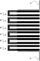
図28は、本実施の形態のフィルタの、導体線路部分のパターンを示す平面図である。ここでは、図8に示した共振器と同様の形状の共振器を、共振器60、62、64、66、68、70として6個直列に配置し、6段のチェビシェフ型フィルタを構成している。共振器群の両側には、L字型の導体線路が共振器に近接して配置され、基板端部まで延伸されて入出力フィーダ72、74となっている。
FIG. 28 is a plan view showing a pattern of a conductor line portion of the filter according to the present embodiment. Here, six resonators having the same shape as the resonator shown in FIG. 8 are arranged in series as resonators 60, 62, 64, 66, 68, and 70 to form a six-stage Chebyshev filter. Yes. On both sides of the resonator group, L-shaped conductor lines are arranged close to the resonator, and are extended to the end of the substrate to form input /
このように、低損失かつ高耐電力の共振器を用いて構成することにより、低損失かつ高耐電力のフィルタを実現できる。なお、ここでは、6段のチェビシェフ型フィルタを例に説明したが、これに限らず、単数もしくは複数の共振器を用いて構成することで、帯域通過型、帯域阻止型、高域通過型、低域通過型等の様々なタイプのフィルタに本発明を適用することが可能となる。 Thus, a low loss and high power durability filter can be realized by using a low loss and high power durability resonator. Here, the six-stage Chebyshev type filter has been described as an example. However, the present invention is not limited to this, and by using one or a plurality of resonators, a band-pass type, a band-stop type, a high-pass type, The present invention can be applied to various types of filters such as a low-pass type.
以上、具体例を参照しつつ本発明の実施の形態について説明した。実施の形態の説明においては、共振器、フィルタ等で、本発明の説明に直接必要としない部分等については記載を省略したが、必要とされる共振器、フィルタ等に関わる要素を適宜選択して用いることができる。 The embodiments of the present invention have been described above with reference to specific examples. In the description of the embodiments, the description of the resonators, filters, etc. that are not directly required for the description of the present invention is omitted, but the elements related to the required resonators, filters, etc. are appropriately selected. Can be used.
その他、本発明の要素を具備し、当業者が適宜設計変更しうる全ての共振器およびフィルタは、本発明の範囲に包含される。本発明の範囲は、特許請求の範囲およびその均等物の範囲によって定義されるものである。 In addition, all resonators and filters that include elements of the present invention and can be appropriately modified by those skilled in the art are included in the scope of the present invention. The scope of the present invention is defined by the appended claims and equivalents thereof.
10 導体線路
12、14 縁端部
20、22、24、26、28 スリット
40、44 誘電体基板
42、46 接地板
60、62、64、66、68、70 共振器
72、74 入出力フィーダ
DESCRIPTION OF
Claims (7)
前記伝送線路がストリップライン構造またはマイクロストリップライン構造を有し、
前記導体線路の前記曲がり部に、前記導体線路の伸長方向に沿った複数本のスリットが設けられ、
前記スリット間にある線路の線幅が、前記曲がり部の外側から内側に向かうに従って細くなっていることを特徴とする共振器。 A resonator composed of a transmission line including a conductor line having a bent portion,
The transmission line has a stripline structure or a microstripline structure;
A plurality of slits along the extending direction of the conductor line are provided in the bent portion of the conductor line,
The resonator, wherein the line width between the slits becomes narrower from the outside to the inside of the bent portion.
A filter comprising the resonator according to any one of claims 1 to 6.
Priority Applications (3)
| Application Number | Priority Date | Filing Date | Title |
|---|---|---|---|
| JP2007304571A JP4489113B2 (en) | 2007-11-26 | 2007-11-26 | Resonator and filter |
| US12/323,255 US7983728B2 (en) | 2007-11-26 | 2008-11-25 | Resonator comprised of a bent conductor line with slits therein and a filter formed therefrom |
| EP08253812.5A EP2065965B1 (en) | 2007-11-26 | 2008-11-26 | Resonator and filter |
Applications Claiming Priority (1)
| Application Number | Priority Date | Filing Date | Title |
|---|---|---|---|
| JP2007304571A JP4489113B2 (en) | 2007-11-26 | 2007-11-26 | Resonator and filter |
Publications (2)
| Publication Number | Publication Date |
|---|---|
| JP2009130699A JP2009130699A (en) | 2009-06-11 |
| JP4489113B2 true JP4489113B2 (en) | 2010-06-23 |
Family
ID=40456255
Family Applications (1)
| Application Number | Title | Priority Date | Filing Date |
|---|---|---|---|
| JP2007304571A Active JP4489113B2 (en) | 2007-11-26 | 2007-11-26 | Resonator and filter |
Country Status (3)
| Country | Link |
|---|---|
| US (1) | US7983728B2 (en) |
| EP (1) | EP2065965B1 (en) |
| JP (1) | JP4489113B2 (en) |
Families Citing this family (11)
| Publication number | Priority date | Publication date | Assignee | Title |
|---|---|---|---|---|
| JP5419088B2 (en) * | 2010-01-07 | 2014-02-19 | アルパイン株式会社 | Substrate attenuation circuit |
| WO2011111120A1 (en) * | 2010-03-12 | 2011-09-15 | 株式会社 東芝 | Communication device |
| FR2977382A1 (en) * | 2011-06-29 | 2013-01-04 | Thomson Licensing | HIGH REJECTION BAND STOP FILTER AND DUPLEXER USING SUCH FILTERS |
| US20130328645A1 (en) * | 2012-06-08 | 2013-12-12 | International Business Machines Corporation | Plating Stub Resonance Shift with Filter Stub Design Methodology |
| JP5780524B2 (en) * | 2012-08-07 | 2015-09-16 | 国立大学法人山梨大学 | Double strip resonator |
| JP6265460B2 (en) * | 2013-06-01 | 2018-01-24 | 国立大学法人山梨大学 | Dual band resonator and dual band bandpass filter using the same |
| JP6265461B2 (en) * | 2013-07-04 | 2018-01-24 | 国立大学法人山梨大学 | Resonator-loaded dual-band resonator and dual-band filter using the same |
| WO2015015959A1 (en) * | 2013-08-02 | 2015-02-05 | 株式会社村田製作所 | High-frequency signal transmission line and electronic device |
| JP6265478B2 (en) * | 2014-01-29 | 2018-01-24 | 国立大学法人山梨大学 | Tunable dual-band bandpass filter |
| JP6236701B2 (en) * | 2014-12-09 | 2017-11-29 | 国立大学法人山梨大学 | Improved tunable dual-band bandpass filter |
| JP6913505B2 (en) | 2017-05-01 | 2021-08-04 | 東京計器株式会社 | Dual band resonator and dual band passband filter using it |
Family Cites Families (8)
| Publication number | Priority date | Publication date | Assignee | Title |
|---|---|---|---|---|
| JP3587264B2 (en) | 1993-09-22 | 2004-11-10 | 株式会社村田製作所 | Stripline and transmission line, resonator and filter using it |
| CA2148341C (en) | 1995-05-01 | 1997-02-04 | Shen Ye | Method and structure for high power hts transmission lines using strips separated by a gap |
| JP2894245B2 (en) | 1995-05-26 | 1999-05-24 | 株式会社移動体通信先端技術研究所 | High frequency transmission line |
| US5909087A (en) | 1996-03-13 | 1999-06-01 | Lutron Electronics Co. Inc. | Lighting control with wireless remote control and programmability |
| US5888942A (en) * | 1996-06-17 | 1999-03-30 | Superconductor Technologies, Inc. | Tunable microwave hairpin-comb superconductive filters for narrow-band applications |
| JPH11177310A (en) | 1997-10-09 | 1999-07-02 | Murata Mfg Co Ltd | High frequency transmission line, dielectric resonator, filter, duplexer and communication equipment |
| JP3391271B2 (en) * | 1998-09-01 | 2003-03-31 | 株式会社村田製作所 | Low loss electrode for high frequency |
| JP4822970B2 (en) | 2006-07-27 | 2011-11-24 | 富士通株式会社 | Split microstrip line resonator and filter using the same |
-
2007
- 2007-11-26 JP JP2007304571A patent/JP4489113B2/en active Active
-
2008
- 2008-11-25 US US12/323,255 patent/US7983728B2/en active Active
- 2008-11-26 EP EP08253812.5A patent/EP2065965B1/en active Active
Also Published As
| Publication number | Publication date |
|---|---|
| US20090146762A1 (en) | 2009-06-11 |
| EP2065965B1 (en) | 2013-06-19 |
| US7983728B2 (en) | 2011-07-19 |
| JP2009130699A (en) | 2009-06-11 |
| EP2065965A1 (en) | 2009-06-03 |
Similar Documents
| Publication | Publication Date | Title |
|---|---|---|
| JP4489113B2 (en) | Resonator and filter | |
| KR100892024B1 (en) | Bandpass filter | |
| US11063330B2 (en) | Filter | |
| US10128552B2 (en) | Structure and electronic circuit | |
| JP2007306290A (en) | Transmission line | |
| US20160365616A1 (en) | Ground structures between resonators for distributed electromagnetic wave filters | |
| JP6341341B2 (en) | Coupling window of dielectric waveguide resonator and dielectric waveguide filter using the same | |
| KR101154091B1 (en) | Meta-material mimo antenna | |
| US20070056764A1 (en) | Transmission line apparatus | |
| JP6265478B2 (en) | Tunable dual-band bandpass filter | |
| JP4411315B2 (en) | Band stop filter | |
| JP2014036258A (en) | Multiband band-pass filter | |
| JP4230467B2 (en) | High frequency filter using coplanar line type resonator. | |
| US11211678B2 (en) | Dual-band resonator and dual-band bandpass filter using same | |
| JP5780524B2 (en) | Double strip resonator | |
| Vincent et al. | Meandered line microstrip filter with suppression of harmonic passband response | |
| JP6151071B2 (en) | Filters and resonators | |
| JP5674494B2 (en) | High frequency filter and high frequency module | |
| JP2004349966A (en) | Superconductive filter | |
| JP2008042608A (en) | Band pass filter | |
| KR100571135B1 (en) | Compact and high performance lowpass filter using complementarily combined characteristics of slot and open stub | |
| JP2010081520A (en) | Structure of radio wave radiator with reflection layer | |
| CN107834136B (en) | Band-pass filter | |
| KR100698315B1 (en) | Transmission line | |
| JP2007166270A (en) | Short-circuiting means, and tip short-circuiting stub therewith, resonator and high-frequency filter |
Legal Events
| Date | Code | Title | Description |
|---|---|---|---|
| A131 | Notification of reasons for refusal |
Free format text: JAPANESE INTERMEDIATE CODE: A131 Effective date: 20091208 |
|
| A521 | Written amendment |
Free format text: JAPANESE INTERMEDIATE CODE: A523 Effective date: 20100203 |
|
| TRDD | Decision of grant or rejection written | ||
| A01 | Written decision to grant a patent or to grant a registration (utility model) |
Free format text: JAPANESE INTERMEDIATE CODE: A01 Effective date: 20100302 |
|
| A01 | Written decision to grant a patent or to grant a registration (utility model) |
Free format text: JAPANESE INTERMEDIATE CODE: A01 |
|
| A61 | First payment of annual fees (during grant procedure) |
Free format text: JAPANESE INTERMEDIATE CODE: A61 Effective date: 20100330 |
|
| FPAY | Renewal fee payment (event date is renewal date of database) |
Free format text: PAYMENT UNTIL: 20130409 Year of fee payment: 3 |
|
| R151 | Written notification of patent or utility model registration |
Ref document number: 4489113 Country of ref document: JP Free format text: JAPANESE INTERMEDIATE CODE: R151 |
|
| FPAY | Renewal fee payment (event date is renewal date of database) |
Free format text: PAYMENT UNTIL: 20130409 Year of fee payment: 3 |
|
| FPAY | Renewal fee payment (event date is renewal date of database) |
Free format text: PAYMENT UNTIL: 20140409 Year of fee payment: 4 |