JP4479823B2 - Semiconductor device - Google Patents
Semiconductor device Download PDFInfo
- Publication number
- JP4479823B2 JP4479823B2 JP2008112483A JP2008112483A JP4479823B2 JP 4479823 B2 JP4479823 B2 JP 4479823B2 JP 2008112483 A JP2008112483 A JP 2008112483A JP 2008112483 A JP2008112483 A JP 2008112483A JP 4479823 B2 JP4479823 B2 JP 4479823B2
- Authority
- JP
- Japan
- Prior art keywords
- reference circuit
- potential
- potential reference
- circuit portion
- semiconductor device
- Prior art date
- Legal status (The legal status is an assumption and is not a legal conclusion. Google has not performed a legal analysis and makes no representation as to the accuracy of the status listed.)
- Expired - Fee Related
Links
Images


Classifications
-
- H—ELECTRICITY
- H01—ELECTRIC ELEMENTS
- H01L—SEMICONDUCTOR DEVICES NOT COVERED BY CLASS H10
- H01L2224/00—Indexing scheme for arrangements for connecting or disconnecting semiconductor or solid-state bodies and methods related thereto as covered by H01L24/00
- H01L2224/01—Means for bonding being attached to, or being formed on, the surface to be connected, e.g. chip-to-package, die-attach, "first-level" interconnects; Manufacturing methods related thereto
- H01L2224/42—Wire connectors; Manufacturing methods related thereto
- H01L2224/47—Structure, shape, material or disposition of the wire connectors after the connecting process
- H01L2224/48—Structure, shape, material or disposition of the wire connectors after the connecting process of an individual wire connector
- H01L2224/481—Disposition
- H01L2224/48151—Connecting between a semiconductor or solid-state body and an item not being a semiconductor or solid-state body, e.g. chip-to-substrate, chip-to-passive
- H01L2224/48221—Connecting between a semiconductor or solid-state body and an item not being a semiconductor or solid-state body, e.g. chip-to-substrate, chip-to-passive the body and the item being stacked
- H01L2224/48245—Connecting between a semiconductor or solid-state body and an item not being a semiconductor or solid-state body, e.g. chip-to-substrate, chip-to-passive the body and the item being stacked the item being metallic
- H01L2224/48247—Connecting between a semiconductor or solid-state body and an item not being a semiconductor or solid-state body, e.g. chip-to-substrate, chip-to-passive the body and the item being stacked the item being metallic connecting the wire to a bond pad of the item
-
- H—ELECTRICITY
- H01—ELECTRIC ELEMENTS
- H01L—SEMICONDUCTOR DEVICES NOT COVERED BY CLASS H10
- H01L2924/00—Indexing scheme for arrangements or methods for connecting or disconnecting semiconductor or solid-state bodies as covered by H01L24/00
- H01L2924/10—Details of semiconductor or other solid state devices to be connected
- H01L2924/11—Device type
- H01L2924/13—Discrete devices, e.g. 3 terminal devices
- H01L2924/1304—Transistor
- H01L2924/1305—Bipolar Junction Transistor [BJT]
- H01L2924/13055—Insulated gate bipolar transistor [IGBT]
-
- H—ELECTRICITY
- H01—ELECTRIC ELEMENTS
- H01L—SEMICONDUCTOR DEVICES NOT COVERED BY CLASS H10
- H01L2924/00—Indexing scheme for arrangements or methods for connecting or disconnecting semiconductor or solid-state bodies as covered by H01L24/00
- H01L2924/10—Details of semiconductor or other solid state devices to be connected
- H01L2924/11—Device type
- H01L2924/13—Discrete devices, e.g. 3 terminal devices
- H01L2924/1304—Transistor
- H01L2924/1306—Field-effect transistor [FET]
- H01L2924/13091—Metal-Oxide-Semiconductor Field-Effect Transistor [MOSFET]
Description
本発明は、モータ等の機器を駆動させるためのインバータ制御用の素子等に用いられる半導体装置に関するものである。 The present invention relates to a semiconductor device used for an inverter control element or the like for driving a device such as a motor.
モータ等の負荷を駆動させるためのインバータ制御用の素子等に用いられる半導体装置として、HVIC(High Voltage Integrated Circuit)がある。このHVICにより、負荷を駆動するためのインバータ内に備えられるパワーデバイスを制御する。 As a semiconductor device used for an inverter control element or the like for driving a load such as a motor, there is an HVIC (High Voltage Integrated Circuit). The HVIC controls the power device provided in the inverter for driving the load.
従来、インバータの駆動には、図10に示すように、モータ100の駆動を行うインバータ回路101のハイサイド側のIGBT102aを駆動する高電圧基準回路に相当する高電圧基準ゲート駆動回路103とローサイド側のIGBT102bを駆動する低電圧基準回路に相当する低電位基準ゲート駆動回路104を備えると共に、これらの間にレベルシフト素子105a、105bおよび制御回路106が備えられたHVIC107が用いられている。このHVIC107では、レベルシフト素子105a、105bを通じて信号伝達を行うことにより高電位基準回路と低電圧基準回路における基準電圧のレベルシフトを行っている。このようなHVIC107では、インバータの小型化の為に、1チップ化(HVIC化)が進められており、図10に示したHVIC107も1チップにて構成されている。
Conventionally, as shown in FIG. 10, the inverter is driven by a high-voltage reference
しかしながら、このように1チップ化したHVIC107では、高電位基準回路と低電位基準回路との間で電位の干渉が発生し、回路を誤動作させるという問題があった。このため、従来では、JI分離構造、誘電体分離構造、SOI(Silicon on insulator)基板を用いたトレンチ分離構造(例えば、特許文献1参照)などにより素子分離を行っている。ところが、高電位基準回路のIGBT102aを駆動するための出力部の電位を高電圧側の基準とするための仮想GND電位にする必要があるため、上記したいずれの素子分離構造においてもレベルシフトにおける低電位(例えば0V)から高電位(例えば750V)に切り替えるときに高電圧(例えば1200Vを超える電圧)が数十kV/μsecという早い立ち上がり速度で生じ、大きな電位振幅が生じる。この立ち上がりの早い高電圧サージ(以下、立ち上がり時間に対する電圧上昇が高いことからdv/dtサージという)を回路の誤動作無く扱うことは難しい。
上記した素子分離構造の中では、SOI基板を用いたトレンチ分離構造が最もノイズに強く、素子分離としては最もポテンシャルが高いと考えられる。しかしながら、この構造を用いて高耐圧のレベルシフト素子を開発してきたところ、SOI基板を用いたトレンチ分離構造のHVICにおいても、dv/dtサージが印加された際に支持基板を介して電位が干渉し、支持基板と活性層(SOI層)との間に配置された埋込酸化膜(BOX:Buried Oxide)にて形成される寄生容量を充放電する変位電流が発生し、回路を誤動作させてしまうという問題が生じた。図11は、変位電流が発生する様子を示したHVICの断面図である。この図に示すように、例えば、SOI層111に形成された高電位基準回路部HVの仮想GND電位とされる部位からBOXにて構成される埋込層113を介して支持基板112に流れたのち、再び埋込層113を介して低電位基準回路部LVのGND電位とされる部位に流れ込むという経路で変位電流が発生する。
Among the element isolation structures described above, the trench isolation structure using an SOI substrate is considered to be the most resistant to noise and has the highest potential for element isolation. However, when a level shift element having a high withstand voltage has been developed using this structure, even in an HVIC having a trench isolation structure using an SOI substrate, the potential interferes with the support substrate when a dv / dt surge is applied. In addition, a displacement current that charges and discharges a parasitic capacitance formed by a buried oxide film (BOX) disposed between the support substrate and the active layer (SOI layer) is generated, causing the circuit to malfunction. The problem of end. FIG. 11 is a cross-sectional view of the HVIC showing how the displacement current is generated. As shown in this figure, for example, the high potential reference circuit unit HV formed in the
このような問題は、BOX膜厚を厚くして寄生容量を低減したり、支持基板112側の不純物濃度を下げて高抵抗にして変位電流の伝搬を低減することで抑制可能であるが、高増幅率のアンプ回路等を集積する場合には僅かな変位電流でも誤動作の要因となり、完全な対策は難しい。
Such a problem can be suppressed by reducing the parasitic capacitance by increasing the BOX film thickness, or by reducing the impurity concentration on the
本発明は上記点に鑑みて、トレンチ分離構造により低電位基準回路と高電位基準回路およびレベルシフト素子を備えた半導体装置を構成する場合において、dv/dtサージにより、寄生容量を充放電する変位電流が発生することを抑制し、回路の誤動作を防止することを目的とする。 In view of the above points, the present invention provides a displacement for charging / discharging parasitic capacitance by a dv / dt surge when a semiconductor device including a low potential reference circuit, a high potential reference circuit, and a level shift element is formed by a trench isolation structure. An object of the present invention is to suppress the occurrence of current and prevent malfunction of the circuit.
上記目的を達成するため、請求項1に記載の発明では、半導体層(1)の裏面のうち少なくとも低電位基準回路部(LV)と対応する部分および高電位基準回路部(HV)と対応する部分に絶縁部材(2、50、60、70)を配置し、絶縁部材(2、50、60、70)を挟んで低電位基準回路部(LV)と対向するように、低電位基準回路部(LV)における第1の電位が印加される部位と電気的に接続された第1導体部材(3a、40a)を配置すると共に、絶縁部材(2、50、60、70)を挟んで高電位基準回路部(HV)と対向するように、高電位基準回路部(HV)における第2の電位が印加される部位と電気的に接続される第2導体部材(3b、40b)を配置することを特徴としている。 In order to achieve the above object, according to the first aspect of the present invention, at least the portion corresponding to the low potential reference circuit portion (LV) and the high potential reference circuit portion (HV) on the back surface of the semiconductor layer (1). The insulating member (2, 50, 60, 70) is disposed in the portion, and the low potential reference circuit unit is opposed to the low potential reference circuit unit (LV) with the insulating member (2, 50, 60, 70) interposed therebetween. The first conductor member (3a, 40a) electrically connected to the portion to which the first potential in (LV) is applied is disposed, and the high potential with the insulating member (2, 50, 60, 70) interposed therebetween Arranging the second conductor members (3b, 40b) electrically connected to the portion to which the second potential is applied in the high potential reference circuit portion (HV) so as to face the reference circuit portion (HV). It is characterized by.
このように構成された半導体装置では、低電位基準回路部(LV)と対応するように第1導体部材(3a、40a)が配置されていると共に、高電位基準回路部(HV)と対応するように第2導体部材(3b、40b)が配置された構造とされている。このため、絶縁部材(2、50、60、70)のうち低電位基準回路部(LV)の下方に位置する部分は、低電位基準回路部(LV)と第1導体部材(3a、40a)とがほぼ同電位となることで、同電位に挟まれた状態となる。同様に、絶縁基板2のうち高電位基準回路部(HV)の下方に位置する部分は、高電位基準回路部(HV)と第2導体部材(3b、40b)とがほぼ同電位となることで、同電位に挟まれた状態となる。
In the semiconductor device configured as described above, the first conductor members (3a, 40a) are disposed so as to correspond to the low potential reference circuit portion (LV) and also correspond to the high potential reference circuit portion (HV). Thus, the second conductor member (3b, 40b) is arranged. Therefore, portions of the insulating members (2, 50, 60, 70) located below the low potential reference circuit portion (LV) are the low potential reference circuit portion (LV) and the first conductor members (3a, 40a). And become substantially the same potential, so that they are sandwiched between the same potential. Similarly, in the portion of the
したがって、半導体装置内に形成される寄生容量両端の電位差を無くすことが可能となり、容量値をキャンセルできる。これにより、dv/dtサージによって寄生容量を充放電する変位電流が発生することを防止することができ、回路の誤動作を防止することが可能となる。 Therefore, it is possible to eliminate the potential difference between both ends of the parasitic capacitance formed in the semiconductor device, and the capacitance value can be canceled. Thereby, it is possible to prevent a displacement current that charges and discharges the parasitic capacitance due to the dv / dt surge, and to prevent malfunction of the circuit.
例えば、請求項2に記載したように、低電位基準回路部(LV)における第1の電位が印加される部位と第1導体部材(3a、40a)との電気的接続、および、高電位基準回路部(HV)における第2の電位が印加される部位と第2導体部材(3b、40b)との電気的接続をボンディングワイヤ(4)にて行うことができる。
For example, as described in
また、請求項3に記載したように、絶縁部材(2、50、60、70)のうち、低電位基準回路部(LV)と対応する部分および高電位基準回路部(HV)と対応する部分にトレンチ(31)を埋め込むように貫通電極(30)を備えておき、該貫通電極(30)にて、低電位基準回路部(LV)における第1の電位が印加される部位と第1導体部材(3a、40a)との電気的接続、および、高電位基準回路部(HV)における第2の電位が印加される部位と第2導体部材(3b、40b)との電気的接続を行うこともできる。
Further, as defined in
また、請求項4に記載したように、第1、第2導体部材に関しては、低電位基準回路部(LV)および高電位基準回路部(HV)を外部と電気的に接続するためのリードフレーム(3)となる第1、第2リードフレーム(3a、3b)により構成することができる。 According to a fourth aspect of the present invention, the lead frame for electrically connecting the low potential reference circuit portion (LV) and the high potential reference circuit portion (HV) to the outside with respect to the first and second conductor members. It can be constituted by the first and second lead frames (3a, 3b) to be (3).
同様に、請求項5に記載したように、第1、第2導体部材を基板(41)上にパターン形成された第1、第2導体パターン(40a、40b)にて構成することもできる。 Similarly, as described in claim 5, the first and second conductor members can be constituted by the first and second conductor patterns (40a, 40b) patterned on the substrate (41).
この場合、請求項6に記載したように、半導体層(1)を封止する封止樹脂(60)にて絶縁部材を構成することもできる。さらに、この場合、請求項7に記載したように、封止樹脂(60)内に一端が配置され、他端が封止樹脂(60)から外に露出させられた複数のリードフレーム(61)を備え、該複数のリードフレーム(61)の一端が低電位基準回路部(LV)における第1の電位が印加される部位および高電位基準回路部(HV)における第2の電位が印加される部位と電気的に接続され、リードフレーム(61)の他端が第1、第2導体パターン(40a、40b)に接続されるような構造とすることができる。 In this case, as described in the sixth aspect, the insulating member can also be constituted by the sealing resin (60) for sealing the semiconductor layer (1). Further, in this case, as described in claim 7, a plurality of lead frames (61) having one end disposed in the sealing resin (60) and the other end exposed to the outside from the sealing resin (60). One end of the plurality of lead frames (61) to which the first potential in the low potential reference circuit portion (LV) is applied and the second potential in the high potential reference circuit portion (HV) is applied. The lead frame (61) may be electrically connected to the portion and the other end of the lead frame (61) may be connected to the first and second conductor patterns (40a, 40b).
また、請求項8に記載したように、半導体層(1)がマウントされるセラミックパッケージ(70)にて絶縁部材を構成することもできる。この場合、請求項9に記載したように、セラミックパッケージ(70)のうち半導体層(1)がマウントされる部分に形成された凹部(70a)から一端が露出させられると共に、他端もセラミックパッケージ(70)から外に露出させられた複数のリードフレーム(61)を備え、該複数のリードフレーム(61)の一端が低電位基準回路部(LV)における第1の電位が印加される部位および高電位基準回路部(HV)における第2の電位が印加される部位と電気的に接続され、リードフレーム(61)の他端が第1、第2導体パターン(40a、40b)に接続されるような構造とすることができる。
In addition, as described in
勿論、請求項10に記載したように、絶縁部材を絶縁基板(2)または絶縁膜(50)にて構成することもできる。 Of course, as described in the tenth aspect, the insulating member may be formed of an insulating substrate (2) or an insulating film (50).
なお、上記各手段の括弧内の符号は、後述する実施形態に記載の具体的手段との対応関係を示すものである。 In addition, the code | symbol in the bracket | parenthesis of each said means shows the correspondence with the specific means as described in embodiment mentioned later.
以下、本発明の実施形態について図に基づいて説明する。なお、以下の各実施形態相互において、互いに同一もしくは均等である部分には、図中、同一符号を付してある。 Hereinafter, embodiments of the present invention will be described with reference to the drawings. In the following embodiments, the same or equivalent parts are denoted by the same reference numerals in the drawings.
(第1実施形態)
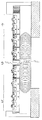
本発明の第1実施形態について説明する。図1は、本実施形態にかかる半導体装置(HVIC)の断面図である。また、図2は、図1に示す半導体装置を上面側から見た時のレイアウト図である。なお、図1は、本図のA−A断面図に相当する図である。
(First embodiment)
A first embodiment of the present invention will be described. FIG. 1 is a cross-sectional view of a semiconductor device (HVIC) according to the present embodiment. FIG. 2 is a layout diagram when the semiconductor device shown in FIG. 1 is viewed from the upper surface side. FIG. 1 is a diagram corresponding to a cross-sectional view taken along the line AA in FIG.
以下、これらの図を参照して、本実施形態の半導体装置の構成について説明する。なお、以下の説明では、図1の紙面上方を半導体装置の表面側、紙面下方を半導体装置の裏面側として説明する。 Hereinafter, the configuration of the semiconductor device of this embodiment will be described with reference to these drawings. In the following description, the upper side in FIG. 1 is described as the front side of the semiconductor device, and the lower side in FIG. 1 is described as the back side of the semiconductor device.
図1に示すように、本実施形態の半導体装置は、例えばn型シリコンにて構成された半導体層1が絶縁基板2を介してリードフレーム3に接合され、半導体層1内の所望位置がボンディングワイヤ4を通じてリードフレーム3に電気的に接続されることで構成されている。
As shown in FIG. 1, in the semiconductor device of this embodiment, a
半導体層1は、半導体装置の表面側に配置され、シリコン基板を所定膜厚に研削することにより構成されている。この半導体層1は、複数のトレンチ分離部5により素子分離されている。各トレンチ分離部5は、半導体層1の表面から絶縁基板2に達するトレンチ6とトレンチ6内に配置された絶縁膜7によって構成されており、例えば同等幅にて構成されている。
The
複数のトレンチ分離部5は多重リング構造とされており、最も外側とそれよりも1つ内側のトレンチ分離部5の間に形成される領域(つまり図1、図2の紙面左側の領域)が低電位基準回路部LV、最も内側のトレンチ分離部5内の領域(つまり紙面右側の領域)が高電位基準回路部HV、これら低電位基準回路部LVと高電位基準回路部HVの間に形成される領域がレベルシフト素子形成部LSとされている。 The plurality of trench isolation portions 5 have a multi-ring structure, and a region formed between the outermost trench isolation portion 5 and the innermost trench isolation portion 5 (that is, the region on the left side in FIG. 1 and FIG. 2). The low potential reference circuit portion LV, and the region in the innermost trench isolation portion 5 (that is, the region on the right side of the drawing) is formed between the high potential reference circuit portion HV and the low potential reference circuit portion LV and the high potential reference circuit portion HV. The region to be formed is a level shift element forming portion LS.
半導体層1における低電位基準回路部LVには、小電位にて駆動されるロジック回路などの信号処理回路が構成されており、これらは0V(第1の電位)を基準電位として動作する。低電位基準回路部LVは、トレンチ分離部5にて半導体装置の他の部分から素子分離されている。この低電位基準回路部LVには、CMOS10などのように信号処理回路を構成する各種素子が備えられている。具体的には、半導体層1内がSTI(Shallow Trench Isolation)やLOCOS酸化膜等の素子分離用の絶縁膜11にて素子分離されており、素子分離された各領域はnウェル層12aもしくはpウェル層12bとされている。nウェル層12a内にはp+型ソース領域13aおよびp+型ドレイン領域14aが構成され、pウェル層12b内にはn+型ソース領域13bおよびn+型ドレイン領域14bが構成されている。そして、p+型ソース領域13aとp+型ドレイン領域14aの間に位置するnウェル層12aの表面、および、n+型ソース領域13bおよびn+型ドレイン領域14bの間に位置するpウェル層12bの表面に、ゲート絶縁膜15a、15bを介してゲート電極16a、16bが形成されている。これにより、nチャネルMOSFETとpチャネルMOSFETにて構成されたCMOS10が構成されている。
The low potential reference circuit portion LV in the
なお、半導体層1の表面側には、CMOS10を構成するゲート電極16a、16bや各ソース領域13a、13bもしくは各ドレイン領域14a、14bと電気的に接続される配線部や層間絶縁膜などが形成されているが、ここでは図示を省略してある。また、CMOS10の他にも、バイポーラトランジスタや拡散抵抗、さらにはメモリなども備えられるが、これらの構造は周知であるため、ここでは代表してCMOS10のみを示してある。
On the surface side of the
半導体層1における高電位基準回路部HVには、高電位にて駆動されるロジック回路などの信号処理回路が構成されている。これらは低電位基準回路部LVの基準電位よりも高い電位(第2の電位)、例えば1200Vを基準電位として動作する。高電位基準回路部HVは、トレンチ分離部5にて半導体装置の他の部分から素子分離されている。この高電位基準回路部HVにも、低電位基準回路部LVと同様の構造のCMOS10が備えられており、図示しないがバイポーラトランジスタや拡散抵抗、さらにはメモリなども備えられている。
The high potential reference circuit portion HV in the
また、半導体層1におけるレベルシフト素子形成部LSには、レベルシフト素子として高耐圧LDMOS20が形成されている。高耐圧LDMOS20は、半導体層1の表層にそれぞれ位置するn型ドレイン領域21、p型チャネル領域22、n+型ソース領域23を有している。n型ドレイン領域21の表層にはn+型コンタクト層24が形成されており、p型チャネル領域22の表層にはp+型コンタクト層25が形成されている。また、n型ドレイン領域21とp型チャネル領域22は、いわゆるLOCOS酸化膜26により、分離されている。そして、p型チャネル領域22上には、ゲート絶縁膜27を介して、ゲート電極28が配置されている。これにより、高耐圧LDMOS20が構成されている。
In the level shift element forming portion LS in the
なお、半導体層1の表面側には、ゲート電極28、n+型ソース領域23およびp+型コンタクト層25、もしくは、n+型コンタクト層24と電気的に接続される配線部や層間絶縁膜が形成されているが、ここでは図示を省略してある。
Note that, on the surface side of the
このような構造の高耐圧LDMOS20は複数セル形成されており、低電位基準回路部LVと高電位基準回路部HVとの間において複数セルが配置されると共に、各セルがトレンチ分離部5によって素子分離されている。
The high
一方、絶縁基板2は、ガラス基板や樹脂等の絶縁材料で構成されており、本発明でいう絶縁部材を構成している。絶縁基板2の厚みは任意であるが、後述するように、半導体装置の作動時に絶縁基板2内での電位の偏りが発生するため、半導体層1とリードフレームとの絶縁を確保できる程度の厚みを確保しつつ、より薄くするのが好ましい。すなわち、絶縁基板2の構成材料、具体的には絶縁基板2の誘電率によって電位の偏りが変わるため、絶縁基板2の構成材料により絶縁基板2の好ましい厚みが適宜決まることになる。
On the other hand, the insulating
また、リードフレーム3は、本発明における導体部材を構成するものであり、本実施形態では、低電位基準回路部LVの基準電位の印加や高電位基準回路部HVの基準電位の印加のために用いられている。
The
リードフレーム3は、図1および図2に示されるように、低電位基準回路部LV側と対応する部分の下方と高電位基準回路部HV側と対応する部分の下方それぞれに対向するように配置されている。そして、図1に示すように、低電位基準回路部LV側と対応する第1リードフレーム3aは、低電位基準回路部LVとレベルシフト素子形成部LSとを分離するトレンチ分離部5よりもレベルシフト素子形成部LS側まで距離L1入り込むように設計されている。また、高電位基準回路部HV側と対応する第2リードフレーム3bも、高電位基準回路部HVとレベルシフト素子形成部LSとを分離するトレンチ分離部5よりもレベルシフト素子形成部LS側まで距離L2入り込むように設計されている。
As shown in FIGS. 1 and 2, the
距離L1、L2は、半導体装置製造時の位置ズレを考慮したものであり、基本的には距離L1=距離L2として設計されている。すなわち、半導体層1に各素子を作り込んだ後、絶縁基板2およびリードフレーム3を位置合わせ貼り合せることになるが、そのときに位置ズレが生じ得る。この位置ズレの最大値を見込んで、位置ズレの最大値分を距離L1=距離L2としている。このため、半導体装置を製造した時に上記位置ズレが生じると、第1、第2リードフレーム3a、3bは同方向にずれるため距離L1≠距離L2となるが、位置ズレの最大値で距離L1、L2を設計しているため、少なくとも第1、第2リードフレーム3a、3bのレベルシフト素子形成部LS側の端部が低電位基準回路部LVもしくは高電位基準回路部HVとレベルシフト素子形成部LSとを分離するトレンチ分離部5よりも外側に位置しないようにできる。
The distances L1 and L2 take into account the positional deviation at the time of manufacturing the semiconductor device, and are basically designed such that the distance L1 = the distance L2. That is, after each element is formed in the
そして、第1リードフレーム3aは、ボンディングワイヤ4を通じて低電位基準回路部LV内の基準電位を印加するライン(図示せず)に電気的に接続され、第2リードフレーム3bは、ボンディングワイヤ4を通じて高電位基準回路部HV内の基準電位を印加するライン(図示せず)に電気的に接続されている。
The
このように構成された半導体装置では、低電位基準回路部LVと対応するように第1リードフレーム3aが配置されていると共に、高電位基準回路部HVと対応するように第2リードフレーム3bが配置された構造とされている。このため、絶縁基板2のうち低電位基準回路部LVの下方に位置する部分は、低電位基準回路部LVと第1リードフレーム3aとがほぼ同電位となることで、同電位に挟まれた状態となる。同様に、絶縁基板2のうち高電位基準回路部HVの下方に位置する部分は、高電位基準回路部HVと第2リードフレーム3bとがほぼ同電位となることで、同電位に挟まれた状態となる。
In the semiconductor device configured as described above, the
したがって、半導体装置内に形成される寄生容量両端の電位差を無くすことが可能となり、容量値をキャンセルできる。これにより、dv/dtサージによって寄生容量を充放電する変位電流が発生することを防止することができ、回路の誤動作を防止することが可能となる。 Therefore, it is possible to eliminate the potential difference between both ends of the parasitic capacitance formed in the semiconductor device, and the capacitance value can be canceled. Thereby, it is possible to prevent a displacement current that charges and discharges the parasitic capacitance due to the dv / dt surge, and to prevent malfunction of the circuit.
なお、このような構造とする場合、絶縁基板2内に高電位基準回路部HV側と低電位基準回路部LV側との間の電位差に基づき、これらの間に電界が発生することになる。図3は、図1に示す半導体装置における絶縁基板2内の等電位分布を示したの模式図である。この図に示されるように、絶縁基板2内の等電位分布は、高電位基準回路部HV側から低電位基準回路部LV側に至る間において、すべてが並行な分布になるのではなく、高電位基準回路部HV側に近づくほど、もしくは低電位基準回路部LV側に近づくほど、電位に偏りが発生する。この電位の偏りにより、あたかも高電位基準回路部HVと電位の偏り部分、および、低電位基準回路部LVと電位の偏り部分との間に寄生容量が形成されたような状態となり、変位電流の要因になる可能性がある。
In the case of such a structure, an electric field is generated in the insulating
このような電位の偏りは、絶縁基板2の誘電率および厚みに依存している。具体的には、電位の偏りは、絶縁基板2の誘電率が高い程または厚みが厚いほど大きくなる。絶縁基板2の誘電率は絶縁基板2の構成材料によって一義的に決まるため、絶縁基板2の構成材料の選択によって決まってしまうが、厚みに関しては適宜設計変更可能なパラメータである。したがって、より変位電流を防止するためには、絶縁基板2の厚みを薄くする方が好ましいと言える。
Such a potential bias depends on the dielectric constant and thickness of the insulating
(第2実施形態)
本発明の第2実施形態について説明する。本実施形態の半導体装置は、第1実施形態に対して低電位基準回路部LV側と第1リードフレーム3aとの電気的接続形態や高電位基準回路部HV側と第2リードフレーム3bの電気的接続形態を変更したものであり、その他に関しては第1実施形態と同様であるため、第1実施形態と異なる部分についてのみ説明する。
(Second Embodiment)
A second embodiment of the present invention will be described. The semiconductor device of the present embodiment is different from the first embodiment in the electrical connection configuration between the low potential reference circuit unit LV side and the
図4は、本実施形態にかかる半導体装置の断面図である。この図に示されるように、絶縁基板2のうち低電位基準回路部LVの下方および高電位基準回路部HVの下方に貫通電極30が備えられている。具体的には、絶縁基板2に対して半導体層1からリードフレーム3に達するようにトレンチ31が形成されており、そのトレンチ31内にアルミニウム等の導体にて構成された貫通電極30が埋め込まれている。
FIG. 4 is a cross-sectional view of the semiconductor device according to the present embodiment. As shown in this figure, through
このように、貫通電極30を通じて、第1リードフレーム3aと低電位基準回路部LV内の基準電位を印加する領域とを電気的に接続し、第2リードフレーム3bと高電位基準回路部HV内の基準電位を印加する領域とを電気的に接続することもできる。このような構成としても、第1実施形態と同様の効果を得ることができる。
Thus, the
(第3実施形態)
本発明の第3実施形態について説明する。本実施形態の半導体装置は、第2実施形態に対してリードフレーム3の代わりに導体パターンを備えた基板を用いたものであり、その他に関しては第1実施形態と同様であるため、第1実施形態と異なる部分についてのみ説明する。
(Third embodiment)
A third embodiment of the present invention will be described. The semiconductor device of the present embodiment uses a substrate provided with a conductor pattern instead of the
図5は、本実施形態にかかる半導体装置の断面図である。この図に示されるように、絶縁基板2の裏面側に、第1、第2実施形態で示したようなリードフレーム3ではなく、導体パターン40を備えた基板41を配置している。本実施形態では、導体パターン40が本発明における導体部材を構成するものであり、低電位基準回路部LVの基準電位の印加や高電位基準回路部HVの基準電位の印加のために用いられている。
FIG. 5 is a cross-sectional view of the semiconductor device according to the present embodiment. As shown in this figure, a
導体パターン40は、図1および図2に示されるように、低電位基準回路部LV側と対応する部分の下方と高電位基準回路部HV側と対応する部分の下方それぞれに配置されている。低電位基準回路部LV側と対応する第1導体パターン40aは、低電位基準回路部LVとレベルシフト素子形成部LSとを分離するトレンチ分離部5よりもレベルシフト素子形成部LS側まで距離L1入り込むように設計されている。また、高電位基準回路部HV側と対応する第2導体パターン40bも、高電位基準回路部HVとレベルシフト素子形成部LSとを分離するトレンチ分離部5よりもレベルシフト素子形成部LS側まで距離L2入り込むように設計されている。
As shown in FIGS. 1 and 2, the
これら距離L1、L2の意味に関しては、第1実施形態のように第1、第2リードフレーム3a、3bを用いる場合と同様であり、導体パターン40および基板41を接合する際に位置ズレが生じても、少なくとも第1、第2導体パターン40a、40bのレベルシフト素子形成部LS側の端部が低電位基準回路部LVもしくは高電位基準回路部HVとレベルシフト素子形成部LSとを分離するトレンチ分離部5よりも外側に位置しないようにできる。
The meanings of these distances L1 and L2 are the same as in the case of using the first and second lead frames 3a and 3b as in the first embodiment, and misalignment occurs when the
そして、第1導体パターン40aは、絶縁基板2の裏面側において貫通電極30に接続されるように配置されたはんだバンプ42を通じて低電位基準回路部LV内の基準電位を印加する領域に電気的に接続され、第2導体パターン40bも、はんだバンプ42を通じて高電位基準回路部HV内の基準電位を印加する領域に電気的に接続されている。
Then, the
このように、リードフレーム3に代えて導体パターン40を用いるような場合であっても、第1実施形態と同様の効果を得ることができる。
Thus, even when the
なお、ここでは第2実施形態のように貫通電極30による電気的接続を行うような構造に対して本実施形態を適用する場合について説明したが、第1実施形態のようにボンディングワイヤ4による電気的接続を行うような構造に対して本実施形態を適用することもできる。すなわち、ボンディングワイヤ4を通じて、第1導体パターン40aと低電位基準回路部LV内の基準電位を印加するラインとを電気的に接続したり、第2導体パターン40bと高電位基準回路部HV内の基準電位を印加するラインとを電気的に接続することもできる。
Here, the case where the present embodiment is applied to a structure in which electrical connection by the through
(第4実施形態)
本発明の第4実施形態について説明する。本実施形態の半導体装置は、第1実施形態に対し、絶縁部材として絶縁基板2の代わりに絶縁膜を用いたものであり、その他に関しては第1実施形態と同様であるため、第1実施形態と異なる部分についてのみ説明する。
(Fourth embodiment)
A fourth embodiment of the present invention will be described. In contrast to the first embodiment, the semiconductor device of the present embodiment uses an insulating film instead of the insulating
図6は、本実施形態にかかる半導体装置の断面図である。この図に示されるように、第1実施形態で用いていた絶縁基板2に代えて、絶縁膜50を用いている。この絶縁膜50は、例えばSOI基板に含まれる埋込酸化膜にて構成されている。すなわち、SOI層と支持基板とが埋込酸化膜を介して貼り合わされたSOI基板のうち、SOI層にて半導体層1を構成すると共に埋込酸化膜にて絶縁膜50を構成し、支持基板に関してはリードフレーム3を貼り合せる前に研削などにより除去した構造とすることで、本実施形態にかかる半導体装置を構成することができる。
FIG. 6 is a cross-sectional view of the semiconductor device according to the present embodiment. As shown in this figure, an insulating
このように、絶縁基板2ではなく、絶縁膜50を用いても、第1実施形態と同様の効果を得ることができる。また、上述したように、絶縁基板2の厚みが薄いほど電位の偏りに起因する変位電流も抑制できることから、絶縁膜50を用いることにより変位電流の抑制が更に可能となり、回路の誤動作を防止することが可能となる。
Thus, even when the insulating
(第5実施形態)
本発明の第5実施形態について説明する。本実施形態の半導体装置は、第3実施形態のように導体パターン40を備えた基板41を用いる場合において、絶縁基板2の代わりに封止樹脂を絶縁部材として用いたものであり、その他に関しては第3実施形態と同様であるため、第3実施形態と異なる部分についてのみ説明する。
(Fifth embodiment)
A fifth embodiment of the present invention will be described. The semiconductor device of this embodiment uses a sealing resin as an insulating member instead of the insulating
図7は、本実施形態にかかる半導体装置の断面図である。この図には示していないが、半導体層1には第3実施形態と同様に低電位基準回路部LVや高電位基準回路部HVおよびレベルシフト素子形成部LSを構成する各種素子が作り込まれており、この半導体層1が封止樹脂60にて封止されている。封止樹脂60内において、低電位基準回路部LV内の基準電位を印加するラインとリードフレーム61の一端とがボンディングワイヤ62を通じて電気的に接続されていると共に、高電位基準回路部HV内基準電位を印加するラインとリードフレーム61の一端とがボンディングワイヤ62を通じて電気的に接続されている。
FIG. 7 is a cross-sectional view of the semiconductor device according to the present embodiment. Although not shown in the drawing, various elements constituting the low potential reference circuit unit LV, the high potential reference circuit unit HV, and the level shift element forming unit LS are formed in the
また、封止樹脂60を挟んで半導体層1の反対側に導体パターン40が形成された基板41が備えられている。そして、封止樹脂60の外部に延設されたリードフレーム61の他端が導体パターン40側に折り曲げられていると共に、導体パターン40に接合されている。これにより、リードフレーム61を介して、第1導体パターン40aと低電位基準回路部LV内の基準電位を印加するラインとが電気的に接続され、第2導体パターン40bと高電位基準回路部HV内の基準電位を印加するラインとが電気的に接続された構造とされている。
In addition, a
このように、封止樹脂60を絶縁部材とする場合においても、封止樹脂60を挟んで半導体層1の反対側に導体パターン40を配置するような構造にすれば、第1実施形態と同様の効果を得ることができる。
As described above, even when the sealing
なお、このような構造は、基板41をプリント基板などの実装基板とし、その表面に第1、第2導体パターン40a、40bとしてパターン配線を備えるような構造としても実現することが可能である。
Such a structure can also be realized as a structure in which the
(第6実施形態)
本発明の第6実施形態について説明する。本実施形態の半導体装置は、第5実施形態の封止樹脂60に代えて、セラミックパッケージを絶縁部材として用いたものであり、その他に関しては第3実施形態と同様であるため、第5実施形態と異なる部分についてのみ説明する。
(Sixth embodiment)
A sixth embodiment of the present invention will be described. The semiconductor device of the present embodiment uses a ceramic package as an insulating member in place of the sealing
図8は、本実施形態にかかる半導体装置の断面図である。この図に示すように、第5実施形態で用いていた封止樹脂60の代わりにセラミックパッケージ70を用いている。セラミックパッケージ70には、表面に凹部70aが形成されており、その凹部70a内に半導体層1がマウントされている。そして、凹部70a内にリードフレーム61の一端が露出させられることで、半導体層1の所望位置とリードフレーム61の一端とがボンディングワイヤ62を介して電気的に接続される構造となっている。
FIG. 8 is a cross-sectional view of the semiconductor device according to the present embodiment. As shown in this figure, a
このように、セラミックパッケージ70を絶縁部材とする場合にも、セラミックパッケージ70を挟んで半導体層1の反対側に導体パターン40を配置するような構造にすることができ、第1実施形態と同様の効果を得ることができる。
Thus, even when the
(他の実施形態)
上記第1〜第4実施形態では、低電位基準回路部LVや高電位基準回路部HVおよびレベルシフト素子形成部LSを構成する素子の一例を記載しているが、これらを構成する素子の種類に関しては適宜変更可能である。また、低電位基準回路部LVや高電位基準回路部HVおよびレベルシフト素子形成部LSのレイアウト等に関しても、適宜変更可能である。
(Other embodiments)
In the first to fourth embodiments, an example of elements constituting the low potential reference circuit unit LV, the high potential reference circuit unit HV, and the level shift element forming unit LS is described. Can be changed as appropriate. Further, the layout of the low potential reference circuit unit LV, the high potential reference circuit unit HV, and the level shift element formation unit LS can be appropriately changed.
また、上記第1〜第3、第5、第6実施形態では、SOI基板を用いない場合、つまりバルク基板やバルク基板にシリコン層をエピタキシャル成長させたエピ基板を用いて半導体層1を構成した場合を例に挙げてについて説明したが、これら各実施形態に関してもSOI基板を用いて構成することもできる。逆に、第4実施形態では、SOI基板を用いる場合について説明したが、バルク基板やエピ基板を用いて半導体層1を形成したのち、半導体層1の裏面に絶縁膜50を形成するような形態としても構わない。
Further, in the first to third, fifth, and sixth embodiments, when the SOI substrate is not used, that is, when the
また、上記各実施形態では、半導体層1の裏面全面に絶縁基板2や絶縁膜50からなる絶縁部材を配置した構造としているが、少なくとも低電位基準回路部LVと対応する部分および高電位基準回路部HVと対応する部分に形成されていれば良い。
In each of the above embodiments, an insulating member made of the insulating
さらに、上記第5実施形態では、封止樹脂60を絶縁部材とする場合について説明したが、封止樹脂60を用いる場合、半導体層1の上方にも封止樹脂60が配置されるような構造となる。このため、封止樹脂60が寄生容量として働くことも有り得る。したがって、図9に記載した半導体装置の断面図に示したように、封止樹脂60の上方にも導体部材80を配置すると好ましい。
Further, in the fifth embodiment, the case where the sealing
1 半導体層
2 絶縁基板
3 リードフレーム
4 ボンディングワイヤ
5 トレンチ分離部
10 CMOS
20 LDMOS
30 貫通電極
31 トレンチ
40 導体パターン
41 基板
42 はんだバンプ
50 絶縁膜
60 封止樹脂
61 リードフレーム
62 ボンディングワイヤ
70 セラミックパッケージ
70a 凹部
LS レベルシフト素子形成部
LV 低電位基準回路部
HV 高電位基準回路部
20 LDMOS
DESCRIPTION OF
Claims (10)
前記半導体層(1)の裏面において、前記低電位基準回路部(LV)と対応する部分および前記高電位基準回路部(HV)と対応する部分に形成された絶縁部材(2、50、60、70)と、
前記絶縁部材(2、50、60、70)を挟んで前記低電位基準回路部(LV)と対向するように配置されていると共に、前記低電位基準回路部(LV)における前記第1の電位が印加される部位と電気的に接続された第1導体部材(3a、40a)と、
前記絶縁部材(2、50、60、70)を挟んで前記高電位基準回路部(HV)と対向するように配置されていると共に、前記高電位基準回路部(HV)における前記第2の電位が印加される部位と電気的に接続された第2導体部材(3b、40b)と、を備えていることを特徴とする半導体装置。 A low potential reference circuit portion (LV) that operates using a first potential as a reference potential; a high potential reference circuit portion (HV) that operates using a second potential higher than the first potential as a reference potential; A level shift element forming part (LS) provided with a level shift element (20) for performing a level shift of a reference potential between the low potential reference circuit part (LV) and the high potential reference circuit part (HV). And a semiconductor layer (1) formed with
On the back surface of the semiconductor layer (1), insulating members (2, 50, 60, 60) formed in a portion corresponding to the low potential reference circuit portion (LV) and a portion corresponding to the high potential reference circuit portion (HV) 70)
The insulating member (2, 50, 60, 70) is disposed so as to face the low potential reference circuit portion (LV), and the first potential in the low potential reference circuit portion (LV). A first conductor member (3a, 40a) electrically connected to a portion to which is applied;
The insulating member (2, 50, 60, 70) is disposed so as to face the high potential reference circuit portion (HV), and the second potential in the high potential reference circuit portion (HV). And a second conductor member (3b, 40b) electrically connected to the portion to which the voltage is applied.
前記リードフレーム(61)の前記他端が前記第1、第2導体パターン(40a、40b)に接続されていることを特徴とする請求項6に記載の半導体装置。 A plurality of lead frames (61) having one end disposed in the sealing resin (60) and the other end exposed to the outside from the sealing resin (60), the plurality of lead frames (61) Is electrically connected to a portion to which the first potential is applied in the low potential reference circuit portion (LV) and a portion to which the second potential is applied in the high potential reference circuit portion (HV). And
The semiconductor device according to claim 6, wherein the other end of the lead frame (61) is connected to the first and second conductor patterns (40a, 40b).
前記リードフレーム(61)の前記他端が前記第1、第2導体パターン(40a、40b)に接続されていることを特徴とする請求項8に記載の半導体装置。 One end of the ceramic package (70) is exposed from a recess (70a) formed in a portion where the semiconductor layer (1) is mounted, and the other end is exposed outside the ceramic package (70). A plurality of lead frames (61), the one end of the plurality of lead frames (61) to which the first potential is applied in the low potential reference circuit portion (LV) and the high potential reference circuit Electrically connected to the portion to which the second potential is applied in the portion (HV),
The semiconductor device according to claim 8, wherein the other end of the lead frame (61) is connected to the first and second conductor patterns (40a, 40b).
Priority Applications (4)
| Application Number | Priority Date | Filing Date | Title |
|---|---|---|---|
| JP2008112483A JP4479823B2 (en) | 2008-04-23 | 2008-04-23 | Semiconductor device |
| US12/314,518 US7829971B2 (en) | 2007-12-14 | 2008-12-11 | Semiconductor apparatus |
| CN2008101843998A CN101459182B (en) | 2007-12-14 | 2008-12-12 | Semiconductor device |
| DE102008054564A DE102008054564A1 (en) | 2007-12-14 | 2008-12-12 | Semiconductor device |
Applications Claiming Priority (1)
| Application Number | Priority Date | Filing Date | Title |
|---|---|---|---|
| JP2008112483A JP4479823B2 (en) | 2008-04-23 | 2008-04-23 | Semiconductor device |
Publications (2)
| Publication Number | Publication Date |
|---|---|
| JP2009266933A JP2009266933A (en) | 2009-11-12 |
| JP4479823B2 true JP4479823B2 (en) | 2010-06-09 |
Family
ID=41392434
Family Applications (1)
| Application Number | Title | Priority Date | Filing Date |
|---|---|---|---|
| JP2008112483A Expired - Fee Related JP4479823B2 (en) | 2007-12-14 | 2008-04-23 | Semiconductor device |
Country Status (1)
| Country | Link |
|---|---|
| JP (1) | JP4479823B2 (en) |
Families Citing this family (1)
| Publication number | Priority date | Publication date | Assignee | Title |
|---|---|---|---|---|
| KR101855607B1 (en) | 2014-03-12 | 2018-05-04 | 가부시키가이샤 트루칩 재팬 | Laminated semiconductor integrated circuit device |
-
2008
- 2008-04-23 JP JP2008112483A patent/JP4479823B2/en not_active Expired - Fee Related
Also Published As
| Publication number | Publication date |
|---|---|
| JP2009266933A (en) | 2009-11-12 |
Similar Documents
| Publication | Publication Date | Title |
|---|---|---|
| US8314459B2 (en) | Semiconductor device including vertical transistor and horizontal transistor | |
| US9343453B2 (en) | Semiconductor device | |
| JP5353016B2 (en) | Semiconductor device | |
| US7829971B2 (en) | Semiconductor apparatus | |
| JP5754558B2 (en) | Semiconductor integrated circuit device | |
| JP6458878B2 (en) | Semiconductor device | |
| WO2013039135A1 (en) | High-voltage semiconductor device | |
| JP5762353B2 (en) | Semiconductor device | |
| JP4438859B2 (en) | Semiconductor device | |
| JP5293831B2 (en) | High voltage semiconductor device and drive circuit | |
| US20150255454A1 (en) | Semiconductor device | |
| JP2009206284A (en) | Semiconductor device | |
| WO2016132417A1 (en) | Semiconductor integrated circuit | |
| CN106663658B (en) | Semiconductor integrated circuit having a plurality of transistors | |
| JP5505499B2 (en) | Semiconductor device and drive circuit | |
| JP4479823B2 (en) | Semiconductor device | |
| US6646319B2 (en) | Semiconductor device having isolating region for suppressing electrical noise | |
| JP2008288476A (en) | High breakdown voltage ic | |
| WO2016042971A1 (en) | Semiconductor device | |
| JP2010010264A (en) | Semiconductor device | |
| JP5256750B2 (en) | Semiconductor device | |
| JP4508290B2 (en) | Semiconductor device | |
| JP4508289B2 (en) | Semiconductor device | |
| JP5092860B2 (en) | Semiconductor device and manufacturing method thereof | |
| JP2009266934A (en) | Semiconductor device |
Legal Events
| Date | Code | Title | Description |
|---|---|---|---|
| TRDD | Decision of grant or rejection written | ||
| A01 | Written decision to grant a patent or to grant a registration (utility model) |
Free format text: JAPANESE INTERMEDIATE CODE: A01 Effective date: 20100223 |
|
| A01 | Written decision to grant a patent or to grant a registration (utility model) |
Free format text: JAPANESE INTERMEDIATE CODE: A01 |
|
| A61 | First payment of annual fees (during grant procedure) |
Free format text: JAPANESE INTERMEDIATE CODE: A61 Effective date: 20100308 |
|
| FPAY | Renewal fee payment (event date is renewal date of database) |
Free format text: PAYMENT UNTIL: 20130326 Year of fee payment: 3 |
|
| R151 | Written notification of patent or utility model registration |
Ref document number: 4479823 Country of ref document: JP Free format text: JAPANESE INTERMEDIATE CODE: R151 |
|
| FPAY | Renewal fee payment (event date is renewal date of database) |
Free format text: PAYMENT UNTIL: 20140326 Year of fee payment: 4 |
|
| R250 | Receipt of annual fees |
Free format text: JAPANESE INTERMEDIATE CODE: R250 |
|
| R250 | Receipt of annual fees |
Free format text: JAPANESE INTERMEDIATE CODE: R250 |
|
| R250 | Receipt of annual fees |
Free format text: JAPANESE INTERMEDIATE CODE: R250 |
|
| R250 | Receipt of annual fees |
Free format text: JAPANESE INTERMEDIATE CODE: R250 |
|
| R250 | Receipt of annual fees |
Free format text: JAPANESE INTERMEDIATE CODE: R250 |
|
| LAPS | Cancellation because of no payment of annual fees |