JP4478274B2 - Organic electroluminescence display panel and manufacturing method thereof - Google Patents
Organic electroluminescence display panel and manufacturing method thereof Download PDFInfo
- Publication number
- JP4478274B2 JP4478274B2 JP2000039178A JP2000039178A JP4478274B2 JP 4478274 B2 JP4478274 B2 JP 4478274B2 JP 2000039178 A JP2000039178 A JP 2000039178A JP 2000039178 A JP2000039178 A JP 2000039178A JP 4478274 B2 JP4478274 B2 JP 4478274B2
- Authority
- JP
- Japan
- Prior art keywords
- display panel
- display
- organic
- partition
- partition wall
- Prior art date
- Legal status (The legal status is an assumption and is not a legal conclusion. Google has not performed a legal analysis and makes no representation as to the accuracy of the status listed.)
- Expired - Lifetime
Links
- 238000005401 electroluminescence Methods 0.000 title claims description 21
- 238000004519 manufacturing process Methods 0.000 title claims description 12
- 238000005192 partition Methods 0.000 claims description 134
- 239000010408 film Substances 0.000 claims description 36
- 239000000758 substrate Substances 0.000 claims description 32
- 239000010409 thin film Substances 0.000 claims description 13
- 238000000034 method Methods 0.000 claims description 8
- 230000004888 barrier function Effects 0.000 claims description 6
- 238000004020 luminiscence type Methods 0.000 claims 2
- 239000010410 layer Substances 0.000 description 24
- 229910052751 metal Inorganic materials 0.000 description 10
- 239000002184 metal Substances 0.000 description 10
- 230000015572 biosynthetic process Effects 0.000 description 6
- 239000011159 matrix material Substances 0.000 description 6
- 238000007740 vapor deposition Methods 0.000 description 5
- 239000000463 material Substances 0.000 description 4
- 230000000694 effects Effects 0.000 description 3
- 230000005525 hole transport Effects 0.000 description 3
- 238000002347 injection Methods 0.000 description 3
- 239000007924 injection Substances 0.000 description 3
- 238000010030 laminating Methods 0.000 description 2
- 229910052782 aluminium Inorganic materials 0.000 description 1
- 229910052802 copper Inorganic materials 0.000 description 1
- 238000000151 deposition Methods 0.000 description 1
- 239000011521 glass Substances 0.000 description 1
- AMGQUBHHOARCQH-UHFFFAOYSA-N indium;oxotin Chemical compound [In].[Sn]=O AMGQUBHHOARCQH-UHFFFAOYSA-N 0.000 description 1
- 239000002346 layers by function Substances 0.000 description 1
- 230000000116 mitigating effect Effects 0.000 description 1
- 150000002894 organic compounds Chemical class 0.000 description 1
- 239000002245 particle Substances 0.000 description 1
- 238000000206 photolithography Methods 0.000 description 1
- 229920002120 photoresistant polymer Polymers 0.000 description 1
- 238000007789 sealing Methods 0.000 description 1
- 239000002356 single layer Substances 0.000 description 1
- 239000012780 transparent material Substances 0.000 description 1
Images


Classifications
-
- H—ELECTRICITY
- H10—SEMICONDUCTOR DEVICES; ELECTRIC SOLID-STATE DEVICES NOT OTHERWISE PROVIDED FOR
- H10K—ORGANIC ELECTRIC SOLID-STATE DEVICES
- H10K59/00—Integrated devices, or assemblies of multiple devices, comprising at least one organic light-emitting element covered by group H10K50/00
- H10K59/10—OLED displays
- H10K59/17—Passive-matrix OLED displays
- H10K59/173—Passive-matrix OLED displays comprising banks or shadow masks
Description
【0001】
【発明の属する技術分野】
本発明は、電流の注入によって発光するエレクトロルミネッセンス(以下、ELともいう)を呈する有機化合物材料の薄膜からなる発光層(以下、有機発光層という)を備えた有機EL素子に関し、特に、複数の有機EL素子が所定パターンでもって基板上に形成された有機EL表示パネル及びその製造方法に関する。
【0002】
【従来の技術】
有機EL素子は、透明基板上に、陽極の透明電極と、有機EL媒体と、陰極の金属電極とが順次積層されて構成される。例えば、有機EL媒体は、有機発光層の単一層、あるいは有機正孔輸送層、有機発光層及び有機電子輸送層の3層構造の媒体、または有機正孔輸送層及び有機発光層2層構造の媒体、さらにこれらの適切な層間に電子或いは正孔の注入層を挿入した積層体の媒体などである。
【0003】
有機EL表示パネルは複数の有機EL素子が所定パターンでもって基板上に形成されて得られる。たとえば、このマトリクス表示パネルとしては、特開平9−102393号公報に開示されているものがある。このフルカラーディスプレイは、交差している行と列において配置された複数の有機EL素子の発光画素からなる画像表示配列を有している発光装置である。例えばマトリクス表示タイプのものは透明電極層を含む行電極と、有機EL媒体と、行電極に交差する金属電極層を含む列電極とが順次積層されて構成される。行電極は、各々が帯状に形成されるとともに、所定の間隔をおいて互いに平行となるように配列されており、列電極も同様である。このように、マトリクス表示タイプの表示パネルは、複数の行と列の電極の交差点に形成された複数の有機EL素子の発光画素からなる画像表示配列を有している。
【0004】
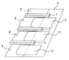
【発明が解決しようとする課題】
この従来の表示パネルにおいては、図1に示すように、陰極の金属電極9は隔壁7で分離形成されている。図示されるように、電極全体の低抵抗化又は外部への引き出しのため陰極の金属電極9上に電導線膜11をそれぞれ形成する場合がある。
【0005】
図2に示すように、表示パネルの製造工程において、電導線膜11のパターンが陰極の金属電極9から陰極と略直交する方向にずれる事がある。すると隔壁7を跨いで電導線膜11が形成されてしまう。このような状態では、1つの電導線膜11により隣接する陰極9同士の短絡が発生じる。
本発明は、このような問題を解決すべくなされ、本発明の目的は、信頼性の高い有機EL表示パネルを提供することにある。
【0006】
【課題を解決するための手段】
本発明の有機エレクトロルミネッセンス表示パネルは、複数の発光部からなる画像表示配列領域を有している有機エレクトロルミネッセンス表示パネルであって、
表面上にて前記発光部に対応する複数の第1表示電極が形成された基板と、
少なくとも前記第1表示電極の一部分を露出せしめる前記基板上に突出する複数の電気絶縁性の隔壁と、
露出した前記第1表示電極の部分の各々上に形成された少くとも1層の有機エレクトロルミネッセンス媒体の薄膜と、
各々が前記隔壁間において前記有機エレクトロルミネッセンス媒体の薄膜上に形成された複数の第2表示電極と、
各々が前記第2表示電極上に形成され前記隔壁間から前記画像表示配列領域の外部へ伸長する複数の電導線膜と、からなり、
前記隔壁は、前記画像表示配列領域の外部へ伸長しかつ前記隔壁の伸長方向に対して略直交する方向における前記隔壁の幅より大なる幅を有する隔壁端部を有することを特徴とする。
【0007】
【作用】
本発明の有機EL表示パネルによれば、電導線膜パターンがずれて隔壁を跨いで電導線膜が形成されてしまっても、隔壁端部は、陰極と略直交する方向において隔壁は幅より大となっている幅を有するので、この隔壁端部形状によって、1つの電導線膜において1つの陰極上に形成された部分と隣接する陰極上に形成された部分とは電気的に絶縁される。
【0008】
また、陰極下部に陰極が形成される有機EL表示パネルにおいて、隣接する隔壁同士を隔壁端部で結合するようにしているので、電導線膜がずれても隔壁端部の結合部分で隣接する陰極同士の短絡を防止できる。
【0009】
【発明の実施の形態】
以下に、本発明による実施例を図面を参照しつつ説明する。
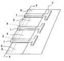
図3に示すように、実施例の有機EL表示パネルは、基板2上に例えばマトリクスは位置の複数の有機EL素子OELEを備えている。複数の有機EL素子が配列されている領域が画像表示配列領域となる。有機EL素子OELEの各々は基板2上に順に積層された第1表示電極、少くとも1層の有機EL媒体の薄膜、第2表示電極からなっている。有機EL表示パネルは電気絶縁性の隔壁7をも備えており、隔壁7が基板2上にて隣接する有機EL素子OELEの間を通過して伸長して形成されかつ突出してこれらを分離する。電導線膜11が隔壁7の伸長方向に略平行して第2表示電極9上に形成され、有機EL素子の外部へ伸長するようになっている。
【0010】
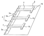
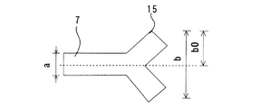
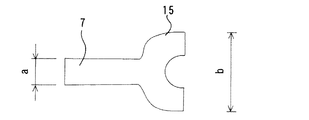
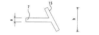
隔壁の端部は、図4に示すように、電導線膜11が隔壁7の伸長方向に対し略垂直方向に位置ずれを生じた場合に隣接する第2表示電極9のすくなくとも一方を電導線膜11から断線せしめる形状、例えばT字形状を有している。すなわち、図5に示すように、画像表示配列領域の外部へ伸長する隔壁7の隔壁端部15は、隔壁の伸長方向に対して略直交する方向における隔壁の幅aより大なる幅bを有している。
上記実施形態の有機EL表示パネルの製造方法を説明する。
【0011】
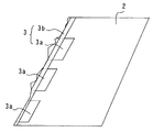
(第1表示電極ライン形成)
ガラス等の透明基板2を用意し、その主面に、図6に示すように、インジウム錫酸化物(以下、ITOという)などの高仕事関数の材料からなる複数の島状透明電極3aを画像表示配列領域となるようにマトリクス状に形成する。次に、図7に示すように、これら島状透明電極3aを水平方向に電気的に接続する金属の陽極バスライン3bを蒸着などにより形成する。陽極バスラインの幅は島状透明電極の幅よりも小とする。この島状透明電極及び陽極バスラインからなる第1表示電極ライン3は複数本で互いに平行に形成する。このように、第1表示電極ライン3は互いに平行な複数のストライプ状に配列されている。陽極バスライン材質は、Al,Cu,Auなど抵抗率の低い金属が用いられる。なお、島状透明電極3aを除き、第1表示電極ライン3上を絶縁膜で被覆することもできる。
【0012】
(隔壁形成)
つぎに、図8に示すように、第1表示電極3a、3bに対して垂直方向に伸長しかつ各々が島状透明電極間に位置するように複数の電気絶縁性の隔壁7を形成する。隔壁7は、画像表示配列領域1aの外部へ伸長しかつ隔壁の伸長方向に対して略直交する方向における隔壁の幅aより大なる幅bを有する隔壁端部15を有している。おのおのの隔壁端部15は、画像表示配列領域1aすなわち後に成膜される第2表示電極から等しい距離だけ伸長して終端するように形成する。
ここでは、隔壁を例えばフォトレジストを用い、通常のフォトリソグラフィ法等の手法を用いて形成する。隔壁7は隔壁本体及びその上部に基板に平行な方向に突出するオーバーハング部からなる断面が略T字型又は逆テーパ(逆等脚台形)の形状を有する。このようにして、少なくとも第1表示電極の一部分、特に透明電極を露出せしめかつ全体が基板上から突出する隔壁を形成する。
【0013】
隔壁7の隔壁端部15は後で形成される第2表示電極間同士の短絡防止のために画像表示配列領域の外に延在するように形成され、隔壁7の基板からの高さは、後に形成される第2表示電極の陰極9の膜厚を超える高さであればいくらでもよい。
このように、電気絶縁性の隔壁7が第1表示電極ライン3に直交するように基板2及び第1表示電極ライン3上にわたって形成され、隔壁形成工程中、隔壁7が少なくとも第1表示電極ライン3の一部分、特に島状透明電極を露出せしめるように、形成される。
【0014】
(発光層形成)
次に、各々の前記第1表示電極の一部上に、有機EL媒体を堆積し、複数の少くとも1層の有機EL媒体の薄膜を形成する工程を説明する。有機EL媒体の正孔輸送層を予め一様に形成しておく。つぎに、有機発光層を成膜し、この工程で電子輸送層も成膜できる。さらにこれらの適切な機能層間に電子或いは正孔の注入層をも成膜できる。
図9に示すように、例えば有機発光層の成膜では、マスク30の貫通開口31を、隔壁7間の露出したITO電極3に位置合わせして、隔壁上にマスクを載置して、1番目(例えば赤色発光)の有機EL媒体8aを蒸着方法を用いて所定厚さに成膜する。
次に、マスクをずらして位置合わせをした後、同様に、隔壁上にマスクを載置して2番目(例えば緑色発光)、3番目(例えば青色発光)の有機EL媒体を所定膜厚に順次成膜する。このように、1つの開口が1つの第1表示電極上からその隣接する第1表示電極上へ配置されるようにマスクを順次移動せしめる発光層形成工程を順次繰り返す。このように、有機EL媒体の薄膜は、前記有機発光層は同一の前記マスクを用いて蒸着により形成される。有機EL媒体はそれぞれ第1表示電極上に別個に並置されかつ電圧印加によりそれぞれ赤R、緑G及び青Bの色の光を発光する複数の有機発光層が形成される。
【0015】
(第2表示電極形成)
有機EL媒体の薄膜上に、図10に示すように、垂直方向に伸長する複数の第2表示電極9の陰極を蒸着などにより形成し、前記第1表示電極との各交差部にて発光部を画定する。
隔壁7の頂上及びオーバーハング部は、金属蒸気流れに対して屋根及び軒となり、隔壁7の頂上及びオーバーハング部上に堆積した金属膜50が第2表示電極9から離れているので、第2表示電極ライン9間の短絡を防止できる。また、金属蒸気の略垂直入射により、隔壁のオーバーハング部7aで複数の陰極の第2表示電極ライン9が分断され、電気的に絶縁されだけでなく、図11に示すように、金属蒸気流が隔壁のオーバーハング部7aを回り込む程度が、有機EL媒体材料粒子流の回り込む程度よりも小さいので、有機EL媒体8が第2表示電極ライン9からはみ出し、陰極9とITO陽極3との短絡を生じさせない。
【0016】
このように第1及び第2表示電極ラインが交差して挾まれた有機EL媒体の部分が、発光部に対応する。この実施例の有機EL表示パネルにおいて、基板及び第1表示電極が透明であり、発光は基板側から放射される。逆に、他の実施例の有機EL表示パネルにおいて、第2表示電極を透明材料で構成して、発光を第2表示電極側から放射させることもできる。
【0017】
(電導線膜形成)
つぎに、図3に示したように、マスクを用いた真空蒸着などにより、第2表示電極9上において、隔壁7間から画像表示配列領域1aの外部へ伸長する電導線膜11を形成する。
ここで、電導線膜11が隔壁7の伸長方向に対し略垂直方向に位置ずれを生じた場合においても、図4に示したように、隣接する第2表示電極9の一方を電導線膜11から断線せしめる形状、例えばT字形状を隔壁端部が有しているので、第2表示電極9間の短絡が防止され、電導線膜11のパターンの位置決め精度許容値が緩和される。
【0018】
このようにして、第2表示電極上に電導線膜を形成した後、防湿処理及び封止してフルカラーの有機EL表示パネルが得られる。図12に示すように、有機EL表示パネルは、基板2上にマトリクス状に配置されかつ各々が赤R、緑G及び青Bの発光部からなる発光画素1の複数からなる画像表示配列領域1aを有している。第1表示電極ライン3と垂直方向の第2表示電極ライン9との交差する部分の透明電極3a上で発光部が形成される。
【0019】
(他の隔壁端部の実施の形態)
隔壁端部15は図13に示すように、T字形状だけでなく、隔壁端部15は、隔壁の幅aより大なる幅bを有するとともに隔壁の伸張方向の中心線から両側に向かって等しい距離の半幅b0を有している形状例えば図14〜図33に示す略対称な形状や、図34〜図36に示すように非対称な形状を有しているものが好ましい。略対称な形状を有しているものが好ましい。
さらに、図37及び図38に示すように、隔壁端部15は、隔壁の伸張方向の中心線から両側に向かって異なる距離の半幅b1及びb2(b1>b2=0又はb1>b2>0)を有していてもよい。これらの実施形態によれば、電導線膜11の成膜工程において、マスクパターンの位置ズレに一定方向性がある場合に、成膜された電導線膜の幅が細くならない効果がある。
【0020】
また、他の実施形態では、図39に示すように、隣接する隔壁端部15は、第2表示電極9からの異なる距離はなれるように形成されている。すなわち、隣接する隔壁端部15の第2表示電極9からの距離の差Cがゼロを越えるように、それぞれ隔壁7の隔壁端部15を配置する。これにより、隣接する隔壁端部15の第2表示電極9からの距離が等しい場合の隣接する隔壁端部15の間の距離d1よりも大なる距離d2を確保できる。よって、電導線膜11が位置ずれなく成膜された時に、電導線膜の幅が細くなることが緩和される。
【0021】
他の実施形態によれば、隣接する隔壁端部15の第2表示電極9からの距離が等しい場合であっても、図40に示すように、隔壁端部15の位置に比べて第2表示電極9からの異なる距離Cだけはなれた位置に形成されかつ隔壁端部15が隔壁の幅より大なる幅を有する第2幅部分15aを有しているならば、上記同様に、電導線膜11が位置ずれなく成膜された時に、電導線膜11の幅が細くなることが緩和される効果が得られる。
【0022】
図40に示す第2幅部分15aを有する隔壁端部15の他の形状を、図41〜図47に示す。これらの場合でも、上記同様に、電導線膜11が位置ずれなく成膜された時に、電導線膜11の幅が細くなることが緩和される効果が得られる。
さらなる他の実施形態によれば、図48に示すように、隔壁7間における第2表示電極9に接続されるように、例えば、有機EL媒体の薄膜8と第2表示電極9との間に形成された第2表示電極の一部として働く陰極バスライン9aを有する以外、上記実施形態と同様の構成の有機EL表示パネルも提供され得る。
【0023】
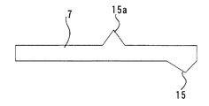
さらに、この実施形態では、図48に示すように、隣接する隔壁端部15は結合された一体化された隔壁端部15aとすることもできる。これによれば、図49に示すように、電導線膜11が隔壁7の伸長方向に対し略垂直方向に位置ずれを生じた場合でも、隣接する第2表示電極9は隣接する電導線膜11から完全に断線せしめることができる。
【0024】
なお、この実施の形態の有機EL媒体8の構造を、RGBの3組でなく、1組あるいは2組にすれば、それぞれ単色表示パネル、マルチカラー表示パネルが実現できることは明らかである。また、島状透明電極3aと陽極バスライン3bを1つにまとめ、ストライプ状透明電極とすることもできる。また、透明電極をストライプ状に形成し、陽極バスライン3aを省略することもできる。
【図面の簡単な説明】
【図1】 有機EL表示パネルの概略一部切欠拡大部分斜視図。
【図2】 有機EL表示パネルの概略一部切欠拡大部分斜視図。
【図3】 本発明による有機EL表示パネルの概略一部切欠拡大部分斜視図。
【図4】 本発明による有機EL表示パネルの概略一部切欠拡大部分斜視図。
【図5】 本発明による有機EL表示パネルの概略一部切欠拡大部分平面図。
【図6】 本発明による実施例の有機EL表示パネル製造工程における基板の概略部分斜視図。
【図7】 本発明による実施例の有機EL表示パネル製造工程における基板の概略部分斜視図。
【図8】 本発明による実施例の有機EL表示パネル製造工程における基板の概略部分斜視図。
【図9】 本発明による実施例の有機EL表示パネル製造工程における基板の概略部分斜視図。
【図10】 本発明による実施例の有機EL表示パネル製造工程における基板の概略部分斜視図。
【図11】 本発明による実施例の有機EL表示パネル製造工程における基板の概略部分拡大断面図。
【図12】 基板側から見た本発明による有機EL表示パネルの概略一部切欠拡大部分平面図。
【図13】 本発明による実施例の有機EL表示パネルにおける隔壁及びその端部の概略部分平面図。
【図14】 本発明による他の実施例の有機EL表示パネルにおける隔壁及びその端部の概略部分平面図。
【図15】 本発明による他の実施例の有機EL表示パネルにおける隔壁及びその端部の概略部分平面図。
【図16】 本発明による他の実施例の有機EL表示パネルにおける隔壁及びその端部の概略部分平面図。
【図17】 本発明による他の実施例の有機EL表示パネルにおける隔壁及びその端部の概略部分平面図。
【図18】 本発明による他の実施例の有機EL表示パネルにおける隔壁及びその端部の概略部分平面図。
【図19】 本発明による他の実施例の有機EL表示パネルにおける隔壁及びその端部の概略部分平面図。
【図20】 本発明による他の実施例の有機EL表示パネルにおける隔壁及びその端部の概略部分平面図。
【図21】 本発明による他の実施例の有機EL表示パネルにおける隔壁及びその端部の概略部分平面図。
【図22】 本発明による他の実施例の有機EL表示パネルにおける隔壁及びその端部の概略部分平面図。
【図23】 本発明による他の実施例の有機EL表示パネルにおける隔壁及びその端部の概略部分平面図。
【図24】 本発明による他の実施例の有機EL表示パネルにおける隔壁及びその端部の概略部分平面図。
【図25】 本発明による他の実施例の有機EL表示パネルにおける隔壁及びその端部の概略部分平面図。
【図26】 本発明による他の実施例の有機EL表示パネルにおける隔壁及びその端部の概略部分平面図。
【図27】 本発明による他の実施例の有機EL表示パネルにおける隔壁及びその端部の概略部分平面図。
【図28】 本発明による他の実施例の有機EL表示パネルにおける隔壁及びその端部の概略部分平面図。
【図29】 本発明による他の実施例の有機EL表示パネルにおける隔壁及びその端部の概略部分平面図。
【図30】 本発明による他の実施例の有機EL表示パネルにおける隔壁及びその端部の概略部分平面図。
【図31】 本発明による他の実施例の有機EL表示パネルにおける隔壁及びその端部の概略部分平面図。
【図32】 本発明による他の実施例の有機EL表示パネルにおける隔壁及びその端部の概略部分平面図。
【図33】 本発明による他の実施例の有機EL表示パネルにおける隔壁及びその端部の概略部分平面図。
【図34】 本発明による他の実施例の有機EL表示パネルにおける隔壁及びその端部の概略部分平面図。
【図35】 本発明による他の実施例の有機EL表示パネルにおける隔壁及びその端部の概略部分平面図。
【図36】 本発明による他の実施例の有機EL表示パネルにおける隔壁及びその端部の概略部分平面図。
【図37】 本発明による他の実施例の有機EL表示パネルにおける隔壁及びその端部の概略部分平面図。
【図38】 本発明による他の実施例の有機EL表示パネルにおける隔壁及びその端部の概略部分平面図。
【図39】 本発明による他の実施例の有機EL表示パネルにおける隔壁及びその端部の概略部分平面図。
【図40】 本発明による他の実施例の有機EL表示パネルにおける隔壁及びその端部の概略部分平面図。
【図41】 本発明による他の実施例の有機EL表示パネルにおける隔壁及びその端部の概略部分平面図。
【図42】 本発明による他の実施例の有機EL表示パネルにおける隔壁及びその端部の概略部分平面図。
【図43】 本発明による他の実施例の有機EL表示パネルにおける隔壁及びその端部の概略部分平面図。
【図44】 本発明による他の実施例の有機EL表示パネルにおける隔壁及びその端部の概略部分平面図。
【図45】 本発明による他の実施例の有機EL表示パネルにおける隔壁及びその端部の概略部分平面図。
【図46】 本発明による他の実施例の有機EL表示パネルにおける隔壁及びその端部の概略部分平面図。
【図47】 本発明による他の実施例の有機EL表示パネルにおける隔壁及びその端部の概略部分平面図。
【図48】 本発明による他の実施例の有機EL表示パネルの概略一部切欠拡大部分斜視図。
【図49】 本発明による他の実施例の有機EL表示パネルの概略一部切欠拡大部分斜視図。
【符号の説明】
1 発光画素
2 基板
3 第1表示電極ライン
3a 島状透明電極
3b 陽極バスライン
7 隔壁
7a オーバーハング部
8 有機EL媒体
9 第2表示電極ライン
15 隔壁端部[0001]
BACKGROUND OF THE INVENTION
The present invention relates to an organic EL device including a light-emitting layer (hereinafter referred to as an organic light-emitting layer) made of a thin film of an organic compound material that exhibits electroluminescence (hereinafter also referred to as EL) that emits light by current injection. The present invention relates to an organic EL display panel in which organic EL elements are formed on a substrate with a predetermined pattern and a method for manufacturing the same.
[0002]
[Prior art]
The organic EL element is configured by sequentially laminating a transparent electrode of an anode, an organic EL medium, and a metal electrode of a cathode on a transparent substrate. For example, the organic EL medium is a single layer of an organic light emitting layer, or a medium of a three-layer structure of an organic hole transport layer, an organic light emitting layer and an organic electron transport layer, or a layer structure of an organic hole transport layer and an organic light emitting layer. And a laminated medium in which an electron or hole injection layer is inserted between these appropriate layers.
[0003]
The organic EL display panel is obtained by forming a plurality of organic EL elements on a substrate with a predetermined pattern. For example, this matrix display panel is disclosed in Japanese Patent Laid-Open No. 9-102393. This full-color display is a light emitting device having an image display array composed of light emitting pixels of a plurality of organic EL elements arranged in intersecting rows and columns. For example, the matrix display type is configured by sequentially laminating a row electrode including a transparent electrode layer, an organic EL medium, and a column electrode including a metal electrode layer intersecting the row electrode. The row electrodes are each formed in a strip shape and are arranged so as to be parallel to each other at a predetermined interval, and the same applies to the column electrodes. Thus, the matrix display type display panel has an image display array composed of light emitting pixels of a plurality of organic EL elements formed at intersections of a plurality of row and column electrodes.
[0004]
[Problems to be solved by the invention]
In this conventional display panel, as shown in FIG. 1, the
[0005]
As shown in FIG. 2, in the manufacturing process of the display panel, the pattern of the
The present invention has been made to solve such problems, and an object of the present invention is to provide a highly reliable organic EL display panel.
[0006]
[Means for Solving the Problems]
The organic electroluminescence display panel of the present invention is an organic electroluminescence display panel having an image display arrangement region composed of a plurality of light emitting portions,
A substrate on which a plurality of first display electrodes corresponding to the light emitting portion are formed;
A plurality of electrically insulating partition walls protruding on the substrate exposing at least a portion of the first display electrode;
A thin film of at least one organic electroluminescent medium formed on each of the exposed portions of the first display electrode;
A plurality of second display electrodes each formed on the thin film of the organic electroluminescence medium between the partition walls;
Each comprising a plurality of conductive wire films formed on the second display electrode and extending from between the partition walls to the outside of the image display arrangement region,
The partition wall has a partition wall end that extends to the outside of the image display arrangement region and has a width larger than the width of the partition wall in a direction substantially orthogonal to the extending direction of the partition wall.
[0007]
[Action]
According to the organic EL display panel of the present invention, even if the conductive wire film pattern is shifted and the conductive wire film is formed across the barrier rib, the barrier rib end is larger than the width in the direction substantially perpendicular to the cathode. Therefore, a portion formed on one cathode and a portion formed on an adjacent cathode in one conductive wire film are electrically insulated by the shape of the partition wall end.
[0008]
Further, in the organic EL display panel in which the cathode is formed in the lower part of the cathode, the adjacent partition walls are coupled at the partition end portions. Therefore, even if the conductive wire film is displaced, the adjacent cathodes at the coupled portion of the partition end portions. Short circuit between each other can be prevented.
[0009]
DETAILED DESCRIPTION OF THE INVENTION
Embodiments according to the present invention will be described below with reference to the drawings.
As shown in FIG. 3, the organic EL display panel of the embodiment includes a plurality of organic EL elements OELE whose positions are, for example, a matrix on a
[0010]
As shown in FIG. 4, at least one of the adjacent
A method for manufacturing the organic EL display panel of the above embodiment will be described.
[0011]
(First display electrode line formation)
A
[0012]
(Partition formation)
Next, as shown in FIG. 8, a plurality of electrically insulating
Here, the partition wall is formed using, for example, a photoresist and a technique such as a normal photolithography method. The
[0013]
The
In this manner, the electrically insulating
[0014]
(Light emitting layer formation)
Next, a process of depositing an organic EL medium on a part of each of the first display electrodes to form a plurality of at least one organic EL medium thin film will be described. The hole transport layer of the organic EL medium is formed uniformly in advance. Next, an organic light emitting layer is formed, and an electron transport layer can also be formed in this step. Further, an electron or hole injection layer can be formed between these appropriate functional layers.
As shown in FIG. 9, for example, in forming an organic light emitting layer, the through opening 31 of the
Next, after aligning the position by shifting the mask, similarly, the mask is placed on the partition wall, and the second (for example, green light emission) and third (for example, blue light emission) organic EL media are sequentially formed in a predetermined film thickness. Form a film. In this manner, the light emitting layer forming step of sequentially moving the mask so that one opening is disposed on one first display electrode and on the adjacent first display electrode is sequentially repeated. As described above, the organic EL medium thin film is formed by vapor deposition using the same mask as the organic light emitting layer. Each of the organic EL media is separately juxtaposed on the first display electrode, and a plurality of organic light emitting layers that emit light of red R, green G, and blue B are formed by applying a voltage.
[0015]
(Second display electrode formation)
On the thin film of the organic EL medium, as shown in FIG. 10, the cathodes of the plurality of
The top and the overhang portion of the
[0016]
Thus, the portion of the organic EL medium sandwiched between the first and second display electrode lines corresponds to the light emitting portion. In the organic EL display panel of this embodiment, the substrate and the first display electrode are transparent, and light emission is emitted from the substrate side. On the contrary, in the organic EL display panel of another embodiment, the second display electrode can be made of a transparent material, and light emission can be emitted from the second display electrode side.
[0017]
(Conductive wire film formation)
Next, as shown in FIG. 3, a
Here, even when the
[0018]
Thus, after forming a conductive wire film on the second display electrode, a moisture-proof treatment and sealing are performed to obtain a full-color organic EL display panel. As shown in FIG. 12, the organic EL display panel is arranged in a matrix on the
[0019]
(Another embodiment of the partition wall end)
As shown in FIG. 13, the partition
Further, as shown in FIGS. 37 and 38, the partition
[0020]
In another embodiment, as shown in FIG. 39, adjacent partition
[0021]
According to another embodiment, even when the distance between the adjacent partition
[0022]
Other shapes of the
According to still another embodiment, as shown in FIG. 48, for example, between the
[0023]
Furthermore, in this embodiment, as shown in FIG. 48, the adjacent partition
[0024]
It is obvious that a monochromatic display panel and a multicolor display panel can be realized if the structure of the
[Brief description of the drawings]
FIG. 1 is a partially cutaway enlarged partial perspective view of an organic EL display panel.
FIG. 2 is a partially cutaway enlarged partial perspective view of the organic EL display panel.
FIG. 3 is a schematic partially cutaway enlarged perspective view of an organic EL display panel according to the present invention.
FIG. 4 is a partially cutaway enlarged partial perspective view of the organic EL display panel according to the present invention.
FIG. 5 is a schematic partially cutaway enlarged plan view of an organic EL display panel according to the present invention.
FIG. 6 is a schematic partial perspective view of a substrate in an organic EL display panel manufacturing process according to an embodiment of the present invention.
FIG. 7 is a schematic partial perspective view of a substrate in an organic EL display panel manufacturing process according to an embodiment of the present invention.
FIG. 8 is a schematic partial perspective view of a substrate in an organic EL display panel manufacturing process of an embodiment according to the present invention.
FIG. 9 is a schematic partial perspective view of a substrate in an organic EL display panel manufacturing process according to an embodiment of the present invention.
FIG. 10 is a schematic partial perspective view of a substrate in an organic EL display panel manufacturing process according to an embodiment of the present invention.
FIG. 11 is a schematic partially enlarged cross-sectional view of a substrate in an organic EL display panel manufacturing process according to an embodiment of the present invention.
FIG. 12 is a schematic partially cutaway enlarged plan view of an organic EL display panel according to the present invention as viewed from the substrate side.
FIG. 13 is a schematic partial plan view of a partition and its end in an organic EL display panel according to an embodiment of the present invention.
FIG. 14 is a schematic partial plan view of a partition and an end portion of an organic EL display panel according to another embodiment of the present invention.
FIG. 15 is a schematic partial plan view of a partition and its end in an organic EL display panel according to another embodiment of the present invention.
FIG. 16 is a schematic partial plan view of a partition and its end in an organic EL display panel according to another embodiment of the present invention.
FIG. 17 is a schematic partial plan view of a partition and its end in an organic EL display panel according to another embodiment of the present invention.
FIG. 18 is a schematic partial plan view of a partition and its end in an organic EL display panel according to another embodiment of the present invention.
FIG. 19 is a schematic partial plan view of a partition and its end in an organic EL display panel according to another embodiment of the present invention.
FIG. 20 is a schematic partial plan view of a partition and its end in an organic EL display panel according to another embodiment of the present invention.
FIG. 21 is a schematic partial plan view of a partition and its end in an organic EL display panel according to another embodiment of the present invention.
FIG. 22 is a schematic partial plan view of a partition and its end in an organic EL display panel according to another embodiment of the present invention.
FIG. 23 is a schematic partial plan view of a partition and its end in an organic EL display panel according to another embodiment of the present invention.
FIG. 24 is a schematic partial plan view of a partition and its end in an organic EL display panel according to another embodiment of the present invention.
FIG. 25 is a schematic partial plan view of a partition and its end in an organic EL display panel according to another embodiment of the present invention.
FIG. 26 is a schematic partial plan view of a partition and its end in an organic EL display panel according to another embodiment of the present invention.
FIG. 27 is a schematic partial plan view of a partition and its end in an organic EL display panel according to another embodiment of the present invention.
FIG. 28 is a schematic partial plan view of a partition and its end in an organic EL display panel according to another embodiment of the present invention.
FIG. 29 is a schematic partial plan view of a partition wall and its end in an organic EL display panel according to another embodiment of the present invention.
FIG. 30 is a schematic partial plan view of a partition and its end in an organic EL display panel according to another embodiment of the present invention.
FIG. 31 is a schematic partial plan view of a partition and its end in an organic EL display panel according to another embodiment of the present invention.
FIG. 32 is a schematic partial plan view of a partition and its end in an organic EL display panel according to another embodiment of the present invention.
FIG. 33 is a schematic partial plan view of a partition and its end in an organic EL display panel according to another embodiment of the present invention.
FIG. 34 is a schematic partial plan view of a partition and its end in an organic EL display panel according to another embodiment of the present invention.
FIG. 35 is a schematic partial plan view of a partition and its end in an organic EL display panel according to another embodiment of the present invention.
FIG. 36 is a schematic partial plan view of a partition and its end in an organic EL display panel according to another embodiment of the present invention.
FIG. 37 is a schematic partial plan view of a partition and its end in an organic EL display panel according to another embodiment of the present invention.
FIG. 38 is a schematic partial plan view of a partition and its end in an organic EL display panel according to another embodiment of the present invention.
FIG. 39 is a schematic partial plan view of a partition and its end in an organic EL display panel according to another embodiment of the present invention.
FIG. 40 is a schematic partial plan view of a partition wall and an end thereof in an organic EL display panel according to another embodiment of the present invention.
FIG. 41 is a schematic partial plan view of a partition and its end in an organic EL display panel according to another embodiment of the present invention.
FIG. 42 is a schematic partial plan view of a partition and its end in an organic EL display panel according to another embodiment of the present invention.
FIG. 43 is a schematic partial plan view of a partition and an end portion of an organic EL display panel according to another embodiment of the present invention.
FIG. 44 is a schematic partial plan view of a partition and its end in an organic EL display panel according to another embodiment of the present invention.
FIG. 45 is a schematic partial plan view of a partition and its end in an organic EL display panel according to another embodiment of the present invention.
FIG. 46 is a schematic partial plan view of a partition and its end in an organic EL display panel according to another embodiment of the present invention.
FIG. 47 is a schematic partial plan view of a partition and its end in an organic EL display panel according to another embodiment of the present invention.
FIG. 48 is a schematic partially cutaway enlarged perspective view of an organic EL display panel according to another embodiment of the present invention.
FIG. 49 is a partially cutaway enlarged partial perspective view of an organic EL display panel according to another embodiment of the present invention.
[Explanation of symbols]
DESCRIPTION OF
Claims (12)
表面上にて前記発光部に対応する複数の第1表示電極が形成された基板と、少なくとも前記第1表示電極の一部分を露出せしめる前記基板上に突出する複数の電気絶縁性の隔壁と、
露出した前記第1表示電極の部分の各々上に形成された少くとも1層の有機エレクトロルミネッセンス媒体の薄膜と、
各々が前記隔壁間において前記有機エレクトロルミネッセンス媒体の薄膜上に形成された複数の第2表示電極と、
各々が前記第2表示電極上に形成され前記隔壁間から前記画像表示配列領域の外部へ伸長する複数の電導線膜と、からなり、
前記隔壁は、前記画像表示配列領域の外部へ伸長しかつ前記隔壁の伸長方向に対して略直交する方向における前記隔壁の幅より大なる幅を有する隔壁端部を有することを特徴とする有機エレクトロルミネッセンス表示パネル。An organic electroluminescence display panel having an image display array region composed of a plurality of light emitting units,
A substrate on which a plurality of first display electrodes corresponding to the light emitting portion are formed, and a plurality of electrically insulating partitions protruding on the substrate exposing at least a part of the first display electrodes;
A thin film of at least one organic electroluminescent medium formed on each of the exposed portions of the first display electrode;
A plurality of second display electrodes each formed on the thin film of the organic electroluminescence medium between the partition walls;
Each comprising a plurality of conductive wire films formed on the second display electrode and extending from between the partition walls to the outside of the image display arrangement region,
The partition includes an end of a partition that extends to the outside of the image display array region and has a width larger than the width of the partition in a direction substantially orthogonal to the extending direction of the partition. Luminescence display panel.
基板上において、前記発光部に対応する複数の第1表示電極を形成する工程と、
前記基板上において、少なくとも前記第1表示電極の一部分を露出せしめかつ突出する複数の電気絶縁性の隔壁を形成する工程と、
露出した前記第1表示電極の部分の各々上に少くとも1層の有機エレクトロルミネッセンス媒体の薄膜を形成する工程と、
前記隔壁間において前記有機エレクトロルミネッセンス媒体の薄膜上に複数の第2表示電極を形成する工程と、前記第2表示電極上において、前記隔壁間から前記画像表示配列領域の外部へ伸長する電導線膜を形成する工程と、からなり、
前記隔壁を形成する工程において、前記画像表示配列領域の外まで伸長しかつ前記隔壁の伸長方向に対して略直交する方向における前記隔壁の幅より大なる幅を有する前記隔壁の隔壁端部を形成することを特徴とする有機エレクトロルミネッセンス表示パネルの製造方法。A method for producing an organic electroluminescence display panel having an image display array region composed of a plurality of light emitting portions,
Forming a plurality of first display electrodes corresponding to the light emitting portion on a substrate;
Forming a plurality of electrically insulating barrier ribs on the substrate, exposing at least a portion of the first display electrode and protruding;
Forming at least one layer of an organic electroluminescent medium thin film on each exposed portion of the first display electrode;
Forming a plurality of second display electrodes on the thin film of the organic electroluminescence medium between the partition walls, and a conductive wire film extending from the partition walls to the outside of the image display arrangement region on the second display electrodes. And a process of forming
In the step of forming the partition walls, partition wall end portions of the partition walls that extend outside the image display arrangement region and have a width greater than the width of the partition walls in a direction substantially perpendicular to the extending direction of the partition walls are formed. A manufacturing method of an organic electroluminescence display panel.
Priority Applications (1)
| Application Number | Priority Date | Filing Date | Title |
|---|---|---|---|
| JP2000039178A JP4478274B2 (en) | 2000-02-17 | 2000-02-17 | Organic electroluminescence display panel and manufacturing method thereof |
Applications Claiming Priority (1)
| Application Number | Priority Date | Filing Date | Title |
|---|---|---|---|
| JP2000039178A JP4478274B2 (en) | 2000-02-17 | 2000-02-17 | Organic electroluminescence display panel and manufacturing method thereof |
Publications (3)
| Publication Number | Publication Date |
|---|---|
| JP2001230073A JP2001230073A (en) | 2001-08-24 |
| JP2001230073A5 JP2001230073A5 (en) | 2007-02-15 |
| JP4478274B2 true JP4478274B2 (en) | 2010-06-09 |
Family
ID=18562785
Family Applications (1)
| Application Number | Title | Priority Date | Filing Date |
|---|---|---|---|
| JP2000039178A Expired - Lifetime JP4478274B2 (en) | 2000-02-17 | 2000-02-17 | Organic electroluminescence display panel and manufacturing method thereof |
Country Status (1)
| Country | Link |
|---|---|
| JP (1) | JP4478274B2 (en) |
Families Citing this family (13)
| Publication number | Priority date | Publication date | Assignee | Title |
|---|---|---|---|---|
| KR100537611B1 (en) | 2002-04-10 | 2005-12-19 | 삼성에스디아이 주식회사 | Organic light emitting diode and method for producing thereof |
| KR100528910B1 (en) | 2003-01-22 | 2005-11-15 | 삼성에스디아이 주식회사 | Polymer organic light emitting diode |
| KR100499509B1 (en) | 2003-04-16 | 2005-07-05 | 엘지전자 주식회사 | Method for Fabricating Polymer Organic Electroluminescence Device |
| KR100705270B1 (en) * | 2003-07-31 | 2007-04-11 | 엘지전자 주식회사 | Organic Electro Luminescence Display Device And Fabricating Method Thereof |
| US7358526B2 (en) * | 2005-09-28 | 2008-04-15 | Osram Opto Semiconductors Gmbh | OLED separating structures |
| KR100738224B1 (en) * | 2006-03-31 | 2007-07-12 | 엘지전자 주식회사 | Light emitting diodes |
| WO2007114536A1 (en) * | 2006-04-05 | 2007-10-11 | Daewoo Electronics Corporation | Organic electroluminescence device and method for manufacturing same |
| JP5312909B2 (en) * | 2008-11-11 | 2013-10-09 | シャープ株式会社 | Color conversion filter panel for color organic EL display and color organic EL display |
| US20110284889A1 (en) * | 2009-01-21 | 2011-11-24 | Tohoku Pioneer Corporation | Organic el panel and method for manufacturing the same |
| JP5638599B2 (en) * | 2010-03-05 | 2014-12-10 | パイオニア株式会社 | Organic EL panel and manufacturing method thereof |
| WO2014115337A1 (en) * | 2013-01-28 | 2014-07-31 | パイオニア株式会社 | Light emission device |
| WO2014162453A1 (en) * | 2013-04-01 | 2014-10-09 | パイオニア株式会社 | Joint structure and light-emitting device |
| KR102277705B1 (en) * | 2017-06-30 | 2021-07-14 | 엘지디스플레이 주식회사 | Display device |
-
2000
- 2000-02-17 JP JP2000039178A patent/JP4478274B2/en not_active Expired - Lifetime
Also Published As
| Publication number | Publication date |
|---|---|
| JP2001230073A (en) | 2001-08-24 |
Similar Documents
| Publication | Publication Date | Title |
|---|---|---|
| JP4142117B2 (en) | Organic electroluminescence display panel and manufacturing method thereof | |
| KR100804921B1 (en) | Organic electroluminescent display panel and method of manufacturing the same | |
| JP4490646B2 (en) | Shadow mask, flat panel display manufactured using the same, and method of manufacturing the same | |
| US6297589B1 (en) | Organic electroluminescence full color display panel and method of manufacturing the same | |
| US5742129A (en) | Organic electroluminescent display panel with projecting ramparts and method for manufacturing the same | |
| JP4925566B2 (en) | Shadow mask | |
| KR101479994B1 (en) | Organic light emitting diode display and method for manufacturing the same | |
| JP3813217B2 (en) | Method for manufacturing organic electroluminescence display panel | |
| JP4230258B2 (en) | Organic EL panel and organic EL panel manufacturing method | |
| JP3570857B2 (en) | Organic EL display panel and manufacturing method thereof | |
| JP4478274B2 (en) | Organic electroluminescence display panel and manufacturing method thereof | |
| JP2001237073A (en) | Metal mask for multiple formation and manufacturing method of the same | |
| JP2008071770A (en) | Organic el display panel | |
| JP2010262920A (en) | Organic light-emitting display device | |
| JP4164910B2 (en) | Organic EL display and organic EL display manufacturing method | |
| US6717357B2 (en) | Organic electroluminescent display panel | |
| JP2006331920A (en) | Depositing mask, organic electroluminescent display device, and method of manufacturing the same | |
| US7221094B2 (en) | Electroluminescent device and method of manufacturing the same | |
| JP2000100576A5 (en) | ||
| CN113540194B (en) | Display panel and display device | |
| KR100975295B1 (en) | Electrical device and method for manufacturing an electrical device | |
| JP4392113B2 (en) | Organic electroluminescence display panel and organic electroluminescence display panel manufacturing method | |
| JPH10312884A (en) | Light emitting display panel, manufacture therefor and second electrode manufacturing mask therefor | |
| JP4494681B2 (en) | Deposited film forming method, mask used therefor, and organic electroluminescence display panel | |
| CN115943748A (en) | Display substrate, display device and manufacturing method |
Legal Events
| Date | Code | Title | Description |
|---|---|---|---|
| A521 | Request for written amendment filed |
Free format text: JAPANESE INTERMEDIATE CODE: A523 Effective date: 20061221 |
|
| A621 | Written request for application examination |
Free format text: JAPANESE INTERMEDIATE CODE: A621 Effective date: 20061221 |
|
| A977 | Report on retrieval |
Free format text: JAPANESE INTERMEDIATE CODE: A971007 Effective date: 20091113 |
|
| A131 | Notification of reasons for refusal |
Free format text: JAPANESE INTERMEDIATE CODE: A131 Effective date: 20091215 |
|
| A521 | Request for written amendment filed |
Free format text: JAPANESE INTERMEDIATE CODE: A523 Effective date: 20100215 |
|
| TRDD | Decision of grant or rejection written | ||
| A01 | Written decision to grant a patent or to grant a registration (utility model) |
Free format text: JAPANESE INTERMEDIATE CODE: A01 Effective date: 20100309 |
|
| A01 | Written decision to grant a patent or to grant a registration (utility model) |
Free format text: JAPANESE INTERMEDIATE CODE: A01 |
|
| A61 | First payment of annual fees (during grant procedure) |
Free format text: JAPANESE INTERMEDIATE CODE: A61 Effective date: 20100315 |
|
| R150 | Certificate of patent or registration of utility model |
Free format text: JAPANESE INTERMEDIATE CODE: R150 Ref document number: 4478274 Country of ref document: JP Free format text: JAPANESE INTERMEDIATE CODE: R150 |
|
| FPAY | Renewal fee payment (event date is renewal date of database) |
Free format text: PAYMENT UNTIL: 20130319 Year of fee payment: 3 |
|
| FPAY | Renewal fee payment (event date is renewal date of database) |
Free format text: PAYMENT UNTIL: 20140319 Year of fee payment: 4 |
|
| EXPY | Cancellation because of completion of term |