JP4477704B2 - Method for removing organic contaminants from semiconductor substrate surface - Google Patents
Method for removing organic contaminants from semiconductor substrate surface Download PDFInfo
- Publication number
- JP4477704B2 JP4477704B2 JP33155598A JP33155598A JP4477704B2 JP 4477704 B2 JP4477704 B2 JP 4477704B2 JP 33155598 A JP33155598 A JP 33155598A JP 33155598 A JP33155598 A JP 33155598A JP 4477704 B2 JP4477704 B2 JP 4477704B2
- Authority
- JP
- Japan
- Prior art keywords
- ozone
- removal method
- semiconductor substrate
- liquid
- additive
- Prior art date
- Legal status (The legal status is an assumption and is not a legal conclusion. Google has not performed a legal analysis and makes no representation as to the accuracy of the status listed.)
- Expired - Lifetime
Links
Images


Abstract
Description
【0001】
【発明の属する技術分野】
本発明は、半導体基板表面からの有機汚染物の除去方法に関する。本発明は、さらに複数の連続した洗浄処理、又はVIAエッチングや他のエッチング処理後の洗浄等の多くの応用に対する本発明の方法の利用に関する。
【0002】
【従来の技術】
酸化、堆積又は成長プロセス等の様々なプロセス工程の前に行われる半導体基板表面の調製が、半導体技術における最も重要な問題の一つになってきた。0.5ミクロン及び0.25ミクロン以下のデザインルールの急速な普及とともに、微小な粒子と低レベルの汚染又は不純物(〜1010atoms/cm2、そしてそれ以下)がプロセスの歩止りに重大な影響を及ぼす。半導体基板表面から除去されるべき汚染物には、金属不純物、粒子及び有機物がある。半導体基板表面の異物の汚染レベルを低減するのに通常用いられる方法は、薬品溶液にウエーハを浸漬する方法である。
【0003】
有機物は、半導体ウエーハの表面から除去されなくてはならない汚染物の一つである。前洗浄段階においては、吸収された有機分子がウエーハ表面と洗浄用薬品との接触を妨げるため、不均一なエッチングやウエーハ表面の不均一な洗浄の原因となる。汚染のないウエーハ表面を実現するためには、有機不純物は他のウエーハ洗浄プロセスの前に除去されなくてならない。従来の湿式洗浄プロセスは、有機物を除去するための硫酸過酸化物混合物(SPM)の利用を含む。しかし、SPMは高価な薬品を使用し、そして高温で用いる必要があり、また化学廃棄物処理の問題を引き起こす。
【0004】
有機汚染の他の発生源は、標準的なICプロセスの流れにおいても起こる。その例としては、半導体基板の上の堆積されるフォトレジスト層又はフルオロカーボンポリマーの残留物がある。フルオロカーボンポリマーの残留物は、半導体(シリコン)半導体基板をドライな酸化物エッチング処理した時にできる。通常のフルオロカーボン気体を用いる酸化物エッチングでは、垂直の側壁プロファイルとフォトレジストマスクと下層膜に対するエッチングの選択性を高めるために、ポリマーを意図的に生成させる。SiO2−Si系のおけるエッチング選択性は、フルオロカーボンを基剤とするポリマーの生成を通じて特定のプロセス条件で達成される。重合反応は、Siの上で起こり易く、保護被膜を形成し、SiとSiO2間のエッチング選択性をもたらす。選択エッチングの後、レジストとポリマー状残留物は表面から除去される必要がある。もし、そのポリマーが次の金属堆積の前に完全に除去されないと、ポリマーはスパッタ金属原子と混ざり合い、信頼性に影響を与える高抵抗の物質を形成する。ポリマーの除去の方法は、プラズマエッチングの化学的作用、プラズマ源及び堆積フィルムの組成に依存する。しかし、乾式プロセスにおいては、O2又はH2を含む気体がフルオロカーボンポリマーの除去に用いられてきた。湿式の洗浄技術においては、アミンを基剤とする溶媒(米国特許第5,279,771号公報 と 米国特許第5,308,745号公報 )がよく使われている。有機フォトレジストの除去には、通常、湿式や乾式の酸化的な化学的作用(すなわち、O2プラズマ、SPM)又は溶媒剥離に基づく溶解プロセスが含まれる。これらのプロセスは高価であり、また廃棄物処理に関しては環境的に有害なものである。
【0005】
【発明が解決しようとする課題】
Si表面から有機汚染物(フォトレジストやエッチングの残留物)を除去する他の有効な洗浄方法を見い出す過程において、オゾン処理の化学的作用の利用が検討された。オゾンは、その強力な酸化力により、排水処理や飲料水の殺菌の分野で広く使われている。さらにオゾンの利点として、分解及び/又は反応の後の残留物(H2O、CO2、O2)が無害であることが挙げられる。オゾンの有機汚染物に対する酸化作用は、2つの異なる酸化経路、直接酸化又は間接的な酸化を含むものと一般に考えられている。直接酸化又はオゾン分解は第1の酸化剤として、分子状オゾンを含む。それは、まず炭素-炭素二重結合で起きる。このタイプの酸化は排水が低いpH域にある時に、起き易い。間接的な酸化は、第1の酸化剤のような第2の酸化剤を含む(たとえば、OHラジカル)。このタイプの酸化は、より反応性が高いが、あまり鋭敏ではなく、OHラジカルの生成し易い、高いpH、高温、促進剤(たとえば、H2O2)の添加、紫外線照射のような条件において、起き易い。実際の状況においては、オゾンに対して異なる反応性を有する汚染物の混合物が処理の対象となることが多い。しかし、いずれの酸化経路も同時に起き、間接的な酸化を進行させるには、分子状オゾンに対して高い反応性を有する有機汚染物の除去効率を犠牲にする必要がある。オゾン処理の化学的作用により、有機物の除去効率を最適化するためには、両方の酸化経路に影響を与えるパラメータを確認することが重要である。
【0006】
近年、オゾンは、その強い酸化力ゆえに、マイクロエレクトロニクス産業に導入された。オゾンが水に溶解した時、その自己分解時間は気相における場合に比べて速くなる。自己分解の間に、オゾンは反応の副生物としてOHラジカルを生成させる。G.AlderとR.Hill(J.Am.Chem.Soc.1950,72(1984)))によれば、これは有機物の分解によるものと信じられている。
【0007】
米国特許第5,464,480号公報は、半導体ウエハーから有機物を除去する方法を開示している。ウエハーを、1℃から15℃の温度範囲で、オゾンを含む水溶液に接触せしめる。ウエハーは、脱イオン水を含むタンクの中に置かれる。そしてウエハーから有機物を除去するのに十分な時間、オゾンを室温以下の脱イオン水の中に拡散させる。その間脱イオン水の温度は1℃から15℃の間に保つ。次に、ウエハーを脱イオン水ですすぐ。溶液の温度を1℃から15℃の間に保つ理由は、ウエハー上のすべての有機物を酸化し不溶性の気体にするため、十分に高濃度のオゾンを水の中に存在させる必要があるからである。
【0008】
欧州特許出願EP−A−0548596号は、洗浄工程において、いろいろな液状の薬品や超純水又はオゾンを含む気体と超純水からなる混合相流体を、オゾン気体を満たした処理室で半導体基板又は半導体ウエハーの上に噴霧する、スプレーツールプロセスを開示している。常に処理液の薄膜を新しくするためと、望ましくない物質を遠心力による除去を促進するため、回転させることが必要である。
【0009】
米国特許第5,181,985号公報は、湿式法で薬品を用いる半導体ウエハーの表面処理プロセスを開示している。それによれば、1つ又はそれ以上の液状の化学的に活性な物質を含む水相が、霧のように微細に分離した液体の状態でウエハー表面上で反応する。そのプロセスは、ウエハー表面に霧状の水を噴霧する工程と、半導体ウエハー表面で気相と液相との相互作用を起こすため、霧状の水と結合するように気体状の化学的に活性な物質を導入する工程とからなる。化学的に活性な物質は、気体状のアンモニア、塩化水素、フッ化水素、オゾン、オゾン化された酸素、塩素及び臭素からなる群から選ばれる。温度10℃から90℃の水が系に導入される。
【0010】
米国特許第5,503,708号公報は、有機膜を除去する方法と装置を開示している。すなわち、アルコールと、オゾン気体又はオゾン含有気体の1つとを含む混合気体を、少なくとも半導体ウエハーを処理室内に置くまでの間、上記処理室内へ導入し、半導体ウエハーの表面に形成された有機膜と混合気体が反応するようにする。
【0011】
特開昭61−004232号公報は、半導体基板の洗浄方法を開示している。その方法は、従来技術において、シリコンウエハー上の重金属の還元に用いられる伝統的な酸-過酸化水素洗浄に代わるものとして開発された。半導体基板は、洗浄タンクに満たされたギ酸や酢酸等の有機酸の濃い溶液に浸漬され、オゾン又は酸素が溶液を撹拌するようにタンクの底から供給される。上記溶液は、温度が100から150℃の間になるように加熱される。有機廃棄物はオゾンにより酸化され、溶解させて除去される。言い換えると、この日本の刊行物は、ギ酸金属化合物や酢酸金属化合物の形にして重金属を除去する方法とオゾンにより有機廃棄物を半導体ウエハー上から除去する方法とを開示している。
【0012】
本発明は、有機汚染物質を半導体半導体基板から除去するための改良された方法を提案することを目的とする。さらに、詳しくは、本発明は、半導体基板作製に係るあらゆるプロセスで起こる、フォトレジスト、レジスト残留物、ドライエッチング残留物等の有機汚染物を半導体基板表面から除去する方法を提案することを目的とする。
【0013】
【発明を解決するための手段】
本発明の第1の形態は、半導体基板をタンクの中に保持する工程と、水蒸気、オゾン及び捕捉剤として働く添加物からなる気体混合物を上記タンクに満たす工程とからなる。
本発明及び関連する特許出願の目的において用いられるタンクという言葉は、洗浄又は有機汚染物を除去するため、物質を保持するあらゆる種類の道具又は反応容器を意味する。したがって、タンクという言葉には、従来知られているウエットベンチ(wet benches)、ベッセル(vessels)、スプレープロセッサー(spray processors)、スピニングツール(spinning tools)、シングルタンク(single tank)、シングルウエハークリーニングツール(single wafer cleaning tools)などの道具や反応容器が含まれる。
本発明の第2の形態は、半導体基板をタンクの中に保持する工程と、水、オゾン及び捕捉剤として働く添加物からなる液体を上記タンクに満たす工程と、上記液体をその沸点以下の温度に維持する工程とからなる。
本発明の第3の形態は、半導体基板をタンクの中に保持する工程と、水、オゾン及び捕捉剤として働く添加物からなる液体を上記タンクに満たす工程とからなり、上記添加物の上記液体中における割合が、上記液体の1モル重量%以下である。
【0014】
捕捉剤は、混合物又は系の他の成分による好ましくない効果を妨げるために、混合物又は液体、気体、溶液等のあらゆる系に添加される物質を意味する。
上記添加剤は、OHラジカルの捕捉剤として働くことが好ましい。ラジカルは、非荷電種(すなわち、1原子又は2原子又は多原子分子である)であり、少なくとも、1つの不対電子を有する。捕捉剤の例としては、酢酸(CH3COOH)、酢酸塩(CH3COO-)、炭酸塩(HxCO3 -(2-x))、リン酸塩(H3PO4 -(3-x))などのカルボン酸又はリン酸又はそれらの塩が挙げられる。
【0015】
本発明の第3の形態においては、シリコンを酸化する能力を有するオゾンと蒸留水との混合物を用いる。第3の形態はシリコン表面の効率的な洗浄方法に関するものであり、以下の連続した工程に関する。
工程1:シリコン表面に酸化物を成長させる。
工程2:酸化物を除去する。
工程3(必要に応じて):親水的な表面が望ましい場合、薄い絶縁酸化物層を成長させる。
工程4:シリコンウエハーを乾燥させる。
【0016】
以下の上記と異なる連続工程も用いることができる。
工程1:シリコン表面の酸化物の成長を、シリコンを酸化する能力のあるオゾンと水との流体(液体又は気体)混合物を用いて行う。流体は、さらに捕捉剤のような添加物を含んでも良い。
工程2:酸化物を、塩酸等を含有する又は含有しない希フッ酸洗浄剤中で除去する。
工程3(必要に応じて):親水的な表面が望ましい場合、薄い絶縁酸化膜を、希塩酸とオゾンの混合物のようなオゾン化された混合物中で成長させる。
工程4:マラゴンニ型の乾燥又はシリコンウエハーの加熱を伴う乾燥により、シリコンウエハーを乾燥させる。
この連続した工程は、ウエットベンチ、シングルタンク、スプレープロセッサー、シングルウエハークリーニングツールなどのあらゆる反応容器やタンクを用いて行うことができる。
【0017】
本発明は、集積回路用のシリコンウエハーの製造において用いることができる。また、本発明は、平面デイスプレイ、太陽電池の製造のような関連する分野において又はマイクロマシニングの応用において又は半導体基板表面から有機汚染物質を除去する必要のある他の分野においても用いることができる。
【0018】
【発明の実施の形態】
本発明の目的は、半導体基板表面から有機汚染物を除去する方法に関する。
上記方法は、シリコン表面からフォトレジスト及びエッチング後の有機残留物を除去するのに用いることができる。上記有機汚染物は、上記半導体基板の少なくとも一部を覆う拘束された層である。上記拘束された層の厚さは、単分子層以下から1μmの範囲である。上記方法は、気相又は液相プロセスに適用できる。
以下の説明において、気相プロセスを対象とする本発明の第1の好ましい実施形態と、液相プロセスを対象とする本発明の第2の好ましい実施形態が開示される。
【0019】
<気相プロセスを対象とする第1の好ましい実施形態>
気相プロセスにおいて、半導体基板は、水蒸気、オゾン及び捕捉剤として働く添加物を含む気体混合物と接触するように、タンクの中に置かれる。捕捉剤は、他の成分による好ましくない影響を除くために、混合物に添加される物質である。捕捉剤は、OHラジカル捕捉剤として主に働く。添加物は、カルボン酸又はリン酸又はその塩である。さらに好ましくは、添加物は、酢酸である。
【0020】
気体混合物中における添加物の割合は、好ましくは気体混合物の10モル重量%以下である。気体混合物中における添加物の割合は、より好ましくは気体混合物の1モル重量%以下である。さらにより好ましくは、気体混合物中における添加物の割合は、気体混合物の0.5モル重量%以下である。さらにより好ましくは、気体混合物中における添加物の割合は、気体混合物の0.1モル重量%以下である。
【0021】
気体混合物は、酸素、窒素、アルゴン又は他のあらゆる不活性気体を含んでもよい。気体混合物のオゾン濃度は、主に10〜15モル重量%以下である。水蒸気は、主に混合物の使用温度で飽和している。混合物の使用温度は150℃以下であり、半導体基板の温度より高いことが好ましい。
【0022】
また半導体基板を溶液で濯ぐ工程を含んでも良い。濯ぎに用いる溶液は、脱イオン水からなることが好ましい。濯ぎに用いる溶液は、さらに塩酸及び/又はフッ酸、及び/又は硝酸、及び/又は二酸化炭素、及び/又はオゾンからなっても良い。また、濯ぎに用いる溶液をメガソン超音波撹拌しても良い。
【0023】
好ましくは、本実施形態においては、タンクに少なくとも水と上記添加物からなる液体を満たす工程を含み、タンクの液面を半導体基板より下にして、液体を加熱する。それから、タンクは、添加物を含む飽和水蒸気で満たされる。タンクは、さらにオゾンで満たされる。好ましくは、オゾンは液体を通してバブリングされる。液体は、好ましくは16℃から99℃の範囲で、より好ましくは、20℃と90℃の間で加熱される。さらにより好ましくは、60℃から80℃の間で加熱される。
【0024】
湿潤オゾン気相プロセスと表示された装置構成においては、完全にオゾン拡散器を浸漬するに十分な少量の液体のみを満たした石英容器を用いることが好ましい。液体は、酢酸のような添加物を添加した脱イオン水である。液体は石英容器の上に置かれる。液体は80℃に加熱される。ウエハーは、直接液体界面の上に浸漬しないように置かれる。オゾン拡散器は、溶融シリカから組み立てられ、オゾン発生器(ソルビウス)は、オゾン量が最大になるように酸素を流しながら操作される。望ましくは、酸素流量は3l/minが用いられる。実験の間ずっと、オゾンは液体の中に直接バブリングされる(気泡は減らさない)。密閉容器で液体を加熱し、液体を通して連続的にオゾンをバブリングさせることにより、ウエハーを湿潤な周囲に存在するオゾンに曝す。気相の実験においては、作業温度は80℃、脱イオン水は酢酸で酸性にする(1/100体積比)。ウエハーは、十分に長い時間処理され、湿潤気相処理の後に濯ぐ工程を行う。実験においては、ウエハーは10分処理され、続いて脱イオン水で10分濯ぎを受ける。
【0025】
また、酢酸が添加された蒸留水(pH1以下、好ましくは16M酢酸を100倍に薄める)又は硝酸を添加した蒸留水(pH1.5以下、好ましくは16M硝酸を100倍に薄める)を含む静置した石英容器に全部が浸漬したオゾン拡散器からオゾンをバブリングさせても良い。液体は石英容器の上に置かれる。ウエハーは、その液体の上に置かれ、周囲の湿ったオゾンに50℃又は80℃で10分間曝される。
【0026】
さらに、連続する80℃、10分間の湿潤オゾン気相工程と、5%硫酸を含む過酸化水素溶液を用いる90℃、10分間の酸洗浄工程との組み合わせを含む10分間の洗浄処理を行っても良い。
【0027】
<液相プロセスを対象とする第2の好ましい実施形態>
液相プロセスにおいて、半導体基板は、水、オゾン及び捕捉剤として働く添加剤との混合物からなる液体と接触するように、タンクの中に置かれる。捕捉剤は、他の成分による好ましくない影響を除去するために混合物に添加される物質である。捕捉剤は、主にOHラジカルの捕捉剤として働く。
【0028】
添加剤は、カルボン酸又はリン酸又はそれらの塩であり、好ましくは酢酸である。液体における添加物の割合は、液体の1モル重量%以下である。好ましくは、液体における添加物の割合は、液体の0.5モル重量%以下である。さらに好ましくは、液体における添加物の割合は、液体の0.1モル重量%以下である。液体は、さらにメガソン超音波撹拌される。
【0029】
好ましくは、さらに液体をその沸点以下の温度に維持する工程を含む。液体の温度は、100℃以下であることが好ましい。さらに好ましくは、16℃から99℃の間である。さらに好ましくは、20℃と90℃の間である。さらに好ましくは、60℃と80℃の間である。
【0030】
オゾンの気泡が半導体基板に接触するように、オゾンが液体を通してバブリングされるのが好ましい。
【0031】
さらに好ましくは、さらに、半導体基板を溶液で濯ぐ工程を含む。濯ぎに用いる溶液は、脱イオン水からなることが好ましい。濯ぎに用いる溶液は、さらに塩酸及び/又はフッ酸、及び/又は硝酸、及び/又は二酸化炭素、及び/又はオゾンを含むことがより好ましい。濯ぎに用いる溶液は、メガソン超音波撹拌される。
【0032】
本実施形態において、好ましくは、以下の装置構成が用いられる。気泡試験と表示されるオゾン装置構成(浸漬型)は、7lの液体が入る石英容器とタンクの底に位置するオゾン拡散器とからなる。液体は加熱される。作業温度は、45℃である。オゾン拡散器は、溶融シリカから加工され、オゾン発生器(ソルビウス)は気体フローにおいてオゾン量を最大にするように、酸素流量が調整される。最も好ましくは、3l/minの酸素流量が用いられる。実験の間ずっと、オゾンは直接石英タンクの中に(減少することなく)バブリングされる。半導体基板はオゾン拡散器の上に直接置かれ、液体の中に浸漬される。
【0033】
酸素/オゾンの気泡が表面に接触する。半導体基板は、気泡装置において、酢酸濃度を変えてオゾン処理を受ける。半導体基板は、7lの脱イオン水に加え、酢酸濃度を0から11、5mol/l(0、0.1ml(0.46mmol/l)、1.0ml(2.3mol/l)、及び5.0ml(11.5mmol/l))の範囲で変えた液体により、オゾン洗浄を受ける。
【0034】
さらに好ましくは、捕捉剤と気体状の化学的に活性な物質を含む水と半導体ウエハーの表面とを互いに接触させるために、従来の反応容器を用いることができる。そのような反応容器の例としては、F.S.I、SEMITOOLそしてSTEAG等の会社により販売されているものを用いることができる。そのような反応容器を用いる場合、1個又は複数個の半導体ウエハーが所定位置に挿入される。そして、水と微細に分離された水及び/又は気体状の化学的に活性な物質の供給そしてそれらがウエハー表面に均一に作用することを制御することができる。工程において生成した水は、集められた後、除かれる。処理後、ウエハーは容易に取り出すことができ、必要に応じて次に処理するウエハーが挿入される。
【0035】
ウエハーを所定の位置において、例えば回転等により揺動させる手段を設けることもできる。従来のウエットベンチ、又はスプレーエッチング又はスプレー洗浄容器、さらにスプレープロセッサー等に類似又は基づいて作製された反応容器を用いることができる。いろいろな溶液を導入するための手段の代わりに、いろいろな気体と水を供給するための手段が好適に用いられる。気体と液体を導入する手段を備えた混合システムを用いることも基本的に可能である。均一でアエロゾルのような霧を容器内部に噴霧できるノズル装置を用い、反応容器の中に水を噴霧することも可能である。霧は微細に分散した液滴からなる。オゾンを含む気体雰囲気で反応容器が満たされ、その反応容器の中で回転している半導体基板の上の好ましくない物質に処理液を噴霧することも可能である。
【0036】
本実施形態に用いる処理液としては、例えば、液状化学物質、捕捉剤を含む超純水、そしてオゾン含有気体と超純水との混合相液体が挙げられる。
【0037】
半導体基板処理のための装置としては、複数の半導体基板を固定する半導体基板ホルダーを内部に備えた密閉処理容器が挙げられる。半導体基板ホルダーは、回転シャフト又は回転シャフトと繋がった回転テーブルを結合した処理容器に結合され、そしてオゾン含有気体又は処理液を供給するノズル又はオゾン含有気体と処理液とからなる混合相流体を供給するノズルを備えている。
【0038】
より詳細には、いろいろな液状化学物質、超純水そして捕捉剤、又はオゾン含有気体と超純水そして捕捉剤とを含む混合相流体を、処理容器内の半導体基板上の好ましくない物質の上に噴霧する。ここで、オゾン含有気体又はオゾン含有気体と超純水とからなる混合相流体を処理容器に供給し、オゾン濃度を所定濃度ないし高濃度に保つ様に調整している。そして噴霧する時、好ましくない物質が表面に存在している半導体基板を回転させることにより、遠心力で半導体基板上の処理液の薄い膜が常に更新され、好ましくない物質の除去が促進される。高速で半導体基板を回転させると、効果が大きくなる。なぜなら、半導体基板上の超純水の膜の厚さは非常に薄いため、その超純水の膜は連続的に除去されるからである。液体を加熱することも大きな効果がある。
【0039】
【実施例】
本発明は、本発明の2つの好ましい形態に開示された方法を以下に述べる応用にも用いることができる。
<応用1:VIA洗浄>
本発明の方法は、プラズマエッチング工程後、特にサブミクロン工程のウエハー洗浄技術に用いることができる。シリコン及びその化合物のドライエッチングは、フッ素との反応に基づくものであり、結果としてフルオロカーボンポリマーによる汚染をもたらす。フルオロカーボン残留物は、半導体(シリコン)半導体基板がドライな酸化物エッチングを受けることにより生成する。従来のフルオロカーボン気体を用いる酸化物エッチングにおいては、垂直な側壁プロファイルを作るため及びフォトレジストマスクと下層膜に対するエッチング選択性を上げるために、意図的にポリマーを生成させる。SiO2−Si系におけるエッチング選択性は、フルオロカーボンを基剤とするポリマーの生成を通して特定の条件の下で、達成される。
【0040】
重合反応は、Si上で起こることが好ましい。そうすることにより、保護層が形成されるとともに、SiとSiO2の間のエッチング選択性が達成される。選択エッチング後、レジストとポリマー状の残留物は表面から除去されなくてはならない。もし、次に金属積層の前にポリマーが完全に除去されないと、ポリマーはスパッタされた金属原子と混ざり合い、高抵抗の物質が生成し、信頼性に影響を与える問題を引き起こす。ポリマー除去の方法は、プラズマエッチングの化学的方法、プラズマ源及び積層膜の組成による。しかし、乾式プロセスにおいては、フルオロカーボンポリマーの除去には、酸素または水素を含む気体が用いられる。湿式洗浄方法においては、米国特許第5279771号公報と米国特許第5308745号公報に記載のアミンを基剤とする溶剤がよく使われる。これらのプロセスは、大体において、高価であり、かつ廃棄物処理に関し環境に有害である。
【0041】
図1と図2は、p型ウエハー上に調製された異なるVIA試験構造を示す。第1の構造は、500nmの酸化物層、30/80nmのTi/TiN層、700nmのAlSiCu層、20/60nmのTi/TiN、250nmの酸化物、400nmのSOG、500nmの酸化物(シリコン半導体基板から始めて)からなる。第2の構造は、以下の、500nmの酸化物、30/80nmのTi/TiN、700nmのAlSiCu、20/60nmのTi/TiN及び500nmの酸化物(またシリコン半導体基板から始めて)の層からなる。続いて、これらの構造は、I線レジストでコーティングされ、直径0.4から0.8μmのコンタクトホールを備えたマスクセットを介して露光される。VIA構造は、CF4/CHF3プラズマ中にエッチングされる。ウエハーの最初の工程として、VIA構造は500nm酸化物/400nmSOG/250nm酸化物を通してエッチングされ、TiTiN/Al層の上で止まる。第2の工程として、VIA構造は500nm酸化物層を通し、TiTiN/Al層の中までエッチングされる。ウエハーは、直接オゾン洗浄される(レジスト層とウエハー上の側壁のポリマーを残して)。
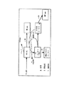
【0042】
この応用に用いられる装置構成は、図3に示される。湿潤オゾン気相工程と表示される装置は、オゾン拡散器を浸漬するに十分な量の液体のみで満たされた石英容器を用いる。液体は、たとえば酢酸のような添加物を添加された脱イオン水である。液体は石英容器の上に置かれる。液体は80℃に加熱される。ウエハーは、浸漬しないように、直接液体界面の上に置かれる。オゾン拡散器は、溶融シリカから加工され、ソルビウス発生器は、酸素流量3l/minで操作される。実験の間ずっと、オゾンは石英タンクの中に直接バブリングされる(気泡が減少しないように)。密閉容器の中の液体を加熱し、さらに連続してオゾンをバブリングすることにより、周囲の湿潤なオゾンにウエハーを曝す。気相での実験において、作業温度は80℃で、脱イオン水は酢酸で酸性にされる(1/100体積比)。すべてにおいて、ウエハーは10分処理され、続いて脱イオン水中で10分濯がれる。
【0043】
洗浄効率は、SEM観察(0.6μmのVIA構造の上の)に基づいて評価される。比較のため、ウエハーは、45分間酸素プラズマ処理され、乾式除去される(ウエハー上の側壁のポリマーを除く)。
【0044】
図4は、洗浄処理前(すなわち、レジストも側壁のポリマーも残っている状態)のVIA構造(図1)のSEM写真を示す。図5は、図1のVIA構造を45分間酸素でドライストリップ(dry strip)した時のSEM写真を示す。図1と図2の構造を10分間酢酸を添加し最適化された湿潤なオゾン気相プロセスに曝した後のSEM写真をそれぞれ図6と図7に示す。
【0045】
45分間の酸素によるドライストリップ処理後、側壁のポリマーがまだはっきりと見えることがわかる。しかし、気相処理に関しては、すばらしい洗浄効率が認められた(図6及び7)。気相処理においては、エッチング後の側壁のポリマーだけでなく、レジストコーティングも、表面には認められなかった。
酢酸添加による湿潤オゾン気相処理は、VIAエッチング構造からレジスト層及び側壁のポリマー残留物を除くのに有効であることが示された。これは、有機汚染物に対するオゾンによる除去効率が、物理的及び化学的に促進されたためである。
【0046】
<応用2:レジスト除去>
上述の様に、酢酸のような薬品添加物は、オゾン処理の化学的作用により有機汚染物の除去効率に影響を与える。この目的のために、レジスト層でコートされたウエハーは、いろいろなオゾン処理された脱イオン水混合物に曝される。レジスト除去効率が評価される。ウエハーはポジ(JSR電子製IX500el)及びネガ(Shipley製UVNF)レジストでコートされる。レジストで覆われたウエハーは、使用前にレジストを硬くするため、DUVによる焼き付け処理を行う。ポジレジストを備え、イオン注入されたウエハー(5e13at/cm2 P)が処理される。レジストの厚さは処理前後にエリプソメトリーによりモニターされる。
【0047】
気泡試験と表示され、別の特殊な応用に用いられるオゾンの比較用装置構成(浸漬型)は、図8に示され、7lの液体を入れる石英容器とタンクの底に位置するオゾン拡散器とからなる。液体は加熱される。作業温度は、45℃である。オゾン拡散器は溶融シリカから加工され、ソルビウス発生器は酸素流量3l/minで操作される。処理の間ずっと、オゾンは石英タンクの中(気泡が減少しないように)に、直接バブリングされる。ウエハーはオゾン拡散器の上に直接置かれ、液体の中に浸漬される。そのようにして、酸素/オゾンの気泡が表面と接触する。ウエハーは、図7に示される気泡セットアップにおいて、酢酸濃度を変化させながら、オゾン処理を受ける。イオン注入されていないウエハーは、脱イオン水7lに次の量の酢酸を加えた液、0、0.1ml(0.46mmol/l)、1.0ml(2.3mmol/l)及び5.0ml(11.5mmol/l)を用いてオゾン洗浄される。イオン注入されたウエハーは、0又は11.5mmol/lのいずれかの液を用いて、オゾン洗浄される。
【0048】
イオン注入されたレジストの場合、決められた量の酢酸を添加することにより、除去効率が約50%(60nm/min対90nm/min)増加する。イオン注入されたレジストの結果は、図9に示す。処理の効率数は次のように定義される。すなわち、オゾン濃度に対して規格化されたレジスト除去効率であり、単位処理時間当たりの除去速度で表わされる。上記のように定義された処理効率数は、ネガレジストでは0.8から1.2nm/(min*ppm)、ポジレジストでは4.5から8.5nm/(min*ppm)までである。ポジ及びネガレジストの除去の強度の違いの順序にも拘わらず、全体の傾向は同じである。処理効率数に対する明確な効果は、酢酸を添加した時に現われる。
【0049】
<応用3:レジスト除去>
上記に基づき、実験計画法を適用した。検討した効果は、オゾン処理した物質による、薬品添加物を用いた時のレジスト除去効率である。焼き付けたポジ及びネガレジストを試験に用いた。気泡試験と表示され、図8に示されたオゾンの比較用装置構成(浸漬型)を用いた。評価における個々の変数の影響をより明確にするため、ウエハーは直接オゾンの気泡に接触させなかった。この低いオゾンの利用性(気泡又は気体が接触しない)は、応用2と比べて低い除去速度と低い処理効率に反映される。考慮した変数は、温度や溶液のpHだけでなく、酢酸、過酸化水素及びオゾン(酸素流量を変えることにより)濃度である。pHの影響(硝酸を加えることにより、2から5まで変化させた)は、酢酸の効果がpHによるものであるかどうかを調べるために、検討に加えた。過酸化水素は、OHラジカルを発生させることが知られており、添加した。添加量は、0、0.1、又は0.2ml(英国アッシュランド製、30%)である。酢酸(ベーカー製試薬用、99%)の添加量は、脱イオン水7lに0、0.5又は1mlである。温度は、21から40℃の範囲で変え、オゾン濃度は発生器を通す酸素流量でコントロールした。低い流量は、3l/min、高い流量は5l/minである。ポジ及びネガレジストのいずれの除去においても、結果は、単位時間当たりのレジスト除去速度で表わされる。設定された実験条件と結果を表1に示す。RS/ディスカバー(Discover)が、実験結果の解析のために用いられる。これは、最小自乗法と二次モデルに基づき、段階的多重回帰法を用いて行われる。このモデルは、実験結果を90%の偏差で説明できる。
【0050】
【表1】

ポジレジストの結果のみを、図10と図11に示すが、ネガレジスト除去の統計量も同様である。すべての応答に対する主たる効果は図10に示す。レジスト除去に対する最大の明確な効果は、酢酸濃度の変化(0から715μl添加する)によるものであり、pHにはほとんど関係しないことに注意する必要がある。また、レジストの除去速度は、過酸化水素の添加(0から200μl)により減少する。このグラフから温度はあまり重要でないと結論できる。しかし、オゾン濃度は、温度に強く依存し(溶解度と安定性は、温度に反比例する)、片寄った結果を与える。そこで、処理効率数が定義される。すなわち、オゾン濃度に対して規格化されたレジスト除去効率であり、単位オゾン及び単位時間当たりの除去速度で表わされる(すなわち、nm/(min*ppm))。以上のように得られた処理効率数は、ポジレジストで0.2と4nm(min*ppm)の間、ネガレジストで0.03から0.4nm/(min*ppm)の間で変化する。ポジレジストの除去における処理効率数に対するいくつかのパラメータの影響の結果を図11に示す。ポジとネガレジスト除去の間の強度の差の順序にも拘わらず、全体の傾向は同じである。酢酸の添加、オゾン濃度及び温度の上昇が、処理効率数に明らかな効果を与える。
【0052】
<応用4:レジスト除去>
本発明の方法のさらなる検討において、他の試験について以下に述べる。
オゾン処理した物質に対する大きな要求は、有機汚染物(クリーンルームの空気成分、フォトレジスト又は側壁のポリマー)を速くかつ完全に除去することである。除去効率に大きな影響を与えるパラメータを確認されなくてはならない。酢酸添加は、結果に影響を与えるが、またオゾン濃度や温度などの他のパラメータも重要であることが、明らかにされた。そこで、ポジレジストの除去効率に対するオゾン濃度及び作業温度の影響が、実験的に評価された。5nmの厚さのフォトレジストでコーティングしたウエハーを準備し、脱イオン水を含む静的な浴に浸漬した(図8における装置構成、しかし浸漬の間はバブリングを中止する)。オゾン濃度は、0から12ppm、温度は20、45そして70℃の間で変化させた。故意に、静的状態で(すなわち、オゾンを脱イオン水に飽和させた後、気体を流すのを止める)、1分洗浄し、パラメータの影響を調べる。主な結果を図12に示す。洗浄効率をオゾン濃度に対して、3つの異なる温度範囲において、プロットした。短い処理時間と静的条件(オゾンの利用が限定される)のため、除去は50%程度である。オゾン濃度当たりの除去効率は、温度を高くすると向上するが、検討した時間内における全除去量は、オゾン濃度を高くすると向上することがわかる。しかし、オゾンの溶解度は、温度とともに減少するが、処理効果は温度とともに向上する。
【0053】
溶液におけるオゾン濃度、酸化力及び洗浄効果は、物理的状態に応じて最大にすることができる。米国特許第5464480号公報に開示された1つのプロセスは、オゾンの溶解度を増加させるため、温度を下げて(冷蔵して)、水を処理している。この方法の不利な点は、反応性が低下し、反応速度が遅いため、処理時間が長くなる点である。オゾン濃度を高くする他の可能性としては、より効率の良い、オゾン発生器及び/又はオゾンを脱イオン水に移行させるオゾン拡散器を使うことである。しかし、上記の結果から、すべての効率化されたプロセスは、作業温度において、オゾン濃度を最大にすることを目指すべきである。この仮説を、図2及び図8の装置において、実際に示す。ここでは、気泡接触(下方の周囲、高い温度で)を備えた従来の浸漬と湿潤な気相プロセス(高い温度で)とが示されている。両方の装置構成については、上述されている。ポジレジストのウエハー(1.2nm)が10分間、いろいろな温度で(気泡)、又は80℃(気相)で処理に曝される。結果を図13に示す。気泡実験の溶解オゾン濃度(棒グラフ)と洗浄効率(線グラフとクロス)を示す。気泡実験の挙動に関しては、低温域では速度要因に規制され、また高温域ではオゾンの溶解度により規制されていることが理解できる。後者による規制を、周囲に湿潤なオゾンを存在させる実験により、緩和させることができる。ウエハーを湿潤な雰囲気に曝すことにより、ウエハー上に薄い縮合層が形成される。周囲のオゾン気体は、連続して大量のオゾンを供給する(気体中では重量%、溶液中ではppm)。
また、薄い縮合層は拡散律速を減少させ、寿命の短い反応性の高いオゾン成分がウエハー表面に到達し易くし、100%近い除去率をもたらす。重要なことは、湿潤でない気相プロセスでは、うまくいかないということである。
【0054】
〈応用5:一連の洗浄における第1の工程〉
本発明の他の応用は、オゾンと蒸留水とからなる混合物のシリコンに対する酸化力を用いたものである。従来、シリコンウエハーの洗浄は以下の連続した工程で行われていた。
工程1:シリコン表面に酸化物を成長させる。
工程2:酸化物を除去する。
工程3(必要に応じて):親水的な表面が望ましい場合に、薄い絶縁酸化物層を成長させる。
工程4:シリコンウエハーを乾燥させる。
このような連続した工程に関する詳細は、「New Wet CleaningStrategies for obtaining highly Reliable Thin Oxides],M.Heyns et al,Mat.Res.Soc.Symp.Proc.Vol.315,p.35(1993)に説明されている。他の刊行物にも、上記のような連続した工程によれば、高い除去効率が得られ、かつ金属の混入が低レベルであることが示されている。
【0055】
以下に示す上記と異なる連続した工程を行うことができる。
工程1:オゾンと水との混合物流体(液体又は気体)のシリコン酸化力を用いて、シリコン表面に酸化物を成長させる。流体は、さらに捕捉剤のような添加物を含む。
工程2:単独又は塩酸等の添加物を含む希釈されたフッ酸洗浄剤中で酸化物を除去する。
工程3(必要に応じて):親水的な表面が望ましい場合、希塩酸/オゾン混合物又はオゾンと水の混合物のようなオゾン化された混合物中で、薄い絶縁酸化物層を成長させる。
工程4:マラゴンニ型の乾燥又はシリコンウエハーの加熱を伴う乾燥工程によりシリコンウエハーを乾燥させる。
この連続した工程は、ウエットベンチ、シングルタンク、スプレープロセッサー又はシングル‐ウエハークリーニングツール等の反応容器又はタンクにおいて行うことができる。
【0056】
〈オゾンの化学的性質に関する考察〉
水溶液にオゾンを含む本発明を用いて得られた結果に関する、別の考えられる機構について説明する。水溶液におけるオゾンの分解は、塩基により触媒され、ラジカル(A)又はイオン的(B)な開始機構に従う。
(A) O3+OH*-----→O2 -+*HO2 (1)
*HO2-----→H++*O2 - (2)
(B) O3+OH---→HO2 -+O2 (3)
H2O2-----→HO2 -+O2 (4)
O3+HO2 -------→*OH+*O2 -+O2 (5)
【0057】
さらに、オゾンの分解は、開始反応のタイプには関係なく、反応(6)と(7)を伴う。開始機構がイオン的であるかラジカル的であるかに拘わらず、少なくとも、単位水酸化物イオン当たり3個のオゾン分子が分解することが理解される。
O3+*O2--------→*O3 -+O2 (6)
*O3 -+H2O-----→*OH+OH+O2 (7)
【0058】
上記のオゾン分解経路に加え、OHラジカル(反応(5)と(7)で形成される)が、反応経路(8)によりさらにオゾンを分解させる。また、反応生成物が反応(2)、(6)及び(7)と結び付くことにより、連鎖反応が開始される。
*OH+O3----→*HO2+O2 (8)
【0059】
これらの分解機構は、中性又は塩基性の水性環境でのオゾンの消耗の説明に良いモデルである。しかし、酸性の場合、認められるオゾンの分解速度は、反応(1-4)において、水酸化物濃度から予想されるものより速くなる。したがって、別の分解機構が必要である。この開始機構は、既に述べた反応(2)、(6)及び(7)と組み合わせて、反応式(9-11)に示される。
O3----→O+O2 (9)
O+H2O----→2*OH (10)
【0060】
反応(1-10)は、水性環境におけるオゾンの消耗を表わしている。しかし、酸化される化合物が存在すると、状況は複雑になるため、全体の概要を第14図に示す。オゾンの水溶液への移動は、溶解度により規制されるため、パージを行う時にオゾンの損失が生じる。1次反応は、酸化される溶質Mにより、オゾンが消費される。
【0061】
これらの反応において、水の過酸化水素への酸化も起きる(結果として、H2O2 ←--→HO2 -+H+の平衡が生じる)。この1次反応は、通常遅いため、オゾンは別の反応経路により分解し易い。たとえば、開始剤I(OH,HO2 -,---)とオゾンの反応により、1次ラジカル(*OH)が生成し、それは除去されるか、又はさらにオゾンと反応し、さらに多くのラジカルを生成するか又は溶質Mのさらなる酸化に関与する。反応(1-10)と第14図を検討すると、オゾンの化学的性質は化学的に制御可能である(すなわち、添加物の選択的な添加により)。
【0062】
上記の点から得られたオゾンに対する添加物の影響は、オーバーフロー浴における酸素/オゾンの気泡を減らすため、オゾン/水混合物がゴア(Gore)オゾンモジュール(膜を基材にしたミキサー)で調製されるオーバーフローの浴で示される。オーバーフロー浴の水の流量(20l/min)、オゾン発生器を通す酸素の流量(2l/min)及びオゾンモジュールにおける圧力(1バール)が、浴における可能なオゾンレベルを決定する。これらの変数は、ここに記載された実験においては、所定の値で一定の保たれる。脱イオン水中のオゾンレベルは、薬品を添加する前、飽和の状態に常に保たれる。用いられるすべての薬品は、ベーカー製の試薬用酢酸(99%)を除いて、英国アッシュランド製である。反応速度の影響を減らすため、すべての実験は室温で行った。オービスフィア-ラボMOCA製電気化学式オゾンセンサーをオゾンの測定に用いた。
【0063】
第15図に示すように、オーバーフローさせたタンクの中の脱イオン水中のオゾン濃度に対する酢酸の挙動は、オゾンを飽和レベルにした後、酢酸(99%)10mlを脱イオン水に添加,することにより、検討されている。非常に速やかにオゾンレベルは、増加し始める。
【0064】
〈オゾン処理された物質のレジスト除去効率に対する酢酸の影響〉
間接的な酸化プロセスは、オゾン分解における連鎖を生長させるOHラジカルの存在に依存する(K.Sehested,H.Corfitzen,J.Holcman,J.Phys.Chem.,1992,96,1005−9)。G.AlderとR.Hill(J.Am.Chem.Soc.1950,72,1984)によれば、OHラジカルが有機物の分解に主な原因である。排水処理プロセスに通常用いられる方法には、紫外線照射、pH又は過酸化水素の添加がある。そのようにして、OHラジカルを生成させている。
【0065】
3つの異なる実験を行った。すなわち、まず、過酸化水素、次に酢酸に過酸化水素を添加する、最後に酢酸のみを添加する実験である。
【0066】
オゾン処理した脱イオン水に過酸化水素を添加した場合の、シリコンウエハーからのポジレジストの除去効率への影響を表2に示した。添加される過酸化水素の濃度は、脱イオン水中の実際のオゾン濃度のオーダーである。50μl(英国アッシュランド製、30%)のH2O2を7.5lタンクに添加した時は(0.08mmol/l)、大きな影響が認められた。測定されたレジスト除去速度は、4分の1近くに減少した。さらにH2O2を添加すると、レジスト除去効率はより低下し、ついには実質的に処理ができなくなる(2nm/minの除去速度)。これは、OHラジカルの量を増やすと、有機汚染物の除去速度が向上するという排水処理の場合とは、逆の結果である。排水処理において除去すべき有機物は、溶液の中に分散している。一方、我々の目的のためには、有機汚染物は、少なくとも半導体基板の1部を覆うような層の中に拘束されている必要がある。我々の目的にとっては、溶液の中の利用可能なオゾン及びオゾンによりもたらされる化合物の全体の量が問題なのではなく、むしろウエハー表面の近傍の有機物が拘束された層付近で発現する化学的活性が重要である。
【0067】
【表2】
したがって、この応用においては、OHラジカルにより触媒されるオゾンの分解機構は、形成されるOHラジカルの除去によりコントロールされる。捕捉剤は、他の成分による望ましくない影響を除くため、混合物又は他の系に添加される物質である。酢酸又は酢酸塩が、水性オゾン溶液の安定化剤である。第16図に、オゾン濃度に対する、酢酸及び過酸化水素の繰り返し添加(OHラジカルの生成促進)の協同効果を示す。時間t=0における添加(0.17mmol/l)にも拘わらず、脱イオン水が0.23mmol/lの酢酸のみで安定化されている場合、オゾン濃度はわずかに増加する。H2O2を数回添加した(それぞれ0.17mmol/l)後でも、オゾンレベルは最初のスタート時のレベルより低下しない。このことから、酢酸が、OHラジカルで開始されるオゾンの連鎖分解を止めるのに、大きな効果を持つことがわかる。
【0069】
少量の酢酸が添加された時の、オゾン処理した脱イオン水で10分間レジスト除去した時の実験結果を表3に示す、レジスト除去は処理時間10分として再計算され、除去速度(nm/min)で示されている。実験装置の問題で、測定されたオゾン濃度が全く定性的(オゾンセンサーと酸素/オゾン流の距離に再現性がない)であるということに注意する必要がある。0.02mmol/lから0.24mmol/lの酢酸をオゾン処理した脱イオン水に添加すると、添加しない比較プロセスと比べ50%程度レジスト除去効率が向上する。酢酸及び過酸化水素添加の協同効果をレジスト除去プロセスのために評価するとともに、表4に示す。これらの試験において、オゾン飽和後、脱イオン水は、まず、0.02mmol/lの酢酸を添加され、濃度の異なる過酸化水素が添加され、レジスト除去効率に対する効果が評価される。酢酸が存在している時、過酸化水素を添加すると、表2の効果と比べると弱いものではあるが、レジスト除去速度は低下する。また、酢酸を添加して得られる安定化効果は、溶液を酸性にした時の場合よりも強い(表2、硝酸を用いて)。
【0070】
【表3】
【表4】
酢酸を添加することにより、脱イオン水中のオゾン濃度を高くすることができる。しかし、レジスト除去効率の向上は、酢酸添加によるオゾン濃度の増加のみによっては説明できない。図9に、レジスト除去処理効率数に対する酢酸添加の影響を示すが、それはオゾン濃度に対して規格化されている。処理効率は、酢酸添加とともに、増加していることがわかる。したがって、未知の機構が関与していると考えられる。
【0073】
【発明の効果】
有機物は、廃水処理の場合のように均一に溶液の中に分散しているのではなく、シリコン表面の層の中に閉じ込められている。溶解しているオゾン(t1/2=20min)と反応性の高いオゾン種の短い寿命を考えると、廃水処理におけるオゾンの知識は、我々の応用には適用することはできない。有機物を確実に除去するためには、ウエハー近傍の有機物の拘束された層の付近で十分な化学的活性(反応性の高いオゾンを利用できること)が必要である。シリコンウエハー上の有機物の除去効率は、温度、オゾン濃度及び酢酸の添加に非常に影響される。温度とオゾン濃度の必要条件は、上記の湿潤なオゾン気体相の実験条件を満たしている。ウエハーを湿潤な雰囲気に曝すことにより、ウエハー表面に薄い縮合層が形成される。周囲のオゾン気体相により、薄い縮合層を通してシリコン表面の有機汚染物に向けて連続してオゾンが供給される。また、気泡実験において、気泡を含むオゾンが有機汚染物の拘束された層に常に接触している。
【0074】
酸化された酢酸溶液でOHラジカルが除去されると、以下に示す反応によりH2O2が生成する。
*OH+CH3COOH-----→*CH2COOH+H2O (11)
*CH2COOH+O2-----→*OOCH2COOH (12)
2*OOCH2COOH -----→0.7H2O2+Products (13)
反応(13)で形成される他の生成物には、ホルムアルデヒド、グリオキシル酸、グリコール酸及び有機過酸化物がある。
【0075】
酢酸フリーラジカル(反応(11))とレジスト表面との反応は、レジスト表面をオゾンと反応し易くするかもしれない。この反応は、水素原子の引き抜き反応を含み、不飽和結合を形成させる。この不飽和結合は、分子状オゾンと反応する。2番目に、レジスト表面に非常に近いところでフリーのOHラジカルを除去する。その結果、反応(11-13)により、たとえばH2O2が生成する。そして今度は、H2O2がレジスト表面の非常に近くに、コントロールされ局在化した”より強力な酸化力”(OHラジカル)を生成させる。
【図面の簡単な説明】
【図1】 深いVIAエッチ構造を示す概略図である。
【図2】 過度にAlエッチングされたVIA構造を示す概略図である。
【図3】 気相プロセスにおいて用いられる装置構成を示す図である。
【図4】 洗浄処理前のVIA構造を示すSEM写真である。
【図5】 45分間O2ドライストリップ後のVIA構造を示すSEM写真である。
【図6】 本発明の好ましい実施形態の方法に10分間曝した図1の深いVIA構造を示すSEM写真である。
【図7】 本発明の好ましい実施形態の方法に10分間曝した図2の過度にAlエッチングされたVIA構造のSEM写真である。
【図8】 液相プロセスにおいて用いられる装置構成を示す図である。
【図9】 酢酸濃度とポジ及びネガレジストの除去におけるレジスト除去工程の効率数の関係を示すグラフである。
【図10】 主たるパラメータのポジレジスト除去速度に対する影響を示すグラフである。
【図11】 主たるパラメータのポジレジスト除去工程の効率数への影響を示すグラフである。
【図12】 静的システムにおける温度とオゾン濃度とレジスト除去効率との関係を示すグラフである。
【図13】 気泡又は湿潤気相工程における温度とオゾン濃度とレジスト除去効率との関係を示すグラフである。
【図14】 水性オゾンにおける可能な反応式を示す。
【図15】 オーバーフロータンクにおけるOHラジカル捕捉のオゾン濃度に対する影響を示すグラフである。
【図16】 酢酸添加した脱イオン水に、繰り返し過酸化水素を添加した時の影響を示すグラフである。[0001]
BACKGROUND OF THE INVENTION
The present invention relates to a method for removing organic contaminants from the surface of a semiconductor substrate. The present invention further relates to the use of the method of the present invention for many applications such as multiple consecutive cleaning processes, or cleaning after VIA etching or other etching processes.
[0002]
[Prior art]
The preparation of the semiconductor substrate surface prior to various process steps such as oxidation, deposition or growth processes has become one of the most important problems in semiconductor technology. With the rapid spread of design rules below 0.5 microns and 0.25 microns, fine particles and low levels of contamination or impurities (~ 10Tenatoms / cm2, And less) have a significant impact on process yield. Contaminants to be removed from the semiconductor substrate surface include metal impurities, particles and organic matter. A commonly used method for reducing the contamination level of foreign matter on the surface of a semiconductor substrate is a method of immersing a wafer in a chemical solution.
[0003]
Organic matter is one of the contaminants that must be removed from the surface of a semiconductor wafer. In the pre-cleaning step, the absorbed organic molecules prevent contact between the wafer surface and the cleaning chemical, causing non-uniform etching and non-uniform cleaning of the wafer surface. In order to achieve a clean wafer surface, organic impurities must be removed prior to other wafer cleaning processes. Conventional wet cleaning processes involve the use of a sulfuric peroxide mixture (SPM) to remove organics. However, SPM uses expensive chemicals and needs to be used at high temperatures and causes chemical waste disposal problems.
[0004]
Other sources of organic contamination also occur in standard IC process flows. Examples thereof are a deposited photoresist layer or fluorocarbon polymer residue on a semiconductor substrate. A fluorocarbon polymer residue is formed when a semiconductor (silicon) semiconductor substrate is subjected to a dry oxide etching process. In an oxide etch using a normal fluorocarbon gas, a polymer is intentionally generated to increase the etch selectivity to the vertical sidewall profile and the photoresist mask and underlying film. SiO2Etch selectivity in Si systems is achieved at specific process conditions through the production of fluorocarbon-based polymers. The polymerization reaction tends to occur on Si, forms a protective film, and Si and SiO2Provides etch selectivity between. After selective etching, the resist and polymeric residue need to be removed from the surface. If the polymer is not completely removed before the next metal deposition, the polymer mixes with sputtered metal atoms and forms a high resistance material that affects reliability. The method of polymer removal depends on the plasma etch chemistry, the plasma source and the composition of the deposited film. However, in dry processes, gases containing O2 or H2 have been used to remove fluorocarbon polymers. In wet cleaning techniques, amine-based solvents (US Pat. No. 5,279,771 and US Pat. No. 5,308,745) are often used. The removal of organic photoresist usually involves wet or dry oxidative chemical action (ie, O2Dissolution processes based on plasma, SPM) or solvent stripping are included. These processes are expensive and are environmentally harmful with respect to waste disposal.
[0005]
[Problems to be solved by the invention]
In the process of finding other effective cleaning methods for removing organic contaminants (photoresist and etching residues) from the Si surface, the use of ozone treatment chemistry was investigated. Ozone is widely used in the fields of wastewater treatment and drinking water sterilization due to its strong oxidizing power. A further advantage of ozone is that the residue after decomposition and / or reaction (H2O, CO2, O2) Is harmless. Oxidation of ozone to organic pollutants is generally considered to involve two different oxidation pathways, direct oxidation or indirect oxidation. Direct oxidation or ozonolysis involves molecular ozone as the first oxidant. It first occurs at a carbon-carbon double bond. This type of oxidation is likely to occur when the wastewater is in the low pH range. Indirect oxidation involves a second oxidant, such as a first oxidant (eg, OH radicals). This type of oxidation is more reactive but less sensitive and is prone to the generation of OH radicals, high pH, high temperature, accelerators (eg, H2O2) And ultraviolet irradiation. In actual situations, a mixture of contaminants having different reactivities to ozone is often the subject of treatment. However, in order for both oxidation pathways to occur simultaneously and indirect oxidation to proceed, it is necessary to sacrifice the removal efficiency of organic contaminants that are highly reactive with molecular ozone. In order to optimize the removal efficiency of organic matter by the chemical action of ozone treatment, it is important to identify parameters that affect both oxidation pathways.
[0006]
In recent years, ozone has been introduced into the microelectronics industry due to its strong oxidizing power. When ozone is dissolved in water, its autolysis time is faster than in the gas phase. During autolysis, ozone generates OH radicals as a reaction byproduct. G. Alder and R.W. Hill (J. Am. Chem. Soc. 1950, 72 (1984))) is believed to be due to the decomposition of organic matter.
[0007]
US Pat. No. 5,464,480 discloses a method for removing organic matter from a semiconductor wafer. The wafer is brought into contact with an aqueous solution containing ozone in the temperature range of 1 ° C. to 15 ° C. The wafer is placed in a tank containing deionized water. The ozone is then diffused into deionized water at room temperature or lower for a time sufficient to remove organics from the wafer. Meanwhile, the temperature of the deionized water is kept between 1 ° C and 15 ° C. Next, rinse the wafer with deionized water. The reason why the temperature of the solution is kept between 1 ° C. and 15 ° C. is that a sufficiently high concentration of ozone needs to be present in the water in order to oxidize all organic substances on the wafer into an insoluble gas. is there.
[0008]
European patent application EP-A-0548596 discloses a semiconductor substrate in a cleaning chamber filled with various liquid chemicals, ultrapure water, or a mixed phase fluid composed of ozone-containing gas and ultrapure water in a treatment chamber filled with ozone gas. Alternatively, a spray tool process is disclosed that sprays onto a semiconductor wafer. It is necessary to rotate the film in order to always refresh the thin film of the treatment liquid and to promote removal of undesirable substances by centrifugal force.
[0009]
US Pat. No. 5,181,985 discloses a semiconductor wafer surface treatment process using chemicals in a wet process. According to this, an aqueous phase containing one or more liquid chemically active substances reacts on the wafer surface in the form of a finely divided liquid like mist. The process consists of spraying mist water on the wafer surface and interacting with the gas phase and liquid phase on the semiconductor wafer surface, so that the gas is chemically active to bind to the mist water. A process of introducing a new substance. The chemically active substance is selected from the group consisting of gaseous ammonia, hydrogen chloride, hydrogen fluoride, ozone, ozonated oxygen, chlorine and bromine. Water with a temperature of 10 ° C. to 90 ° C. is introduced into the system.
[0010]
US Pat. No. 5,503,708 discloses a method and apparatus for removing organic films. That is, a mixed gas containing alcohol and one of ozone gas or ozone-containing gas is introduced into the processing chamber until at least the semiconductor wafer is placed in the processing chamber, and an organic film formed on the surface of the semiconductor wafer Allow the gas mixture to react.
[0011]
Japanese Patent Application Laid-Open No. 61-004232 discloses a method for cleaning a semiconductor substrate. The method was developed in the prior art as an alternative to the traditional acid-hydrogen peroxide cleaning used to reduce heavy metals on silicon wafers. The semiconductor substrate is immersed in a concentrated solution of organic acid such as formic acid or acetic acid filled in the cleaning tank, and ozone or oxygen is supplied from the bottom of the tank so as to stir the solution. The solution is heated so that the temperature is between 100 and 150 ° C. Organic waste is oxidized by ozone, dissolved and removed. In other words, this Japanese publication discloses a method of removing heavy metals in the form of metal formate and acetate and a method of removing organic waste from a semiconductor wafer by ozone.
[0012]
The present invention aims to propose an improved method for removing organic contaminants from a semiconductor semiconductor substrate. More specifically, an object of the present invention is to propose a method for removing organic contaminants such as photoresist, resist residue, dry etching residue, and the like that occur in any process related to semiconductor substrate fabrication from the surface of the semiconductor substrate. To do.
[0013]
[Means for Solving the Invention]
The first aspect of the present invention comprises a step of holding a semiconductor substrate in a tank and a step of filling the tank with a gas mixture comprising water vapor, ozone and an additive acting as a scavenger.
The term tank used in the context of the present invention and related patent applications means any kind of tool or reaction vessel that holds a substance for cleaning or removing organic contaminants. Therefore, the term “tank” includes the conventionally known wet benches, vessels, spray processors, spinning tools, single tanks, single wafer cleaning tools. Tools such as (single wafer cleaning tools) and reaction vessels are included.
The second aspect of the present invention includes a step of holding a semiconductor substrate in a tank, a step of filling the tank with a liquid composed of water, ozone and an additive acting as a scavenger, and a temperature of the liquid below its boiling point. The process of maintaining to.
The third aspect of the present invention comprises a step of holding a semiconductor substrate in a tank and a step of filling the tank with water, ozone, and an additive acting as a scavenger, and the liquid of the additive. The ratio in the inside is 1 mol% or less of the liquid.
[0014]
A scavenger means a substance added to any system, such as a mixture or liquid, gas, solution, etc., to prevent undesired effects by the mixture or other components of the system.
The additive preferably serves as an OH radical scavenger. A radical is an uncharged species (ie it is a one or two atom or polyatomic molecule) and has at least one unpaired electron. Examples of scavengers include acetic acid (CHThreeCOOH), acetate (CHThreeCOO-), Carbonate (HxCOThree -(2-x)), Phosphate (HThreePOFour -(3-x)) Or a carboxylic acid or a salt thereof.
[0015]
In the third embodiment of the present invention, a mixture of ozone and distilled water having the ability to oxidize silicon is used. The third embodiment relates to an efficient method for cleaning a silicon surface, and relates to the following continuous steps.
Step 1: Oxide is grown on the silicon surface.
Step 2: The oxide is removed.
Step 3 (optional): If a hydrophilic surface is desired, grow a thin insulating oxide layer.
Step 4: Dry the silicon wafer.
[0016]
The following continuous steps different from the above can also be used.
Step 1: Oxide growth on the silicon surface is performed using a fluid (liquid or gas) mixture of ozone and water capable of oxidizing silicon. The fluid may further include additives such as scavengers.
Step 2: The oxide is removed in a dilute hydrofluoric acid detergent containing or not containing hydrochloric acid or the like.
Step 3 (optional): If a hydrophilic surface is desired, a thin insulating oxide film is grown in an ozonated mixture such as a mixture of dilute hydrochloric acid and ozone.
Step 4: The silicon wafer is dried by Maragononi-type drying or drying accompanied by heating of the silicon wafer.
This continuous process can be performed using any reaction vessel or tank such as a wet bench, a single tank, a spray processor, a single wafer cleaning tool, and the like.
[0017]
The present invention can be used in the manufacture of silicon wafers for integrated circuits. The invention can also be used in related fields such as flat display, solar cell manufacturing or in micromachining applications or other fields where organic contaminants need to be removed from semiconductor substrate surfaces.
[0018]
DETAILED DESCRIPTION OF THE INVENTION
An object of the present invention relates to a method for removing organic contaminants from a semiconductor substrate surface.
The above method can be used to remove photoresist and etched organic residues from the silicon surface. The organic contaminant is a constrained layer that covers at least a portion of the semiconductor substrate. The thickness of the constrained layer ranges from a monomolecular layer or less to 1 μm. The above method can be applied to gas phase or liquid phase processes.
In the following description, a first preferred embodiment of the present invention directed to a gas phase process and a second preferred embodiment of the present invention directed to a liquid phase process are disclosed.
[0019]
<First Preferred Embodiment for Gas Phase Process>
In the gas phase process, the semiconductor substrate is placed in a tank so as to be in contact with a gas mixture containing water vapor, ozone and an additive that acts as a scavenger. A scavenger is a substance that is added to the mixture in order to eliminate unwanted effects from other components. The scavenger acts mainly as an OH radical scavenger. The additive is carboxylic acid or phosphoric acid or a salt thereof. More preferably, the additive is acetic acid.
[0020]
The proportion of the additive in the gas mixture is preferably 10 mol% or less of the gas mixture. The ratio of the additive in the gas mixture is more preferably 1 mol% or less of the gas mixture. Even more preferably, the proportion of additive in the gas mixture is not more than 0.5 mol% by weight of the gas mixture. Even more preferably, the proportion of additive in the gas mixture is not more than 0.1 mol% of the gas mixture.
[0021]
The gas mixture may include oxygen, nitrogen, argon or any other inert gas. The ozone concentration of the gas mixture is mainly 10-15 mol% or less. The water vapor is mainly saturated at the use temperature of the mixture. The use temperature of the mixture is 150 ° C. or lower, and is preferably higher than the temperature of the semiconductor substrate.
[0022]
A step of rinsing the semiconductor substrate with a solution may also be included. The solution used for rinsing is preferably composed of deionized water. The solution used for rinsing may further comprise hydrochloric acid and / or hydrofluoric acid, and / or nitric acid, and / or carbon dioxide, and / or ozone. Further, the solution used for rinsing may be subjected to megason ultrasonic stirring.
[0023]
Preferably, the present embodiment includes a step of filling the tank with at least water and a liquid composed of the additive, and the liquid is heated with the liquid level of the tank below the semiconductor substrate. The tank is then filled with saturated steam containing additives. The tank is further filled with ozone. Preferably, ozone is bubbled through the liquid. The liquid is preferably heated in the range of 16 ° C to 99 ° C, more preferably between 20 ° C and 90 ° C. Even more preferably, it is heated between 60 ° C and 80 ° C.
[0024]
In an apparatus configuration labeled as a wet ozone gas phase process, it is preferable to use a quartz container filled with only a small amount of liquid sufficient to completely immerse the ozone diffuser. The liquid is deionized water with an additive such as acetic acid added. The liquid is placed on a quartz container. The liquid is heated to 80 ° C. The wafer is placed so as not to immerse directly on the liquid interface. The ozone diffuser is assembled from fused silica, and the ozone generator (Sorbius) is operated with oxygen flowing to maximize the amount of ozone. Desirably, the oxygen flow rate is 3 l / min. Throughout the experiment, ozone is bubbled directly into the liquid (bubbles are not reduced). The wafer is exposed to wet ambient ozone by heating the liquid in a sealed container and continuously bubbling ozone through the liquid. In the gas phase experiment, the working temperature is 80 ° C. and the deionized water is acidified with acetic acid (1/100 volume ratio). The wafer is processed for a sufficiently long time, followed by a rinsing step after wet gas phase processing. In the experiment, the wafer is treated for 10 minutes and subsequently rinsed with deionized water for 10 minutes.
[0025]
Still further, it contains distilled water to which acetic acid has been added (
[0026]
Further, a 10 minute cleaning process including a combination of a continuous ozone vapor phase process at 80 ° C. for 10 minutes and an acid cleaning process at 90 ° C. for 10 minutes using a hydrogen peroxide solution containing 5% sulfuric acid is performed. Also good.
[0027]
<Second Preferred Embodiment for Liquid Phase Process>
In the liquid phase process, the semiconductor substrate is placed in a tank so as to come into contact with a liquid consisting of a mixture of water, ozone and an additive that acts as a scavenger. A scavenger is a substance that is added to a mixture in order to remove unwanted effects from other components. The scavenger mainly serves as a scavenger for OH radicals.
[0028]
The additive is carboxylic acid or phosphoric acid or a salt thereof, preferably acetic acid. The ratio of the additive in the liquid is 1 mol% or less of the liquid. Preferably, the proportion of additive in the liquid is 0.5 mol% or less of the liquid. More preferably, the ratio of the additive in the liquid is 0.1 mol% or less of the liquid. The liquid is further stirred megasonically.
[0029]
Preferably, the method further includes the step of maintaining the liquid at a temperature below its boiling point. The temperature of the liquid is preferably 100 ° C. or lower. More preferably, it is between 16 ° C and 99 ° C. More preferably, it is between 20 ° C and 90 ° C. More preferably, it is between 60 ° C and 80 ° C.
[0030]
The ozone is preferably bubbled through the liquid so that the bubbles of ozone are in contact with the semiconductor substrate.
[0031]
More preferably, the method further includes a step of rinsing the semiconductor substrate with a solution. The solution used for rinsing is preferably composed of deionized water. More preferably, the solution used for rinsing further contains hydrochloric acid and / or hydrofluoric acid, and / or nitric acid, and / or carbon dioxide, and / or ozone. The solution used for rinsing is stirred by megason sonication.
[0032]
In the present embodiment, the following apparatus configuration is preferably used. The ozone device configuration (immersion type) displayed as a bubble test consists of a quartz container containing 7 l of liquid and an ozone diffuser located at the bottom of the tank. The liquid is heated. The working temperature is 45 ° C. The ozone diffuser is fabricated from fused silica and the oxygen generator is adjusted so that the ozone generator (Sorbius) maximizes the amount of ozone in the gas flow. Most preferably, an oxygen flow rate of 3 l / min is used. Throughout the experiment, ozone is bubbled directly into the quartz tank (without depletion). The semiconductor substrate is placed directly on the ozone diffuser and immersed in the liquid.
[0033]
Oxygen / ozone bubbles come into contact with the surface. The semiconductor substrate is subjected to ozone treatment by changing the acetic acid concentration in the bubble device. The semiconductor substrate was added to 7 l of deionized water and the acetic acid concentration was 0 to 11, 5 mol / l (0, 0.1 ml (0.46 mmol / l), 1.0 ml (2.3 mol / l), and 5. Ozone cleaning is performed with the liquid changed in the range of 0 ml (11.5 mmol / l).
[0034]
More preferably, a conventional reaction vessel can be used for bringing the water containing the scavenger and the gaseous chemically active substance into contact with the surface of the semiconductor wafer. Examples of such reaction vessels include F.I. S. Those sold by companies such as I, SEMITOOL and STEAG can be used. When using such a reaction vessel, one or a plurality of semiconductor wafers are inserted into a predetermined position. The supply of finely separated water and / or gaseous chemically active substances and their uniform action on the wafer surface can be controlled. The water produced in the process is collected and then removed. After the processing, the wafer can be easily taken out, and a wafer to be processed next is inserted if necessary.
[0035]
It is also possible to provide means for swinging the wafer at a predetermined position, for example, by rotation. A conventional wet bench, or a reaction vessel made similar to or based on a spray etching or spray cleaning vessel or a spray processor can be used. Instead of means for introducing various solutions, means for supplying various gases and water are preferably used. It is basically possible to use a mixing system with means for introducing gas and liquid. It is also possible to spray water into the reaction vessel using a nozzle device that can spray a uniform, aerosol-like mist into the vessel. The fog consists of finely dispersed droplets. It is also possible to fill the reaction vessel with a gaseous atmosphere containing ozone and to spray the treatment liquid onto an undesirable substance on the semiconductor substrate rotating in the reaction vessel.
[0036]
Examples of the treatment liquid used in this embodiment include a liquid chemical substance, ultrapure water containing a scavenger, and a mixed phase liquid of ozone-containing gas and ultrapure water.
[0037]
As an apparatus for processing a semiconductor substrate, a hermetically sealed processing container having a semiconductor substrate holder for fixing a plurality of semiconductor substrates therein can be cited. The semiconductor substrate holder is coupled to a processing vessel coupled with a rotating shaft or a rotating table connected to the rotating shaft, and supplies a mixed phase fluid consisting of a nozzle for supplying ozone-containing gas or processing liquid or ozone-containing gas and processing liquid. A nozzle is provided.
[0038]
More specifically, various liquid chemicals, ultrapure water and scavengers, or mixed phase fluids containing ozone-containing gas and ultrapure water and scavengers are deposited on undesired substances on a semiconductor substrate in a processing vessel. Spray on. Here, an ozone-containing gas or a mixed phase fluid composed of ozone-containing gas and ultrapure water is supplied to the processing container, and the ozone concentration is adjusted to be kept at a predetermined concentration or a high concentration. When spraying, by rotating the semiconductor substrate on which the undesired substance is present on the surface, the thin film of the treatment liquid on the semiconductor substrate is constantly updated by centrifugal force, and the removal of the undesired substance is promoted. The effect increases when the semiconductor substrate is rotated at high speed. This is because the ultrapure water film on the semiconductor substrate is very thin and is continuously removed. Heating the liquid is also very effective.
[0039]
【Example】
The present invention can also be used in the applications described below with the methods disclosed in the two preferred forms of the present invention.
<Application 1: VIA cleaning>
The method of the present invention can be used for a wafer cleaning technique in the submicron process after the plasma etching process. Dry etching of silicon and its compounds is based on reaction with fluorine, resulting in contamination with fluorocarbon polymers. The fluorocarbon residue is generated when the semiconductor (silicon) semiconductor substrate is subjected to dry oxide etching. In a conventional oxide etch using a fluorocarbon gas, a polymer is intentionally generated to create a vertical sidewall profile and to increase etch selectivity to the photoresist mask and underlying film. SiO2Etch selectivity in the -Si system is achieved under certain conditions through the production of fluorocarbon-based polymers.
[0040]
The polymerization reaction preferably occurs on Si. By doing so, a protective layer is formed and Si and SiO are formed.2Etch selectivity between is achieved. After selective etching, the resist and polymeric residue must be removed from the surface. If the polymer is then not completely removed prior to metal lamination, the polymer will mix with the sputtered metal atoms, creating a high resistance material, causing problems that affect reliability. The polymer removal method depends on the chemical method of plasma etching, the plasma source, and the composition of the laminated film. However, in a dry process, a gas containing oxygen or hydrogen is used to remove the fluorocarbon polymer. In the wet cleaning method, amine-based solvents described in US Pat. No. 5,279,771 and US Pat. No. 5,308,745 are often used. These processes are largely expensive and are harmful to the environment with regard to waste disposal.
[0041]
1 and 2 show different VIA test structures prepared on a p-type wafer. The first structure consists of a 500 nm oxide layer, 30/80 nm Ti / TiN layer, 700 nm AlSiCu layer, 20/60 nm Ti / TiN, 250 nm oxide, 400 nm SOG, 500 nm oxide (silicon semiconductor Starting with the substrate). The second structure consists of the following layers of 500 nm oxide, 30/80 nm Ti / TiN, 700 nm AlSiCu, 20/60 nm Ti / TiN and 500 nm oxide (also starting from a silicon semiconductor substrate). . Subsequently, these structures are coated with an I-line resist and exposed through a mask set with contact holes with a diameter of 0.4 to 0.8 μm. The VIA structure is etched in a CF4 / CHF3 plasma. As the first step of the wafer, the VIA structure is etched through 500 nm oxide / 400 nm SOG / 250 nm oxide and stops on the TiTiN / Al layer. As a second step, the VIA structure is etched through the 500 nm oxide layer and into the TiTiN / Al layer. The wafer is directly ozone cleaned (leaving the resist layer and the polymer on the sidewalls on the wafer).
[0042]
The device configuration used for this application is shown in FIG. An apparatus labeled as a wet ozone gas phase process uses a quartz container filled with only a sufficient amount of liquid to immerse the ozone diffuser. The liquid is deionized water to which an additive such as acetic acid has been added. The liquid is placed on a quartz container. The liquid is heated to 80 ° C. The wafer is placed directly on the liquid interface so as not to immerse. The ozone diffuser is fabricated from fused silica and the sorbius generator is operated at an oxygen flow rate of 3 l / min. Throughout the experiment, ozone is bubbled directly into the quartz tank (so that bubbles are not reduced). The wafer is exposed to the surrounding moist ozone by heating the liquid in the sealed container and continuously bubbling ozone. In the gas phase experiment, the working temperature is 80 ° C. and deionized water is acidified with acetic acid (1/100 volume ratio). In all, the wafer is processed for 10 minutes followed by a 10 minute rinse in deionized water.
[0043]
The cleaning efficiency is evaluated based on SEM observations (over a 0.6 μm VIA structure). For comparison, the wafer is oxygen plasma treated for 45 minutes and dry removed (except for the sidewall polymer on the wafer).
[0044]
FIG. 4 shows an SEM photograph of the VIA structure (FIG. 1) before the cleaning process (ie, with both resist and sidewall polymer remaining). FIG. 5 shows an SEM photograph of the VIA structure of FIG. 1 when dry stripped with oxygen for 45 minutes. FIGS. 6 and 7 show SEM photographs after exposing the structures of FIGS. 1 and 2 to an optimized wet ozone gas phase process with acetic acid added for 10 minutes, respectively.
[0045]
It can be seen that the polymer on the sidewall is still clearly visible after 45 minutes of dry strip treatment with oxygen. However, excellent cleaning efficiency was observed for gas phase processing (FIGS. 6 and 7). In the vapor phase treatment, not only the polymer on the side wall after etching but also the resist coating was not observed on the surface.
Wet ozone gas phase treatment with acetic acid addition has been shown to be effective in removing resist layers and sidewall polymer residues from VIA etched structures. This is because the removal efficiency of organic pollutants by ozone is physically and chemically promoted.
[0046]
<Application 2: Resist removal>
As described above, chemical additives such as acetic acid affect the removal efficiency of organic contaminants by the chemical action of ozone treatment. For this purpose, a wafer coated with a resist layer is exposed to various ozone-treated deionized water mixtures. The resist removal efficiency is evaluated. The wafer is coated with positive (IX500el from JSR Electronics) and negative (UVNF from Shipley) resist. The wafer covered with the resist is baked by DUV in order to harden the resist before use. A wafer (5e13 at / cm 2 P) having a positive resist and ion-implanted is processed. The resist thickness is monitored by ellipsometry before and after processing.
[0047]
A device configuration for ozone comparison (immersion type) labeled as bubble test and used for another special application is shown in FIG. 8 and includes a quartz container containing 7 l of liquid and an ozone diffuser located at the bottom of the tank. Consists of. The liquid is heated. The working temperature is 45 ° C. The ozone diffuser is fabricated from fused silica and the sorbius generator is operated at an oxygen flow rate of 3 l / min. Throughout the process, ozone is bubbled directly into the quartz tank (so that bubbles are not reduced). The wafer is placed directly on the ozone diffuser and immersed in the liquid. As such, oxygen / ozone bubbles are in contact with the surface. The wafer undergoes ozone treatment while changing the acetic acid concentration in the bubble setup shown in FIG. Non-ion-implanted wafers were prepared by adding the following amount of acetic acid to 7 l of deionized water, 0, 0.1 ml (0.46 mmol / l), 1.0 ml (2.3 mmol / l), and 5.0 ml. Ozone cleaning with (11.5 mmol / l). The ion-implanted wafer is ozone cleaned using either 0 or 11.5 mmol / l solution.
[0048]
In the case of ion-implanted resist, the removal efficiency is increased by about 50% (60 nm / min vs. 90 nm / min) by adding a predetermined amount of acetic acid. The result of the ion-implanted resist is shown in FIG. The processing efficiency number is defined as follows. That is, the resist removal efficiency standardized with respect to the ozone concentration, which is represented by the removal rate per unit processing time. The processing efficiency numbers defined above are from 0.8 to 1.2 nm / (min * ppm) for negative resists and from 4.5 to 8.5 nm / (min * ppm) for positive resists. Regardless of the order of difference in the intensity of positive and negative resist removal, the overall trend is the same. A clear effect on the treatment efficiency number appears when acetic acid is added.
[0049]
<Application 3: Resist removal>
Based on the above, the experimental design was applied. The studied effect is the resist removal efficiency when chemical additives are used due to the ozone-treated substance. The baked positive and negative resists were used for the test. A device configuration for ozone comparison (immersion type) shown in FIG. 8 was used. In order to clarify the influence of individual variables in the evaluation, the wafer was not directly contacted with ozone bubbles. This low availability of ozone (no bubbles or gas contact) is reflected in a low removal rate and low processing efficiency compared to
[0050]
[Table 1]
Only the positive resist results are shown in FIGS. 10 and 11, but the negative resist removal statistics are similar. The main effect on all responses is shown in FIG. It should be noted that the greatest clear effect on resist removal is due to changes in acetic acid concentration (adding 0 to 715 μl) and has little to do with pH. Also, the resist removal rate decreases with the addition of hydrogen peroxide (0 to 200 μl). From this graph it can be concluded that temperature is not very important. However, ozone concentration is strongly dependent on temperature (solubility and stability are inversely proportional to temperature), giving an offset result. Therefore, the processing efficiency number is defined. That is, the resist removal efficiency normalized with respect to the ozone concentration, which is represented by the removal rate per unit ozone and unit time (that is, nm / (min * ppm)). The number of processing efficiencies obtained as described above varies between 0.2 and 4 nm (min * ppm) for positive resist and between 0.03 and 0.4 nm / (min * ppm) for negative resist. The results of the influence of several parameters on the processing efficiency number in positive resist removal are shown in FIG. Despite the order of intensity differences between positive and negative resist removal, the overall trend is the same. Addition of acetic acid, ozone concentration and temperature increase have a clear effect on the treatment efficiency number.
[0052]
<Application 4: Resist removal>
In further discussion of the method of the present invention, other tests are described below.
A major requirement for ozonated materials is fast and complete removal of organic contaminants (clean room air components, photoresists or sidewall polymers). Parameters that have a large impact on removal efficiency must be identified. It has been shown that acetic acid addition affects the results, but other parameters such as ozone concentration and temperature are also important. Thus, the effects of ozone concentration and working temperature on the positive resist removal efficiency were experimentally evaluated. A 5 nm thick photoresist coated wafer was prepared and immersed in a static bath containing deionized water (device configuration in FIG. 8, but bubbling was stopped during immersion). The ozone concentration was varied between 0 and 12 ppm and the temperature was varied between 20, 45 and 70 ° C. Intentionally, in a static state (ie, after saturating ozone with deionized water, stop the gas flow), wash for 1 minute and examine the effect of the parameters. The main results are shown in FIG. The cleaning efficiency was plotted against ozone concentration at three different temperature ranges. Removal is on the order of 50% due to short processing times and static conditions (with limited use of ozone). It can be seen that the removal efficiency per ozone concentration is improved when the temperature is increased, but the total removal amount within the examined time is improved when the ozone concentration is increased. However, the solubility of ozone decreases with temperature, but the treatment effect improves with temperature.
[0053]
The ozone concentration, oxidizing power and cleaning effect in the solution can be maximized depending on the physical state. One process disclosed in US Pat. No. 5,464,480 treats water at a reduced temperature (refrigerated) to increase the solubility of ozone. The disadvantage of this method is that the processing time is increased because the reactivity is lowered and the reaction rate is slow. Another possibility to increase the ozone concentration is to use a more efficient ozone generator and / or an ozone diffuser that transfers ozone to deionized water. However, from the above results, all streamlined processes should aim to maximize the ozone concentration at the working temperature. This hypothesis is actually demonstrated in the apparatus of FIGS. Here, conventional immersion with bubble contact (under ambient, at high temperature) and wet gas phase process (at high temperature) are shown. Both device configurations have been described above. A positive resist wafer (1.2 nm) is exposed to processing for 10 minutes at various temperatures (bubbles) or at 80 ° C. (gas phase). The results are shown in FIG. The dissolved ozone concentration (bar graph) and the cleaning efficiency (line graph and cross) of the bubble experiment are shown. Regarding the behavior of the bubble experiment, it can be understood that it is regulated by the speed factor in the low temperature region and by the solubility of ozone in the high temperature region. The latter restriction can be relaxed by experiments in the presence of moist ozone around. By exposing the wafer to a humid atmosphere, a thin condensation layer is formed on the wafer. The surrounding ozone gas continuously supplies a large amount of ozone (wt% in gas, ppm in solution).
In addition, the thin condensation layer reduces the diffusion rate control, makes it easy for highly reactive ozone components with a short lifetime to reach the wafer surface, resulting in a removal rate of nearly 100%. The important thing is that it does not work for gas phase processes that are not wet.
[0054]
<Application 5: First step in a series of cleaning>
Another application of the present invention is to use the oxidizing power for silicon of a mixture of ozone and distilled water. Conventionally, cleaning of a silicon wafer has been performed in the following continuous process.
Step 1: Oxide is grown on the silicon surface.
Step 2: The oxide is removed.
Step 3 (optional): If a hydrophilic surface is desired, a thin insulating oxide layer is grown.
Step 4: Dry the silicon wafer.
Details regarding such a continuous process are described in “New Wet Cleaning Strategies for Obtaining High Reliable Thin Oxides”, M. Heyns et al, Mat. Res. Soc. Proc. Vol. 315, p. Other publications also show that the continuous process as described above provides high removal efficiency and low levels of metal contamination.
[0055]
The following continuous steps different from the above can be performed.
Step 1: Oxide is grown on the silicon surface using the silicon oxidizing power of a fluid mixture (liquid or gas) of ozone and water. The fluid further includes additives such as scavengers.
Step 2: Oxide is removed either alone or in a diluted hydrofluoric acid detergent containing additives such as hydrochloric acid.
Step 3 (optional): If a hydrophilic surface is desired, grow a thin insulating oxide layer in an ozonated mixture such as dilute hydrochloric acid / ozone mixture or ozone and water mixture.
Step 4: The silicon wafer is dried by a Maragononi-type drying or a drying step involving heating of the silicon wafer.
This continuous process can be performed in a reaction vessel or tank such as a wet bench, a single tank, a spray processor or a single-wafer cleaning tool.
[0056]
<Consideration on chemical properties of ozone>
Another possible mechanism for the results obtained using the present invention with ozone in the aqueous solution is described. The decomposition of ozone in aqueous solution is catalyzed by a base and follows a radical (A) or ionic (B) initiation mechanism.
(A) OThree+ OH * ----- → O2 -+ * HO2 (1)
* HO2----- → H++ * O2 - (2)
(B) OThree+ OH --- → HO2 -+ O2 (3)
H2O2----- → HO2 -+ O2 (4)
OThree+ HO2 ------- → * OH + * O2 -+ O2 (5)
[0057]
Furthermore, the decomposition of ozone involves reactions (6) and (7) regardless of the type of initiation reaction. It is understood that at least three ozone molecules per unit hydroxide ion decompose, regardless of whether the initiation mechanism is ionic or radical.
OThree+ * O2-------- → * OThree -+ O2 (6)
* OThree -+ H2O ----- → * OH + OH + O2 (7)
[0058]
In addition to the ozonolysis pathway described above, OH radicals (formed by reactions (5) and (7)) further decompose ozone through the reaction pathway (8). Moreover, a chain reaction is started when a reaction product couple | bonds with reaction (2), (6) and (7).
* OH + OThree---- → * HO2+ O2 (8)
[0059]
These degradation mechanisms are good models for explaining ozone depletion in neutral or basic aqueous environments. However, when acidic, the observed ozone decomposition rate is faster in reaction (1-4) than expected from the hydroxide concentration. Therefore, another disassembly mechanism is necessary. This initiation mechanism is shown in the reaction formula (9-11) in combination with the reactions (2), (6) and (7) already described.
OThree---- → O + O2 (9)
O + H2O ---- → 2 * OH (10)
[0060]
Reaction (1-10) represents the depletion of ozone in an aqueous environment. However, the presence of a compound to be oxidized complicates the situation, and the overall outline is shown in FIG. Since the movement of ozone into the aqueous solution is regulated by the solubility, ozone loss occurs when purging. In the primary reaction, ozone is consumed by the solute M being oxidized.
[0061]
In these reactions, water also oxidizes to hydrogen peroxide (resulting in H2O2 ←-→ HO2 -+ H+Balance occurs). Since this primary reaction is usually slow, ozone tends to be decomposed by another reaction route. For example, initiator I (OH, HO2 -, ---) and ozone react to produce primary radicals (* OH) which are removed or further reacted with ozone to produce more radicals or further oxidation of solute M concern. Considering reaction (1-10) and FIG. 14, the chemistry of ozone is chemically controllable (ie by selective addition of additives).
[0062]
The effect of the additive on the ozone obtained from the above points is that the ozone / water mixture is prepared with a Gore ozone module (membrane based mixer) to reduce oxygen / ozone bubbles in the overflow bath. Indicated by an overflow bath. The flow rate of water in the overflow bath (20 l / min), the flow rate of oxygen through the ozone generator (2 l / min) and the pressure in the ozone module (1 bar) determine the possible ozone level in the bath. These variables remain constant at predetermined values in the experiments described here. The ozone level in deionized water is always kept saturated before adding chemicals. All chemicals used are from Ashland, UK, with the exception of Baker's reagent acetic acid (99%). All experiments were performed at room temperature to reduce the effect of reaction rate. An electrochemical ozone sensor manufactured by Orbissphere-Lab MOCA was used to measure ozone.
[0063]
As shown in FIG. 15, the acetic acid behavior with respect to the ozone concentration in the deionized water in the overflowed tank is to add 10 ml of acetic acid (99%) to the deionized water after the ozone is saturated. Is being considered. Very quickly the ozone level begins to increase.
[0064]
<Effect of acetic acid on resist removal efficiency of ozone-treated materials>
The indirect oxidation process relies on the presence of OH radicals that grow the chain in ozonolysis (K. Seestedd, H. Corfitzen, J. Holcman, J. Phys. Chem., 1992, 96, 1005-9). G. Alder and R.W. According to Hill (J. Am. Chem. Soc. 1950, 72, 1984), OH radicals are the main cause for the decomposition of organic matter. Methods commonly used in wastewater treatment processes include ultraviolet irradiation, pH or addition of hydrogen peroxide. In this way, OH radicals are generated.
[0065]
Three different experiments were performed. That is, in this experiment, hydrogen peroxide is first added to hydrogen peroxide, then to acetic acid, and finally only acetic acid is added.
[0066]
Table 2 shows the influence on the removal efficiency of the positive resist from the silicon wafer when hydrogen peroxide is added to deionized water treated with ozone. The concentration of hydrogen peroxide added is on the order of the actual ozone concentration in deionized water. 50 μl (Ashland, UK, 30%) of H2O2When added to a 7.5 liter tank (0.08 mmol / l), a significant effect was observed. The measured resist removal rate decreased to nearly a quarter. Furthermore H2O2When is added, the resist removal efficiency is further lowered, and finally the treatment cannot be performed substantially (2 nm / min removal rate). This is the opposite result from the case of wastewater treatment in which the removal rate of organic contaminants increases when the amount of OH radicals is increased. Organic substances to be removed in the wastewater treatment are dispersed in the solution. On the other hand, for our purposes, organic contaminants need to be confined in a layer that covers at least a portion of the semiconductor substrate. For our purposes, the total amount of available ozone and the compounds produced by ozone in the solution is not a problem, but rather the chemical activity that develops near the confined layer of organic matter near the wafer surface. is important.
[0067]
[Table 2]
Therefore, in this application, the mechanism of ozone decomposition catalyzed by OH radicals is controlled by removal of the OH radicals formed. A scavenger is a substance that is added to a mixture or other system to eliminate unwanted effects from other components. Acetic acid or acetate is an aqueous ozone solution stabilizer. FIG. 16 shows the cooperative effect of repeated addition of acetic acid and hydrogen peroxide (accelerating the generation of OH radicals) on the ozone concentration. Despite the addition at time t = 0 (0.17 mmol / l), the ozone concentration increases slightly when the deionized water is stabilized only with 0.23 mmol / l acetic acid. H2O2Even after several additions (0.17 mmol / l each), the ozone level does not drop below the initial starting level. This shows that acetic acid has a great effect on stopping the chain decomposition of ozone initiated by OH radicals.
[0069]
Table 3 shows the experimental results when the resist was removed with ozone-treated deionized water for 10 minutes when a small amount of acetic acid was added. The resist removal was recalculated as a treatment time of 10 minutes and the removal rate (nm / min ). It should be noted that due to experimental equipment problems, the measured ozone concentration is quite qualitative (the distance between the ozone sensor and the oxygen / ozone flow is not reproducible). When 0.02 mmol / l to 0.24 mmol / l of acetic acid is added to ozone-treated deionized water, the resist removal efficiency is improved by about 50% compared to a comparative process without addition. The cooperative effect of acetic acid and hydrogen peroxide addition was evaluated for the resist removal process and is shown in Table 4. In these tests, after ozone saturation, deionized water is first added with 0.02 mmol / l acetic acid, and hydrogen peroxide having a different concentration is added to evaluate the effect on resist removal efficiency. When acetic acid is present, the addition of hydrogen peroxide reduces the resist removal rate, although it is weak compared to the effects in Table 2. Also, the stabilizing effect obtained by adding acetic acid is stronger than when the solution is acidified (Table 2, using nitric acid).
[0070]
[Table 3]
[Table 4]
By adding acetic acid, the ozone concentration in deionized water can be increased. However, the improvement in resist removal efficiency cannot be explained only by an increase in ozone concentration due to the addition of acetic acid. FIG. 9 shows the effect of acetic acid addition on the resist removal processing efficiency number, which is normalized with respect to the ozone concentration. It can be seen that the treatment efficiency increases with the addition of acetic acid. Therefore, it is considered that an unknown mechanism is involved.
[0073]
【The invention's effect】
The organic matter is not uniformly dispersed in the solution as in wastewater treatment, but is confined in a layer on the silicon surface. Given the short lifetime of dissolved ozone (t1 / 2 = 20 min) and highly reactive ozone species, knowledge of ozone in wastewater treatment cannot be applied to our application. In order to reliably remove organic substances, sufficient chemical activity (that is, ozone having high reactivity) can be used in the vicinity of the restricted layer of organic substances in the vicinity of the wafer. The removal efficiency of organic matter on the silicon wafer is greatly affected by temperature, ozone concentration and acetic acid addition. The temperature and ozone concentration requirements meet the experimental conditions for the wet ozone gas phase described above. By exposing the wafer to a humid atmosphere, a thin condensation layer is formed on the wafer surface. The surrounding ozone gas phase continuously supplies ozone through the thin condensation layer towards organic contaminants on the silicon surface. Also, in bubble experiments, ozone containing bubbles is always in contact with a constrained layer of organic contaminants.
[0074]
When OH radicals are removed with an oxidized acetic acid solution, H2O2Produces.
* OH + CHThreeCOOH ----- → * CH2COOH + H2O (11)
* CH2COOH + O2----- → * OOCH2COOH (12)
2 * OOCH2COOH ----- → 0.7H2O2+ Products (13)
Other products formed in reaction (13) include formaldehyde, glyoxylic acid, glycolic acid and organic peroxides.
[0075]
The reaction of acetic acid free radicals (reaction (11)) with the resist surface may make the resist surface more likely to react with ozone. This reaction includes a hydrogen atom abstraction reaction and forms an unsaturated bond. This unsaturated bond reacts with molecular ozone. Second, free OH radicals are removed very close to the resist surface. As a result, by reaction (11-13), for example, H2O2Produces. And this time H2O2Produces a controlled and localized “stronger oxidizing power” (OH radicals) very close to the resist surface.
[Brief description of the drawings]
FIG. 1 is a schematic diagram showing a deep VIA etch structure.
FIG. 2 is a schematic diagram illustrating a VIA structure that has been excessively Al etched.
FIG. 3 is a diagram showing an apparatus configuration used in a gas phase process.
FIG. 4 is an SEM photograph showing a VIA structure before cleaning processing.
[Figure 5] 45 minutes O2It is a SEM photograph which shows the VIA structure after a dry strip.
6 is an SEM photograph showing the deep VIA structure of FIG. 1 exposed to the method of the preferred embodiment of the present invention for 10 minutes.
7 is a SEM picture of the over-Al-etched VIA structure of FIG. 2 exposed to the method of the preferred embodiment of the present invention for 10 minutes.
FIG. 8 is a diagram showing an apparatus configuration used in a liquid phase process.
FIG. 9 is a graph showing the relationship between the acetic acid concentration and the number of resist removal process efficiencies in removing positive and negative resists.
FIG. 10 is a graph showing the influence of main parameters on the positive resist removal rate.
FIG. 11 is a graph showing the influence of main parameters on the efficiency number of the positive resist removal process.
FIG. 12 is a graph showing the relationship among temperature, ozone concentration, and resist removal efficiency in a static system.
FIG. 13 is a graph showing the relationship among temperature, ozone concentration and resist removal efficiency in a bubble or wet gas phase process.
FIG. 14 shows a possible reaction formula in aqueous ozone.
FIG. 15 is a graph showing the influence of OH radical scavenging on the ozone concentration in the overflow tank.
FIG. 16 is a graph showing the effect of repeatedly adding hydrogen peroxide to deionized water to which acetic acid has been added.
Claims (46)
上記液体を加熱する工程とを含む請求項1記載の除去方法。And filling the tank with a liquid comprising water and the additive such that the liquid level in the tank is below the semiconductor substrate;
The removal method of Claim 1 including the process of heating the said liquid.
Applications Claiming Priority (2)
| Application Number | Priority Date | Filing Date | Title |
|---|---|---|---|
| US6626197P | 1997-11-20 | 1997-11-20 | |
| US60/066261 | 1997-11-20 |
Publications (2)
| Publication Number | Publication Date |
|---|---|
| JPH11219926A JPH11219926A (en) | 1999-08-10 |
| JP4477704B2 true JP4477704B2 (en) | 2010-06-09 |
Family
ID=22068352
Family Applications (1)
| Application Number | Title | Priority Date | Filing Date |
|---|---|---|---|
| JP33155598A Expired - Lifetime JP4477704B2 (en) | 1997-11-20 | 1998-11-20 | Method for removing organic contaminants from semiconductor substrate surface |
Country Status (1)
| Country | Link |
|---|---|
| JP (1) | JP4477704B2 (en) |
Families Citing this family (14)
| Publication number | Priority date | Publication date | Assignee | Title |
|---|---|---|---|---|
| JP3671389B2 (en) | 1999-12-03 | 2005-07-13 | 三菱電機株式会社 | Substrate processing method and apparatus |
| EP1481741B1 (en) * | 1999-07-23 | 2010-10-20 | Semitool, Inc. | Process and system for treating a workpiece such as a semiconductor wafer |
| JP2001250773A (en) * | 1999-08-12 | 2001-09-14 | Uct Kk | Resist film removing device and method |
| JP4917651B2 (en) * | 1999-08-12 | 2012-04-18 | アクアサイエンス株式会社 | Resist film removing apparatus and resist film removing method |
| JP2004104090A (en) * | 1999-09-30 | 2004-04-02 | Nomura Micro Sci Co Ltd | Method and apparatus for removing surface contaminant |
| US6740597B1 (en) | 2000-08-31 | 2004-05-25 | Micron Technology, Inc. | Methods of removing at least some of a material from a semiconductor substrate |
| FR2864457B1 (en) * | 2003-12-31 | 2006-12-08 | Commissariat Energie Atomique | METHOD OF WET CLEANING A SURFACE, IN PARTICULAR A MATERIAL OF SILICON GERMANIUM TYPE. |
| US7288488B2 (en) * | 2005-05-10 | 2007-10-30 | Lam Research Corporation | Method for resist strip in presence of regular low k and/or porous low k dielectric materials |
| DE102005046726B4 (en) * | 2005-09-29 | 2012-02-02 | Siltronic Ag | Non-polished monocrystalline silicon wafer and process for its production |
| JP2007266455A (en) * | 2006-03-29 | 2007-10-11 | Tokyo Electron Ltd | Substrate processing apparatus and method, and storage medium |
| JP4905253B2 (en) * | 2007-05-23 | 2012-03-28 | 株式会社明電舎 | Resist removing method and apparatus |
| JP4952375B2 (en) * | 2007-05-23 | 2012-06-13 | 株式会社明電舎 | Resist removing method and apparatus |
| CN101889330B (en) | 2007-12-04 | 2012-11-14 | 株式会社明电舍 | Method of removing resist and apparatus therefor |
| US8871108B2 (en) * | 2013-01-22 | 2014-10-28 | Tel Fsi, Inc. | Process for removing carbon material from substrates |
-
1998
- 1998-11-20 JP JP33155598A patent/JP4477704B2/en not_active Expired - Lifetime
Also Published As
| Publication number | Publication date |
|---|---|
| JPH11219926A (en) | 1999-08-10 |
Similar Documents
| Publication | Publication Date | Title |
|---|---|---|
| US20020011257A1 (en) | Method for removing organic contaminants from a semiconductor surface | |
| EP0867924B1 (en) | Method for removing organic contaminants from a semiconductor surface | |
| US6551409B1 (en) | Method for removing organic contaminants from a semiconductor surface | |
| US6383724B1 (en) | Organic removal process | |
| JP4477704B2 (en) | Method for removing organic contaminants from semiconductor substrate surface | |
| TWI406110B (en) | Process for removing material from substrates | |
| US5632847A (en) | Film removing method and film removing agent | |
| JP5249462B2 (en) | Substrate processing method using water vapor or steam | |
| JP3690619B2 (en) | Cleaning method and cleaning device | |
| US6491763B2 (en) | Processes for treating electronic components | |
| KR20020007604A (en) | Method for cleaning semiconductor substrate or LCD substrate | |
| US20020066717A1 (en) | Apparatus for providing ozonated process fluid and methods for using same | |
| JPH05152203A (en) | Method and device for treating substrate | |
| JP6322653B2 (en) | Method for removing carbon material from a substrate | |
| US20060040506A1 (en) | Semiconductor fabrication methods and apparatus | |
| JP3538114B2 (en) | Method and apparatus for removing contaminants adhering to a surface | |
| JP3039483B2 (en) | Semiconductor substrate treatment chemical liquid and semiconductor substrate treatment method | |
| JP2891578B2 (en) | Substrate processing method | |
| WO2000007220A2 (en) | Wet processing methods for the manufacture of electronic components using ozonated process fluids | |
| JP3101307B2 (en) | How to remove organic film | |
| JP2001185520A (en) | Method of surface treatment of substrate for forming semiconductor element | |
| JP2004104090A (en) | Method and apparatus for removing surface contaminant | |
| Wolke et al. | Efficiency of ozone dissolution into ambient temperature rinse baths | |
| JP2003197593A (en) | Substrate processing method and apparatus | |
| JP2003224064A (en) | Photoresist film removing device |
Legal Events
| Date | Code | Title | Description |
|---|---|---|---|
| A621 | Written request for application examination |
Free format text: JAPANESE INTERMEDIATE CODE: A621 Effective date: 20050622 |
|
| A131 | Notification of reasons for refusal |
Free format text: JAPANESE INTERMEDIATE CODE: A131 Effective date: 20080129 |
|
| A601 | Written request for extension of time |
Free format text: JAPANESE INTERMEDIATE CODE: A601 Effective date: 20080425 |
|
| A602 | Written permission of extension of time |
Free format text: JAPANESE INTERMEDIATE CODE: A602 Effective date: 20080501 |
|
| A521 | Written amendment |
Free format text: JAPANESE INTERMEDIATE CODE: A523 Effective date: 20080522 |
|
| A131 | Notification of reasons for refusal |
Free format text: JAPANESE INTERMEDIATE CODE: A131 Effective date: 20081111 |
|
| A131 | Notification of reasons for refusal |
Free format text: JAPANESE INTERMEDIATE CODE: A131 Effective date: 20090623 |
|
| A521 | Written amendment |
Free format text: JAPANESE INTERMEDIATE CODE: A523 Effective date: 20090918 |
|
| TRDD | Decision of grant or rejection written | ||
| A01 | Written decision to grant a patent or to grant a registration (utility model) |
Free format text: JAPANESE INTERMEDIATE CODE: A01 Effective date: 20100223 |
|
| A01 | Written decision to grant a patent or to grant a registration (utility model) |
Free format text: JAPANESE INTERMEDIATE CODE: A01 |
|
| A61 | First payment of annual fees (during grant procedure) |
Free format text: JAPANESE INTERMEDIATE CODE: A61 Effective date: 20100312 |
|
| R150 | Certificate of patent or registration of utility model |
Free format text: JAPANESE INTERMEDIATE CODE: R150 |
|
| FPAY | Renewal fee payment (event date is renewal date of database) |
Free format text: PAYMENT UNTIL: 20130319 Year of fee payment: 3 |
|
| FPAY | Renewal fee payment (event date is renewal date of database) |
Free format text: PAYMENT UNTIL: 20140319 Year of fee payment: 4 |
|
| R250 | Receipt of annual fees |
Free format text: JAPANESE INTERMEDIATE CODE: R250 |
|
| R250 | Receipt of annual fees |
Free format text: JAPANESE INTERMEDIATE CODE: R250 |
|
| R250 | Receipt of annual fees |
Free format text: JAPANESE INTERMEDIATE CODE: R250 |
|
| R250 | Receipt of annual fees |
Free format text: JAPANESE INTERMEDIATE CODE: R250 |
|
| R250 | Receipt of annual fees |
Free format text: JAPANESE INTERMEDIATE CODE: R250 |
|
| EXPY | Cancellation because of completion of term |