JP4475258B2 - Wireless tag - Google Patents
Wireless tag Download PDFInfo
- Publication number
- JP4475258B2 JP4475258B2 JP2006192752A JP2006192752A JP4475258B2 JP 4475258 B2 JP4475258 B2 JP 4475258B2 JP 2006192752 A JP2006192752 A JP 2006192752A JP 2006192752 A JP2006192752 A JP 2006192752A JP 4475258 B2 JP4475258 B2 JP 4475258B2
- Authority
- JP
- Japan
- Prior art keywords
- protective layer
- wireless tag
- integrated circuit
- radiation electrode
- chip
- Prior art date
- Legal status (The legal status is an assumption and is not a legal conclusion. Google has not performed a legal analysis and makes no representation as to the accuracy of the status listed.)
- Active
Links
Images

Description
本発明は、無線によって非接触で通信を行う無線タグに関する。 The present invention relates to a wireless tag that performs wireless contactless communication.
近年、各種物品に取り付けられて、無線により非接触で情報が読み書きされる種々の無線タグが利用されている。
これら無線タグの中には、信号を送信するアンテナと、このアンテナに接続された集積回路とを備えたものが知られている。このような無線タグにおいては、集積回路が設けられると、集積回路の厚さ分、集積回路がアンテナから厚さ方向に突出してしまう。そのため、集積回路が他の物に引っ掛かり易くなってしまう。
そこで、集積回路及びアンテナの全体を覆うパッケージ部材を設けたものが提案されている(例えば、特許文献1参照。)。
Among these wireless tags, those having an antenna for transmitting a signal and an integrated circuit connected to the antenna are known. In such a wireless tag, when an integrated circuit is provided, the integrated circuit protrudes from the antenna in the thickness direction by the thickness of the integrated circuit. For this reason, the integrated circuit is easily caught by another object.
In view of this, a package member that covers the entire integrated circuit and antenna has been proposed (see, for example, Patent Document 1).
しかしながら、上記のような特許文献1に記載の無線タグでは、集積回路を保護することはできるものの、パッケージ部材を設けるための大量のパッケージ材料や金型が必要となり、コストが増大してしまうという問題がある。
However, the wireless tag described in
本発明は、このような事情に鑑みてなされたものであって、簡易かつ安価な構成により、集積回路を保護することができる無線タグを提供することを目的とする。 The present invention has been made in view of such circumstances, and an object thereof is to provide a wireless tag capable of protecting an integrated circuit with a simple and inexpensive configuration.
上記課題を解決するために、本発明は以下の手段を提供する。
本発明に係る無線タグは、集積回路と、前記集積回路が設置される設置領域及び前記設置領域を囲む周辺領域を有する放射電極と、前記放射電極を支持する誘電体層と、前記誘電体層を介して前記放射電極と対向する接地導体と、前記周辺領域に設けられて前記放射電極を覆う保護層と、前記設置領域に設けられて前記集積回路を覆う被覆部とを備え、
前記被覆部は樹脂ポッティングで形成されていて、その上面は保護層の上面と面一にされていることを特徴とする。
In order to solve the above problems, the present invention provides the following means.
The wireless tag according to the present invention includes an integrated circuit, an installation area in which the integrated circuit is installed, a radiation electrode having a peripheral area surrounding the installation area, a dielectric layer that supports the radiation electrode, and the dielectric layer A grounding conductor that faces the radiation electrode via, a protective layer that is provided in the peripheral region and covers the radiation electrode, and a covering portion that is provided in the installation region and covers the integrated circuit ,
The covering portion is formed by resin potting, and the upper surface thereof is flush with the upper surface of the protective layer .
この発明に係る無線タグによれば、集積回路が引っ掛かることを防止することができる。そのため、簡易かつ安価な構成により、集積回路を容易に保護することができる。しかも被覆部の引っ掛かりも確実に防止することができる。 The wireless tag according to the present invention can prevent the integrated circuit from being caught. Therefore, the integrated circuit can be easily protected with a simple and inexpensive configuration. Moreover, the covering portion can be reliably prevented from being caught.
更に、既存の設備を利用して容易かつ確実に集積回路を覆うことができる。すなわち、樹脂ポッティングは、基板を封止するものとして、基板の製造工程において一般的に利用されるものであるから、その樹脂ポッティングを利用して被覆部を設けることにより、設備や材料などの利用効率を向上させることができる。 Furthermore, the integrated circuit can be covered easily and reliably using existing equipment. In other words, resin potting is generally used in the manufacturing process of a substrate as a device for sealing a substrate. Therefore, by using the resin potting to provide a covering portion, it is possible to use equipment and materials. Efficiency can be improved.
また、本発明に係る無線タグは、前記保護層が、樹脂によりなっていることを特徴とする。 The wireless tag according to the present invention is characterized in that the protective layer is made of a resin.
この発明に係る無線タグによれば、放射電極を確実に保護することができる。 According to the wireless tag according to the present invention, the radiation electrode can be reliably protected.
また、本発明に係る無線タグは、前記保護層が、ソルダーレジストからなっていることを特徴とする。 The wireless tag according to the present invention is characterized in that the protective layer is made of a solder resist.
この発明に係る無線タグによれば、既存の設備を利用して容易かつ確実に保護層を設けることができる。 According to the wireless tag according to the present invention, the protective layer can be easily and reliably provided using the existing equipment.
本発明によれば、集積回路が設置領域ごと被覆部に覆われていることから、簡易かつ安価な構成により、集積回路を保護することができる。しかも、集積回路を覆う被覆部の上面は保護層の上面と面一にされているから被覆部の引っ掛かりも確実に防止することができる。更に、樹脂ポッティングは、基板を封止するものとして、基板の製造工程において一般的に利用されるものであるから、既存の設備を利用して容易かつ確実に集積回路を覆うことができる。 According to the present invention, since the integrated circuit is covered with the covering portion along with the installation area, the integrated circuit can be protected with a simple and inexpensive configuration. Moreover, since the upper surface of the covering portion that covers the integrated circuit is flush with the upper surface of the protective layer, it is possible to reliably prevent the covering portion from being caught. Furthermore, since resin potting is generally used in the manufacturing process of a substrate as a device for sealing a substrate, the integrated circuit can be covered easily and reliably using existing equipment.
(実施形態1)
以下、本発明の第1の実施形態における無線タグについて、図面を参照して説明する。
図1及び図2は、本発明の第1の実施形態としての無線タグを示したものである。
無線タグ1は、RFID(Radio Frequency Identification)タグや、IC(Integrated Circuit)タグと呼ばれることもある。
(Embodiment 1)
Hereinafter, a wireless tag according to a first embodiment of the present invention will be described with reference to the drawings.
1 and 2 show a wireless tag as a first embodiment of the present invention.
The
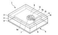
無線タグ1は、矩形板状の基板(誘電体層)2を備えている。基板2は、ガラスエポキシやセラミックスなどの誘電体からなるものである。
この基板2を挟むようにしてアンテナ5が設けられている。アンテナ5は、片面指向性を有するマイクロストリップアンテナである。このアンテナ5は、矩形板状の接地導体4と放射電極9とを備えている。この方式によるアンテナを用いた無線タグは、金属面への取付けに対応するものとなる。
The
An
接地導体4は、基板2の一方の主面(底面)の全面を覆うように設けられている。
放射電極9は、導電体であり、基板2の他方の主面(上面)に設けられている。放射電極9は、接地導体4よりも小さく形成されている。また、放射電極9の一対の長辺部9aは、電波の送受信に寄与する部分であり、その長さ寸法は、通信用電波の波長λの1/4になっている。放射電極9には、切り込み13が形成されている。この切り込み13によって、放射電極9は、接続部15と本体部16とに分けられている。なお、接続部15と本体部16とは直接的には導通していない。
The
The
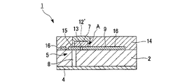
また、放射電極9には、その中心からオフセットした位置にICチップ(集積回路)7が設置されている。ICチップ7は、アンテナ5から電力を供給されて駆動されるものであり、各種情報を記憶する記憶部を有している。この記憶部に記憶された各種情報が、リーダライタなどの外部機器によって読み書きされるようになっている。なお、このICチップ7が設置された領域が、図2に示す設置領域Aとなり、この設置領域Aを囲む領域が周辺領域Bとなる。
Further, the
このICチップ7を介して、接地導体4と放射電極9とが導通している。すなわち、基板2には、その厚さ方向に貫通するスルーホール8が形成され、スルーホール8内にはその長さ方向の全長にわたって導体層(不図示)が設けられている。そして、接続部15と接地導体4とは、導体層に接続されている。さらに、接続部15と本体部16とにわたってICチップ7が設けられている。これにより、本体部16はICチップ7を介して接続部15に電気的に接続され、接続部15は、スルーホール8内の導体層を介して接地導体4に電気的に接続されている。
なお、ICチップ7の厚さ寸法は、100〜150μmに設定されており、この厚さ寸法の分、ICチップ7は放射電極9の上面から、無線タグ1の厚さ方向の上方に突出している。
The
The thickness dimension of the
さらに、基板2の他方の主面及び放射電極9の上面には、絶縁性を有する保護層3が設けられている。保護層3は、基板2の他方の主面及び放射電極9の上面を保護するものである。また、保護層3は、ソルダーレジストからなっている。ソルダーレジストは、絶縁性を有する感光性樹脂であれば何でもよく、通常、エポキシ樹脂系の感光性樹脂組成物に光重合開始剤、希釈剤等を調合したレジストインキが用いられるが、その他の樹脂を使用することもできる。
保護層3は、周辺領域Bに設けられており、設置領域Aには設けられていない。すなわち、保護層3は、ICチップ7及びその周囲を除いて設けられている。
なお、保護層3の厚さ寸法は、20μmに設定されており、ICチップ7は、保護層3の上面からも上方に突出している。
Furthermore, an insulating
The
The thickness dimension of the
さらに、保護層3には、設置領域Aを塞いでICチップ7を覆う被覆部12が設けられている。被覆部12は、樹脂ポッティングにより設けられており、保護層3からドーム状になだらかに突出している。
Further, the
次いで、無線タグ1の製造方法について説明する。
まず、スルーホール形成工程において、基板2の両主面に銅箔が設けられた銅貼積層板に、ドリルなどでスルーホール8を形成する。次いで、導体層形成工程において、無電解メッキにより、スルーホール8内に導体層を形成する。そして、パターニング形成工程により、放射電極9と切り込み13とのパターンを、基板2の他方の主面にマスク露光技術によりパターニングし、不要な銅箔をエッチングにより取り除く。それから、集積回路設置工程において、ICチップ7を設置領域Aに設置する。これによって、接続部15と本体部16とがICチップ7を介して電気的に接続される。
Next, a method for manufacturing the
First, in the through-hole forming step, the through-
さらに、保護層形成工程において、基板2の他方の主面と放射電極9の上面に、設置領域Aを除いて保護層3を設ける。そして、被覆部形成工程において、樹脂ポッティングにより、設置領域Aを塞いでICチップ7を被覆部12で覆う。
これによって、本実施形態における無線タグ1が得られる。
なお、集積回路設置工程の後、保護層形成工程へと移行するものとしたが、これに限ることはなく、保護層形成工程において保護層3を設けた後、集積回路設置工程においてICチップ7を設置してもよい。
Further, in the protective layer forming step, the
Thereby, the
It should be noted that, after the integrated circuit installation step, the process proceeds to the protective layer forming step. However, the present invention is not limited to this, and after the
次に、このように構成された本実施形態における無線タグ1の作用について説明する。
例えば飲料用缶などの物品に、無線タグ1を取り付ける。すなわち、物品の表面と接地導体4の底面とを両面テープなどにより貼り付ける。この状態で、無線タグ1にリーダライタを近接させて、リーダライタから、2.45GHzの電波を放射する。するとアンテナ5は、その電波を受信して、ICチップ7に電力を供給する。これにより、ICチップ7が駆動されて、種々の処理が行われる。すなわち、例えば記憶部に記憶された各種情報が読み出され、その各種情報が搬送波に載せられてアンテナ5を介して放射される。この電波をリーダライタが受信することにより、ICチップ7の各種情報が読み出され、物品の管理などに利用される。
Next, the operation of the
For example, the
ここで、ICチップ7は、放射電極9の上面及び保護層3の上面から突出しているが、被覆部12が設けられていることから、ICチップ7は、被覆部12に覆われて被覆部12の内部に配される。そのため、保護層3に、他の物が擦られるように接触しても、他の物はICチップ7に当接することなく被覆部12の上面を摺動していく。
Here, the
以上より、本実施形態における無線タグ1によれば、ICチップ7が被覆部12に覆われていることから、ICチップ7が、他の物に引っ掛かることを防止することができる。そのため、簡易な構成により、ICチップ7の破損などを効果的に防止することができる。
また、従来のように、無線タグ全体を覆うパッケージなどが不要であることから、迅速かつ容易に製造することができ、コストの上昇を抑制することができる。
また、保護層3が設けられていることから、放射電極9を保護することができるだけでなく、被覆部12を安定かつ確実に設けることができる。
As described above, according to the
Further, unlike the conventional case, a package that covers the entire wireless tag is not required, so that it can be manufactured quickly and easily, and an increase in cost can be suppressed.
Moreover, since the
さらに、被覆部12が樹脂ポッティングにより形成されていることから、既存の設備を利用して容易かつ確実にICチップ7を覆うことができる。すなわち、樹脂ポッティングは、基板を封止するものとして、基板の製造工程において一般的に利用されるものであるから、その樹脂ポッティングを利用して被覆部12を設けることにより、設備や材料などの利用効率を向上させることができる。
また、保護層3がソルダーレジストによりなっていることから、上記と同様に、既存の設備を利用して容易かつ確実に層を形成することができる。
Furthermore, since the covering
Moreover, since the
また、被覆部12がドーム状になだらかに形成されていることから、引っ掛かりを確実に防止することができる。さらに、被覆部12を目視したり、指などで触れることにより、無線タグ1の配置された方向(上下方向)を容易に認識することができる。この場合、被覆部12の色を他の部分(特に保護層3)と異なる色を付すことにより、目視確認をさらに容易にすることができる。
Moreover, since the coating |
なお、本実施形態においては、保護層3がソルダーレジストからなるものとしたが、これに限ることはなく、エポキシ樹脂からなるものとしてもよい。エポキシ樹脂も、基板の製造において一般的に利用される材料であることから、既存の設備や材料などの利用効率を向上させることができる。
In the present embodiment, the
(実施形態2)
次に、本発明の第2の実施形態について説明する。
図3は、本発明の第2の実施形態を示したものである。
図3において、図1及び図2に記載の構成要素と同一部分については同一符号を付し、その説明を省略する。
この実施形態と上記第1の実施形態とは基本的構成は同一であり、ここでは異なる点についてのみ説明する。
(Embodiment 2)
Next, a second embodiment of the present invention will be described.
FIG. 3 shows a second embodiment of the present invention.
In FIG. 3, the same components as those shown in FIGS. 1 and 2 are denoted by the same reference numerals, and the description thereof is omitted.
This embodiment and the first embodiment have the same basic configuration, and only the differences will be described here.
本実施形態における保護層14は、エポキシ樹脂によりなるものである。そして、保護層14の厚さ寸法は、ICチップ7の厚さ寸法よりも大きく設定されている。すなわち、ICチップ7は、保護層14の上面よりも下方に没した状態になっている。この状態において、被覆部12´は設置領域Aを塞いでICチップ7を覆っている。被覆部12´の上面は、平坦面とされており、保護層14の上面と面一にされている。
The
以上より、本実施形態における無線タグ1によれば、被覆部12´の上面と保護層14の上面とが面一にされていることから、被覆部12´の引っ掛かりを確実に防止することができる。
なお、保護層14がエポキシ樹脂によりなっていることから、既存の設備や材料を利用することができるだけでなく、ICチップ7の高さ寸法よりも大きな厚さ寸法を有する層を容易に形成することができる。
As described above, according to the
Since the
なお、本実施形態における無線タグ1を製造する場合、被覆部形成工程において、樹脂ポッティングにより、被覆部12を設けたのち、研磨工程において、被覆部12及び保護層14の表面を研磨してもよい。
When manufacturing the
また、上記第1及び第2の実施形態においては、通信用電波の周波数として、2.45GHzとしているが、これに限ることはなく、他の周波数であってもよい。例えば、950MHzや5.8GHzとすることもできる。
また、保護層3は、少なくとも放射電極9を覆っていればよいが、さらに基板2も覆っていることが好ましい。
さらに、接地導体4及び放射電極9が矩形状としたが、これに限ることはなく、それら形状は適宜変更可能である。例えば、円形、多角形としてもよい。
なお、本発明の技術範囲は上記の実施形態に限定されるものではなく、本発明の趣旨を逸脱しない範囲において、種々の変更を加えることが可能である。
Moreover, in the said 1st and 2nd embodiment, although it is set as 2.45 GHz as a frequency of the electromagnetic wave for communication, it is not restricted to this, Other frequencies may be sufficient. For example, it can be set to 950 MHz or 5.8 GHz.
Further, the
Furthermore, although the
The technical scope of the present invention is not limited to the above embodiment, and various modifications can be made without departing from the spirit of the present invention.
1 無線タグ
3,14 保護層
4 接地導体
7 ICチップ(集積回路)
9 放射電極
12 被覆部
A 設置領域
B 周辺領域
1
9
Claims (3)
前記集積回路が設置される設置領域及び前記設置領域を囲む周辺領域を有する放射電極と、
前記放射電極を支持する誘電体層と、
前記誘電体層を介して前記放射電極と対向する接地導体と、
前記周辺領域に設けられて前記放射電極を覆う保護層と、
前記設置領域に設けられて前記集積回路を覆う被覆部と
を備え、
前記被覆部は樹脂ポッティングで形成されていて、その上面は保護層の上面と面一にされていることを特徴とする無線タグ。 An integrated circuit;
A radiation electrode having an installation area in which the integrated circuit is installed and a peripheral area surrounding the installation area;
A dielectric layer supporting the radiation electrode;
A grounding conductor facing the radiation electrode via the dielectric layer;
A protective layer provided in the peripheral region and covering the radiation electrode;
A covering portion provided in the installation area and covering the integrated circuit ,
The wireless tag according to claim 1, wherein the covering portion is formed by resin potting, and the upper surface thereof is flush with the upper surface of the protective layer .
Priority Applications (1)
| Application Number | Priority Date | Filing Date | Title |
|---|---|---|---|
| JP2006192752A JP4475258B2 (en) | 2006-07-13 | 2006-07-13 | Wireless tag |
Applications Claiming Priority (1)
| Application Number | Priority Date | Filing Date | Title |
|---|---|---|---|
| JP2006192752A JP4475258B2 (en) | 2006-07-13 | 2006-07-13 | Wireless tag |
Publications (2)
| Publication Number | Publication Date |
|---|---|
| JP2008021147A JP2008021147A (en) | 2008-01-31 |
| JP4475258B2 true JP4475258B2 (en) | 2010-06-09 |
Family
ID=39077027
Family Applications (1)
| Application Number | Title | Priority Date | Filing Date |
|---|---|---|---|
| JP2006192752A Active JP4475258B2 (en) | 2006-07-13 | 2006-07-13 | Wireless tag |
Country Status (1)
| Country | Link |
|---|---|
| JP (1) | JP4475258B2 (en) |
-
2006
- 2006-07-13 JP JP2006192752A patent/JP4475258B2/en active Active
Also Published As
| Publication number | Publication date |
|---|---|
| JP2008021147A (en) | 2008-01-31 |
Similar Documents
| Publication | Publication Date | Title |
|---|---|---|
| EP1921570B1 (en) | Radio frequency integrated circuit tag and method of using the RFIC/RFID tag | |
| EP1622069B1 (en) | Radio frequency IC tag and bolt with an IC tag | |
| KR101108940B1 (en) | Rfid tag | |
| US7586446B2 (en) | IC tag-bearing wiring board and method of fabricating the same | |
| US20060151619A1 (en) | Information processing apparatus with contactless reader/writer, and coil antenna for magnetic coupling | |
| US9317800B2 (en) | Non-contact IC label and nameplate | |
| JP2010074809A (en) | Antenna structure for rfid transponder | |
| JP2006174151A (en) | Ic tag and ic tag attaching structure | |
| JP2008042379A (en) | Wireless tag and flexible circuit board therefor | |
| JP2006319964A (en) | Patch antenna for rfid tag | |
| JP2000077928A (en) | Loop antenna and data carrier | |
| JP5637004B2 (en) | Semiconductor integrated circuit module, wireless communication module, and wireless communication device | |
| JP4475258B2 (en) | Wireless tag | |
| KR20090043077A (en) | Antenna for radio frequency identification and method of manufacturing the same | |
| JP2006309324A (en) | Radio tag | |
| JP4781871B2 (en) | Non-contact IC label | |
| JP5098588B2 (en) | Non-contact type IC tag and method of manufacturing non-contact type IC tag | |
| JP5061712B2 (en) | Non-contact IC tag manufacturing method | |
| KR101025771B1 (en) | Radio frequency identification tag and method for manufacturing it | |
| JP5195241B2 (en) | Heat-resistant IC tag strap | |
| JP2008067037A (en) | Antenna device, antenna assembly device, and reader/writer device | |
| KR101427339B1 (en) | RFID card and preparing method for the same | |
| JP7314626B2 (en) | RF tag | |
| JP2009025916A (en) | Wireless ic device | |
| JP4715823B2 (en) | RFID tag |
Legal Events
| Date | Code | Title | Description |
|---|---|---|---|
| A977 | Report on retrieval |
Free format text: JAPANESE INTERMEDIATE CODE: A971007 Effective date: 20090430 |
|
| A131 | Notification of reasons for refusal |
Free format text: JAPANESE INTERMEDIATE CODE: A131 Effective date: 20090623 |
|
| A521 | Request for written amendment filed |
Free format text: JAPANESE INTERMEDIATE CODE: A523 Effective date: 20090821 |
|
| TRDD | Decision of grant or rejection written | ||
| A01 | Written decision to grant a patent or to grant a registration (utility model) |
Free format text: JAPANESE INTERMEDIATE CODE: A01 Effective date: 20100216 |
|
| A01 | Written decision to grant a patent or to grant a registration (utility model) |
Free format text: JAPANESE INTERMEDIATE CODE: A01 |
|
| A61 | First payment of annual fees (during grant procedure) |
Free format text: JAPANESE INTERMEDIATE CODE: A61 Effective date: 20100301 |
|
| R150 | Certificate of patent or registration of utility model |
Ref document number: 4475258 Country of ref document: JP Free format text: JAPANESE INTERMEDIATE CODE: R150 Free format text: JAPANESE INTERMEDIATE CODE: R150 |
|
| FPAY | Renewal fee payment (event date is renewal date of database) |
Free format text: PAYMENT UNTIL: 20130319 Year of fee payment: 3 |
|
| FPAY | Renewal fee payment (event date is renewal date of database) |
Free format text: PAYMENT UNTIL: 20140319 Year of fee payment: 4 |
|
| R250 | Receipt of annual fees |
Free format text: JAPANESE INTERMEDIATE CODE: R250 |
|
| R250 | Receipt of annual fees |
Free format text: JAPANESE INTERMEDIATE CODE: R250 |
|
| R250 | Receipt of annual fees |
Free format text: JAPANESE INTERMEDIATE CODE: R250 |