JP4464397B2 - Bistable microswitch with low power consumption - Google Patents
Bistable microswitch with low power consumption Download PDFInfo
- Publication number
- JP4464397B2 JP4464397B2 JP2006516357A JP2006516357A JP4464397B2 JP 4464397 B2 JP4464397 B2 JP 4464397B2 JP 2006516357 A JP2006516357 A JP 2006516357A JP 2006516357 A JP2006516357 A JP 2006516357A JP 4464397 B2 JP4464397 B2 JP 4464397B2
- Authority
- JP
- Japan
- Prior art keywords
- microswitch
- electrical contact
- conductive tracks
- microswitch according
- forming means
- Prior art date
- Legal status (The legal status is an assumption and is not a legal conclusion. Google has not performed a legal analysis and makes no representation as to the accuracy of the status listed.)
- Expired - Lifetime
Links
- 239000000758 substrate Substances 0.000 claims abstract description 28
- 238000010438 heat treatment Methods 0.000 claims description 26
- 230000009977 dual effect Effects 0.000 claims description 24
- 230000001939 inductive effect Effects 0.000 claims description 19
- 230000000694 effects Effects 0.000 claims description 12
- 239000000463 material Substances 0.000 claims description 9
- 230000004913 activation Effects 0.000 claims description 7
- 239000004020 conductor Substances 0.000 claims description 5
- 239000004065 semiconductor Substances 0.000 claims description 5
- 239000003989 dielectric material Substances 0.000 claims description 3
- 238000005530 etching Methods 0.000 description 14
- 229910004298 SiO 2 Inorganic materials 0.000 description 13
- 238000001459 lithography Methods 0.000 description 10
- 230000008901 benefit Effects 0.000 description 8
- 239000010931 gold Substances 0.000 description 7
- ATJFFYVFTNAWJD-UHFFFAOYSA-N Tin Chemical compound [Sn] ATJFFYVFTNAWJD-UHFFFAOYSA-N 0.000 description 5
- 238000000151 deposition Methods 0.000 description 5
- PCHJSUWPFVWCPO-UHFFFAOYSA-N gold Chemical compound [Au] PCHJSUWPFVWCPO-UHFFFAOYSA-N 0.000 description 5
- 229910052737 gold Inorganic materials 0.000 description 5
- 229910052751 metal Inorganic materials 0.000 description 5
- 239000002184 metal Substances 0.000 description 5
- XUIMIQQOPSSXEZ-UHFFFAOYSA-N Silicon Chemical compound [Si] XUIMIQQOPSSXEZ-UHFFFAOYSA-N 0.000 description 4
- 230000015572 biosynthetic process Effects 0.000 description 4
- 238000004519 manufacturing process Methods 0.000 description 4
- 229910052710 silicon Inorganic materials 0.000 description 4
- 239000010703 silicon Substances 0.000 description 4
- PXHVJJICTQNCMI-UHFFFAOYSA-N Nickel Chemical compound [Ni] PXHVJJICTQNCMI-UHFFFAOYSA-N 0.000 description 3
- PNEYBMLMFCGWSK-UHFFFAOYSA-N aluminium oxide Inorganic materials [O-2].[O-2].[O-2].[Al+3].[Al+3] PNEYBMLMFCGWSK-UHFFFAOYSA-N 0.000 description 3
- 238000003780 insertion Methods 0.000 description 3
- 230000037431 insertion Effects 0.000 description 3
- 238000009413 insulation Methods 0.000 description 3
- 230000010354 integration Effects 0.000 description 3
- 238000001465 metallisation Methods 0.000 description 3
- 238000004377 microelectronic Methods 0.000 description 3
- XEEYBQQBJWHFJM-UHFFFAOYSA-N Iron Chemical compound [Fe] XEEYBQQBJWHFJM-UHFFFAOYSA-N 0.000 description 2
- 239000004642 Polyimide Substances 0.000 description 2
- 229910052782 aluminium Inorganic materials 0.000 description 2
- XAGFODPZIPBFFR-UHFFFAOYSA-N aluminium Chemical compound [Al] XAGFODPZIPBFFR-UHFFFAOYSA-N 0.000 description 2
- 238000005516 engineering process Methods 0.000 description 2
- 238000000034 method Methods 0.000 description 2
- 238000000206 photolithography Methods 0.000 description 2
- 238000000623 plasma-assisted chemical vapour deposition Methods 0.000 description 2
- 238000005498 polishing Methods 0.000 description 2
- 229920001721 polyimide Polymers 0.000 description 2
- 238000003825 pressing Methods 0.000 description 2
- 239000000126 substance Substances 0.000 description 2
- RYGMFSIKBFXOCR-UHFFFAOYSA-N Copper Chemical compound [Cu] RYGMFSIKBFXOCR-UHFFFAOYSA-N 0.000 description 1
- 229910001218 Gallium arsenide Inorganic materials 0.000 description 1
- 230000008859 change Effects 0.000 description 1
- 239000010949 copper Substances 0.000 description 1
- 229910052802 copper Inorganic materials 0.000 description 1
- 230000008878 coupling Effects 0.000 description 1
- 238000010168 coupling process Methods 0.000 description 1
- 238000005859 coupling reaction Methods 0.000 description 1
- 230000008021 deposition Effects 0.000 description 1
- 238000004070 electrodeposition Methods 0.000 description 1
- 238000005868 electrolysis reaction Methods 0.000 description 1
- 230000005284 excitation Effects 0.000 description 1
- 230000005669 field effect Effects 0.000 description 1
- 230000017525 heat dissipation Effects 0.000 description 1
- 229910052742 iron Inorganic materials 0.000 description 1
- 230000001788 irregular Effects 0.000 description 1
- 239000000696 magnetic material Substances 0.000 description 1
- 239000011159 matrix material Substances 0.000 description 1
- 239000007769 metal material Substances 0.000 description 1
- 229910052759 nickel Inorganic materials 0.000 description 1
- 230000003647 oxidation Effects 0.000 description 1
- 238000007254 oxidation reaction Methods 0.000 description 1
- 238000007747 plating Methods 0.000 description 1
- 229910021420 polycrystalline silicon Inorganic materials 0.000 description 1
- 230000004044 response Effects 0.000 description 1
- 230000003068 static effect Effects 0.000 description 1
- 230000000930 thermomechanical effect Effects 0.000 description 1
- 238000001771 vacuum deposition Methods 0.000 description 1
Images


Classifications
-
- H—ELECTRICITY
- H01—ELECTRIC ELEMENTS
- H01H—ELECTRIC SWITCHES; RELAYS; SELECTORS; EMERGENCY PROTECTIVE DEVICES
- H01H1/00—Contacts
- H01H1/0036—Switches making use of microelectromechanical systems [MEMS]
-
- H—ELECTRICITY
- H01—ELECTRIC ELEMENTS
- H01H—ELECTRIC SWITCHES; RELAYS; SELECTORS; EMERGENCY PROTECTIVE DEVICES
- H01H1/00—Contacts
- H01H1/0036—Switches making use of microelectromechanical systems [MEMS]
- H01H2001/0042—Bistable switches, i.e. having two stable positions requiring only actuating energy for switching between them, e.g. with snap membrane or by permanent magnet
-
- H—ELECTRICITY
- H01—ELECTRIC ELEMENTS
- H01H—ELECTRIC SWITCHES; RELAYS; SELECTORS; EMERGENCY PROTECTIVE DEVICES
- H01H61/00—Electrothermal relays
- H01H2061/006—Micromechanical thermal relay
-
- H—ELECTRICITY
- H01—ELECTRIC ELEMENTS
- H01H—ELECTRIC SWITCHES; RELAYS; SELECTORS; EMERGENCY PROTECTIVE DEVICES
- H01H59/00—Electrostatic relays; Electro-adhesion relays
- H01H59/0009—Electrostatic relays; Electro-adhesion relays making use of micromechanics
Landscapes
- Physics & Mathematics (AREA)
- Electromagnetism (AREA)
- Micromachines (AREA)
- Thermally Actuated Switches (AREA)
- Liquid Crystal (AREA)
- Polymers With Sulfur, Phosphorus Or Metals In The Main Chain (AREA)
- Polyesters Or Polycarbonates (AREA)
Abstract
Description
本発明は、水平方向に移動するような、電力消費量の小さな双安定型マイクロスイッチに関するものである。 The present invention relates to a bistable microswitch that moves in the horizontal direction and has low power consumption.
そのようなマイクロスイッチは、特に、携帯電話の分野においておよび宇宙工学の分野において、有効なものである。 Such microswitches are particularly effective in the field of mobile phones and in the field of space engineering.
これら分野における使用を意図したRF素子は、以下のような仕様を満たす必要がある。
−5ボルト未満という供給電圧。
−30dBよりも大きな絶縁性能。
−0.3dB未満という挿入損失。
−109 よりも多くのサイクルに対応する信頼性。
−0.05mm2 未満という表面積。
−できるだけ小さな電力消費。
An RF element intended for use in these fields needs to satisfy the following specifications.
Supply voltage of less than -5 volts.
Insulation performance greater than -30 dB.
Insertion loss of less than -0.3 dB.
Reliability for more than -10 9 cycles.
Surface area that -0.05mm less than 2.
-As little power consumption as possible.
特に宇宙工学の分野の場合には、例えば設備の破損といったような状況において、ある状態から他の状態へのスイッチングを行うために、いくつかのスイッチを一度だけ使用する。この種の用途においては、現在、ある状態から他の状態へとスイッチングされた後に電力供給を必要としないような双安定型スイッチに、非常に大きな興味が存在する。 Particularly in the field of space engineering, some switches are used only once to switch from one state to another in situations such as equipment breakage. In this type of application, there is currently a great interest in bistable switches that do not require power supply after being switched from one state to another.
また、重要な機能の場合に使用される冗長回路のスイッチマトリクスをかなり単純化するようなデュアルスイッチに、大きな興味が存在する。この種の用途は、特に、宇宙工学の分野(衛星アンテナ)に見受けられる。このようなデュアルスイッチにより、破損の際には、ある電子回路から他の電子回路への入力信号をスイッチングすることができる。したがって、このようなスイッチは、第1組をなす2つの電気トラックを、あるいは、第2組をなす2つの電気トラックを、ある状態から他の状態へとスイッチングすることができる。 There is also great interest in dual switches that considerably simplify the switch matrix of redundant circuits used for critical functions. This type of application is found especially in the field of space engineering (satellite antenna). With such a dual switch, an input signal from one electronic circuit to another electronic circuit can be switched in the event of damage. Thus, such a switch can switch two electrical tracks in a first set or two electrical tracks in a second set from one state to another.
デュアルスイッチは、より少ない構成部材でもって(例えば、10個の冗長機能においては、20個の単一スイッチではなく、10個のデュアルスイッチが、必要とされる)回路を形成し得るという利点を有している。このことは、とりわけ、信頼性試験の回数を低減し得ること、また、組立工数を低減し得ること、また、空きスペースを増大させ得ること、また、全体的なコストを低減化し得ること、を意味する。 The dual switch has the advantage that it can form a circuit with fewer components (e.g. 10 dual switches are required instead of 20 single switches in 10 redundant functions). Have. This means that, among other things, the number of reliability tests can be reduced, the number of assembly steps can be reduced, the free space can be increased, and the overall cost can be reduced. means.
通信の分野においては、従来的なマイクロスイッチ(つまり、マイクロエレクトロニクスにおいて使用されているマイクロスイッチ)は、非常に広範に使用されている。それらマイクロスイッチは、信号分岐ネットワークや、インピーダンスマッチングネットワークや、アンプのゲイン調整、等において有効である。スイッチングすべき信号の周波数帯域は、数MHz〜数十GHzとすることができる。 In the field of communications, conventional microswitches (ie, microswitches used in microelectronics) are very widely used. These microswitches are effective in signal branching networks, impedance matching networks, amplifier gain adjustment, and the like. The frequency band of the signal to be switched can be several MHz to several tens GHz.
従来技術においては、マイクロエレクトロニクススイッチは、RF回路において使用されてきた。このようなスイッチは、回路の集積化を可能とするとともに、製造コストを低減化する。しかしながら、性能という観点においては、これら素子は、制限されている。すなわち、シリコンFETスイッチは、低周波数においては大電力信号をスイッチングし得るものの、高周波数においてはスイッチングを行うことができない。GaAsダイオードやPINダイオードからなるMESFET(Metal Semiconductor Field Effect
Transistor)スイッチは、高周波数においてはうまく動作するものの、低電力の信号にしか適用することができない。結局、一般に、1GHzよりも大きな周波数においては、すべてのマイクロエレクトロニクススイッチは、オン時には、大きな挿入損失(従来技術においては、およそ1〜2dB)を有しているとともに、開放状態においては、かなり小さな絶縁性能(−20〜−25dB)を示す。したがって、これら従来的なスイッチを、MEMS(Micro-Electro-Mechanical-System )マイクロスイッチによって代替することが、このタイプの応用においては期待されるところである。
In the prior art, microelectronic switches have been used in RF circuits. Such a switch allows circuit integration and reduces manufacturing costs. However, these elements are limited in terms of performance. That is, the silicon FET switch can switch a large power signal at a low frequency, but cannot switch at a high frequency. MESFET (Metal Semiconductor Field Effect) consisting of GaAs diodes and PIN diodes
Transistor) switches work well at high frequencies, but can only be applied to low-power signals. Eventually, in general, at frequencies greater than 1 GHz, all microelectronic switches have a large insertion loss (on the order of 1-2 dB in the prior art) when on and are quite small in the open state. Insulation performance (-20 to -25 dB) is shown. Therefore, replacing these conventional switches with MEMS (Micro-Electro-Mechanical-System) microswitches is expected in this type of application.
構成および動作原理の点から、MEMSスイッチは、次のような特性を有している。
−小さな挿入損失(典型的には、0.3dB未満)。
−MHz領域において、ミリメートル範囲(典型的には、−30dBよりも大きい)という大きな絶縁性能。
−レスポンスが非線形的ではないこと(IP3)。
From the viewpoint of configuration and operating principle, the MEMS switch has the following characteristics.
-Small insertion loss (typically less than 0.3 dB).
-Great insulation performance in the millimeter range, typically in the millimeter range (typically greater than -30 dB).
-The response is not non-linear (IP3).
MEMSマイクロスイッチに関しては、2つのタイプのコンタクトが識別される。すなわち、オーミックコンタクトと容量性コンタクトとが、識別される。オーミックコンタクトスイッチにおいては、2つのRFトラックが、短絡(金属と金属との間のコンタクト)によってコンタクトする。このタイプのコンタクトは、連続的な信号においても、また、高周波信号(10GHz以上)においても、適切である。容量性コンタクトスイッチにおいては、閉状態と開状態との間のキャパシタンス変化が得られるように、エアギャップが、電気機械的に調節される。このタイプのコンタクトは、高周波数(10GHz以上)においては特に好適であるものの、低周波数においては不適切である。 With respect to MEMS microswitches, two types of contacts are identified. That is, an ohmic contact and a capacitive contact are distinguished. In an ohmic contact switch, two RF tracks are contacted by a short circuit (a contact between metal). This type of contact is suitable for both continuous signals and high frequency signals (10 GHz and above). In capacitive contact switches, the air gap is adjusted electromechanically to obtain a capacitance change between the closed and open states. This type of contact is particularly suitable at high frequencies (10 GHz and above) but unsuitable at low frequencies.
MEMSスイッチに関するいくつかの主要な駆動原理が識別される。 Several major driving principles for MEMS switches are identified.
代表的なものとして記述し得るような熱駆動型のマイクロスイッチは、双安定性ではない。このようなマイクロスイッチは、駆動電圧が小さいという利点を有している。このようなマイクロスイッチは、いくつかの欠点を有している。すなわち、消費電力が大きく(特に、携帯電話という用途の場合)、スイッチング速度が遅く(熱的な慣性のために)、閉塞位置におけるコンタクトを維持するために供給電圧を必要とする。 Thermally driven microswitches that can be described as representative are not bistable. Such a microswitch has the advantage that the drive voltage is small. Such microswitches have several drawbacks. That is, the power consumption is high (especially for mobile phone applications), the switching speed is slow (due to thermal inertia), and a supply voltage is required to maintain contact in the closed position.
代表的なものとして記述し得るような静電駆動型のマイクロスイッチは、双安定性ではない。このようなマイクロスイッチは、スイッチング速度が速いという利点、および、一般的に単純な技術であるという利点、を有している。このようなマイクロスイッチは、信頼性という点において問題点を有している。特に、低駆動電圧型の静電スイッチ(構造的結合)の場合には、信頼性という点において問題点を有している。また、このようなマイクロスイッチは、閉状態でのコンタクトを維持するために供給電圧を必要とする。 Electrostatically driven microswitches that can be described as representative are not bistable. Such microswitches have the advantage of fast switching speeds and generally simple technology. Such a microswitch has a problem in terms of reliability. In particular, a low driving voltage type electrostatic switch (structural coupling) has a problem in terms of reliability. Such microswitches also require a supply voltage to maintain contact in the closed state.
代表的なものとして記述し得るような電磁駆動型のマイクロスイッチは、双安定性ではない。このようなマイクロスイッチは、一般に、電磁石の原理で動作し、鉄をベースとした磁気回路と磁界コイルとを不可欠的に使用する。このようなマイクロスイッチは、いくつかの欠点を有している。このようなマイクロスイッチに関する技術は、複雑である(コイル、場合によっては永久磁石といったような磁性材料、等)。このようなマイクロスイッチにおいては、電力消費量が大きい。さらに、このようなマイクロスイッチは、閉状態でのコンタクトを維持するために供給電圧を必要とする。 Electromagnetically driven microswitches that can be described as representative are not bistable. Such microswitches generally operate on the principle of an electromagnet and essentially use an iron-based magnetic circuit and a magnetic field coil. Such microswitches have several drawbacks. The technology relating to such a microswitch is complicated (coils, and in some cases, magnetic materials such as permanent magnets, etc.). In such a microswitch, power consumption is large. In addition, such microswitches require a supply voltage to maintain contact in the closed state.
コンタクトを移動させるための2つの構成を識別することができる。すなわち、鉛直方向移動と、水平方向移動と、が存在する。 Two configurations for moving the contacts can be identified. That is, there are vertical movement and horizontal movement.
鉛直方向移動の場合には、移動は、RFトラックがなす平面の外部において起こる。コンタクトは、トラックの上部または底部において、行われる。この構成の利点は、コンタクトパッドの金属化を容易に行い得ること(平面的成膜)である。したがって、コンタクトの抵抗値が小さい。しかしながら、この構成は、デュアルコンタクトスイッチの機能を実現するのには、適していない。頂面上におけるコンタクトは、実際、得ることが困難である。一般に、そのようなコンタクトは、キャップ上のコンタクトを使用することによって得られる。また、この構成は、集積化に対する互換性を有していない。確かに、抵抗性スイッチにおいては、金によって金属化したようなトラックおよびコンタクト(良好な電気的特性を有するとともに、酸化しない)が、従来より使用されている。しかしながら、この金属は、このタイプの構成の初期の時点から使用されているにもかかわらず、集積化には互換的ではない。コンタクトを最適化することはできない。表面は、平面的なものとすることしかできない。コンタクトを形成する梁の硬さは、うまく制御することができない。この硬さは、犠牲層の形状に依存するような梁の最終形状によって調整される。犠牲層の形状自体は、直下に位置するトラックの形状および厚さに依存する。梁の形状は、一般に、不規則的である。このことは、スイッチの硬さを実質的に増大させ、したがって、スイッチの駆動条件を制約する。 In the case of vertical movement, the movement occurs outside the plane formed by the RF track. Contact is made at the top or bottom of the track. The advantage of this configuration is that the contact pad can be easily metallized (planar film formation). Therefore, the contact resistance value is small. However, this configuration is not suitable for realizing the function of the dual contact switch. Contact on the top surface is actually difficult to obtain. In general, such contacts are obtained by using contacts on the cap. Also, this configuration is not compatible with integration. Indeed, in resistive switches, tracks and contacts (which have good electrical properties and do not oxidize), such as those metallized with gold, have been used in the past. However, this metal is not compatible for integration, even though it has been used since the early days of this type of configuration. Contact cannot be optimized. The surface can only be planar. The hardness of the beams forming the contacts cannot be controlled well. This hardness is adjusted by the final shape of the beam depending on the shape of the sacrificial layer. The shape of the sacrificial layer itself depends on the shape and thickness of the track located immediately below. The beam shape is generally irregular. This substantially increases the hardness of the switch and thus limits the drive conditions of the switch.
水平方向移動の場合には、移動は、トラックがなす平面内において起こる。コンタクトは、トラックの側面のところにおいて行われる。この構成は、対称的なアクチュエータを使用した場合には、デュアルコンタクトにおいて好適である。『金』による金属化は、最も最後の技術的ステップにおいて、行うことができる。それ以前に行われるすべてのステップは、集積回路の製造に対して互換的なものとすることができる。コンタクトの形状は、光リソグラフィーステップにおいて、決定される。例えば、円形のコンタクトを形成することができ、これにより、コンタクト抵抗を制限し得るようにして、ある場所でのコンタクトを行うことができる。梁の形状は、光リソグラフィーステップにおいて、決定される。したがって、梁の硬さを、うまく制御することができる。しかしながら、側面上における金属化は、困難である。したがって、コンタクトの抵抗値を、うまく制御することができない。この構成は、双方の駆動面がかなり低減されていることのために、静電駆動には不適切である。 In the case of horizontal movement, the movement occurs in the plane made by the track. Contact is made at the side of the track. This configuration is suitable for dual contact when symmetrical actuators are used. Metallization with “gold” can be done in the last technical step. All previous steps can be made compatible with integrated circuit manufacturing. The shape of the contact is determined in the photolithography step. For example, a circular contact can be formed, thereby making contact at a location so that contact resistance can be limited. The shape of the beam is determined in the photolithography step. Therefore, the hardness of the beam can be controlled well. However, metallization on the side is difficult. Therefore, the resistance value of the contact cannot be controlled well. This configuration is unsuitable for electrostatic drive because both drive surfaces are significantly reduced.
平衡状態の数は、スイッチの移動の他の特性である。典型的な状況においては、アクチュエータは、ただ1つの平衡状態しか有していない。このことは、スイッチの2つの状態のうちの一方の状態(スイッチングされた状態、あるいは、スイッチングされていない状態)において、その状態を保持するために、連続的な電圧供給を必要とすることを、意味している。励起を遮断すると、スイッチは、平衡状態へと戻ってしまう。 The number of equilibrium states is another characteristic of switch movement. In a typical situation, the actuator has only one equilibrium. This means that in one of the two states of the switch (switched or not switched), a continuous voltage supply is required to maintain that state. Mean. When the excitation is cut off, the switch returns to equilibrium.
双安定の場合には、アクチュエータは、互いに異なる2つの平衡状態を有している。この動作モードの利点は、『閉』状態および『開』状態というスイッチの2つの状態が、安定なものであって、一方の状態から他方の状態へのスイッチングを行わない場合には、電力供給が不要であるということである。なお、本出願人の知る限りにおいては、本出願に関連性を有する先行技術文献は存在しない。 In the bistable case, the actuator has two different equilibrium states. The advantage of this mode of operation is that the two states of the switch, the “closed” state and the “open” state, are stable and do not switch from one state to the other. Is unnecessary. To the best of the knowledge of the present applicant, there is no prior art document relevant to the present application.
本発明は、水平方向移動を行うような低電力消費型の双安定型マイクロスイッチを提供する。このマイクロスイッチは、携帯電話という分野においておよび宇宙工学の分野において、特に好適なものである。 The present invention provides a low-power consumption bistable microswitch that performs horizontal movement. This microswitch is particularly suitable in the field of mobile phones and in the field of space engineering.
したがって、本発明の主題は、基板上に形成された双安定型のMEMSマイクロスイッチであって、少なくとも2つの導電トラックの端部どうしを電気的に接続し得るものであり、基板の表面上に懸架された梁を具備し、この梁が、両端部のところにおいて埋設されているとともに、非変形状態においては圧縮応力を受けるものとされ、梁が、電気的コンタクト形成手段を備え、これら電気的コンタクト形成手段が、基板表面に対して平行に梁が変形した際には、2つの導電トラックの端部に対して側方から接触し得るようにして、配置され、マイクロスイッチが、梁を駆動するための駆動手段を具備し、これら駆動手段が、梁を、第1安定状態に対応した第1変形位置へと、または、第2安定状態に対応した第2変形位置へと、配置し、ここで、第1変形位置と第2変形位置とが、非変形状態を挟んで、互いに反対側に位置するものとされ、電気的コンタクト形成手段が、梁がいずれかの変形位置とされた際には、2つの導電トラックの端部を確実に接続する。 Accordingly, the subject of the present invention is a bistable MEMS microswitch formed on a substrate that can electrically connect the ends of at least two conductive tracks on the surface of the substrate. A suspended beam, the beam being embedded at both ends and subjected to compressive stress in the undeformed state, the beam comprising electrical contact forming means, The contact forming means is arranged so that when the beam is deformed parallel to the substrate surface, it can come into contact with the ends of the two conductive tracks from the side, and the microswitch drives the beam. And driving means for disposing the beam to the first deformation position corresponding to the first stable state or the second deformation position corresponding to the second stable state; This Thus, when the first deformation position and the second deformation position are located on opposite sides of the non-deformation state, the electrical contact forming means is set to one of the deformation positions. Reliably connects the ends of the two conductive tracks.
マイクロスイッチは、デュアルマイクロスイッチとすることができる。この場合には、第1変形位置は、第1組をなす2つの導電トラックの各端部を接続する位置に対応し、第2変形位置は、第2組をなす2つの導電トラックの各端部を接続する位置に対応する。 The microswitch can be a dual microswitch. In this case, the first deformation position corresponds to the position where the ends of the two conductive tracks forming the first set are connected, and the second deformation position is the end of each of the two conductive tracks forming the second set. Corresponds to the position where the parts are connected.
マイクロスイッチは、シングルマイクロスイッチとすることができる。この場合には、第1変形位置は、2つの導電トラックの各端部を接続する位置に対応し、第2変形位置は、接続をもたらさない位置に対応する。 The microswitch can be a single microswitch. In this case, the first deformation position corresponds to a position where the ends of the two conductive tracks are connected, and the second deformation position corresponds to a position where no connection is made.
一実施形態においては、梁は、誘電性材料あるいは半導体材料から形成され、電気的コンタクト形成手段は、梁と一体化された導電性パッドから形成される。駆動手段は、バイメタル効果を使用した加熱アクチュエータを備えることができる。各加熱アクチュエータは、熱伝導性材料からなるブロックと、このブロックに対して緊密に接触して配置された電気抵抗部材と、を備えることができる。駆動手段は、静電力を誘起するための手段を備えることができる。駆動手段は、バイメタル効果を使用した加熱アクチュエータと、静電力を誘起するための手段と、を備えることができる。 In one embodiment, the beam is formed from a dielectric or semiconductor material and the electrical contact forming means is formed from a conductive pad integrated with the beam. The driving means can include a heating actuator using a bimetal effect. Each heating actuator can include a block made of a thermally conductive material and an electrical resistance member disposed in intimate contact with the block. The drive means can comprise means for inducing an electrostatic force. The driving means can include a heating actuator using a bimetal effect and a means for inducing an electrostatic force.
他の実施形態においては、梁は、導電性材料から形成される。駆動手段は、静電力を誘起するための手段を備えることができる。 In other embodiments, the beam is formed from a conductive material. The drive means can comprise means for inducing an electrostatic force.
電気的コンタクト形成手段は、接続すべき導電トラックの端部間に嵌め込まれ得るような形状を有することができる。この場合、導電トラックの端部は、接続時に電気的コンタクト形成手段の形状に適合することを可能とし得るよう、フレキシブルさを有することができる。 The electrical contact forming means can have a shape that can be fitted between the ends of the conductive tracks to be connected. In this case, the end of the conductive track can be flexible so that it can be adapted to the shape of the electrical contact forming means when connected.
マイクロスイッチは、さらに、梁の埋設された少なくとも1つの端部のための解放スプリング形成手段を具備することができる。 The microswitch can further comprise a release spring forming means for at least one embedded end of the beam.
電気的コンタクト形成手段は、オーミックコンタクトをもたらし得るようなまたは容量性コンタクトをもたらし得るような、手段とすることができる。 The electrical contact forming means can be a means that can provide an ohmic contact or can provide a capacitive contact.
添付図面を参照しつつ、本発明を何ら限定するものではなく単なる例示としての好ましい実施形態に関する以下の詳細な説明を読むことにより、本発明が、より明瞭に理解され、本発明の他の利点や特徴点が、明らかとなるであろう。 The invention will be more clearly understood and other advantages of the invention will become apparent upon reading the following detailed description of the preferred embodiments, which are given by way of illustration only and not by way of limitation, with reference to the accompanying drawings, in which: And features will be clear.
以下の説明は、例示として、オーミックコンタクトマイクロスイッチに関するものである。しかしながら、当業者であれば、本発明を容量性コンタクトマイクロスイッチに対して容易に適用し得ることは、理解されるであろう。 The following description relates to an ohmic contact microswitch as an example. However, those skilled in the art will appreciate that the present invention can be readily applied to capacitive contact microswitches.
図1は、本発明によるデュアルマイクロスイッチの第1実施形態を示す平面図である。 FIG. 1 is a plan view showing a first embodiment of a dual microswitch according to the present invention.
マイクロスイッチは、基板1上に形成されている。基板1は、図1においては、図示の単純化のために、その一部だけが図示されている。このマイクロスイッチは、デュアルスイッチである。このマイクロスイッチは、導電トラック2,3の端部12,13の間を接続することまたは導電トラック4,5の端部14,15の間を接続することのいずれかを行い得るよう、意図されたものである。
The microswitch is formed on the substrate 1. Only a part of the substrate 1 is shown in FIG. 1 for the sake of simplicity. This microswitch is a dual switch. This microswitch is intended to be able to either connect between the
図1のマイクロスイッチは、誘電性材料あるいは半導体材料から形成された梁6を備えている。梁6は、導電トラックがなす平面内に位置している。この梁6の両端部は、基板1の高所部分に埋め込まれている。図1においては、梁は、初期状態で図示されている。梁は、その後、圧縮応力を受けることとなる。この応力は、マイクロスイッチの可動構造つまり梁とこの梁に関連する部材(アクチュエータ)とを形成するために使用されている材料の本来的応力によって、引き起こすことができる。 The microswitch shown in FIG. 1 includes a beam 6 made of a dielectric material or a semiconductor material. The beam 6 is located in a plane formed by the conductive track. Both ends of the beam 6 are embedded in the high portion of the substrate 1. In FIG. 1, the beam is shown in an initial state. The beam will then be subjected to compressive stress. This stress can be caused by the inherent stress of the material used to form the movable structure of the microswitch, i.e. the beam and the member (actuator) associated with the beam.
図示されている梁は、矩形横断面形状を有するものとされている。梁のうちの、導電トラック2,3を向いた面(すなわち、梁の一方の側面)上においては、梁は、アクチュエータ20,30を支持している。梁のうちの、導電トラック4,5を向いた面(すなわち、梁の他方の側面)上においては、梁は、アクチュエータ40,50を支持している。アクチュエータは、梁の埋設領域の近傍に配置されている。各アクチュエータは、電気抵抗値を有した熱伝導ブロックから構成されている。すなわち、アクチュエータ20は、電気抵抗部材22が接続されているブロック21を備えている。同じことは、他のアクチュエータに対しても、当てはまる。
The illustrated beam has a rectangular cross-sectional shape. On the surface of the beam that faces the conductive tracks 2 and 3 (that is, one side surface of the beam), the beam supports the
梁は、好ましくは、熱膨張係数の小さな誘電性材料あるいは半導体材料から形成される。加熱アクチュエータをなすブロックは、好ましくは、熱膨張係数の大きな金属材料から形成される。これにより、効果的なバイメタル効果を得ることができる。水平方向(図面がなす平面)において梁を移動させる際には、アクチュエータは、梁の埋設部分の近傍のところにおいて梁の両端部のところに配置される。これにより、熱機械的な効果を、常に効果的なものとすることができる。 The beam is preferably formed from a dielectric material or semiconductor material having a low coefficient of thermal expansion. The block forming the heating actuator is preferably made of a metal material having a large coefficient of thermal expansion. Thereby, an effective bimetal effect can be obtained. When the beam is moved in the horizontal direction (the plane formed by the drawing), the actuator is disposed at both ends of the beam in the vicinity of the embedded portion of the beam. Thereby, the thermomechanical effect can be always effective.
梁6は、さらに、中央部分においてかつ一方の側面上において、電気的コンタクトパッド7を支持している。この電気的コンタクトパッド7は、トラック2,3の端部12,13の間の電気的オーミック接続をもたらすことを意図したものである。梁6は、さらに、中央部分においてかつ他方の側面上において、電気的コンタクトパッド8を支持している。この電気的コンタクトパッド8は、トラック4,5の端部14,15の間の電気的オーミック接続をもたらすことを意図したものである。
The beam 6 further supports an electrical contact pad 7 in the central part and on one side. This electrical contact pad 7 is intended to provide an electrical ohmic connection between the
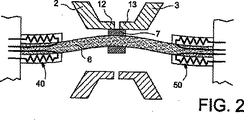
マイクロスイッチが起動されたときには、第1組をなす複数のアクチュエータにより、梁6を、2つの安定状態のうちの一方の安定状態に対応した位置へと、スイッチングすることができる。この状況は、図2に示されている。アクチュエータ40,50は、梁6に対して、バイメタル効果をもたらしている。これにより、梁が変形を受け、梁は、図2に示すように、第1安定状態へと移動している。この安定状態においては、電気的コンタクトパッド7は、導電トラック2,3の端部12,13の間の接続を行っている。アクチュエータ40,50の電気抵抗部材に対する電力供給を停止しても、梁は、この第1安定状態を維持する。
When the microswitch is activated, the beam 6 can be switched to a position corresponding to one of the two stable states by the first set of actuators. This situation is illustrated in FIG. The
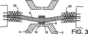
マイクロスイッチをスイッチングするには、すなわち、マイクロスイッチを第2安定状態へと移動させるには、アクチュエータ20,30の電気抵抗部材に対して電力を供給しなければならない。これにより、梁6に対して、上記とは逆向きのバイメタル効果を誘起することができる。これにより、梁が変形し、梁は、図3に示すように、第2安定状態へと移動する。この第2安定状態においては、電気的コンタクトパッド8は、導電トラック4,5の端部14,15の間の接続を行う。アクチュエータ20,30の電気抵抗部材に対する電力供給を停止しても、梁は、この第2安定状態を維持する。
In order to switch the microswitch, that is, to move the microswitch to the second stable state, electric power must be supplied to the electric resistance members of the
アクチュエータの電気抵抗部材は、好ましくは、大きな電気抵抗値を有した導電材料から形成される。導電トラックおよびコンタクトパッドは、好ましくは、金から形成される。その理由は、良好な電気的特性を有するとともに、特に酸化に対する耐性といったように、経時的な信頼性を有しているからである。 The electric resistance member of the actuator is preferably formed from a conductive material having a large electric resistance value. The conductive tracks and contact pads are preferably formed from gold. This is because it has good electrical characteristics and reliability over time such as resistance to oxidation.
梁の埋設領域は、剛直なものとすることができる(単純な埋設)。あるいは、梁の埋設領域は、例えば解放スプリングの付加といったような手法によって、埋設領域の構成を変更することにより、いささかフレキシブルなものとすることができる。梁のフレキシブルさを調節し得ることにより、梁内の応力を、初期的に(本来的応力)制御することができ、梁を、一方の安定状態から(座屈状態を経由して)他方の安定状態へと移行させることができる。このことは、梁の破損というリスクを制限し得るだけでなく、マイクロスイッチの電力消費量を制限し得る(マイクロスイッチのスイッチング温度を低下させ得ることによる)という、利点を有している。梁の応力は、埋設端部の一方のみにおいても、また、埋設端部の双方においても、緩和することができる。 The beam embedding area can be rigid (simple embedding). Alternatively, the embedded region of the beam can be made somewhat flexible by changing the configuration of the embedded region, for example, by adding a release spring. By being able to adjust the flexibility of the beam, the stress in the beam can be controlled initially (intrinsic stress), and the beam can be controlled from one stable state (via the buckled state) to the other. It is possible to shift to a stable state. This not only can limit the risk of beam breakage, but also has the advantage that it can limit the power consumption of the microswitch (by reducing the switching temperature of the microswitch). The stress of the beam can be relieved only at one of the embedded ends or at both of the embedded ends.
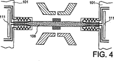
図4は、本発明によるデュアルマイクロスイッチの第2実施形態を示す平面図であって、この実施形態においては、梁の2つの端部は、応力が緩和された埋設領域を備えている。 FIG. 4 is a plan view showing a second embodiment of the dual microswitch according to the present invention. In this embodiment, the two ends of the beam are provided with buried regions where stress is relaxed.
図4の実施形態は、図2の実施形態の場合と同じ複数の構成部材を備えている。しかしながら、梁の端部の埋設領域の構成に関しては、相違している。埋設領域のところにおいては、基板1は、梁の長手方向軸線に対して直交する応力緩和スロット111を備えている。スロット111は、基板のうちの、スロットと梁との間に位置した部分に対して、いくらかのフレキシブルさを付与する。マイクロスイッチは、図4においては、起動前の初期状態でもって図示されている。
The embodiment of FIG. 4 includes the same plurality of components as in the embodiment of FIG. However, the configuration of the buried region at the end of the beam is different. At the buried region, the substrate 1 is provided with
静電気力を、本発明によるマイクロスイッチの駆動原理として使用することができる。あるいは、静電気力を、アクチュエータの加熱用電気抵抗部材に対する電力供給の停止後に、スイッチング後の位置における補助力として使用することができる。これにより、電気的コンタクトパッドの押圧力を増大させることができ、これにより、コンタクト抵抗値を低減することができる。 The electrostatic force can be used as the driving principle of the microswitch according to the present invention. Alternatively, the electrostatic force can be used as an auxiliary force at the position after switching after the power supply to the heating electric resistance member of the actuator is stopped. Thereby, the pressing force of the electrical contact pad can be increased, and thereby the contact resistance value can be reduced.
図5は、本発明によるデュアルマイクロスイッチの第3実施形態を示す平面図である。このマイクロスイッチは、バイメタル効果アクチュエータと、静電的補助力と、を使用する。マイクロスイッチは、図5においては、起動前の初期状態でもって図示されている。 FIG. 5 is a plan view showing a third embodiment of the dual microswitch according to the present invention. This microswitch uses a bimetallic effect actuator and an electrostatic assist force. The microswitch is shown in FIG. 5 in an initial state before activation.
基板201が図示されており、さらに、梁206を第1安定状態へとスイッチングした時に電気的コンタクトパッド207によって接続されることとなるトラック202,203が図示されており、さらに、梁206を第2安定状態へとスイッチングした時に電気的コンタクトパッド208によって接続されることとなるトラック204,205が図示されており、さらに、アクチュエータ220,230,240,250が図示されている。
A
図5のマイクロスイッチは、さらに、静電気力の適用を可能とするための電極を備えている。これら電極は、梁上と基板上とに配置されている。梁206は、第1側面上においては、電極261,262を支持しており、第2側面上においては、電極263,264を支持している。これら電極は、加熱アクチュエータと電気的コンタクトパッドとの間に配置されている。基板201は、梁206によって支持されている各電極に対向させつつ、電極271〜274を支持している。電極271は、電極261に対向した部分を有している。この部分は、図面上では見えない部分である。電極271は、さらに、電気的接続を意図した部分を有している。この部分は、図面上で見える部分である。同じことは、電極262,263,264に対してそれぞれ対向した電極272,273,274に関しても、当てはまる。
The microswitch of FIG. 5 further includes an electrode for enabling application of electrostatic force. These electrodes are arranged on the beam and on the substrate. The
電極271〜274が、変形した梁の形状に対応する形状を有していることに注意されたい。これにより、駆動電圧あるいは維持電圧を低減することができる(可変ギャップ電極)。
Note that the
マイクロスイッチは、加熱アクチュエータ240,250を使用することによって、例えば電気的コンタクトパッド207による導電トラック202,203の接続に対応したような第1安定状態に、配置することができる。加熱アクチュエータ240,250は、第1安定状態を達成する際にのみ起動される。電極261,271間への、および、電極262,272間への、電圧供給により、パッド207とトラック202,203との間のコンタクト抵抗値を確実に低減することができる。
The microswitch can be placed in a first stable state, for example corresponding to the connection of the
マイクロスイッチは、加熱アクチュエータ220,230を使用することによって、第2安定状態へと、配置することができる。加熱アクチュエータ220,230は、第1安定状態から第2安定状態へのスイッチングを達成する際にのみ起動される。電極263,273間への、および、電極264,274間への、電圧供給により、パッド208とトラック204,205との間のコンタクト抵抗値を確実に低減することができる。
The microswitch can be placed into the second stable state by using the
図6は、本発明によるシングルマイクロスイッチを示す平面図である。このマイクロスイッチにおいては、バイメタル効果アクチュエータを使用しており、静電的補助力は使用していない。マイクロスイッチは、図6においては、起動前の初期状態でもって図示されている。 FIG. 6 is a plan view showing a single microswitch according to the present invention. In this microswitch, a bimetal effect actuator is used, and no electrostatic auxiliary force is used. The microswitch is illustrated in FIG. 6 with an initial state before activation.
基板301が図示されており、さらに、梁306を第1安定状態へとスイッチングした時に電気的コンタクトパッド307によって接続されることとなるトラック302,303が図示されている。第2安定状態は、接続を行わない状態に対応している。さらに、アクチュエータ320,330,340,350が図示されている。
A
図7は、本発明によるデュアルマイクロスイッチの第4実施形態を示す平面図である。このマイクロスイッチは、静電効果アクチュエータのみを使用する。マイクロスイッチは、図7においては、起動前の初期状態でもって図示されている。 FIG. 7 is a plan view showing a fourth embodiment of the dual microswitch according to the present invention. This microswitch uses only electrostatic effect actuators. The microswitch is illustrated in FIG. 7 with an initial state before activation.
基板401が図示されており、さらに、梁406を第1安定状態へとスイッチングした時に電気的コンタクトパッド407によって接続されることとなるトラック402,403が図示されており、さらに、梁406を第2安定状態へとスイッチングした時に電気的コンタクトパッド408によって接続されることとなるトラック404,405が図示されている。
A
図7のマイクロスイッチは、静電力の適用を可能とする電極を備えている。これら電極は、梁上と基板上とに配置されている。梁406は、第1側面上においては、電極461,462を支持しており、第2側面上においては、電極463,464を支持している。これら電極は、電気的コンタクトパッド407,408の両サイドに配置されている。基板401は、梁406によって支持されている各電極に対向させつつ、電極471〜474を支持している。電極471は、電極461に対向した部分を有している。この部分は、図面上では見えない部分である。電極471は、さらに、電気的接続を意図した部分を有している。この部分は、図面上で見える部分である。同じことは、電極462,463,464に対してそれぞれ対向した電極472,473,474に関しても、当てはまる。
The microswitch of FIG. 7 includes an electrode that enables application of electrostatic force. These electrodes are arranged on the beam and on the substrate. The
マイクロスイッチは、電極461,471間へとおよび電極462,472間へと電圧を印加することにより、例えば電気的コンタクトパッド407による導電トラック402,403の接続に対応したような第1安定状態に、配置することができる。第1安定状態へと梁をスイッチングした後には、印加電圧を解除または低減することができる。これにより、パッド407とトラック402,403との間のコンタクト抵抗値を低減することができる。
The microswitch is applied to a voltage between the
マイクロスイッチは、電極463,473間へとおよび電極464,474間へと電圧を印加することにより、第2安定状態に配置することができる(ここで、マイクロスイッチを第1安定状態に維持するために静電力を使用していたのであれば、その静電力のための印加電圧は、解除する)。第2安定状態へと梁をスイッチングした後には、上記の場合と同様に、印加電圧を解除または低減することができる。
The microswitch can be placed in the second stable state by applying a voltage between the
図8は、本発明によるデュアルマイクロスイッチの第5実施形態を示す平面図である。この第5実施形態は、上記第4実施形態を最適化した実施形態である。上記第4実施形態と同じ符号を使用することによって、同じ部材を表している。 FIG. 8 is a plan view showing a fifth embodiment of the dual microswitch according to the present invention. The fifth embodiment is an optimized version of the fourth embodiment. By using the same reference numerals as in the fourth embodiment, the same members are represented.
電極471’,472’,473’,474’は、図7のマイクロスイッチにおけるそれぞれ対応する電極471,472,473,474と同じ機能を有している。しかしながら、これら電極471’,472’,473’,474’は、変形後の梁の形状に対応した形状を有している。これにより、駆動電圧あるいは維持電圧を低減することができる(可変ギャップ電極)。
The electrodes 471 ', 472', 473 ', and 474' have the same functions as the corresponding
図9は、本発明によるデュアルマイクロスイッチの第6実施形態を示す平面図である。このマイクロスイッチは、図9においては、起動前の初期状態でもって図示されている。 FIG. 9 is a plan view showing a sixth embodiment of a dual microswitch according to the present invention. This microswitch is shown in FIG. 9 in an initial state before activation.
基板501が図示されており、さらに、梁506を第1安定状態へとスイッチングした時に電気的コンタクトパッド507によって接続されることとなるトラック502,503が図示されており、さらに、梁506を第2安定状態へとスイッチングした時に電気的コンタクトパッド508によって接続されることとなるトラック504,505が図示されている。
A
この実施形態においては、梁506は、金属からなる梁とされており、例えばアルミニウムからなる梁とされている。梁の側面上には、コンタクトパッド507,508が支持されている。例えば導電トラック502,503の接続に対応したような第1安定状態への梁のスイッチングは、電極として作用する梁506と、電極571,572と、の間へとスイッチング電圧を印加することにより、得られる。第1安定状態へと梁をスイッチングした後には、印加電圧を解除または低減することができる。これにより、パッド507とトラック502,503との間のコンタクト抵抗値を低減することができる。
In this embodiment, the
マイクロスイッチは、梁506と電極573,574との間へと電圧を印加することにより、第2安定状態に配置することができる(ここで、マイクロスイッチを第1安定状態に維持するために静電力を使用していたのであれば、その静電力のための印加電圧は、解除する)。第2安定状態へと梁をスイッチングした後には、上記の場合と同様に、印加電圧を解除または低減することができる。マイクロスイッチのこの実施形態においては、電極571〜574に対して付与された形状によって、静電駆動が最適化されている。
The microswitch can be placed in the second stable state by applying a voltage between the
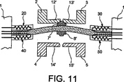
図10は、第1実施形態と同様のデュアルマイクロスイッチであって、コンタクトが最適化されているような実施形態を示す平面図である。マイクロスイッチは、図10においては、起動前の初期状態でもって図示されている。図1と同じ符号を使用することによって、同じ部材を表している。 FIG. 10 is a plan view showing a dual micro switch similar to the first embodiment, in which the contacts are optimized. The microswitch is illustrated in FIG. 10 with an initial state before activation. By using the same reference numerals as in FIG. 1, the same members are represented.
図10においては、導電トラック2,3,4,5の各端部12’,13’,14’,15’が、コンタクトパッド7’,8’に対してより良好な電気的コンタクトを行い得るように最適化されていることに注意されたい。すなわち、コンタクトパッド7’,8’の形状は、先端側と比較して、基端側(つまり、梁に近い方)の方が、より幅の広いものとされている。よって、コンタクトパッド7’,8’は、嵌め込みグルーブが形成されている端部12’,13’,14’,15’の間に、より容易に嵌め込むことができる。
In FIG. 10, the ends 12 ', 13', 14 ', 15' of the
また、導電トラックの端部は、わずかにフレキシブルなものとすることができる。これにより、コンタクトパッドの形状に対する適合性を向上させることができ、したがって、より良好な電気的コンタクトをもたらすことができる。このような状況は、図11に示されている。図11においては、マイクロスイッチは、第1安定状態で示されている。 Also, the end of the conductive track can be slightly flexible. This can improve the conformity to the shape of the contact pad and thus provide better electrical contact. Such a situation is illustrated in FIG. In FIG. 11, the microswitch is shown in the first stable state.
本発明によるマイクロスイッチは、以下のような様々な利点を有している。 The microswitch according to the present invention has various advantages as follows.
本発明によるマイクロスイッチの動作に際しては、双安定性であることに基づいて、小さな電力消費量しか必要としない。 The operation of the microswitch according to the invention requires only a small amount of power consumption based on its bistable nature.
加熱アクチュエータを備えた実施形態は、大きな駆動効率を有している。本発明によるマイクロスイッチにおいては、梁のスイッチングを引き起こすに際して温度を非常に急激に上昇させる必要がないことにより、スイッチング時間が短い。また、本発明によるマイクロスイッチは、静電アクチュエータが加熱アクチュエータに対して組み合わされている場合には、小さなスイッチング電圧を有している。これは、以下の理由に基づくものである。
−熱的バイメタル効果を使用していること。
−加熱用電気抵抗部材が、梁内に組み込まれているとともに、大きな熱膨張係数を有したバイメタル(金属ブロック)部分上に(あるいは、その近傍に)配置されていること。これにより、電気加熱効果を最大限のものとすることができる(最小の熱損失。
−熱伝導度の小さな誘電性梁を使用していること。これにより、バイメタル領域の外部に対しての熱放散を大幅に防止することができる。
Embodiments with heating actuators have great drive efficiency. In the microswitch according to the invention, the switching time is short because it is not necessary to raise the temperature very rapidly when causing the switching of the beam. Also, the microswitch according to the invention has a small switching voltage when the electrostatic actuator is combined with the heating actuator. This is based on the following reason.
-The thermal bimetal effect is used.
-The heating electric resistance member is incorporated in the beam and disposed on (or in the vicinity of) a bimetal (metal block) portion having a large coefficient of thermal expansion. This can maximize the electrical heating effect (minimum heat loss.
-Dielectric beams with low thermal conductivity are used. Thereby, heat dissipation to the outside of the bimetal region can be largely prevented.
したがって、本発明においては、2つの材料間の熱膨張度合いの差と、バイメタルのところにおける加熱用電気抵抗部材による温度の印加および調節と、の双方を使用している。 Therefore, in the present invention, both the difference in the degree of thermal expansion between the two materials and the application and adjustment of the temperature by the heating electric resistance member at the bimetal are used.
本発明においては、デュアルスイッチを得ることができる。 In the present invention, a dual switch can be obtained.
本発明においては、
−コンタクトパッドに対して付与し得る形状によって、および、スイッチング対象をなすトラックの端部に対して付与し得る形状によって、および、付加的には、コンタクトパッドとトラックとの間のコンタクトをより『適切な』ものとし得るよう、コンタクト領域に対して付与されたフレキシブルさによって、
−より小さな電圧でもって電極端子がコンタクトパッドに対してより大きな押圧力を印加し得るよう、適切な形状とされた『補助』電極を付加することによって、
コンタクト抵抗値を最適化し得るスイッチを得ることができる。
In the present invention,
-By the shape that can be applied to the contact pad and by the shape that can be applied to the end of the track to be switched, and in addition, the contact between the contact pad and the track is more Depending on the flexibility given to the contact area,
-By adding an appropriately shaped "auxiliary" electrode so that the electrode terminal can apply a greater pressing force against the contact pad with a lower voltage;
A switch that can optimize the contact resistance value can be obtained.
本発明によるマイクロスイッチの形成は、集積回路の製造方法に対して、大いなる互換性を有している(必要に応じて、『金』による金属化を、製造方法の最終ステップとして行うこと)。 The formation of the microswitch according to the present invention has great compatibility with the integrated circuit manufacturing method (if necessary, metallization with "gold" is performed as the final step of the manufacturing method).
マイクロスイッチの双安定性は、2つの理由により、完全に制御される。第1の理由は、双安定性が、梁が圧縮応力を受けなければならないことによって得られているということである。この応力は、スイッチに構成する材料によってもたらされる(形状、厚さ)。梁が、完全に対称なものとして構成されている場合には、なおかつ、2組をなすアクチュエータの各組が、同じ成膜によって形成されている場合には、応力は、完全に対称なものとなる(アクチュエータの同じ形状および同じ厚さおよび対称性)。この結果、デバイスにとって、ある安定状態と他の安定状態とが同等なものとなる。第2の理由は、圧縮応力の値を、成膜のタイプによって、および、構成によって、および、応力解放『スプリング』の追加によって、制御し得ることである。 The bistability of the microswitch is fully controlled for two reasons. The first reason is that bistability is obtained because the beam must be subjected to compressive stress. This stress is brought about by the material constituting the switch (shape, thickness). If the beam is configured to be completely symmetric, and if each of the two sets of actuators is formed by the same film formation, the stress is assumed to be completely symmetric. (Same actuator shape and same thickness and symmetry). As a result, certain stable states and other stable states are equivalent for the device. The second reason is that the value of compressive stress can be controlled by the type of deposition, by configuration, and by the addition of stress relief “springs”.
本発明によるマイクロスイッチは、有利には、シリコン基板上に形成することができる。埋設領域および梁は、Si3N4あるいはSiO2 あるいは多結晶シリコンから、形成することができる。導電トラック、コンタクトパッド、電極、および、加熱アクチュエータは、金や、アルミニウムや、銅や、ニッケルや、真空中で成膜可能な材料や、電気化学的に成膜(電解、自己触媒メッキ)可能な材料、から形成することができる。加熱用の電気抵抗部材は、TaNや、TiNや、あるいは、Ti、から形成することができる。 The microswitch according to the invention can advantageously be formed on a silicon substrate. The buried region and the beam can be formed from Si 3 N 4, SiO 2 or polycrystalline silicon. Conductive tracks, contact pads, electrodes, and heating actuators are gold, aluminum, copper, nickel, materials that can be deposited in vacuum, and electrochemical deposition (electrolysis, self-catalytic plating) Can be formed from any material. The electric resistance member for heating can be formed from TaN, TiN, or Ti.
例えば、シリコン基板上において、加熱アクチュエータを備えたオーミックマイクロスイッチを形成するための方法においては、以下のような各ステップを行うことができる。
−基板上に、PECVDによって、1μm厚さの酸化物層を成膜し、
−リソグラフィーとエッチングとを行うことにより、埋設領域のためのキャビティを形成し、
−犠牲層として作用することとなる1μm厚さのポリイミド層を成膜し、
−犠牲層に対して、乾式平坦化操作または化学的機械的研磨(CMP)操作を施し、
−3μm厚さのSiO2 層を成膜し、
−このSiO2 層をエッチングすることによって、アクチュエータとコンタクトパッドと導電トラックとのための開口を形成し、
−3μm厚さのアルミナ層を成膜し、
−SiO2 層が露出されるまで、アルミナ層を、CMP操作によって平坦化し、
−0.15μm厚さのSiO2 層を成膜し、
−0.2μm厚さのTiN層を成膜し、
−リソグラフィーとエッチングとを行うことにより、TiN層の中に加熱用電気抵抗部材を形成し、
−0.2μm厚さのSiO2 層を成膜し、
−このSiO2 層に対してリソグラフィーとエッチングとを行うことにより、加熱用電気抵抗部材のコンタクトパッドを形成し、
−犠牲層を停止層として使用することによって、SiO2 層に対してリソグラフィーとエッチングとを行うことにより、梁を形成し、
−Cr/Auからなる0.3μm厚さの2層を成膜し、
−リソグラフィーとエッチングとを行うことにより、導電トラックおよびコンタクトパッドを形成し、
−犠牲層をエッチングすることによって、梁を露出させる。
For example, in the method for forming an ohmic microswitch having a heating actuator on a silicon substrate, the following steps can be performed.
-Depositing a 1 μm thick oxide layer on the substrate by PECVD;
-Forming a cavity for the buried region by performing lithography and etching;
-Depositing a 1 μm thick polyimide layer that will act as a sacrificial layer;
The sacrificial layer is subjected to a dry planarization operation or a chemical mechanical polishing (CMP) operation;
-3 μm thick SiO 2 layer was formed,
- by etching the SiO 2 layer to form an opening for the actuator and the contact pads and conductive tracks,
-3 μm thick alumina layer was formed,
The alumina layer is planarized by a CMP operation until the SiO 2 layer is exposed,
−0.15 μm thick SiO 2 layer was formed,
A TiN layer having a thickness of −0.2 μm was formed;
-Forming an electrical resistance member for heating in the TiN layer by performing lithography and etching;
A -0.2 μm thick SiO 2 layer was deposited,
-Lithography and etching are performed on this SiO 2 layer to form a contact pad of an electrical resistance member for heating;
- By using the sacrificial layer as a stop layer, by performing a lithography and etching of the SiO 2 layer, forming a beam,
-Two layers of 0.3 μm thickness made of Cr / Au are formed,
Forming conductive tracks and contact pads by performing lithography and etching;
-Exposing the beam by etching the sacrificial layer.
他の実施形態においては、シリコン基板上において、加熱アクチュエータを備えたオーミックマイクロスイッチを形成するための方法においては、以下のような各ステップを行うことができる。
−基板上に、PECVDによって、1μm厚さの酸化物層を成膜し、
−リソグラフィーとエッチングとを行うことにより、埋設領域のためのキャビティを形成し、
−犠牲層として作用することとなる1μm厚さのポリイミド層を成膜し、
−犠牲層に対して、乾式平坦化操作または化学的機械的研磨(CMP)操作を施し、
−3μm厚さのSiO2 層を成膜し、
−このSiO2 層をエッチングすることによって、アクチュエータのための開口を形成し、
−3μm厚さのアルミナ層を成膜し、
−アクチュエータを、CMP操作によって平坦化し、
−0.2μm厚さのTiN層を成膜し、
−リソグラフィーとエッチングとを行うことにより、TiN層の中に加熱用電気抵抗部材を形成し、
−0.2μm厚さのSiO2 層を成膜し、
−このSiO2 層に対してリソグラフィーとエッチングとを行うことにより、加熱用電気抵抗部材のコンタクトパッドを形成し、
−SiO2 層に対してリソグラフィーと3.2μm深さのエッチングとを行うことにより、梁を形成し、
−Ti/Ni/Auからなる1μm厚さの3層を成膜し、
−リソグラフィーとエッチングとを行うことにより、導電トラックおよびコンタクトパッドを形成し、
−犠牲層をエッチングすることによって、梁を露出させる。
In another embodiment, the following steps can be performed in a method for forming an ohmic microswitch having a heating actuator on a silicon substrate.
-Depositing a 1 μm thick oxide layer on the substrate by PECVD;
-Forming a cavity for the buried region by performing lithography and etching;
-Depositing a 1 μm thick polyimide layer that will act as a sacrificial layer;
The sacrificial layer is subjected to a dry planarization operation or a chemical mechanical polishing (CMP) operation;
-3 μm thick SiO 2 layer was formed,
- by etching the SiO 2 layer to form an opening for the actuator,
-3 μm thick alumina layer was formed,
The actuator is planarized by a CMP operation,
A TiN layer having a thickness of −0.2 μm was formed;
-Forming an electrical resistance member for heating in the TiN layer by performing lithography and etching;
A -0.2 μm thick SiO 2 layer was deposited,
-Lithography and etching are performed on this SiO 2 layer to form a contact pad of an electrical resistance member for heating;
A beam is formed by performing lithography and etching at a depth of 3.2 μm on the SiO 2 layer;
-Three layers of 1 μm thickness made of Ti / Ni / Au are formed,
Forming conductive tracks and contact pads by performing lithography and etching;
-Exposing the beam by etching the sacrificial layer.
1 基板
2 導電トラック
3 導電トラック
4 導電トラック
5 導電トラック
6 梁
7 電気的コンタクトパッド(電気的コンタクト形成手段)
7’ 電気的コンタクトパッド(電気的コンタクト形成手段)
8 電気的コンタクトパッド(電気的コンタクト形成手段)
8’ 電気的コンタクトパッド(電気的コンタクト形成手段)
12 端部
12’ 端部
13 端部
13’ 端部
14 端部
14’ 端部
15 端部
15’ 端部
20 アクチュエータ(駆動手段)
21 ブロック
22 電気抵抗部材
30 アクチュエータ(駆動手段)
40 アクチュエータ(駆動手段)
50 アクチュエータ(駆動手段)
106 梁
111 応力緩和スロット(解放スプリング形成手段)
261 電極(静電力を誘起するための手段)
262 電極(静電力を誘起するための手段)
263 電極(静電力を誘起するための手段)
264 電極(静電力を誘起するための手段)
271 電極(静電力を誘起するための手段)
272 電極(静電力を誘起するための手段)
273 電極(静電力を誘起するための手段)
274 電極(静電力を誘起するための手段)
302 導電トラック
303 導電トラック
506 梁(静電力を誘起するための手段)
571 電極(静電力を誘起するための手段)
572 電極(静電力を誘起するための手段)
573 電極(静電力を誘起するための手段)
574 電極(静電力を誘起するための手段)
DESCRIPTION OF SYMBOLS 1 Board | substrate 2 Conductive track 3
7 'Electrical contact pad (electrical contact forming means)
8 Electrical contact pads (electrical contact forming means)
8 'Electrical contact pad (electrical contact forming means)
12 end 12 '
21
40 Actuator (drive means)
50 Actuator (drive means)
106
261 electrode (means for inducing electrostatic force)
262 electrode (means for inducing electrostatic force)
263 electrode (means for inducing electrostatic force)
H.264 electrode (means for inducing electrostatic force)
271 Electrode (Means for inducing electrostatic force)
272 electrode (means for inducing electrostatic force)
273 electrode (means for inducing electrostatic force)
274 electrodes (means for inducing electrostatic forces)
302
571 electrode (means for inducing electrostatic force)
572 electrodes (means for inducing electrostatic forces)
573 electrode (means for inducing electrostatic force)
574 electrode (means for inducing electrostatic force)
Claims (15)
少なくとも2つの導電トラック(2,3,4,5)の端部(12,13,14,15)どうしを電気的に接続し得るものであり、
前記マイクロスイッチが、前記基板の表面上に懸架された梁(6)を具備し、
この梁が、両端部のところにおいて埋設されているとともに、非変形状態においては圧縮応力を受けるものとされ、
前記梁(6)が、電気的コンタクト形成手段(7,8)を備え、
これら電気的コンタクト形成手段(7,8)が、前記基板表面に対して平行に前記梁が変形した際には、前記2つの導電トラックの前記端部に対して側方から接触し得るようにして、配置され、
前記マイクロスイッチが、前記梁を駆動するための駆動手段(20,30,40,50)を具備し、
これら駆動手段(20,30,40,50)が、前記梁を、第1安定状態に対応した第1変形位置へと、または、第2安定状態に対応した第2変形位置へと、配置し、
ここで、前記第1変形位置と前記第2変形位置とが、前記非変形状態を挟んで、互いに反対側に位置するものとされ、
前記電気的コンタクト形成手段(7,8)が、前記梁が前記いずれかの変形位置とされた際には、前記2つの導電トラック(2,3,4,5)の前記端部(12,13,14,15)を確実に接続し、
前記梁の前記非変形状態が、前記梁の初期状態である、すなわち、前記マイクロスイッチの起動前の初期状態であることを特徴とするマイクロスイッチ。A bistable MEMS microswitch formed on a substrate (1),
The ends (12, 13, 14, 15) of at least two conductive tracks (2, 3, 4, 5) can be electrically connected to each other,
The microswitch comprises a beam (6) suspended on the surface of the substrate;
This beam is embedded at both ends, and in a non-deformed state it is subjected to compressive stress,
Said beam (6) comprises electrical contact forming means (7, 8);
These electrical contact forming means (7, 8) can contact the ends of the two conductive tracks from the side when the beam is deformed parallel to the substrate surface. Placed,
The microswitch comprises driving means (20, 30, 40, 50) for driving the beam;
These driving means (20, 30, 40, 50) arrange the beam to the first deformation position corresponding to the first stable state or to the second deformation position corresponding to the second stable state. ,
Here, the first deformation position and the second deformation position are located on opposite sides of the non-deformation state,
When the electric contact forming means (7, 8) is in the deformed position of the beam, the end portions (12, 8) of the two conductive tracks (2, 3, 4, 5) are used. 13, 14, 15) are securely connected ,
The microswitch according to claim 1, wherein the non-deformed state of the beam is an initial state of the beam, that is, an initial state before activation of the microswitch.
前記マイクロスイッチが、デュアルマイクロスイッチとされ、
前記第1変形位置においては、第1組をなす2つの導電トラック(2,3)の各端部(12,13)を接続し、
前記第2変形位置においては、第2組をなす2つの導電トラック(4,5)の各端部(14,15)を接続することを特徴とするマイクロスイッチ。The microswitch according to claim 1, wherein
The micro switch is a dual micro switch,
In the first deformation position, the ends (12, 13) of the two conductive tracks (2, 3) forming the first set are connected,
In the second deformed position, each end (14, 15) of the two conductive tracks (4, 5) forming the second set is connected.
前記マイクロスイッチが、シングルマイクロスイッチとされ、
前記第1変形位置においては、2つの導電トラック(302,303)の各端部を接続し、
前記第2変形位置においては、接続をもたらさないことを特徴とするマイクロスイッチ。The microswitch according to claim 1, wherein
The micro switch is a single micro switch,
In the first deformation position, the ends of the two conductive tracks (302, 303) are connected,
A microswitch characterized in that no connection is made in the second deformation position.
前記梁(6)が、誘電性材料あるいは半導体材料から形成され、
前記電気的コンタクト形成手段が、前記梁と一体化された導電性パッド(7,8)から形成されていることを特徴とするマイクロスイッチ。The microswitch according to any one of claims 1 to 3,
The beam (6) is formed of a dielectric material or a semiconductor material;
The microswitch characterized in that the electrical contact forming means is formed of conductive pads (7, 8) integrated with the beam.
前記駆動手段が、バイメタル効果を使用した加熱アクチュエータ(20,30,40,50)を備えていることを特徴とするマイクロスイッチ。The microswitch according to claim 4, wherein
The microswitch characterized in that the driving means includes a heating actuator (20, 30, 40, 50) using a bimetal effect.
前記各加熱アクチュエータ(20)が、熱伝導性材料からなるブロック(21)と、このブロックに対して緊密に接触して配置された電気抵抗部材(22)と、を備えていることを特徴とするマイクロスイッチ。The microswitch according to claim 5, wherein
Each of the heating actuators (20) includes a block (21) made of a heat conductive material and an electric resistance member (22) disposed in close contact with the block. Micro switch to be used.
前記駆動手段が、静電力を誘起するための手段(271,272,273,274; 261,262,263,264)を備えていることを特徴とするマイクロスイッチ。The microswitch according to claim 4, wherein
The microswitch characterized in that the driving means includes means (271, 272, 273, 274; 261, 262, 263, 264) for inducing an electrostatic force.
前記駆動手段が、バイメタル効果を使用した加熱アクチュエータと、静電力を誘起するための手段と、を備えていることを特徴とするマイクロスイッチ。The microswitch according to claim 4, wherein
The microswitch characterized in that the driving means includes a heating actuator using a bimetal effect and a means for inducing an electrostatic force.
前記梁(506)が、導電性材料から形成されていることを特徴とするマイクロスイッチ。The microswitch according to any one of claims 1 to 3,
The microswitch, wherein the beam (506) is made of a conductive material.
前記駆動手段が、静電力を誘起するための手段(506;571,572,573,574)を備えていることを特徴とするマイクロスイッチ。The microswitch according to claim 9, wherein
The microswitch characterized in that the driving means includes means (506; 571, 572, 573, 574) for inducing an electrostatic force.
前記電気的コンタクト形成手段(7’,8’)が、接続すべき前記導電トラック(2,3,4,5)の前記端部(12’,13’,14’,15’)間に嵌め込まれ得るような形状を有していることを特徴とするマイクロスイッチ。The microswitch according to any one of claims 1 to 10, wherein
The electrical contact forming means (7 ′, 8 ′) is fitted between the ends (12 ′, 13 ′, 14 ′, 15 ′) of the conductive tracks (2, 3, 4, 5) to be connected. A microswitch characterized by having such a shape.
前記導電トラック(2,3,4,5)の前記端部(12’,13’,14’,15’)が、接続時に前記電気的コンタクト形成手段(7’,8’)の形状に適合することを可能とし得るよう、フレキシブルさを有していることを特徴とするマイクロスイッチ。The microswitch according to claim 10, wherein
The ends (12 ′, 13 ′, 14 ′, 15 ′) of the conductive tracks (2, 3, 4, 5) conform to the shape of the electrical contact forming means (7 ′, 8 ′) when connected. A microswitch characterized by having flexibility so that it can be performed.
前記梁(106)の埋設された少なくとも1つの端部のための応力緩和スロット(111)を備えていることを特徴とするマイクロスイッチ。The microswitch according to any one of claims 1 to 12,
A microswitch comprising a stress relief slot (111) for at least one end embedded in said beam (106).
前記電気的コンタクト形成手段が、オーミックコンタクトをもたらし得る手段とされていることを特徴とするマイクロスイッチ。The microswitch according to any one of claims 1 to 13,
The microswitch, wherein the electrical contact forming means is a means capable of providing an ohmic contact.
前記電気的コンタクト形成手段が、容量性コンタクトをもたらし得る手段とされていることを特徴とするマイクロスイッチ。The microswitch according to any one of claims 1 to 13,
A microswitch characterized in that the electrical contact forming means is a means capable of providing a capacitive contact.
Applications Claiming Priority (2)
| Application Number | Priority Date | Filing Date | Title |
|---|---|---|---|
| FR0350278A FR2857153B1 (en) | 2003-07-01 | 2003-07-01 | BISTABLE MICRO-SWITCH WITH LOW CONSUMPTION. |
| PCT/FR2004/050298 WO2005006364A1 (en) | 2003-07-01 | 2004-06-30 | Low power consumption bistable microswitch |
Publications (2)
| Publication Number | Publication Date |
|---|---|
| JP2007516560A JP2007516560A (en) | 2007-06-21 |
| JP4464397B2 true JP4464397B2 (en) | 2010-05-19 |
Family
ID=33523072
Family Applications (1)
| Application Number | Title | Priority Date | Filing Date |
|---|---|---|---|
| JP2006516357A Expired - Lifetime JP4464397B2 (en) | 2003-07-01 | 2004-06-30 | Bistable microswitch with low power consumption |
Country Status (7)
| Country | Link |
|---|---|
| US (1) | US7489228B2 (en) |
| EP (1) | EP1639613B1 (en) |
| JP (1) | JP4464397B2 (en) |
| AT (1) | ATE369612T1 (en) |
| DE (1) | DE602004008075T2 (en) |
| FR (1) | FR2857153B1 (en) |
| WO (1) | WO2005006364A1 (en) |
Families Citing this family (73)
| Publication number | Priority date | Publication date | Assignee | Title |
|---|---|---|---|---|
| US7123216B1 (en) | 1994-05-05 | 2006-10-17 | Idc, Llc | Photonic MEMS and structures |
| WO1999052006A2 (en) | 1998-04-08 | 1999-10-14 | Etalon, Inc. | Interferometric modulation of radiation |
| US7532377B2 (en) | 1998-04-08 | 2009-05-12 | Idc, Llc | Movable micro-electromechanical device |
| US8928967B2 (en) | 1998-04-08 | 2015-01-06 | Qualcomm Mems Technologies, Inc. | Method and device for modulating light |
| WO2003007049A1 (en) | 1999-10-05 | 2003-01-23 | Iridigm Display Corporation | Photonic mems and structures |
| TW200413810A (en) | 2003-01-29 | 2004-08-01 | Prime View Int Co Ltd | Light interference display panel and its manufacturing method |
| FR2865724A1 (en) * | 2004-02-04 | 2005-08-05 | St Microelectronics Sa | Micro-electromechanical system for e.g. aerospace field, has beam that is switched between open and closed positions to establish and break contact between two conductors, where positions correspond to beams` buckling positions |
| US7476327B2 (en) | 2004-05-04 | 2009-01-13 | Idc, Llc | Method of manufacture for microelectromechanical devices |
| US20050269688A1 (en) * | 2004-06-03 | 2005-12-08 | Lior Shiv | Microelectromechanical systems (MEMS) devices integrated in a hermetically sealed package |
| KR101354520B1 (en) | 2004-07-29 | 2014-01-21 | 퀄컴 엠이엠에스 테크놀로지스, 인크. | System and method for micro-electromechanical operating of an interferometric modulator |
| US8008736B2 (en) | 2004-09-27 | 2011-08-30 | Qualcomm Mems Technologies, Inc. | Analog interferometric modulator device |
| US7304784B2 (en) | 2004-09-27 | 2007-12-04 | Idc, Llc | Reflective display device having viewable display on both sides |
| US7612932B2 (en) | 2004-09-27 | 2009-11-03 | Idc, Llc | Microelectromechanical device with optical function separated from mechanical and electrical function |
| US7327510B2 (en) | 2004-09-27 | 2008-02-05 | Idc, Llc | Process for modifying offset voltage characteristics of an interferometric modulator |
| US7420725B2 (en) | 2004-09-27 | 2008-09-02 | Idc, Llc | Device having a conductive light absorbing mask and method for fabricating same |
| US7372613B2 (en) | 2004-09-27 | 2008-05-13 | Idc, Llc | Method and device for multistate interferometric light modulation |
| US7289259B2 (en) | 2004-09-27 | 2007-10-30 | Idc, Llc | Conductive bus structure for interferometric modulator array |
| US7527995B2 (en) | 2004-09-27 | 2009-05-05 | Qualcomm Mems Technologies, Inc. | Method of making prestructure for MEMS systems |
| US7564612B2 (en) | 2004-09-27 | 2009-07-21 | Idc, Llc | Photonic MEMS and structures |
| US7554714B2 (en) | 2004-09-27 | 2009-06-30 | Idc, Llc | Device and method for manipulation of thermal response in a modulator |
| US7944599B2 (en) | 2004-09-27 | 2011-05-17 | Qualcomm Mems Technologies, Inc. | Electromechanical device with optical function separated from mechanical and electrical function |
| US7321456B2 (en) | 2004-09-27 | 2008-01-22 | Idc, Llc | Method and device for corner interferometric modulation |
| US7446927B2 (en) * | 2004-09-27 | 2008-11-04 | Idc, Llc | MEMS switch with set and latch electrodes |
| US7724993B2 (en) * | 2004-09-27 | 2010-05-25 | Qualcomm Mems Technologies, Inc. | MEMS switches with deforming membranes |
| US7893919B2 (en) | 2004-09-27 | 2011-02-22 | Qualcomm Mems Technologies, Inc. | Display region architectures |
| US7630119B2 (en) | 2004-09-27 | 2009-12-08 | Qualcomm Mems Technologies, Inc. | Apparatus and method for reducing slippage between structures in an interferometric modulator |
| US7936497B2 (en) | 2004-09-27 | 2011-05-03 | Qualcomm Mems Technologies, Inc. | MEMS device having deformable membrane characterized by mechanical persistence |
| US7302157B2 (en) | 2004-09-27 | 2007-11-27 | Idc, Llc | System and method for multi-level brightness in interferometric modulation |
| US7719500B2 (en) | 2004-09-27 | 2010-05-18 | Qualcomm Mems Technologies, Inc. | Reflective display pixels arranged in non-rectangular arrays |
| US7283030B2 (en) * | 2004-11-22 | 2007-10-16 | Eastman Kodak Company | Doubly-anchored thermal actuator having varying flexural rigidity |
| US7339454B1 (en) * | 2005-04-11 | 2008-03-04 | Sandia Corporation | Tensile-stressed microelectromechanical apparatus and microelectromechanical relay formed therefrom |
| US7460292B2 (en) | 2005-06-03 | 2008-12-02 | Qualcomm Mems Technologies, Inc. | Interferometric modulator with internal polarization and drive method |
| EP2495212A3 (en) | 2005-07-22 | 2012-10-31 | QUALCOMM MEMS Technologies, Inc. | Mems devices having support structures and methods of fabricating the same |
| BRPI0612997A2 (en) | 2005-07-22 | 2010-12-14 | Qualcomm Inc | MEM devices and their manufacturing methods |
| US7630114B2 (en) | 2005-10-28 | 2009-12-08 | Idc, Llc | Diffusion barrier layer for MEMS devices |
| US7916980B2 (en) | 2006-01-13 | 2011-03-29 | Qualcomm Mems Technologies, Inc. | Interconnect structure for MEMS device |
| US7550810B2 (en) | 2006-02-23 | 2009-06-23 | Qualcomm Mems Technologies, Inc. | MEMS device having a layer movable at asymmetric rates |
| US7623287B2 (en) | 2006-04-19 | 2009-11-24 | Qualcomm Mems Technologies, Inc. | Non-planar surface structures and process for microelectromechanical systems |
| US7417784B2 (en) | 2006-04-19 | 2008-08-26 | Qualcomm Mems Technologies, Inc. | Microelectromechanical device and method utilizing a porous surface |
| US7649671B2 (en) | 2006-06-01 | 2010-01-19 | Qualcomm Mems Technologies, Inc. | Analog interferometric modulator device with electrostatic actuation and release |
| US7471442B2 (en) | 2006-06-15 | 2008-12-30 | Qualcomm Mems Technologies, Inc. | Method and apparatus for low range bit depth enhancements for MEMS display architectures |
| US7835061B2 (en) | 2006-06-28 | 2010-11-16 | Qualcomm Mems Technologies, Inc. | Support structures for free-standing electromechanical devices |
| US7385744B2 (en) | 2006-06-28 | 2008-06-10 | Qualcomm Mems Technologies, Inc. | Support structure for free-standing MEMS device and methods for forming the same |
| US7527998B2 (en) | 2006-06-30 | 2009-05-05 | Qualcomm Mems Technologies, Inc. | Method of manufacturing MEMS devices providing air gap control |
| US7545552B2 (en) | 2006-10-19 | 2009-06-09 | Qualcomm Mems Technologies, Inc. | Sacrificial spacer process and resultant structure for MEMS support structure |
| US7684106B2 (en) | 2006-11-02 | 2010-03-23 | Qualcomm Mems Technologies, Inc. | Compatible MEMS switch architecture |
| US7724417B2 (en) * | 2006-12-19 | 2010-05-25 | Qualcomm Mems Technologies, Inc. | MEMS switches with deforming membranes |
| FR2911448B1 (en) * | 2007-01-16 | 2009-07-10 | St Microelectronics Sa | ACOUSTIC RESONATOR IN VOLUME WITH ADJUSTABLE RESONANCE FREQUENCY AND USE OF SUCH RESONATOR IN THE FIELD OF TELEPHONY |
| US7719752B2 (en) | 2007-05-11 | 2010-05-18 | Qualcomm Mems Technologies, Inc. | MEMS structures, methods of fabricating MEMS components on separate substrates and assembly of same |
| US7625825B2 (en) | 2007-06-14 | 2009-12-01 | Qualcomm Mems Technologies, Inc. | Method of patterning mechanical layer for MEMS structures |
| US7630121B2 (en) | 2007-07-02 | 2009-12-08 | Qualcomm Mems Technologies, Inc. | Electromechanical device with optical function separated from mechanical and electrical function |
| US8022896B2 (en) * | 2007-08-08 | 2011-09-20 | Qualcomm Mems Technologies, Inc. | ESD protection for MEMS display panels |
| JP2009077479A (en) * | 2007-09-19 | 2009-04-09 | Japan Radio Co Ltd | Wireless switch control device |
| US20090146773A1 (en) * | 2007-12-07 | 2009-06-11 | Honeywell International Inc. | Lateral snap acting mems micro switch |
| US7642135B2 (en) * | 2007-12-17 | 2010-01-05 | Skyworks Solutions, Inc. | Thermal mechanical flip chip die bonding |
| US8232858B1 (en) * | 2008-02-20 | 2012-07-31 | Sandia Corporation | Microelectromechanical (MEM) thermal actuator |
| US7944604B2 (en) | 2008-03-07 | 2011-05-17 | Qualcomm Mems Technologies, Inc. | Interferometric modulator in transmission mode |
| DE102009018744A1 (en) | 2009-04-27 | 2010-10-28 | Stock E.K. Bernd | Device for mechanical fixing of objects, has base plate, two standing plates and two pivot plates, where plates are movably connected to each other by five hinges |
| US8582254B2 (en) | 2009-05-29 | 2013-11-12 | General Electric Company | Switching array having circuitry to adjust a temporal distribution of a gating signal applied to the array |
| US8427792B2 (en) | 2009-05-29 | 2013-04-23 | General Electric Company | Method and system to enhance reliability of switch array |
| JP5263203B2 (en) * | 2010-03-12 | 2013-08-14 | オムロン株式会社 | Electrostatic relay |
| US8339787B2 (en) * | 2010-09-08 | 2012-12-25 | Apple Inc. | Heat valve for thermal management in a mobile communications device |
| CN102142338A (en) * | 2010-12-16 | 2011-08-03 | 上海交通大学 | Multidirectional and multistable multi-channel micro-electromechanical switch for in-plane movement |
| US8963159B2 (en) | 2011-04-04 | 2015-02-24 | Qualcomm Mems Technologies, Inc. | Pixel via and methods of forming the same |
| US9134527B2 (en) | 2011-04-04 | 2015-09-15 | Qualcomm Mems Technologies, Inc. | Pixel via and methods of forming the same |
| US8659816B2 (en) | 2011-04-25 | 2014-02-25 | Qualcomm Mems Technologies, Inc. | Mechanical layer and methods of making the same |
| FR2984008B1 (en) * | 2011-12-13 | 2014-01-10 | Commissariat Energie Atomique | ELECTRONIC DEVICE |
| FR2990320B1 (en) | 2012-05-07 | 2014-06-06 | Commissariat Energie Atomique | DIGITAL SPEAKER WITH IMPROVED PERFORMANCE |
| ITTO20120691A1 (en) * | 2012-08-01 | 2014-02-02 | Milano Politecnico | IMPACT SENSOR WITH BISTABLE MECHANISM AND METHOD FOR DETECTING IMPACTS |
| FR3012671B1 (en) * | 2013-10-29 | 2015-11-13 | St Microelectronics Rousset | INTEGRATED MECHANICAL DEVICE WITH VERTICAL MOVEMENT |
| WO2017082985A2 (en) * | 2015-08-20 | 2017-05-18 | Northeaslem University | Zero power plasmonic microelectromechanical device |
| KR101968644B1 (en) * | 2018-05-15 | 2019-08-13 | 울산과학기술원 | A bistable structure of twist type manufactured in a 3D printing and use thereof |
| KR101968650B1 (en) * | 2018-05-15 | 2019-04-12 | 울산과학기술원 | Rotationable bistable structure manufactured in a 3D printing and use thereof |
Family Cites Families (13)
| Publication number | Priority date | Publication date | Assignee | Title |
|---|---|---|---|---|
| US5619061A (en) * | 1993-07-27 | 1997-04-08 | Texas Instruments Incorporated | Micromechanical microwave switching |
| US5536963A (en) * | 1994-05-11 | 1996-07-16 | Regents Of The University Of Minnesota | Microdevice with ferroelectric for sensing or applying a force |
| FR2772512B1 (en) * | 1997-12-16 | 2004-04-16 | Commissariat Energie Atomique | MICROSYSTEM WITH DEFORMABLE ELEMENT UNDER THE EFFECT OF A THERMAL ACTUATOR |
| US6188301B1 (en) * | 1998-11-13 | 2001-02-13 | General Electric Company | Switching structure and method of fabrication |
| DE19937811C2 (en) * | 1999-08-11 | 2001-07-26 | Bosch Gmbh Robert | Relays, in particular micro relays for forming a circuit |
| US6239685B1 (en) * | 1999-10-14 | 2001-05-29 | International Business Machines Corporation | Bistable micromechanical switches |
| FR2818795B1 (en) * | 2000-12-27 | 2003-12-05 | Commissariat Energie Atomique | MICRO-DEVICE WITH THERMAL ACTUATOR |
| US6911891B2 (en) * | 2001-01-19 | 2005-06-28 | Massachusetts Institute Of Technology | Bistable actuation techniques, mechanisms, and applications |
| SE0101183D0 (en) * | 2001-04-02 | 2001-04-02 | Ericsson Telefon Ab L M | Micro electromechanical switches |
| KR100929601B1 (en) * | 2001-08-20 | 2009-12-03 | 허니웰 인터내셔널 인코포레이티드 | Snap-In Thermal Switch |
| US6621392B1 (en) * | 2002-04-25 | 2003-09-16 | International Business Machines Corporation | Micro electromechanical switch having self-aligned spacers |
| JP3969228B2 (en) * | 2002-07-19 | 2007-09-05 | 松下電工株式会社 | Mechanical deformation detection sensor, acceleration sensor using the same, and pressure sensor |
| US7283030B2 (en) * | 2004-11-22 | 2007-10-16 | Eastman Kodak Company | Doubly-anchored thermal actuator having varying flexural rigidity |
-
2003
- 2003-07-01 FR FR0350278A patent/FR2857153B1/en not_active Expired - Fee Related
-
2004
- 2004-06-30 EP EP04767860A patent/EP1639613B1/en not_active Expired - Lifetime
- 2004-06-30 WO PCT/FR2004/050298 patent/WO2005006364A1/en not_active Ceased
- 2004-06-30 US US10/561,948 patent/US7489228B2/en not_active Expired - Lifetime
- 2004-06-30 AT AT04767860T patent/ATE369612T1/en not_active IP Right Cessation
- 2004-06-30 DE DE602004008075T patent/DE602004008075T2/en not_active Expired - Lifetime
- 2004-06-30 JP JP2006516357A patent/JP4464397B2/en not_active Expired - Lifetime
Also Published As
| Publication number | Publication date |
|---|---|
| EP1639613B1 (en) | 2007-08-08 |
| US20060152328A1 (en) | 2006-07-13 |
| US7489228B2 (en) | 2009-02-10 |
| DE602004008075D1 (en) | 2007-09-20 |
| ATE369612T1 (en) | 2007-08-15 |
| FR2857153A1 (en) | 2005-01-07 |
| DE602004008075T2 (en) | 2008-05-15 |
| JP2007516560A (en) | 2007-06-21 |
| FR2857153B1 (en) | 2005-08-26 |
| EP1639613A1 (en) | 2006-03-29 |
| WO2005006364A1 (en) | 2005-01-20 |
Similar Documents
| Publication | Publication Date | Title |
|---|---|---|
| JP4464397B2 (en) | Bistable microswitch with low power consumption | |
| CN101147223B (en) | RF MEMS switch with flexible and free switching membrane | |
| US6841839B2 (en) | Microrelays and microrelay fabrication and operating methods | |
| JP4418465B2 (en) | Multi-stable microelectromechanical switch switch and manufacturing method thereof | |
| US8810341B2 (en) | Magnetically actuated micro-electro-mechanical capacitor switches in laminate | |
| US6639493B2 (en) | Micro machined RF switches and methods of operating the same | |
| US7215229B2 (en) | Laminated relays with multiple flexible contacts | |
| US7978045B2 (en) | Multi-actuation MEMS switch | |
| US6635837B2 (en) | MEMS micro-relay with coupled electrostatic and electromagnetic actuation | |
| CN101465243B (en) | MEMS microswitch having a dual actuator and shared gate | |
| US7327211B2 (en) | Micro-magnetic latching switches with a three-dimensional solenoid coil | |
| CN101533740A (en) | MEMS microswitch having a conductive mechanical stop | |
| JP2002075156A (en) | Microswitch and manufacturing method therefor | |
| EP2053017A2 (en) | Electrical connection through a substrate to a microelectromechanical devise | |
| US7420447B2 (en) | Latching micro-magnetic switch with improved thermal reliability | |
| US20020196110A1 (en) | Reconfigurable power transistor using latching micromagnetic switches | |
| US7342473B2 (en) | Method and apparatus for reducing cantilever stress in magnetically actuated relays | |
| JP2005536013A (en) | Microfabricated double throw relay with multimorph actuator and electrostatic latch mechanism | |
| Agrawal | A latching MEMS relay for DC and RF applications | |
| JP2005251549A (en) | Microswitch and driving method of microswitch | |
| US20040183633A1 (en) | Laminated electro-mechanical systems | |
| JP2005536014A (en) | Microfabricated relay with multimorph actuator and electrostatic latch mechanism | |
| US20020196112A1 (en) | Electronically switching latching micro-magnetic relay and method of operating same | |
| CN1979714A (en) | switch | |
| KR100636351B1 (en) | Electrostatic force driven RF MEMS switch and its manufacturing method |
Legal Events
| Date | Code | Title | Description |
|---|---|---|---|
| A621 | Written request for application examination |
Free format text: JAPANESE INTERMEDIATE CODE: A621 Effective date: 20070608 |
|
| A131 | Notification of reasons for refusal |
Free format text: JAPANESE INTERMEDIATE CODE: A131 Effective date: 20090707 |
|
| A601 | Written request for extension of time |
Free format text: JAPANESE INTERMEDIATE CODE: A601 Effective date: 20091007 |
|
| A602 | Written permission of extension of time |
Free format text: JAPANESE INTERMEDIATE CODE: A602 Effective date: 20091015 |
|
| A521 | Request for written amendment filed |
Free format text: JAPANESE INTERMEDIATE CODE: A523 Effective date: 20091216 |
|
| TRDD | Decision of grant or rejection written | ||
| A01 | Written decision to grant a patent or to grant a registration (utility model) |
Free format text: JAPANESE INTERMEDIATE CODE: A01 Effective date: 20100119 |
|
| A01 | Written decision to grant a patent or to grant a registration (utility model) |
Free format text: JAPANESE INTERMEDIATE CODE: A01 |
|
| A61 | First payment of annual fees (during grant procedure) |
Free format text: JAPANESE INTERMEDIATE CODE: A61 Effective date: 20100218 |
|
| FPAY | Renewal fee payment (event date is renewal date of database) |
Free format text: PAYMENT UNTIL: 20130226 Year of fee payment: 3 |
|
| R150 | Certificate of patent or registration of utility model |
Ref document number: 4464397 Country of ref document: JP Free format text: JAPANESE INTERMEDIATE CODE: R150 Free format text: JAPANESE INTERMEDIATE CODE: R150 |
|
| FPAY | Renewal fee payment (event date is renewal date of database) |
Free format text: PAYMENT UNTIL: 20140226 Year of fee payment: 4 |
|
| R250 | Receipt of annual fees |
Free format text: JAPANESE INTERMEDIATE CODE: R250 |
|
| R250 | Receipt of annual fees |
Free format text: JAPANESE INTERMEDIATE CODE: R250 |
|
| R250 | Receipt of annual fees |
Free format text: JAPANESE INTERMEDIATE CODE: R250 |
|
| R250 | Receipt of annual fees |
Free format text: JAPANESE INTERMEDIATE CODE: R250 |
|
| R250 | Receipt of annual fees |
Free format text: JAPANESE INTERMEDIATE CODE: R250 |
|
| R250 | Receipt of annual fees |
Free format text: JAPANESE INTERMEDIATE CODE: R250 |
|
| R250 | Receipt of annual fees |
Free format text: JAPANESE INTERMEDIATE CODE: R250 |
|
| R250 | Receipt of annual fees |
Free format text: JAPANESE INTERMEDIATE CODE: R250 |
|
| R250 | Receipt of annual fees |
Free format text: JAPANESE INTERMEDIATE CODE: R250 |
|
| R250 | Receipt of annual fees |
Free format text: JAPANESE INTERMEDIATE CODE: R250 |
|
| R250 | Receipt of annual fees |
Free format text: JAPANESE INTERMEDIATE CODE: R250 |
|
| R250 | Receipt of annual fees |
Free format text: JAPANESE INTERMEDIATE CODE: R250 |
|
| EXPY | Cancellation because of completion of term |