JP4459335B2 - Ferroelectric transistor type nonvolatile memory element and manufacturing method thereof - Google Patents
Ferroelectric transistor type nonvolatile memory element and manufacturing method thereof Download PDFInfo
- Publication number
- JP4459335B2 JP4459335B2 JP29708999A JP29708999A JP4459335B2 JP 4459335 B2 JP4459335 B2 JP 4459335B2 JP 29708999 A JP29708999 A JP 29708999A JP 29708999 A JP29708999 A JP 29708999A JP 4459335 B2 JP4459335 B2 JP 4459335B2
- Authority
- JP
- Japan
- Prior art keywords
- thin film
- ferroelectric
- film
- nonvolatile memory
- insulating
- Prior art date
- Legal status (The legal status is an assumption and is not a legal conclusion. Google has not performed a legal analysis and makes no representation as to the accuracy of the status listed.)
- Expired - Fee Related
Links
Images


Description
【0001】
【発明の属する技術分野】
本発明は、不揮発性記憶素子に関し、特に、強誘電体を用いた不揮発性メモリの強誘電体トランジスタ型不揮発性記憶素子に関するものである。
【0002】
【従来の技術】
最近、開発が進められている強誘電体を使用したFeRAM(Ferroe1ectric Random Access Memory)は、DRAMのキャパシタを強誘電体キャパシタに置き換えた構成をしており(特開平2−113496号公報)、その動作は強誘電体キャパシタの分極が反転するときと、反転しないときの電荷量の差を検知することによって、記憶された情報が「1」であったか、「0」であったかを判断している。このため、情報を読み出す際に保持していた情報が破壊される、いわゆる破壊読出しとなるのは必然である。
【0003】
さらに、この方法においては、分極の反転における電荷を電流として取り出して検出するために、キャパシタの面積が小さくなるとともに、電流値も小さくなり検出が困難になる。このことは、FeRAMのセル構造がスケーリング則に従わないがゆえに発生する基本的な問題である。
【0004】
また、強誘電体キャパシタから排出される電荷量を比較するために、通常、参照セルを各セルに1対ずつ配置する必要があるために、1つのメモリセルを構成するのに、2トランジスタ2キャパシタが必要となる。そのため、メモリセル面積が同加工精度のDRAMに比較して、2倍以上大きくなる問題がある。
【0005】
一方、強誘電体を電界効果型トランジスタ(FET;Field Effect Transistor)のゲート部に配置する強誘電体トランジスタは、単一のトランジスタでメモリセルを構成することが可能である。この素子は、強誘電体の分極がトランジスタのチャネルの電荷を誘起することによって、ソース、ドレイン間をオン、オフさせるもので、セル面積を比例縮小させても、ドレイン電流の変化率は変わらない。これは、強誘電体トランジスタのメモリセルがスケーリング則に従っている(電子情報通信学会誌77-9 p976, 1994)ことを意味し、微細化に際する原理的な限界は存在しない。
【0006】
以上のことは、セル面積を小さくすることに関して有利であるばかりでなく、強誘電体の分極により、FETのオン、オフを維持するため、読み出し動作により情報が破壊されない、いわゆる非破壊読出しすることも可能である。
【0007】
さらに、強誘電体をゲート部分に配置する強誘電体トランジスタには、2つの種類に大別される。その1つはMFIS(Metal-Ferroelectric-Insulator-Semiconductor)構造を持つ強誘電体トランジスタで、強誘電体がその分極によりゲート絶縁膜を介して、半導体基板表面に電荷を誘起するものであり、もう1つは、MFMIS(Metal-Ferroelectric-Metal-Insulator-Semiconductor)構造を持つ強誘電体トランジスタで、MFIS構造の強誘電体層と絶縁層との間に金属電極層を挟み込んだものである。
【0008】
図2は、これらの強誘電体トランジスタの構造を等価回路で表わしたものであるが、この図2から、上部電極25一半導体基板20間に電圧を印加して強誘電体24を分極させるとき、強誘電体の分極が十分飽和するまで、電圧を印加することが、記憶保持特性の観点から必要であるが、CF(強誘電体層の容量)がC1(ゲート絶縁層の容量)に比較して小さくなるように設計することが重要である。この設計を可能にする1つの方法として、強誘電体容量の面積をゲート絶縁層の面積より小さくするすることが考えられるが、このためには、強誘電体容量の下部に等電位面が存在することが必要で、MFMIS構造によって実現される。
【0009】
MFMIS構造を持つ強誘電体トランジスタの従来例(T.Nakamura et. al. Dig.Tech.Pap. of 1995 IEEE Int. Solid-State Circuits Conf. p.68 (1995))では、図12(A)に示すように、半導体基板20上にゲート絶縁酸化膜21と、多結晶膜22と、導電膜23と、強誘電体膜24と、白金等の電極25と順次積層されて、不図示のソース、ドレインをセルフアライン法等により形成し、ソースとドレイン間の上部にゲート電極等を設けた強誘電体メモリセルが提案された。この図12(A)に示すように、ゲート絶縁膜としてシリコン熱酸化膜21と多結晶シリコン22のゲート電極からなるゲート構造を用いている。強誘電体容量とゲート部分を一括して加工すると、側壁におけるリーク電流が大きく実用にならない。
【0010】
このため、シリコン熱酸化膜21と多結晶シリコン22のゲート部分を通常のセルフアライン法にて作製し、このトランジスタの上に層間絶縁膜にあけたコンタクト穴を介して強誘電体容量が接続する構造をとらざるを得ない(図12(B))。図12Bに示すように、強誘電体メモリセルは、半導体基板20上にゲート絶縁酸化膜21と、多結晶シリコン膜22と、コンタクト穴を通して接続した導電膜23と、強誘電体膜24と、白金等の電極25とが順次形成されて、セルフアライン法等により不図示のソース、ドレインを形成し、ソースとドレイン間の上部にゲート電極を設けている。
【0011】
この構造では、トランジスタの多結晶シリコン電極22とコンタクト穴の問に位置合わせ余裕が必要なため、多結晶シリコン電極幅(ゲート長に相当)を最小加工寸法まで短くできない。また、位置合わせ余裕が極めて小さくなると、図12(C)のような不具合が発生し、歩留まりが急激に低下する。このように、MFMIS構造を持つ強誘電体トランジスタは、ゲート長をLSIの製造プロセスの最小加工寸法に設定することができない。
【0012】
また、強誘電体トランジスタは、強誘電体の電流リーク、電荷の注入が起きると、強誘電体の残留分極を相殺する現象が起きるため、記憶保持時間が極端に短くなるという問題を抱えている。特に半導体基板側から電荷注入が起きるとFETのチャネルが消失し、短時間で情報を失う点はより深刻である。半導体基板上に形成されたゲート絶縁膜はきわめて薄い上に、ドライエッチングなどにより加工された端面では、電荷注入やリーク電流が発生しやすいと考えられる。
【0013】
【発明が解決しようとする課題】
上記のように、MFMIS構造の強誘電体トランジスタは、ゲート絶縁膜の面積より強誘電体容量の面積を小さくする必要がある。また、ゲート長をLSI製造プロセスの最小加工寸法まで縮めることができない問題がある。さらに、強誘電体トランジスタは、強誘電体のリーク電流、強誘電体への電荷注入により記憶保持時間が短くなる課題を有している。このリーク電流や電荷の注入は、ダメージを受けたゲート絶縁膜や強誘電体の端面において発生しやすくなると考えられる。
【0014】
本発明は、このような従来の技術が有する未解決の課題を解決するべく行われたものであり、ゲート絶縁膜面積より強誘電体容量の面積を小さくすることを可能にし、ゲート長をLSI製造プロセスの最小加工寸法まで縮めることを可能にし、さらにダメージを受けたゲート絶縁膜や強誘電体の端面におけるリーク電流、電荷の注入を防ぎ、記憶保持上優れた強誘電体トランジスタ型不揮発性メモリ素子を提供するものである。
【0015】
【課題を解決するための手段および作用】
本発明による強誘電体トランジスタ型不揮発性記憶素子は、半導体基板上に形成した電界効果型トランジスタのゲート部として、絶縁性薄膜、第一導電体薄膜、強誘電体薄膜、第二導電体薄膜を順次積層した構造を持つ強誘電体トランジスタ型不揮発性記憶素子において、ソース領域およびドレイン領域を覆うシリコン酸化膜の内縁と前記絶縁性薄膜の外縁とが接合し、かつ前記第一導電体薄膜のチャネル長方向の長さが前記絶縁性薄膜より長く、前記第一導電体薄膜の端面が前記絶縁性薄膜の端面と接触しないように配置され、前記シリコン酸化膜として、前記絶縁性薄膜より膜厚が厚い熱酸化膜が用いられ、前記シリコン酸化膜は、前記絶縁性薄膜をマスクとして用いて前記半導体基板を熱酸化させることにより、前記シリコン酸化膜の内縁が前記絶縁性薄膜の外縁により規定されるように形成され、前記第一導電体薄膜が前記シリコン酸化膜の上面及び前記絶縁性薄膜の上面に沿うように形成されていることを特徴とすることを特徴とする。
【0016】
また、半導体基板上に形成した電界効果型トランジスタのゲート部として、絶縁性薄膜、第一導電体薄膜、強誘電体薄膜、第二導電体薄膜を順次積層した構造を持つ強誘電体トランジスタ型不揮発性記憶素子の製造方法において、半導体基板としてシリコンを主体とする単結晶基板を用い、前記絶縁性薄膜を形成、加工し、前記絶縁性薄膜をマスクとしてソース領域およびドレイン領域を形成し、前記絶縁性薄膜をマスクとして前記半導体基板表面を熱酸化することによって、前記ソース領域およびドレイン領域を覆うシリコン酸化膜を形成する第1形成工程と、前記第1形成工程後に、前記絶縁性薄膜上に第一導電体薄膜を形成し、前記第一導電体薄膜上に金属有機物の強誘電体薄膜を塗布焼成し、次に、第二導電体薄膜を形成する第2形成工程とを有し、前記第2形成工程において形成される前記第一導電体薄膜の外縁が前記シリコン酸化膜上に位置することを特徴とする。
【0017】
本発明の概要を示す図1をもとに、その作用について説明する。半導体基板1の上に形成した電界効果型トランジスタは、一般にゲート絶縁膜5と、導電体電極6の積層構造を持つゲート部を持ち、この導電体電極6に電圧を印加してソース、ドレイン2間に流れる電流を制御し、オン、オフの動作をさせる。
【0018】
本発明のゲート部においては、酸素の拡散を阻止する絶縁性薄膜5をゲート絶縁膜とし、その上に第一導電体薄膜6、強誘電体薄膜7、第二導電体薄膜8を順次積層した構造を持つ強誘電体キャパシタ(容量)を配置し、この強誘電体が発現する残留分極によって、ゲート部に電圧が印加されないときでも、電界効果型トランジスタをオン、オフ状態に固定することができるため、不揮発性メモリとして機能させることができる。
【0019】
ここで、本発明の強誘電体トランジスタ型不揮発性記憶素子の書込み、消去、読み出しの各動作について、図1を参照して説明する。
【0020】
図1において、一例として5V駆動のp型基板を用いたnチャネル型FETの場合について説明する。まず、書込み動作は、第二導電体薄膜8側に5V、基板1側に0Vを印加し、強誘電体薄膜7に下向きの分極を発生させる。この操作により、第二導電体薄膜8側を0Vとしても、ソース2、ドレイン2間が導通するON状態にすることができる。この状態を「1」と定義する。次に、消去動作について説明する。第二導電体薄膜8側に0V、基板1側に5Vを印加し、強誘電体薄膜7に下向きの分極を発生させる。この操作により、第二導電体薄膜側を0Vのときソース2、ドレイン2間が導通しないOFF状態にすることができる。この状態を「0」と定義する。次に、読み出し動作について説明する。第二導電体薄膜8側を0V、基板1側も0Vとした上でソース2を0Vとし、ドレイン2に2Vのパルスを印加する。このメモリセルが「1」か「0」かは、ドレイン電圧が直ちに低下するか否かで判定し、直ちに低下した場合はこのメモリセルがON状態であることを意味し、「1」が記憶されていたことになる。ドレイン電圧が直ちには低下しなかったときは反対に「0」が記憶されていたことになる。こうして、強誘電体の分極方向に応じた不揮発性の記憶素子として動作する。なお、上述の電圧設定は一例であり、基板1側を一定電位として、ゲートに該当する第二導電体薄膜8側をプラス・マイナス電位に振り分けてもよい。
【0021】
本発明による強誘電体トランジスタ型記憶素子において、該酸素の拡散を阻止する絶縁性薄膜より膜厚の厚いソース部およびドレイン部を覆うシリコン酸化膜4を配置し、前述の酸素の拡散を阻止する絶縁性薄膜5の端面とシリコン酸化膜4とが接合するようにし、さらに第一導電体薄膜6のソース、ドレイン方向の長さが酸素の拡散を阻止する絶縁性薄膜5より長くした上で、第一導電体薄膜6の端面が絶縁性薄膜5の端面と接触しないように配置する。このような積層構造をとることにより、ゲート絶縁膜(絶縁性薄膜5)のエッチング工程と第一導電体薄膜6のエッチング工程とを分離した上で、ゲート絶縁膜5とソース、ドレインのセルフアライン法による加工が可能となり、このためにゲート部分の端面(第一導電体薄膜6および強誘電体薄膜7の端面)におけるリーク電流、電荷注入量を大きく抑制することができる。
【0022】
また、ソース、ドレイン部をおおう該酸素の拡散を阻止する絶縁性薄膜5より膜厚の厚いシリコン酸化膜4を用いることにより、ゲート電極6の部分の寄生容量を減少させることができ、高速な動作を可能にする。
【0023】
本発明の場合、絶縁性薄膜を形成、加工後に、該絶縁性薄膜をマスクとしてソース、ドレイン部を形成するために不純物注入を行ない、該絶縁性薄膜に覆われていない部分に膜厚の厚いシリコン酸化膜4を形成する。第一導電体薄膜6は、絶縁性薄膜5上にその端面が膜厚の厚いシリコン酸化膜4上にかかるように形成される。このことによって、絶縁性薄膜(ゲート絶縁膜)5との位置合わせ余裕を確保しながら、ゲート電極に対して実効的にセルフアラインプロセスにて強誘電体トランジスタを作製することができる。
【0024】
本発明における絶縁性薄膜5は、ソース、ドレイン部をおおうシリコン酸化膜4を形成する際のマスクとして利用できるだけでなく、強誘電体を加熱、結晶化する際にゲート絶縁膜の膜厚が増加する不具合を回避することができる。酸素の拡散を阻止する絶縁性薄膜5は、好ましくはSiON膜である。
【0025】
本発明における第一導電体薄膜6および第二導電体薄膜8として、好ましくは白金、イリジウム、酸化イリジウム、またはこれらの混合物、またはこれらの積層構造体を用いる。また、強誘電薄膜7としては、ABO3型、A2B2O7型の構造を持つ強誘電体、または層状ペロブスカイト型構造もつ強誘電体を用いることができる。
【0026】
ここで、A,Bは金属元素を表わす。また、該強誘電薄膜7として、比誘電率50以下のものを用いることにより、記憶保持特性に優れた不揮発性記憶素子を得ることができる。特に、Sr2Ta2O7、あるいはSr2(NbTa)2O7、あるいはSrBi2Ta2O9のように、より比誘電率が低い強誘電体材料を用いることがより好ましい。
【0027】
また、強誘電体容量の有効面積を電界効果型トランジスタのチャネル領域の面積よりも小さくすることがより好ましい。その理由としては、ゲート部分の構造が、図2のように、強誘電体薄膜7とシリコン窒化物を主体とする絶縁性薄膜5が直列に接続されたキャパシタと等価な回路となるため、電圧を印加すると各薄膜に電圧が容量に反比例してかかるため、強誘電体の比誘電率が小さく、容量が小さくなるほうが印加電圧が高くなり、分極を十分飽和させることができ、記憶保持に有利となるからである。
【0028】
また、本発明では、ソース部およびドレイン部を覆う該酸素の拡散を阻止する絶縁性薄膜5より膜厚の厚いシリコン酸化膜4を配置し、前述の酸素の拡散を阻止する絶縁性薄膜5の端面とが接合するように配置するため、ゲート絶縁膜(絶縁性薄膜5)と、第一導電体薄膜6との位置合わせ余裕を大きくとることができるため、ゲート長をリソグラフィーの最小加工寸法まで短くすることができる。
【0029】
さらに、本発明では、該酸素の拡散を阻止する絶縁性薄膜5を加工した後、この絶縁性薄膜5をマスクとして、シリコン基板を熱酸化することによってソース部およびドレイン部をおおうシリコン酸化膜4を形成することができるため、きわめて簡便な方法で素子を製造することができる。
【0030】
ここで、従来より検討された報告との比較を行なう。1998年藤森らが行なった報告(Jpn. Appl. Phys. vol.37 (1998) p.5207)では、Po1y−Si/SiO2/Si積層構造を持つゲート電極上部にPt/STN/IrO2/Pt構造を持つ(STNはSr2(TaNb)2O7をしめす)強誘電体容量を接続する構造をとっている。この場合、Po1y−Si/SiO2構造を形成、加工した後にソース部およびドレイン部をイオン注入により形成し、層間絶縁膜を形成し、強誘電体容量と接合するためのコンタクト穴を明けることになる。このため、リソグラフィーの位置合わせ余裕を見込む必要があり、ゲート電極部のPOly−Si/SiO2構造を最小加工寸法まで小さくすることはできず、デバイス面積が大きくなる難点がある。これに対し、本発明においては、前述のようにこの問題を克服することができる。
【0031】
また、特開平5−135570号公報(発明者、中村孝)の発明では、電界効果型トランジスタのゲート電極端面と、強誘電体容量の電極、および強誘電体の端面が一致するように構成されているが、このような構造では、端面の加工ダメージを受けた部分を通じて、大量のリーク電流や電荷の注入が起こり、記憶保持時間が極端に短くなる。これに対し、本発明においては、リーク電流の削減、電荷の注入を防止し、このような問題を解決できる。
【0032】
また、特開平5−121759号公報(発明者、鮫島克己)の発明では、Po1y−Si/SiO2構造を持つゲート電極を低誘電率の層間絶縁膜に埋め込み、本発明と似た効果を得ることができるが、この構造を実現するためには、犠牲ゲートを用い、ソース、ドレイン部を形成した後、低誘電率層間絶縁膜を形成し、CMP(Chemical Mechanical Polishing)を用いて平坦化した後、犠牲ゲートを取り去った上で、新たにPoly−Si/SiO2積層構造を形成し、再びCMPにて平坦化埋め込みを行なうという、きわめて複雑な製造プロセスを必要とする。本発明では、上記に述べたようなより短い製造工程により、同様の効果を得ることができる。
【0033】
また、特開平11−145411号公報(発明者、中村孝)の発明では、ゲート部分のSiO2ゲートエリア上に、該SiO2の面積より小さな強誘電体キャパシタエリアを形成することを特徴としているが、セルフアラインプロセスにより、ソース部およびドレイン部を形成することが困難であるために、位置合わせ余裕を大きくとる必要があり、素子全体が大きくなる問題がある。また、同公報では、ゲート絶縁膜に酸素の拡散を阻止する材料を使用することを求めておらず、強誘電体の加熱、結晶化工程で、ゲート絶縁膜の膜厚が増加する不具合を回避できない。本発明においては、ゲート絶縁膜の膜厚を薄くでき、このような問題を解決できる。
【0034】
本発明によれば、従来方法では困難であったソース、ドレイン間距離がLSI製造工程の最小加工寸法になっても、位置合わせ余裕を確保できるため、面積の小さい強誘電体トランジスタを製作することができ、さらにゲート絶縁膜の加工と強誘電体薄膜の加工を分離し、かつ強誘電体や電極において、エッチングダメージを受けた端面部分をゲート絶縁膜の端面と引き離すことにが可能となり、強誘電体薄膜におけるリーク電流の低減、強誘電体薄膜への電荷注入の低減に大きな効果を得ることができ、記憶保持時間を大幅に延ばすことができる。
【0035】
さらに、シリコン基板を用いたうえで、シリコン窒化物を主体とする絶縁性薄膜5の形成、加工後にソース、ドレイン部をおおうシリコン酸化膜4をシリコン基板の熱酸化法により形成することによって、工程の簡略化を成すことができるばかりでなく、綴密なシリコン酸化膜4を得ることができる。
【0036】
以上の説明のように、本発明によれば、従来の強誘電体トランジスタでは達成困難な課題を容易な構造、製造方法によって実現することができる。
【0037】
【発明の実施の形態】
以下、本発明の実施形態について、図面を参照しつつ詳細に説明する。
【0038】
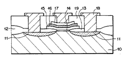
[実施形態1]
まず、図3に示すような、不揮発性記憶素子としての強誘電体トランジスタ(サンプルA)と、比較例として図4に示すような強誘電体トランジスタ(サンブルB)を試作した。双方の強誘電体トランジスタは、p型シリコン(100)単結晶基板10を用い、フィールド酸化膜12を熱酸化法にて成膜、フォトリソグラフィー、エッチングによりトランジスタを作製するべき活性化領域を開口した。
【0039】
図3、図4において、半導体基板10の上に形成した電界効果型トランジスタは、ゲート絶縁膜14と、第一導電体電極15の積層構造を持つゲート部を持ち、この第一導電体電極15は強誘電体薄膜の容量を小さくして、図2に示すCIに対するCFへの印加電圧をある程度稼ぐためのものである。このゲート部14、15においては、酸素の拡散を阻止する絶縁性薄膜をゲート絶縁膜14とし、その上に第一導電体薄膜15、強誘電体薄膜16、第二導電体薄膜17を順次積層した構造を持ち、層間絶縁膜19にホールを設けて電極18を形成する。また、図3、図4共に、概念的には、ゲート部のゲート絶縁膜14を形成した後、ゲート絶縁膜14をマスクとして、ソース・ドレイン領域11をイオン注入法により形成する。また、ソース・ドレイン領域11を形成後、アニールにより熱酸化膜13を形成する。このゲート部上の強誘電体薄膜16が発現する残留分極によって、不揮発性記憶機能を発揮させる電界効果型トランジスタを形成している。
【0040】
また、図3における強誘電体トランジスタ不揮発性記憶素子の動作は、図1の場合と同様であるが、再度説明する。本発明の強誘電体トランジスタ型不揮発性記憶素子の書込み、消去、読み出しの各動作について、図3を参照して説明する。
【0041】
図3において、電圧印加の一例として、5V駆動のp型基板を用いたnチャネル型FETの場合について説明する。まず、書込み動作は、第二導電体薄膜17側に5V、基板10側に0Vを印加し、強誘電体薄膜16に下向きの分極を発生させる。この操作により、第二導電体薄膜17側を0Vとしてもソース11、ドレイン11間が導通するON状態にすることができる。この状態を「1」と定義する。次に、消去動作について説明する。第二導電体薄膜17側に0V、基板10側に5Vを印加し、強誘電体薄膜16に下向きの分極を発生させる。この操作により、第二導電体薄膜17側を0Vのときソース11、ドレイン11間が導通しないOFF状態にすることができる。この状態を「0」と定義する。
【0042】
次に、読み出し動作について説明する。第二導電体薄膜17側を0V、基板10側も0Vとした上でソース11を0Vとし、ドレイン11に2Vのパルスを印加する。このメモリセルが「1」か「0」かは、ドレイン電圧が直ちに低下するか否かで判定し、直ちに低下した場合はこのメモリセルがON状態であることを意味し、「1」が記憶されていたことになる。ドレイン電圧が直ちには低下しなかったときは反対に「0」が記憶されていたことになる。こうして、強誘電体の分極方向に応じた不揮発性の記憶素子として動作する。なお、上述の電圧設定は一例であり、基板10側を一定として、ゲートに該当する第二導電体薄膜17側をプラス・マイナス電位に振り分けてもよい。また、この記憶素子をマトリクス状に配置して、ビット線、ワード線をゲート電極、ドレイン電極等と接続すれば、高集積した不揮発性半導体メモリができあがる。
【0043】
(サンプルAの製造方法)
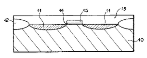
図3に示すサンプルAの場合、まずゲート絶縁膜としてSiON薄膜14を作製する。あらかじめ窒素イオンを活性領域に約20keVのエネルギーでイオン注入し、後に酸素雰囲気中で800℃にてアニールする。これによって、膜厚5nmの絶縁膜が形成できる。次にレジストを塗布した上で、フォトリソグラフィー、ドライエッチングにより、ゲート絶縁膜14の端面部分を加工する。次に、このサンプルに対して、リンイオンをイオン注入し、ソース、ドレイン領域11を形成する。さらに、レジストを剥離後、酸素雰囲気中、約800℃にてアニールすることによって、ソース、ドレイン領域11をおおうようにシリコンの熱酸化膜13を形成することができる。この時の熱酸化膜13の膜厚は、約20nm程度であった。SiON膜は酸素の透過を阻止すため、ゲート領域には酸化膜はほとんど形成しない。800℃の酸素雰囲気中、アニールにより、ソース、ドレイン領域の活性化アニールも兼ねて行なうことができる。この結果、図5に示すような構造となる。
【0044】
次に、ゲート絶縁膜14上に、第一導電体薄膜として、チタンと、白金との積層膜15をスパッタリング法にて形成する。膜厚は白金、チタン合計で約200nmである。次に、強誘電体薄膜として、Sr(NbTa)2O7膜16を金属有機物を塗布焼成する方法によって形成する。膜厚は約300nmである。次に、第二導電体薄膜としてイリジウムをスパッタリング法にて成膜した。膜厚は約150nmである。これを第二導電体薄膜、強誘電体薄膜、第一導電体薄膜の順に、順次フォトリソグラフィー、ドライエッチングによって加工した。さらに、層間絶縁膜19としてプラズマCVD法にてシリコン酸化膜を形成、第二導電体薄膜と、ソース、ドレイン層上にコンタクトホールをあけて、アルミニウム電極18を形成、加工して完成となる。完成した強誘電体トランジスタを上からみた図を、図7に示す。図7において、強誘電体トランジスタ(サンプルA)は、ゲート絶縁膜14と、その上に幅広い第一導電体薄膜の導体積層膜15と、強誘電体16と、第二導電体薄膜のゲート電極17とからゲート部は形成されており、ソース,ドレイン層11と、熱酸化膜13と、ソース、ドレイン電極20とが形成されている。導体積層膜15とゲート電極17と間に形成される強誘電体16の容量の有効面積が、ゲート絶縁膜14の面積の約1/5となるように、強誘電体容量を小さくして、強誘電体膜のゲート絶縁膜14の幅方向の長さをも考慮して設定した。
【0045】
(サンプルBの製造方法)
つぎに、比較例のサンプルBの場合、図4に示すように、まずゲート絶縁膜としてSiON薄膜14を作製する。あらかじめ窒素イオンを活性領域に約20keVのエネルギーでイオン注入し、後に酸素雰囲気中で800℃にてアニールする。これによって、膜厚5nmの絶縁膜14が形成できる。次に第一導電体薄膜として、チタン、白金を順次積層した薄膜15を形成する。次に、強誘電体薄膜として、Sr(NbTa)2O7膜16を金属有機物を塗布焼成する方法によって形成する。膜厚は約300nmである。次に、第二導電体薄膜17としてイリジウムをスパッタリング法にて成膜した。膜厚は約150nmである。さらに、レジストを塗布した上でフォトリソグラフィー、ドライエッチングにより、ゲート積層構造部分を一括して加工する。
【0046】
次に、このサンプルに対して、リンイオンをイオン注入し、ソース、ドレイン領域11を形成する。さらに、窒素雰囲気中約800℃にてアニールすることによってソース、ドレイン領域11を活性化する。この結果、図6に示すような構造となる。図6において、半導体基板10上にゲート絶縁膜14と、金属積層の薄膜15と、強誘電体薄膜16と、第二導電体薄膜17とを形成している。
【0047】
次に、プラズマCVD法により、層間絶縁膜19としてシリコン酸化膜を形成し、コンタクトホールをあけて、アルミニウム電極18を形成、加工して完成となる。
【0048】
サンプルA、およびBについて、第二導電体電極17とシリコン単結晶基板10間に電圧を印加し、電圧一電流特性を測定した。これによりゲート部分のリーク電流を測定することができる。この結果を図8に示す。サンブルAは、3V印加時でも、リーク電流は10-9アンペア/cm2台であるのに対し、サンプルBは、10-6アンペア/cm2台となり、サンプルAの方がリーク電流が小さくなっていることは明らかである。これは、サンプルBがゲート絶縁膜SiON膜14と第一導電体薄膜を一括加工し、かっ端面が一致しているために、エッチングダメージを受けた部分を通じて電流が流れるため、リーク電流が大きくなるものと考えられる。これに対し、サンプルAの場合は、ダメージを受けた端面が一致していないため、リーク経路が遮断され、リーク特性が良好になると考えられる。
【0049】
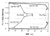
(サンプルAとサンプルBの評価)
次に、記憶保持特性を評価する。サンプルA、およびBについて、第二導電体電極17とシリコン単結晶基板10間に電圧を印加し、強誘電体の分極を発生させて情報を書き込む。その後、ソース部を接地し、ドレイン部に1Vの電圧を印加し、書込み電圧を印加してから、ある時間保持した後のドレインに流れる電流値を観察した。その結果を図9に示す。図中、印加電圧Vgを5Vから0Vに、及び−5Vから0Vとした場合のサンプルA,Bのそれぞれの測定結果である。サンプルA,Bともに時間106secの経過時間で測定した。この結果から明らかなように、サンプルAの方がサンプルBに比べて、記憶保持時間が長くなっていることが判る。これは、強誘電体に流れ込む電荷量を大きく抑制できたことによると考えられる。
【0050】
[実施形態2]
本発明の実施形態2による強誘電体トランジスタ型不揮発性記憶素子について、説明する。
【0051】
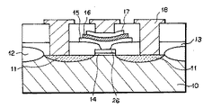
図10に示すような、強誘電体トランジスタを試作した。図10において、まず、p型シリコン(100)単結晶基板10を用い、フィールド酸化膜12を熱酸化法にて成膜、フォトリソグラフィー、エッチングによりトランジスタを作製するべき活性化領域を開口した。
【0052】
次に、ゲート絶縁膜としてSiON薄膜14、ゲート電極として多結晶シリコン膜26を形成、加工した後、このゲート電極部をマスクとして、イオン注入を行ない、ソース、ドレイン領域11を作製する。次に、レジストを剥離後、窒素雰囲気中約800℃にてアニールすることによってソース、ドレイン領域11を活性化した。さらに、層間絶縁膜として、酸化シリコン膜13を形成した。この結果、図11に示すような構造となる。
【0053】
次に、酸化シリコン膜13中のゲート電極部上部に、コンタクト穴を開口し、第一導電体膜15として、チタン、白金膜をスパッタリング法にて形成した。さらに、強誘電体薄膜16として(Sr(NbTa)2O7膜)を金属有機物を塗布焼成する方法によって形成する。膜厚は約300nmである。次に、第二導電体薄膜17として酸化イリジウムをスパッタリング法にて成膜した。膜厚は約150nmである。これを第二導電体薄膜17、強誘電体薄膜16、第一導電体膜26の順に、順次フォトリソグラフィー、ドライエッチングによって加工した。さらに、層間絶縁膜19としてプラズマCVD法にてシリコン酸化膜を形成し、その後、コンタクトホールをあけて、アルミニウム電極18をソース、ドレイン層11と第二導電体薄膜17上に形成、加工して完成となる。このサンプルの場合、実施形態1のサンプルAと同様に良好な特性を得ることができるが、コンタクト穴を明ける際、ゲート電極部との位置合わせ余裕を見込む必要があるため、サンプルAに比較して、ゲート長が0.75μmも長くなった。この結果、本実施形態の構造では、本発明の素子構造に比べかなり素子面積が大きくなってしまうことが明らかとなった。
【0054】
上記実施形態においては、強誘電体トランジスタ型不揮発性記憶素子の一素子について説明したが、このように形成された素子をマトリクス状に多数形成し、原理的にはDRAMと同程度以上の密度で集積する記憶装置とすることができる。また、この強誘電体トランジスタ型不揮発性記憶装置をICカードや携帯電話機等向けLSIに作り込み、ドライブ機構のない信頼性の高い安定した記憶素子として提供できる。
【0055】
また、ゲート電極をビット線、ソースをプレート線、ドレインをワード線として、各メモリセルを構成することにより、小さい駆動電圧で記憶機能のオン・オフを制御でき、信頼性の高い不揮発性記憶素子として確実に動作させることができる。
【0056】
【発明の効果】
本発明によれば、強誘電体端面のダメージ層を通じて流れるリーク電流、電荷注入を劇的に減らすことができ、結果としてメモリデバイスとしての記憶保持時間を伸ばすことができる。
【図面の簡単な説明】
【図1】本発明における素子構造の一例を示す断面図である。
【図2】本発明による強誘電体トランジスタの等価回路を示す図である。
【図3】本発明による実施形態1におけるサンプルAの構造を示す図である。
【図4】本発明による実施形態1におけるサンプルBの構造を示す図である。
【図5】本発明による実施形態1ににおけるサンプルAの製造過程で、ソース、ドレイン領域11をおおうように酸化膜を形成した後の構造を示す図である。
【図6】本発明による実施形態1におけるサンプルBの製造過程で、ソース、ドレイン領域11を活性化した後の構造を示す図である。
【図7】本発明による実施形態1におけるサンプルAを上から見た図である。
【図8】本発明による実施形態1におけるサンブルの電流一電圧特性の測定結果を示す図である。
【図9】本発明による実施形態1における試作サンプルの記憶保持特性の測定結果を示す図である。
【図10】本発明による実施形態2におけるサンブルの構造を示す図である。
【図11】本発明による実施形態2におけるサンブルの製造過程で、層間絶縁膜を形成した後の構造を示す図である。
【図12】従来の技術によるMFMIS構造を持つ、強誘電体トランジスタを示す図である。
【符号の説明】
1 半導体基板
2 ソース、ドレイン領域
3 フィールド酸化膜
4 ソース、ドレイン部をおおうシリコン酸化膜
5 酸素の拡散を阻止する絶縁性薄膜
6 第一導電体薄膜
7 強誘電体薄膜
8 第二導電体薄膜
9 アルミニウム配線
10 p型シリコン単結晶基板
11 ソース、ドレイン領域
12 フィールド酸化膜
13 ソース、ドレイン部をおおう熱酸化膜
14 SiON薄膜(絶縁性薄膜)
15 白金/チタン薄膜(第一導電体薄膜)
16 Sr(NbTa)2O7薄膜(強誘電体薄膜)
17 イリジウム薄膜(第二導電体薄膜)
18 アルミニウム配線
19 プラズマCVDシリコン酸化膜
20 シリコン多結晶基板
21 熱酸化シリコン酸化膜
22 多結晶シリコン電極
23 イリジウム、酸化イリジウム積層電極
24 強誘電体薄膜
25 イリジウム、酸化イリジウム積層電極
26 単結晶シリコン[0001]
BACKGROUND OF THE INVENTION
The present invention relates to a nonvolatile memory element, and more particularly to a ferroelectric transistor type nonvolatile memory element of a nonvolatile memory using a ferroelectric substance.
[0002]
[Prior art]
Recently, a FeRAM (
[0003]
Further, in this method, since the charge in the polarization inversion is extracted and detected as a current, the area of the capacitor is reduced and the current value is also reduced, which makes detection difficult. This is a fundamental problem that occurs because the cell structure of FeRAM does not follow the scaling law.
[0004]
In order to compare the amount of charge discharged from the ferroelectric capacitor, it is usually necessary to arrange a pair of reference cells in each cell. Therefore, two
[0005]
On the other hand, a ferroelectric transistor in which a ferroelectric is arranged at a gate portion of a field effect transistor (FET) can constitute a memory cell with a single transistor. In this device, the polarization of the ferroelectric induces the channel charge of the transistor to turn on and off between the source and drain, and even if the cell area is proportionally reduced, the rate of change in drain current does not change. . This means that the memory cell of the ferroelectric transistor follows the scaling rule (Journal of the Institute of Electronics, Information and Communication Engineers 77-9 p976, 1994), and there is no theoretical limit for miniaturization.
[0006]
The above is not only advantageous for reducing the cell area, but also the on / off of the FET is maintained by the polarization of the ferroelectric, so that information is not destroyed by the read operation, so-called nondestructive reading is performed. Is also possible.
[0007]
Further, the ferroelectric transistor in which the ferroelectric is arranged in the gate portion is roughly classified into two types. One of them is a ferroelectric transistor having an MFIS (Metal-Ferroelectric-Insulator-Semiconductor) structure, and the ferroelectric induces electric charges on the surface of the semiconductor substrate through the gate insulating film due to its polarization. One is a ferroelectric transistor having an MFMIS (Metal-Ferroelectric-Metal-Insulator-Semiconductor) structure, in which a metal electrode layer is sandwiched between a ferroelectric layer having an MFIS structure and an insulating layer.
[0008]
FIG. 2 shows the structure of these ferroelectric transistors in an equivalent circuit. From FIG. 2, when a voltage is applied between the
[0009]
In a conventional example of a ferroelectric transistor having an MFMIS structure (T. Nakamura et. Al. Dig. Tech. Pap. Of 1995 IEEE Int. Solid-State Circuits Conf. P. 68 (1995)), FIG. As shown in FIG. 4, a gate insulating
[0010]
For this reason, the gate portions of the silicon
[0011]
In this structure, since an alignment margin is required for the
[0012]
In addition, the ferroelectric transistor has a problem that the memory retention time becomes extremely short because the phenomenon of canceling the residual polarization of the ferroelectric occurs when the ferroelectric current leakage and charge injection occur. . Particularly, when charge injection occurs from the semiconductor substrate side, the channel of the FET disappears and information is lost in a short time. The gate insulating film formed on the semiconductor substrate is extremely thin, and charge injection and leakage current are likely to occur on the end surface processed by dry etching or the like.
[0013]
[Problems to be solved by the invention]
As described above, in the ferroelectric transistor having the MFMIS structure, the area of the ferroelectric capacitor needs to be smaller than the area of the gate insulating film. Further, there is a problem that the gate length cannot be reduced to the minimum processing size of the LSI manufacturing process. Further, the ferroelectric transistor has a problem that the memory holding time is shortened by the leakage current of the ferroelectric material and the charge injection into the ferroelectric material. It is considered that this leakage current and charge injection are likely to occur on the damaged gate insulating film and the end face of the ferroelectric.
[0014]
The present invention has been made to solve such an unsolved problem of the conventional technology, and enables the area of the ferroelectric capacitor to be smaller than the area of the gate insulating film, and the gate length to be set to LSI. Ferroelectric transistor-type non-volatile memory with excellent memory retention, which can be reduced to the minimum processing size of the manufacturing process, and prevents leakage current and charge injection at the damaged gate insulating film and ferroelectric end face. An element is provided.
[0015]
[Means and Actions for Solving the Problems]
A ferroelectric transistor type nonvolatile memory element according to the present invention includes an insulating thin film, a first conductive thin film, a ferroelectric thin film, and a second conductive thin film as a gate portion of a field effect transistor formed on a semiconductor substrate. Silicon oxide film covering source and drain regions in a ferroelectric transistor type nonvolatile memory element having a sequentially stacked structure Inner edge of And the insulating thin film Outer edge And the length of the first conductor thin film in the channel length direction is longer than that of the insulating thin film, and the end face of the first conductor thin film is disposed so as not to contact the end face of the insulating thin film. As the silicon oxide film, a thermal oxide film having a thickness larger than that of the insulating thin film is used. The silicon oxide film is formed by thermally oxidizing the semiconductor substrate using the insulating thin film as a mask. The inner edge of the oxide film is formed so as to be defined by the outer edge of the insulating thin film, and the first conductor thin film is formed along the upper surface of the silicon oxide film and the upper surface of the insulating thin film. It is characterized by that.
[0016]
In addition, as a gate part of a field effect transistor formed on a semiconductor substrate, a ferroelectric transistor type nonvolatile memory having a structure in which an insulating thin film, a first conductive thin film, a ferroelectric thin film, and a second conductive thin film are sequentially stacked. In a method for manufacturing an insulating memory element, a single crystal substrate mainly composed of silicon is used as a semiconductor substrate, the insulating thin film is formed and processed, a source region and a drain region are formed using the insulating thin film as a mask, and the insulating A silicon oxide film covering the source and drain regions by thermally oxidizing the surface of the semiconductor substrate using a conductive thin film as a mask Forming a first conductive thin film on the insulating thin film, applying and firing a metal organic ferroelectric thin film on the first conductive thin film, A second forming step of forming a second conductor thin film, and an outer edge of the first conductor thin film formed in the second forming step is located on the silicon oxide film It is characterized by that.
[0017]
Based on FIG. 1 which shows the outline | summary of this invention, the effect | action is demonstrated. A field effect transistor formed on a
[0018]
In the gate portion of the present invention, the insulating thin film 5 that prevents oxygen diffusion is used as the gate insulating film, and the first conductive
[0019]
Here, the writing, erasing and reading operations of the ferroelectric transistor type nonvolatile memory element of the present invention will be described with reference to FIG.
[0020]
In FIG. 1, an n-channel FET using a 5V drive p-type substrate will be described as an example. First, in the write operation, 5 V is applied to the second conductor
[0021]
In the ferroelectric transistor type memory device according to the present invention, the
[0022]
Further, by using the
[0023]
In the case of the present invention, after the insulating thin film is formed and processed, impurities are implanted to form the source and drain portions using the insulating thin film as a mask, and the portion not covered with the insulating thin film is thick. A
[0024]
The insulating thin film 5 in the present invention can be used not only as a mask for forming the
[0025]
As the first conductor
[0026]
Here, A and B represent metal elements. Further, by using the ferroelectric thin film 7 having a relative dielectric constant of 50 or less, a nonvolatile memory element having excellent memory retention characteristics can be obtained. In particular, Sr 2 Ta 2 O 7 Or Sr 2 (NbTa) 2 O 7 Or SrBi 2 Ta 2 O 9 As described above, it is more preferable to use a ferroelectric material having a lower relative dielectric constant.
[0027]
More preferably, the effective area of the ferroelectric capacitor is made smaller than the area of the channel region of the field effect transistor. The reason is that the structure of the gate portion is equivalent to a capacitor in which a ferroelectric thin film 7 and an insulating thin film 5 mainly composed of silicon nitride are connected in series as shown in FIG. When a voltage is applied to each thin film, the voltage is applied in inverse proportion to the capacity. Therefore, the relative dielectric constant of the ferroelectric substance is small, and the smaller the capacity, the higher the applied voltage and the saturation of the polarization, which is advantageous for memory retention. Because it becomes.
[0028]
Further, in the present invention, the
[0029]
Further, according to the present invention, after processing the insulating thin film 5 that prevents the diffusion of oxygen, the
[0030]
Here, we will compare with reports that have been studied. In a report made by Fujimori et al. In 1998 (Jpn. Appl. Phys. Vol.37 (1998) p.5207), Po1y-Si / SiO 2 / Pt / STN / IrO on top of gate electrode with Si / Si laminated structure 2 / Pt structure (STN is Sr 2 (TaNb) 2 O 7 It has a structure that connects ferroelectric capacitors. In this case, Po1y-Si / SiO 2 After the structure is formed and processed, the source portion and the drain portion are formed by ion implantation, an interlayer insulating film is formed, and contact holes for bonding to the ferroelectric capacitor are formed. Therefore, it is necessary to allow for an alignment margin for lithography, and POly-Si / SiO of the gate electrode portion. 2 The structure cannot be reduced to the minimum processing size, and there is a problem that the device area becomes large. On the other hand, in the present invention, this problem can be overcome as described above.
[0031]
The invention disclosed in Japanese Patent Laid-Open No. 5-135570 (inventor, Takashi Nakamura) is configured such that the gate electrode end face of the field effect transistor coincides with the ferroelectric capacitor electrode and the end face of the ferroelectric substance. However, in such a structure, a large amount of leakage current and charge injection occur through the end face of the damaged part, and the memory retention time becomes extremely short. On the other hand, the present invention can solve such problems by reducing leakage current and preventing charge injection.
[0032]
In the invention of Japanese Patent Laid-Open No. 5-121759 (inventor, Katsumi Kajishima), Po1y-Si / SiO 2 A gate electrode having a structure is embedded in an interlayer insulating film having a low dielectric constant, and an effect similar to that of the present invention can be obtained. However, in order to realize this structure, a sacrificial gate is used, and a source and a drain part are formed. After that, a low dielectric constant interlayer insulating film is formed, planarized using CMP (Chemical Mechanical Polishing), the sacrificial gate is removed, and a new Poly-Si / SiO 2 An extremely complicated manufacturing process is required in which a laminated structure is formed and planarization and embedding is performed again by CMP. In the present invention, the same effect can be obtained by a shorter manufacturing process as described above.
[0033]
Further, in the invention of Japanese Patent Application Laid-Open No. 11-145411 (inventor, Takashi Nakamura), SiO in the gate portion 2 On the gate area, the SiO 2 It is characterized by forming a ferroelectric capacitor area smaller than the area of, but since it is difficult to form the source part and the drain part by the self-alignment process, it is necessary to take a large alignment margin, There is a problem that the entire element becomes large. The publication does not require the use of a material that prevents oxygen diffusion in the gate insulating film, avoiding the problem of increasing the thickness of the gate insulating film during the ferroelectric heating and crystallization process. Can not. In the present invention, the thickness of the gate insulating film can be reduced, and such a problem can be solved.
[0034]
According to the present invention, a ferroelectric transistor with a small area can be manufactured because a margin for alignment can be secured even when the distance between the source and drain, which has been difficult with the conventional method, becomes the minimum processing dimension of the LSI manufacturing process. In addition, it is possible to separate the processing of the gate insulating film and the processing of the ferroelectric thin film, and to separate the end face of the ferroelectric or electrode that has been damaged by etching from the end face of the gate insulating film. A great effect can be obtained in reducing the leakage current in the dielectric thin film and the charge injection into the ferroelectric thin film, and the memory retention time can be greatly extended.
[0035]
Further, after using the silicon substrate, forming the insulating thin film 5 mainly composed of silicon nitride, and forming the
[0036]
As described above, according to the present invention, problems that are difficult to achieve with conventional ferroelectric transistors can be realized by an easy structure and manufacturing method.
[0037]
DETAILED DESCRIPTION OF THE INVENTION
Hereinafter, embodiments of the present invention will be described in detail with reference to the drawings.
[0038]
[Embodiment 1]
First, a ferroelectric transistor (sample A) as a nonvolatile memory element as shown in FIG. 3 and a ferroelectric transistor (sample B) as shown in FIG. 4 were produced as a comparative example. Both ferroelectric transistors use a p-type silicon (100)
[0039]
3 and 4, the field effect transistor formed on the
[0040]
The operation of the ferroelectric transistor nonvolatile memory element in FIG. 3 is the same as that in FIG. 1, but will be described again. Each operation of writing, erasing and reading of the ferroelectric transistor type nonvolatile memory element of the present invention will be described with reference to FIG.
[0041]
In FIG. 3, as an example of voltage application, a case of an n-channel FET using a 5V drive p-type substrate will be described. First, in the write operation, 5 V is applied to the second conductor
[0042]
Next, the reading operation will be described. The second conductor
[0043]
(Method for producing sample A)
In the case of sample A shown in FIG. 3, first, a SiON
[0044]
Next, a
[0045]
(Method for producing sample B)
Next, in the case of the sample B of the comparative example, as shown in FIG. 4, the SiON
[0046]
Next, phosphorus ions are ion-implanted into the sample to form source and drain
[0047]
Next, a silicon oxide film is formed as an
[0048]
For Samples A and B, a voltage was applied between the
[0049]
(Evaluation of sample A and sample B)
Next, memory retention characteristics are evaluated. For samples A and B, information is written by applying a voltage between the
[0050]
[Embodiment 2]
A ferroelectric transistor type nonvolatile memory element according to
[0051]
A ferroelectric transistor as shown in FIG. 10 was prototyped. In FIG. 10, first, a p-type silicon (100)
[0052]
Next, after forming and processing the SiON
[0053]
Next, a contact hole was opened in the upper part of the gate electrode portion in the
[0054]
In the above embodiment, one element of the ferroelectric transistor type nonvolatile memory element has been described. However, a large number of elements formed in this way are formed in a matrix, and in principle, at a density equal to or higher than that of a DRAM. The storage device can be integrated. Further, this ferroelectric transistor type nonvolatile memory device can be provided in an LSI for IC cards, mobile phones, etc., and provided as a highly reliable and stable memory element without a drive mechanism.
[0055]
In addition, by configuring each memory cell using a gate electrode as a bit line, a source as a plate line, and a drain as a word line, it is possible to control the on / off of the memory function with a small drive voltage, and a highly reliable nonvolatile memory element Can be operated reliably.
[0056]
【The invention's effect】
According to the present invention ,strength Leakage current and charge injection flowing through the damaged layer on the dielectric end face can be drastically reduced, and as a result, memory retention time as a memory device can be extended.
[Brief description of the drawings]
FIG. 1 is a cross-sectional view showing an example of an element structure in the present invention.
FIG. 2 is a diagram showing an equivalent circuit of a ferroelectric transistor according to the present invention.
FIG. 3 is a diagram showing a structure of a sample A in
FIG. 4 is a diagram showing a structure of a sample B in
5 is a view showing a structure after an oxide film is formed so as to cover a source /
6 is a view showing a structure after activation of a source /
7 is a top view of sample A in
FIG. 8 is a diagram showing measurement results of current-voltage characteristics of a sample in
FIG. 9 is a diagram showing measurement results of memory retention characteristics of a prototype sample according to
FIG. 10 is a diagram showing a structure of a sample in
FIG. 11 is a diagram showing a structure after an interlayer insulating film is formed in the manufacturing process of a sample in
FIG. 12 is a diagram showing a ferroelectric transistor having a MFMIS structure according to the prior art.
[Explanation of symbols]
1 Semiconductor substrate
2 Source and drain regions
3 Field oxide film
4 Silicon oxide film covering source and drain
5 Insulating thin film that prevents oxygen diffusion
6 First conductor thin film
7 Ferroelectric thin film
8 Second conductor thin film
9 Aluminum wiring
10 p-type silicon single crystal substrate
11 Source and drain regions
12 Field oxide film
13 Thermal oxide film covering source and drain
14 SiON thin film (insulating thin film)
15 Platinum / titanium thin film (first conductor thin film)
16 Sr (NbTa) 2 O 7 Thin film (ferroelectric thin film)
17 Iridium thin film (second conductor thin film)
18 Aluminum wiring
19 Plasma CVD silicon oxide film
20 Silicon polycrystalline substrate
21 Thermally oxidized silicon oxide film
22 Polycrystalline silicon electrode
23 Iridium and iridium oxide laminated electrodes
24 Ferroelectric thin film
25 Iridium and iridium oxide laminated electrodes
26 Single crystal silicon
Claims (10)
ソース領域およびドレイン領域を覆うシリコン酸化膜の内縁と前記絶縁性薄膜の外縁とが接合し、かつ前記第一導電体薄膜のチャネル長方向の長さが前記絶縁性薄膜より長く、前記第一導電体薄膜の端面が前記絶縁性薄膜の端面と接触しないように配置され、
前記シリコン酸化膜として、前記絶縁性薄膜より膜厚が厚い熱酸化膜が用いられ、
前記シリコン酸化膜は、前記絶縁性薄膜をマスクとして用いて前記半導体基板を熱酸化させることにより、前記シリコン酸化膜の内縁が前記絶縁性薄膜の外縁により規定されるように形成され、
前記第一導電体薄膜が前記シリコン酸化膜の上面及び前記絶縁性薄膜の上面に沿うように形成されている
ことを特徴とする強誘電体トランジスタ型不揮発性記憶素子。A ferroelectric transistor type nonvolatile memory having a structure in which an insulating thin film, a first conductive thin film, a ferroelectric thin film, and a second conductive thin film are sequentially stacked as a gate portion of a field effect transistor formed on a semiconductor substrate. In the element
The inner edge of the silicon oxide film covering the source region and the drain region is joined to the outer edge of the insulating thin film, and the length in the channel length direction of the first conductive thin film is longer than that of the insulating thin film, Arranged so that the end face of the body thin film does not contact the end face of the insulating thin film ,
As the silicon oxide film, a thermal oxide film that is thicker than the insulating thin film is used,
The silicon oxide film is formed such that an inner edge of the silicon oxide film is defined by an outer edge of the insulating thin film by thermally oxidizing the semiconductor substrate using the insulating thin film as a mask.
The ferroelectric transistor type nonvolatile memory element, wherein the first conductive thin film is formed along the upper surface of the silicon oxide film and the upper surface of the insulating thin film .
半導体基板としてシリコンを主体とする単結晶基板を用い、前記絶縁性薄膜を形成、加工し、前記絶縁性薄膜をマスクとしてソース領域およびドレイン領域を形成し、前記絶縁性薄膜をマスクとして前記半導体基板表面を熱酸化することによって、前記ソース領域およびドレイン領域を覆うシリコン酸化膜を形成する第1形成工程と、
前記第1形成工程後に、前記絶縁性薄膜上に第一導電体薄膜を形成し、前記第一導電体薄膜上に金属有機物の強誘電体薄膜を塗布焼成し、次に、第二導電体薄膜を形成する第2形成工程と
を有し、
前記第2形成工程において形成される前記第一導電体薄膜の外縁が前記シリコン酸化膜上に位置する
ことを特徴とする強誘電体トランジスタ型不揮発性記憶素子の製造方法。A ferroelectric transistor type nonvolatile memory having a structure in which an insulating thin film, a first conductive thin film, a ferroelectric thin film, and a second conductive thin film are sequentially stacked as a gate portion of a field effect transistor formed on a semiconductor substrate. In the manufacturing method of the element,
Using a single crystal substrate mainly made of silicon as a semiconductor substrate, forming and processing the insulating thin film, forming a source region and a drain region using the insulating thin film as a mask, and using the insulating thin film as a mask, the semiconductor substrate A first forming step of forming a silicon oxide film covering the source region and the drain region by thermally oxidizing the surface ;
After the first forming step, a first conductor thin film is formed on the insulating thin film, a metal organic ferroelectric thin film is applied and baked on the first conductor thin film, and then a second conductor thin film is formed. A second forming step of forming
Have
The manufacturing method of a ferroelectric transistor type nonvolatile memory element, wherein an outer edge of the first conductive thin film formed in the second forming step is located on the silicon oxide film .
Priority Applications (1)
| Application Number | Priority Date | Filing Date | Title |
|---|---|---|---|
| JP29708999A JP4459335B2 (en) | 1999-10-19 | 1999-10-19 | Ferroelectric transistor type nonvolatile memory element and manufacturing method thereof |
Applications Claiming Priority (1)
| Application Number | Priority Date | Filing Date | Title |
|---|---|---|---|
| JP29708999A JP4459335B2 (en) | 1999-10-19 | 1999-10-19 | Ferroelectric transistor type nonvolatile memory element and manufacturing method thereof |
Publications (3)
| Publication Number | Publication Date |
|---|---|
| JP2001118941A JP2001118941A (en) | 2001-04-27 |
| JP2001118941A5 JP2001118941A5 (en) | 2006-11-30 |
| JP4459335B2 true JP4459335B2 (en) | 2010-04-28 |
Family
ID=17842071
Family Applications (1)
| Application Number | Title | Priority Date | Filing Date |
|---|---|---|---|
| JP29708999A Expired - Fee Related JP4459335B2 (en) | 1999-10-19 | 1999-10-19 | Ferroelectric transistor type nonvolatile memory element and manufacturing method thereof |
Country Status (1)
| Country | Link |
|---|---|
| JP (1) | JP4459335B2 (en) |
-
1999
- 1999-10-19 JP JP29708999A patent/JP4459335B2/en not_active Expired - Fee Related
Also Published As
| Publication number | Publication date |
|---|---|
| JP2001118941A (en) | 2001-04-27 |
Similar Documents
| Publication | Publication Date | Title |
|---|---|---|
| JP4775849B2 (en) | SEMICONDUCTOR ELEMENT, SEMICONDUCTOR MEMORY DEVICE USING SAME, DATA WRITE METHOD, DATA READ METHOD, AND MANUFACTURING METHOD THEREOF | |
| US5940705A (en) | Methods of forming floating-gate FFRAM devices | |
| KR100406536B1 (en) | FeRAM having aluminum oxide layer as oxygen diffusion barrier and method for forming the same | |
| US20070158731A1 (en) | Memory Devices Employing Ferroelectric Layer as Information Storage Elements and Methods of Fabricating the Same | |
| WO2001024265A1 (en) | Nonvolatile memory | |
| US6885048B2 (en) | Transistor-type ferroelectric nonvolatile memory element | |
| JPH0437170A (en) | Manufacture of semiconductor device | |
| JP3977079B2 (en) | Ferroelectric transistor and its use in memory cell structure | |
| JPH09116036A (en) | Non-volatile storage cell transistor | |
| US6944044B2 (en) | Method for reading out or in a status from or to a ferroelectrical transistor of a memory cell and memory matrix | |
| US6046927A (en) | Nonvolatile semiconductor memory device, a method of fabricating the same, and read, erase write methods of the same | |
| WO2018186035A1 (en) | Semiconductor memory element, semiconductor memory device, semiconductor system and control method | |
| JP4459335B2 (en) | Ferroelectric transistor type nonvolatile memory element and manufacturing method thereof | |
| JP3160325B2 (en) | Semiconductor storage element | |
| JP3849105B2 (en) | Manufacturing method of ferroelectric memory | |
| US7511325B2 (en) | Ferroelectric capacitor | |
| JP3093011B2 (en) | FIELD-EFFECT TRANSISTOR AND ITS MANUFACTURING METHOD, AND NONVOLATILE STORAGE ELEMENT AND NONVOLATILE STORAGE DEVICE USING THE TRANSISTOR | |
| JP4827316B2 (en) | Method for driving ferroelectric transistor type nonvolatile memory element | |
| JP3210292B2 (en) | Ferroelectric memory device and driving method thereof | |
| JP2002329843A (en) | Ferroelectric transistor type nonvolatile storage element and its manufacturing method | |
| JP3095271B2 (en) | Thin-film field-effect transistor, method of manufacturing the same, and nonvolatile storage element and nonvolatile storage device using the transistor | |
| JPH09321237A (en) | Non-volatile semiconductor storage device having ferroelectric film, capacitor having ferroelectric film and its manufacture | |
| JPH08191134A (en) | Semiconductor memory cell and manufacture thereof | |
| JPH1027856A (en) | Nonvolatile semiconductor memory and manufacture thereof | |
| KR20050038298A (en) | Transistor structure for based on ferroelectric a semiconductor |
Legal Events
| Date | Code | Title | Description |
|---|---|---|---|
| A521 | Request for written amendment filed |
Free format text: JAPANESE INTERMEDIATE CODE: A523 Effective date: 20061016 |
|
| A621 | Written request for application examination |
Free format text: JAPANESE INTERMEDIATE CODE: A621 Effective date: 20061016 |
|
| RD04 | Notification of resignation of power of attorney |
Free format text: JAPANESE INTERMEDIATE CODE: A7424 Effective date: 20090220 |
|
| RD03 | Notification of appointment of power of attorney |
Free format text: JAPANESE INTERMEDIATE CODE: A7423 Effective date: 20090302 |
|
| RD03 | Notification of appointment of power of attorney |
Free format text: JAPANESE INTERMEDIATE CODE: A7423 Effective date: 20090313 |
|
| A521 | Request for written amendment filed |
Free format text: JAPANESE INTERMEDIATE CODE: A821 Effective date: 20090313 |
|
| A977 | Report on retrieval |
Free format text: JAPANESE INTERMEDIATE CODE: A971007 Effective date: 20090624 |
|
| A131 | Notification of reasons for refusal |
Free format text: JAPANESE INTERMEDIATE CODE: A131 Effective date: 20090629 |
|
| A521 | Request for written amendment filed |
Free format text: JAPANESE INTERMEDIATE CODE: A523 Effective date: 20090828 |
|
| A131 | Notification of reasons for refusal |
Free format text: JAPANESE INTERMEDIATE CODE: A131 Effective date: 20091009 |
|
| TRDD | Decision of grant or rejection written | ||
| A01 | Written decision to grant a patent or to grant a registration (utility model) |
Free format text: JAPANESE INTERMEDIATE CODE: A01 Effective date: 20100115 |
|
| A01 | Written decision to grant a patent or to grant a registration (utility model) |
Free format text: JAPANESE INTERMEDIATE CODE: A01 |
|
| A61 | First payment of annual fees (during grant procedure) |
Free format text: JAPANESE INTERMEDIATE CODE: A61 Effective date: 20100210 |
|
| R150 | Certificate of patent or registration of utility model |
Free format text: JAPANESE INTERMEDIATE CODE: R150 |
|
| FPAY | Renewal fee payment (event date is renewal date of database) |
Free format text: PAYMENT UNTIL: 20130219 Year of fee payment: 3 |
|
| FPAY | Renewal fee payment (event date is renewal date of database) |
Free format text: PAYMENT UNTIL: 20140219 Year of fee payment: 4 |
|
| R250 | Receipt of annual fees |
Free format text: JAPANESE INTERMEDIATE CODE: R250 |
|
| R250 | Receipt of annual fees |
Free format text: JAPANESE INTERMEDIATE CODE: R250 |
|
| R250 | Receipt of annual fees |
Free format text: JAPANESE INTERMEDIATE CODE: R250 |
|
| R250 | Receipt of annual fees |
Free format text: JAPANESE INTERMEDIATE CODE: R250 |
|
| LAPS | Cancellation because of no payment of annual fees |