JP4454793B2 - IMAGING DEVICE AND CONTROL METHOD OF IMAGING DEVICE - Google Patents
IMAGING DEVICE AND CONTROL METHOD OF IMAGING DEVICE Download PDFInfo
- Publication number
- JP4454793B2 JP4454793B2 JP2000155316A JP2000155316A JP4454793B2 JP 4454793 B2 JP4454793 B2 JP 4454793B2 JP 2000155316 A JP2000155316 A JP 2000155316A JP 2000155316 A JP2000155316 A JP 2000155316A JP 4454793 B2 JP4454793 B2 JP 4454793B2
- Authority
- JP
- Japan
- Prior art keywords
- exposure
- timing
- signal
- light emission
- time
- Prior art date
- Legal status (The legal status is an assumption and is not a legal conclusion. Google has not performed a legal analysis and makes no representation as to the accuracy of the status listed.)
- Expired - Fee Related
Links
Images


Description
【0001】
【発明の属する技術分野】
本発明は、静止画像や動画像を撮像する撮像装置と、該撮像装置の制御方法に関する。
【0002】
【従来の技術】
従来より、撮像素子を利用して静止画像や動画像を撮像する電子カメラ等の撮像装置では、被写界画像を撮像素子に結像させ、撮像素子から得られる画像データ(被写界輝度データ)を積分し、斯かる積分データに基づいて露出制御や調光制御等を行うTTL(スルー・ザ・レンズ)方式の露光技術が利用されている。該TTL方式で露光制御を行う場合、閃光を伴う撮影の場合は、まず外光のみの画像データを積分測光して第1の積分データを取得した後、予備発光を行い、外光とストロボ光とが混在した状態での画像データを積分測光して第2の積分データを取得し、第1の積分データと第2の積分データとに基づいて本露光時の発光時間(発光量)を決定している。
【0003】
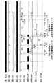
図4はTTL方式で露光制御を行う場合の従来の制御手順を示すタイムチャートである。
【0004】
この種の撮像装置では、図4(i)に示すように、撮影用の電源オン時には撮像素子を駆動させるためのクロックCLKが常時出力しており、該クロックCLKに基づいて図4(ii)に示すような水平同期信号HD、図4(iii)に示すような垂直同期信号VD、図4(vi)に示すような撮像素子に蓄積された電荷を読み出す信号SG及び、図4(vii)撮像素子に蓄積された不要な電荷を除去する不要電荷除去信号SUBを発生させている。
【0005】
また、該撮像装置は、撮影準備駆動モードや撮影駆動モードに代表される複数の撮像駆動モードを有し、夫々の撮像駆動モードに最適な前記タイミング信号群を形成し、駆動モードの切換は、垂直同期期間を分解能として行うのが一般的である。
【0006】
撮像素子における露光とは、SUB信号出力停止から次の垂直転送期間のSG信号出力までに電荷を蓄積することを意味し、図4(i)中の垂直転送期間AからBにかけて行われる露光について言えば、図4(vi)(vii)中のiタイミングからh´タイミングまでが該当する。勿論、画像データを量子化する際に得られる画像データがダイナミックレンジに対して適切であるようにSUB信号の出力数を調節しているのは言うまでもない(公知の電子シャッタ機能)。また、露光された画像データはSG信号の出力に応じて順次読み出され、読み出された画像データを量子化した後、画像データの輝度成分を信号処理部において積分して被写界輝度を測光演算する。
【0007】
すなわち、撮像装置が撮影準備駆動モードに設定され、時間t1で垂直同期信号VDがアクティブになると、該垂直同期信号VDの立下りエッジをトリガとして時間t2で撮像素子の読出信号SGが生成されると共に(図4(vi))、次の露光のために不要電荷除去信号SUBを所定数出力させて撮像素子に蓄積される露光時間を制御する(図4(vii))。さらに並行して、SG信号以後撮像素子から順次読み出される画像データの輝度成分を信号処理部で積分し、外光のみによる第1の積分データを取得する(図4(viii)中、aで示す)。
【0008】
そして、閃光を伴う場合は、図4(x)に示すように、時間t4で閃光開始及び停止信号STSPを発生させて予備発光を行う。すなわち、今回の露光期間(図4(ix)中、bで示す)内に予備発光を行う。
【0009】
そして、次の垂直転送期間Cで読み出される予備発光を含む被写界輝度データを積分し、外光と閃光が混在した第2の積分データを取得する(図4(viii)中、cで示す)。この後第1及び、第2の積分データに基づいて主被写体の反射率を演算して、本露光時の発光時間(発光量)を求める。
【0010】
次いで、撮像素子を撮影駆動モードに切換えるべく、VD信号のアクティブタイミングや、SG信号の発生タイミング、垂直同期期間が変動したことによるSUB信号の出力数を設定変更する。しかしながら先にも述べたように、SG信号やSUB信号はVDのアクティブタイミング即ちVD信号の立下りを基準にして出力タイミングや出力数が更新されるため、第2の積分データを取得してから、測光演算や発光時間演算等が完了した時にVD信号のアクティブタイミングが過ぎてしまうと、垂直転送期間の変更は出来ても、SG信号やSUB信号の変更は更新されない。したがって、図に示すように、次にVDがアクティブになるまで無駄に時間(図4(v)中の垂直転送期間D)を浪費する可能性が高かった。
【0011】
更に、SG信号やSUG信号の設定変更が更新される次の垂直転送期間EでSUB信号出力が停止と共に電荷の蓄積即ち、本露光を開始する。そして、本露光開始後の時間t7で閃光開始及び停止信号STSPを発生させ、前記発光時間の間に本発光を行い、露光完了となるt8タイミングで本露光を終了すべく、シャッタを閉じて被写体の撮像素子への供給を遮断する。
【0012】
このように不要電荷除去信号SUBの出力停止タイミング(時間t6)からシャッタの駆動開始タイミング(時間t8)までが本露光の露光時間eとなり、該露光時間e内で本発光を行っている。但し一般的に、シャッタには制御タイミングから実際の遮蔽開始動作に至るまでに機械的な遅延時間があり、上記シャッタの駆動開始タイミング(時間t8)は、シャッタ固有の遅延時間を考慮して決定している。
【0013】
そして、シャッタが完全に閉じる時間経過後(時間t9)、最初に現れる垂直同期信号VDのアクティブタイミング以降の垂直転送期間F内の時間t11で読出信号SGを発生させて第1フィールドから画像データデータを読み出し、信号処理を施した後メモリ部へ転送を行い、引き続き、次の垂直転送期間(不図示)で第2フィールドの画像データを読み出し、第1フィールドと同様にしてメモリ部へ転送を行っている。
【0014】
【発明が解決しようとする課題】
ところで、TTL方式で調光制御を行う場合は、予備発光と本発光との発光間隔は、予備発光の閃光によって瞼を閉じてしまうまでの時間よりも短いことが重要であり、特に、暗中における人物撮影時には必須条件と考えられている。しかしながら、撮像素子を用いた撮像装置では、原理的に撮像素子に露光させた被写界画像をリアルタイムに積分することができない。つまり、露光の完了が撮像素子に蓄積された電荷の読み出しであるため、露光したフィールドの画像データを積分できるのは、読み出した後に相当する次のフィールドに他ならない。このように、単一露光フィールドと該露光フィールドで得られた画像データの積分とを並列処理できないため、発光間隔(図4中、dで示す)を短くするのが容易でないという問題点があった。
【0015】
すなわち、図4に示すように、予備発光を伴う垂直転送期間Bと垂直転送期間Cに跨った露光フィールドと、本発光を行う垂直転送期間Eの間には、2つの垂直転送期間が存在してしまう。一つ目は、予備発光が行われた画像データを積分するために必要な垂直転送期間であり、省くことはできない。二つ目は、先に述べた通り、撮像素子の駆動方式を変更するためのトリガとなる垂直同期信号VDのアクティブ期間の発生間隔を正規の垂直転送レートで行っているために、 SG信号やSUB信号の出力タイミングや出力数が更新されるまで無駄に消費する垂直転送期間である。この時間は、撮像素子に蓄積された画像データを垂直方向に転送するレートに比例して長短し、レリーズタイムラグ等に影響を及ぼす要因の一つである。
【0016】
また、予備発光や本発光の閃光開始、更には停止信号STSPの発生タイミングに応じて発光間隔dが変動する。例えば、図4(x)の実線で示すように、予備発光の発光タイミングを露光期間bの開始直後に設定し且つ、本発光の発光タイミングを露光期間eの開始直後に設定した場合、予備発行の露光期間bの長さに応じて本発光までの発光間隔dが変動し、また、本露光を開始するための不要電荷除去信号SUBの出力停止タイミング(時間t6)を本露光の露光時間eに応じて変動させた場合は、発光間隔dは被写界輝度によって変動する。
【0017】
さらに、予備発光、及び本発光の発光タイミングを図4(x)の破線に示すように、露光期間b、eの終了直前に行った場合は、予備発酵の露光機関bの影響は受けないが、本露光の露光期間eによって発光間隔d、及びシャッタを完全に閉じてから次の垂直同期信号VDが発生する時間t10までの時間fが変動する。斯かる期間fが長くなると、読出信号SGの発生も遅延するため、画像データの読み出し開始が遅くなるという問題があった。しかも、シャッタの遮蔽制御開始時間t8からシャッタが実際に遮蔽状態になるまでの時間t9は、シャッタ個別に変動する。
【0018】
斯かる期間fが長く、そして安定しない撮像装置においては、シャッタによって撮像素子への被写界像の供給を遮断してから、実際に露光された画像データが読み出されるまでの期間gは露光期間eに応じて変動し、該期間gが長くなると、撮像素子が実装されている基盤への蓄積された電化の流出度合いが変動し、一定した品質の画像データが得られなく虞なるがある。特に、複数の垂直転送期間に跨って露光を行うような長秒時露光で、シャッタが遮光状態になる時間t9がSG信号の出力タイミングt11直後である場合が最も電荷の流出が激しい。
【0019】
さらに、撮像素子の色フィルタ配列によっては第1フィールドと第2フィールドにおける色による感度若しくは、飽和レベルが異なり、いずれのフィールドから先行して読み出すかを任意に設定するのは困難である。
【0020】
本発明はこのような事情に鑑みてなされたものであって、閃光を伴う撮影の場合に、予備発光と本発光との発光間隔を大幅に短縮し、これにより品質の良好な画像データを迅速にえることができる撮像装置と該撮像装置の制御方法を提供することを目的とする。
【0021】
【課題を解決するための手段】
上記目的を達成するために本発明に係る撮像装置は、光学情報を電気情報に変換する撮像手段の所定の露光期間に蓄積された当該電気信号を転送するタイミングである垂直同期信号の発生を制御するタイミング発生手段と、撮像された画像の輝度を導出する測光手段と、前記測光手段の導出結果に基づいて前記撮像手段における露出条件を制御する露出制御手段と、被写界に閃光を照射する閃光発光タイミング信号を生成する閃光タイミング手段と、閃光を伴う本露光前に予備発光を行って本露光の際の閃光発光量を決定する調光制御手段とを有し、前記タイミング発生手段は、前記垂直同期信号を第1の発生間隔と当該第1の発生間隔よりも短い間隔の第2の発生間隔で発生可能であって、前記閃光タイミング手段は、前記第1の発生間隔で発生する前記垂直同期信号に応じた前記予備発光を伴う露光期間の終了位置を基準に前記予備発光を行い、当該予備発光を伴った露光により蓄積された電気信号を転送した後に前記第2の発生間隔で前記垂直同期信号を発生させ、当該発生された前記垂直同期信号の後の本露光の露光期間の開始位置を基準に前記本露光発光を行うことを特徴としている。
【0027】
尚、本発明のその他の特徴は下記の発明の実施の形態の記載により明らかとなろう。
【0028】
【発明の実施の形態】
次に、本発明の実施の形態を図面に基づいて詳説する。
【0029】
図1は、本発明に係る撮像装置の一実施の形態を示すブロック構成図であって、該撮像装置は、被写体としての光学像を電気信号に変換し、量子化された画像データを供給する撮像ブロック1と、該撮像ブロック1から出力される画像データに所定の信号処理を施す信号処理ブロック2と、装置本体に内蔵若しくは接続された閃光装置3とから構成されている。
【0030】
撮像ブロック1は、被写界像が透過するレンズ群4と、該レンズ群4を透過した被写界像(光学像)が結像し該光学像を電気信号に変換する撮像素子5と、光学像を前記撮像素子5上に合焦させるための合焦系レンズ6と、絞り7と、被写界像の撮像素子5への入射を遮断するシャッタ8と、撮像素子5により電気信号に変換されたアナログ画像信号をデジタル画像信号に変換するA/D変換器9と、前記撮像素子5を駆動させるための各種タイミング信号を発生するタイミング発生部10と、絞り7の切換やシャッタ8の開閉制御を指令する露光制御部11と、装置本体に内蔵若しくは、接続される閃光装置の発光制御を行う閃光制御部12とを有している。
【0031】
タイミング発生部10は、撮像素子を駆動する基準クロック(例えば、18MHz)単位で計数する複数の同期カウンタを有し、該同期カウンタの計数値基づいて水平同期信号HD及び、垂直同期信号VDを発生させ、さらにカウンタ値適宜変更することにより垂直同期信号VDのアクティブ期間の発生間隔、すなわち垂直転送期間の変更を可能としている。
【0032】
また、垂直同期信号VDのアクティブタイミング(立下りエッジ)によってリセットされ、該垂直同期信号VDのアクティブタイミングから基準クロックCLK単位で計数するカウンタを内蔵し、撮像駆動モード(撮像素子に依存)に応じて、撮像素子5に蓄積された電荷を読み出す読出信号SG及び、不要電荷除去信号SUB等を発生させ、撮像素子5を駆動させるための各種信号の発生タイミング等を制御する。
【0033】
閃光制御部12及び露光制御部11には、例えば10MHzを基準クロックとして計数する閃光パルス生成用カウンタ及び、シャッタパルス生成用カウンタが内蔵されており、閃光制御部12及び露光制御部11は1μsec単位でパルスを形成する。上記両カウンタは計数を停止し且つカウント値をゼロにリセットする設定と、カウント動作開始から信号を反転させるカウント値の設定と、反転された信号を元の状態に戻すカウント値の設定が出来るように構成される。信号処理ブロック2のシステム制御部15は、上記パルスの生成に必要な設定を行ない、予備発光、本発光、及び本露光時のシャッタ遮蔽制御の開始タイミング、更にはパルス幅を調節する。
【0034】
また、信号処理ブロック2は、撮像ブロックから出力された画像データに対し所定の信号処理を行う信号処理部13と、該信号処理部で信号処理された画像データ等を記憶するメモリ部14と、信号処理部13及び、撮像ブロックに接続されて装置全体を制御するシステム制御部15とを有している。
【0035】
尚、信号処理部13は、撮像ブロック1から出力された画像データに対し、所定領域で積分する積分回路を備える他、画像データのデータ変換や有効領域の切り出し等の信号処理された画像データをメモリ部14の所定のアドレスに転送するメモリ制御回路を備えている。
【0036】
また、閃光装置3は、閃光制御部12から出力される閃光開始及び停止信号STSPがHiの期間に発光するように構成されている。
【0037】
図2は本撮像装置の制御手順を示すフローチャートである。
【0038】
まず、ステップS1で撮像電源を投入し、続くステップS2では撮像素子5を撮影準備駆動モードに設定する。次いで、ステップS3で被写界画像データを複数に分割し、分割された領域の大きさ、即ち積分領域を信号処理部13に設定する。次いで、ステップS4で露光制御部11の制御下、シャッタ8を開状態として絞り7を調整し露出制御を行う。そして続くステップS5では積分測光を行い、撮像素子5から連続的に得られる被写界画像データを積分し、第1の積分データを取得する。
【0039】
次に、ステップS6ではステップS5で得られた第1の積分データに基づいて測光演算し、ステップS7で適正露出が得られたか否かを判断する。そして、適正露出が得られなかった場合はステップS4にもどって適正な露出が得られるまで上記処理を繰り返す。そして、適正な露出が得られると、ステップS7の答えは肯定(Yes)となってステップS8に進み、閃光を伴う撮影か否かを判断し、閃光を伴わない撮影の場合はステップS12に進む一方、閃光を伴う撮影の場合にはステップS9で予備発光を行い、続くステップS10では予備発光で得られた被写界輝度データを積分測光して第2の積分データを取得し、次いでステップS11ではステップS5で得られた外光のみの第1の積分データとステップS10で得られた外光及び閃光が混在した第2の積分データとに基づいて調光演算を行い、本露光時の発光時間及び露光時間(発光量)を算出する。
【0040】
そして、ステップS12では撮像素子5を撮影駆動モードに切換え、タイミング発生部10のカウンタ値及び、カウンタ動作を制御して垂直同期信号VDの発生間隔を短縮させ、正規の垂直転送期間(図3中、V0、V1若しくは、Vに示す)よりも発生間隔の短い第1の短縮垂直転送期間V3を生成し、続くステップS13では閃光に伴う撮影か否かを判断し、閃光を伴わない撮影の場合はステップS15に進む一方、閃光を伴う撮影の場合はステップS14で本発光を行う。
【0041】
そして、続くステップS15では露光時間に応じてシャッタ8を閉じ始め、その後、前記正規の垂直転送期間よりも短い第2の短縮垂直転送期間V2を生成し、ステップS16で画像データを読み出してメモリ部14に転送し、処理を終了する。上記画像データの読み出しは、上記第2の短縮垂直転送期間以後の第1の垂直転送期間に、第1フィールド、又は第2フィールドから読み出され、第1の垂直転送期間直後の第2の垂直転送期間に、第1の垂直転送期間で読み出したフィールドでない第2フィールド或いは、第1フィールドを読み出し、夫々を所定のメモリのアドレスに転送を行う。
【0042】
図3は閃光を伴う撮影の場合の各制御タイミングを示すタイムチャートである。
【0043】
上述したようにタイミング発生部10は、撮像電源オン時は基準クロック単位(例えば18MHz)でクロック信号CLKを常時出力すると共に(図3(i))、複数のカウンタを有し、斯かるカウンタの動作及び、各タイミング信号の挙動を決定するカウント値を制御してカウント値を計数することにより、水平同期信号HD及び、垂直同期信号VDが発生する(図3(ii)、(iii))。
【0044】
例えば水平同期信号は、アクティブ期間を前記基準クロックの50CLK、非アクティブ期間を1800CLKとし、Hカウンタが1800CLKを計数した時点でカウンタをゼロにリセットするように構成する。勿論、上記それぞれの計数値は信号処理ブロック2のシステム制御部15によってプログラムできるように構成され、設計する撮像装置(撮像素子に依存)に応じて変更可能とする。また垂直同期信号は、上記水平同期信号を基準として、アクティブ期間を7H、非アクティブ期間を撮像駆動モードに応じて、300H、600H(撮像素子に依存)とし、Vカウンタが前記設定値を計数した時点でゼロにリセットするように構成し(図3中(ii)、(iii)参照)、プログラマブルであるのは同様である。
そして、撮像素子5が撮影準備駆動モードに設定され、時間T1で垂直同期信号VDが発生すると(図3(iii)、(v))、該垂直同期信号のアクティブ期間(立下りエッジ)をトリガとして時間T2で読出信号SGが発生し(図3(vi))、さらに不要電荷除去信号SUBの出力を開始して、露光時間に応じて撮像素子5に蓄積されている不要な電荷を除去する(図3(vii))。
【0045】
先に述べた通り、読出信号SG、及び不要電荷除去信号SUBの生成は、垂直同期信号VDのアクティブタイミング(立下りエッジ)によってリセットされ且つ、該垂直同期信号VDのアクティブタイミングから基準クロックCLK単位で計数するカウンタを用いて行われ、撮像駆動モードに応じて、撮像素子5を駆動させるための各種信号の発生タイミング等を制御する。勿論、上記夫々の信号を発生させるタイミングを決定するカウンタの計数値は、信号処理ブロック2のシステム制御部15によってプログラムできるように構成されるのは言うまでもない。
【0046】
そして、時間T2以前の垂直転送期間に露光された画像データをT2タイミングで発生する読出信号SGで逐次読み出すと共に、信号処理部13に設定された積分領域(図3(viii)中、符号Aで示す)内の画像データの輝度成分を積分し、第1の積分データを取得する。そしてその後、時間T4で閃光装置3を駆動させて予備発光を行う。
【0047】
この予備発行の発光タイミングは、閃光制御部12に内蔵された上記閃光パルス生成用カウンタの動作設定により制御される。具体的には、まず時間T1以前に閃光制御部12の閃光パルス生成用カウンタはゼロにリセットされた状態で停止させておく。次に、予備発光の露光期間Bが終了し、読出信号SGが出力される時間T5までの間に、予め発光時間が決定している予備発光が完了するように、閃光パルス生成用カウンタのカウント値を逆算し、カウント動作開始から信号を反転させるカウント値の設定と、反転された信号を元の状態に戻すカウント値の設定を行う。そして、時間T1でカウント動作を開始させ、上記閃光パルス生成用カウンタが設定された夫々のカウント値に到達した時点で、閃光開始及び停止信号STSPのパルスが生成され予備発光が時間T4で行われる。尚、上記発光タイミングの逆算は、垂直同期信号VDのアクティブタイミング(時間T1)からのカウント値として求められる。また、予備発光完了後(時間T5以降)、上記閃光パルス生成用のカウンタを停止し、カウントの計数値をゼロにリセットする。
【0048】
そして、時間T5以前の垂直転送期間に露光された閃光を伴う画像データをT5タイミングで発生する読出信号SGで逐次読み出すと共に、信号処理部13に設定された積分領域(図3(viii)中、符号Cで示す)内の画像データの輝度成分を積分し、第2の積分データを取得する。次いで、外光のみの前記第1の積分データと、外光と閃光の混在した第2の積分データに基づいた測光演算を行って、主被写体の反射率を演算し、本露光時の発光時間と露光時間(発光量)を算出する。続いて、求められた発光時間と、露光時間に基づいて、前記閃光パルス生成用カウンタと、前記シャッタパルス生成用カウンタの設定を、垂直同期信号のアクティブタイミング(立下りエッジ)からのカウンタ計数値で行う。ここでは、予め撮像素子5に依存した撮影駆動モードにおける垂直転送期間の時間と、読み出しフィールドの属性(第1フィールド若しくは、第2フィールド)、読出信号SGの出力タイミング及び、不要電荷除去信号SUBの出力本数に基づいて、カウンタ値を求める。尚、本露光時の不要電荷除去信号SUBの出力本数は、予備発光から本発光までの時間を最小にするため、最小本数に固定する。最小本数は撮像素子5に依存して変化するが、必要最小限であることに変わりはない。また、前記閃光パルス生成用カウンタにおける発光開始タイミングを決定するカウント計数値は、上記本露光時の不要電荷除去信号SUBの出力が停止した以降の近傍で発光開始及び停止信号STSPが反転し、更に先に求められた本発光時間経過後に反転した信号STSPが元に戻るように求められることを付け加えておく。また、シャッタパルス生成用カウンタに纏わる設定も同様にして、先に求められた露光時間に応じてシャッタ遮蔽制御パルスSHCLSが生成されるように設定が行われる。
【0049】
一方、上記演算、及び露光制御部11、更には閃光制御部12の設定が完了した時点で、垂直同期信号VDとは非同期に撮像素子5を撮影駆動モードに切換えるために、正規の垂直転送期間よりも短い第1の短縮垂直転送期間V3を生成する。すなわち、本露光制御完了時点が撮影準備駆動モードにおける垂直同期期間のいずれのタイミングであっても、タイミング発生部10に内蔵されている前記Vカウンタ及び、Hカウンタを一旦停止させ、現在のカウント値を切換え後の撮影駆動モードにおける垂直転送期間の終点位置に相当するタイミング信号発生カウント値近傍の所定のカウント値(例えは、550Hカウント)に変更し、非アクティブ期間を600H(撮像素子5に依存する)に設定変更する。そして、該Hカウンタ及び、Vカウンタの計数を再開すると、前記変更された所定カウント値(例えば、550Hカウント)から計数を始め、600H計数後に垂直同期信号VDがアクティブになり、垂直期間が50の水平転送期間を持つ第1の短縮垂直転送期間V3が生成される。また、各カウンタの計数再開から垂直同期信号がアクティブになる時間T7のタイミングまでの間に先に説明したカウント値を設定し、撮影駆動モードにおける読出信号SG及び、不要電荷除去信号SUBの出力タイミング等を決定する。そして、第1の短縮垂直転送期間が終了し、垂直同期信号がアクティブになると(時間T7)、カウンタがゼロにリセットされ、設定されたカウント値に到達した時点(時間T8)で夫々のパルスが出力され、本露光が開始される。
【0050】
さらに時間T7で、先に設定しておいた前記閃光パルス生成用カウンタと、前記シャッタパルス生成用カウンタを起動させ、該本露光を開始した直後の時間T9で所定の発光時間、本発光を行う。
【0051】
尚、閃光パルス生成用カウンタは、シャッタ遮蔽制御信号SHCLSが反転状態から戻る時間T12以降でシャッタパルス生成用カウンタト共に計数動作を停止している。
【0052】
このようにして正規の垂直転送期間よりも短い第1の短縮垂直転送期間V3を生成し、次いで不要電荷除去信号SUBを必要最小限で出力させて本露光開始時期を決定し、その後、直ちに本発光を行うことにより、予備発光から本発光までの発光間隔Dは露光時間B、Eの影響を受けることなく、短く安定したものとなる。
【0053】
そしてその後、調光制御にて先に決定した露出時間経過後(時間T10)、シャッタパルス生成用カウンタによってシャッタ遮蔽制御信号SHCLSが反転し、シャッタ8が実際に遮蔽し始めてから完全に遮蔽するまでに必要な時間(例えは、10msec)が経過した後(時間T12)にシャッタ遮蔽制御信号SHCLSが反転状態から元の状態に戻る。一方、シャッタ遮蔽制御信号SHCLSが反転し、シャッタ8が閉じ始めてから所定時間Fが経過した時点で、垂直転送期間とは非同期に垂直同期信号VDをアクティブにすると共に、第1の短縮垂直転送期間生成と同様にしてカウンタ動作を制御し、正規の垂直転送期間より短い第2の短縮転送期間V2を生成する。
【0054】
尚、シャッタ遮蔽制御信号SHCLSを反転状態にしている時間は、シャッタの走査時間等によって異なる(本件では10msecで遮蔽走査が完了することとする)。したがって、上記所定時間Fは、シャッタの持つ上記機械的な制御時間に基づいて調節が必要となる。目的はシャッタ8の遮蔽制御開始から撮影画像の読み出しに至るまでの時間を安定させることにあるので、所定時間Fと、第2の短縮垂直転送期間の時間と、垂直同期信号VDがアクティブになってから読出信号SGが出力されるまでの時間との総和が、シャッタの遮蔽走査時間より若干長くなるように所定時間Fを決定すればよいことになる。
【0055】
次いで、第2の短縮垂直転送期間V2において、第1のフィールド又は第2のフィールドのいずれのフィールドから画像データの読み出しを行うか及び、転送するメモリ部14のメモリ領域を決定し、決定されたフィールド順序にしたがい、次回の垂直転送期間から順次垂直転送期間単位で画像データの読み出し及び、メモリ部14への転送を行う。
【0056】
尚、不要電荷除去信号SUBは時間T8にて最終出力を行った以降、撮影した画像の読み出しが完了するまでの間出力されないように制御される。
【0057】
このように第2の短縮転送期間V2を生成することによって、本露光時の露光時間(図3のE)が図示した時間よりも極端に短い、又は長い場合であっても、正規の垂直転送期間にとらわれることなく、シャッタ遮蔽制御信号SHCLSが反転するタイミング以降が安定して行うことが可能となる。また、シャッタ8によって遮蔽が完了してから画像データの読み出し及び、メモリ転送が開始されるまでの時間Gは、露光期間E、即ちシャッタ8が閉じ始める時間T10の影響を受けることなく安定した短い時間となる。
【0058】
また、本実施の形態では、閃光を伴わない撮影の場合も本露光が開始されるまでの時間が露光時間の影響を受けることなく短縮されており、レリーズタイムラグも改善している。
【0059】
尚、本発明は上記実施の形態に限定されるものではない。上記実施の形態では閃光制御部12及び露光制御部11には夫々閃光パルス生成用のカウンタ及びシャッタパルス生成用のカウンタが設けられているが、これら両カウンタを兼用するような単一のカウンタを設けて閃光タイミング及び、シャッタ8の遮蔽タイミングを制御するようにしてもよい。勿論、夫々の信号の挙動を決定するカウント値の設定レジスタ等は独立して設ける。
【0060】
また、上記第1及び、第2の短縮垂直転送期間V3、V2は、上記タイミング発生部10の有する基準クロックや、基準クロックで生成された水平転送期間単位で任意に(垂直転送レートとは非同期で)調節可能なことは言うまでもない。
【0061】
また、シャッタ8はシャッタ遮蔽制御信号SHCLSが反転してから実際(機械的)に遮蔽動作に移行するまでに機械的な遅延時間を有し、この遅延時間は絞りの開口径によって変化するのが一般的である。この遅延時間による露光時間の変動をシャッタの遮蔽制御タイミングを調節して補正を行う公知のシャッタ8制御と同様に、図3の時間T10のタイミングを調節しても、前記所定期間Fの時間にフィードバックを掛けることによって、画像データの読み出しに至るまでの時間を最適化することは可能である。
【0062】
尚、本発明は、上記タイミング発生部10、露出制御部11、及び閃光制御部12とシステム制御部15とのインターフェース(I/Oレジスタ、シリアル通信等)によって変化するものではない。
【0063】
【発明の効果】
以上詳述したように本発明によれば、閃光を伴う撮影の場合に、予備発光と本発光との発光間隔を大幅に短縮することができるので、品質の良好な画像データを迅速にえることができる。
【0064】
また、閃光を伴わない撮影の場合も、撮影モード時の露光が開始されるまでの時間が短縮されるので、レリーズタイムラグを一律短くすることが可能となる。また、第2の短縮垂直転送期間を生成することによって、実際に露光した画像データを第1または第2のどちらのフィールドから読み出すか及び、転送するメモリ領域を容易に変更できる。さらに、撮影した画像データをメモリに転送した直後に第3の短縮垂直期間を生成し、連写時等の次の撮影露光期間を迅速に生成するすることも可能であり、連写速度を向上する効果を持たせられる。
【図面の簡単な説明】
【図1】本発明に係る撮像装置の一実施の形態を示すブロック構成図である。
【図2】本発明に係る撮像装置の制御方法の制御手順を示すフローチャートである。
【図3】本発明に係る撮像装置の制御タイミングを示すタイミングチャートである。
【図4】従来の撮像装置の制御タイミングを示すタイミングチャートである。
【符号の説明】
3 閃光装置(予備発光手段、本発光手段)
5 撮像素子
8 遮断手段(シャッタ)
10 タイミング発生部
12 閃光制御部(発光タイミング制御手段)
15 システム制御部(駆動モード設定手段、測光手段、発光条件設定手段)[0001]
BACKGROUND OF THE INVENTION
The present invention relates to an imaging device that captures still images and moving images, and a method for controlling the imaging device.
[0002]
[Prior art]
2. Description of the Related Art Conventionally, in an imaging device such as an electronic camera that captures a still image or a moving image using an image sensor, an object scene image is formed on the image sensor, and image data obtained from the image sensor (field luminance data) TTL (through-the-lens) type exposure technology is used in which exposure control, light control, and the like are performed based on such integration data. When exposure control is performed by the TTL method, in the case of shooting with flash, first, integral light measurement is performed on image data of only external light to obtain first integral data, and then preliminary light emission is performed, and external light and strobe light are obtained. Integral metering is performed on the image data in a state where both are mixed to obtain second integral data, and the light emission time (light emission amount) at the main exposure is determined based on the first integral data and the second integral data. is doing.
[0003]
FIG. 4 is a time chart showing a conventional control procedure when exposure control is performed by the TTL method.
[0004]
In this type of imaging apparatus, as shown in FIG. 4 (i), a clock CLK for driving the imaging device is always output when the imaging power is turned on, and FIG. 4 (ii) is based on the clock CLK. A horizontal synchronizing signal HD as shown in FIG. 4, a vertical synchronizing signal VD as shown in FIG. 4 (iii), a signal SG for reading out charges accumulated in the image sensor as shown in FIG. 4 (vi), and FIG. 4 (vii) An unnecessary charge removal signal SUB for removing unnecessary charges accumulated in the image sensor is generated.
[0005]
Further, the imaging apparatus has a plurality of imaging drive modes typified by a shooting preparation drive mode and a shooting drive mode, and forms the timing signal group that is most suitable for each imaging drive mode. In general, the vertical synchronization period is used as the resolution.
[0006]
Exposure in the image sensor means accumulation of charge from the SUB signal output stop to the SG signal output in the next vertical transfer period, and the exposure performed from the vertical transfer period A to B in FIG. In other words, the timing from i timing to h ′ timing in FIGS. 4 (vi) and (vii) corresponds. Of course, it goes without saying that the output number of SUB signals is adjusted so that the image data obtained when quantizing the image data is appropriate for the dynamic range (known electronic shutter function). The exposed image data is sequentially read according to the output of the SG signal, and after quantizing the read image data, the luminance component of the image data is integrated in the signal processing unit to obtain the field luminance. Perform photometric calculation.
[0007]
That is, when the imaging apparatus is set to the imaging preparation drive mode and the vertical synchronization signal VD becomes active at time t1, the readout signal SG of the imaging element is generated at time t2 using the falling edge of the vertical synchronization signal VD as a trigger. At the same time (FIG. 4 (vi)), a predetermined number of unnecessary charge removal signals SUB are output for the next exposure to control the exposure time accumulated in the image sensor (FIG. 4 (vii)). In parallel, the luminance component of the image data sequentially read from the image sensor after the SG signal is integrated by the signal processing unit to obtain the first integrated data only from outside light (indicated by a in FIG. 4 (viii)). ).
[0008]
In the case where a flash is accompanied, as shown in FIG. 4 (x), a flash start / stop signal STSP is generated at time t4 to perform preliminary light emission. That is, preliminary light emission is performed within the current exposure period (indicated by b in FIG. 4 (ix)).
[0009]
Then, the field luminance data including preliminary light emission read in the next vertical transfer period C is integrated to obtain second integrated data in which external light and flash are mixed (indicated by c in FIG. 4 (viii)). ). Thereafter, the reflectance of the main subject is calculated based on the first and second integral data, and the light emission time (light emission amount) during the main exposure is obtained.
[0010]
Next, in order to switch the image sensor to the shooting drive mode, the setting of the SUB signal output number due to the change in the VD signal active timing, the SG signal generation timing, and the vertical synchronization period is changed. However, as described above, the SG signal and the SUB signal are updated with respect to the VD active timing, that is, the output timing and the number of outputs based on the falling edge of the VD signal. If the active timing of the VD signal passes when the photometry calculation, the light emission time calculation, and the like are completed, the change of the SG signal and the SUB signal is not updated even if the vertical transfer period can be changed. Therefore, as shown in the figure, there is a high possibility of wasting time (vertical transfer period D in FIG. 4 (v)) until VD becomes active next time.
[0011]
Further, in the next vertical transfer period E in which the setting change of the SG signal and the SUG signal is updated, the SUB signal output is stopped and the charge accumulation, that is, the main exposure is started. Then, a flash start / stop signal STSP is generated at a time t7 after the start of the main exposure, the main light is emitted during the light emission time, and the shutter is closed to finish the main exposure at the timing t8 when the exposure is completed. The supply to the image sensor is cut off.
[0012]
Thus, the exposure time e of the main exposure is from the output stop timing (time t6) of the unnecessary charge removal signal SUB to the shutter drive start timing (time t8), and the main light emission is performed within the exposure time e. However, generally, the shutter has a mechanical delay time from the control timing to the actual shielding start operation, and the shutter drive start timing (time t8) is determined in consideration of the delay time inherent to the shutter. is doing.
[0013]
Then, after the time when the shutter is completely closed (time t9), the read signal SG is generated at time t11 within the vertical transfer period F after the active timing of the vertical synchronization signal VD that appears first, and the image data data from the first field is displayed. , And after performing signal processing, transfer to the memory unit. Subsequently, in the next vertical transfer period (not shown), the second field image data is read and transferred to the memory unit in the same manner as the first field. ing.
[0014]
[Problems to be solved by the invention]
By the way, when the dimming control is performed by the TTL method, it is important that the light emission interval between the preliminary light emission and the main light emission is shorter than the time until the eyelid is closed by the flash of the preliminary light emission. It is considered an indispensable condition when photographing people. However, in an imaging apparatus using an imaging device, in principle, the object scene image exposed to the imaging device cannot be integrated in real time. In other words, since the completion of the exposure is the reading of the charge accumulated in the image sensor, the image data of the exposed field can be integrated with the next field corresponding to the read-out. As described above, since the single exposure field and the integration of the image data obtained in the exposure field cannot be processed in parallel, it is not easy to shorten the light emission interval (indicated by d in FIG. 4). It was.
[0015]
That is, as shown in FIG. 4, there are two vertical transfer periods between the exposure field extending over the vertical transfer period B and the vertical transfer period C with preliminary light emission and the vertical transfer period E in which main light emission is performed. End up. The first is a vertical transfer period necessary for integrating image data subjected to preliminary light emission, and cannot be omitted. Second, as described above, since the generation interval of the active period of the vertical synchronization signal VD serving as a trigger for changing the driving method of the image sensor is performed at a normal vertical transfer rate, the SG signal or This is a vertical transfer period that is wasted until the SUB signal output timing and the number of outputs are updated. This time increases or decreases in proportion to the rate at which the image data stored in the image sensor is transferred in the vertical direction, and is one of the factors affecting the release time lag.
[0016]
Further, the light emission interval d varies in accordance with the start timing of the preliminary light emission, the main light flash, and the generation timing of the stop signal STSP. For example, as shown by the solid line in FIG. 4 (x), when the emission timing of preliminary emission is set immediately after the start of the exposure period b and the emission timing of main emission is set immediately after the start of the exposure period e, The light emission interval d until the main light emission varies in accordance with the length of the exposure period b, and the output stop timing (time t6) of the unnecessary charge removal signal SUB for starting the main exposure is the exposure time e of the main exposure. When it is changed according to the light emission interval d, the light emission interval d changes depending on the field luminance.
[0017]
Furthermore, as shown in the broken line in FIG. 4 (x), the emission timing of the preliminary light emission and the main light emission is performed immediately before the end of the exposure periods b and e, but is not affected by the exposure engine b for the preliminary fermentation. The light emission interval d and the time f from the time when the shutter is completely closed to the time t10 when the next vertical synchronization signal VD is generated vary depending on the exposure period e of the main exposure. When such a period f becomes longer, the generation of the readout signal SG is also delayed, and there is a problem that the start of readout of image data is delayed. Moreover, the time t9 from when the shutter shielding control start time t8 to when the shutter actually enters the shielding state varies for each shutter.
[0018]
In an imaging apparatus in which such a period f is long and unstable, the period g from when the supply of the object scene image to the imaging device is shut off by the shutter until the actually exposed image data is read is the exposure period. If the period g varies depending on e and the period g becomes longer, there is a possibility that the degree of outflow of electrification accumulated on the substrate on which the image sensor is mounted fluctuates and image data with a constant quality cannot be obtained. In particular, in the case of long-time exposure in which exposure is performed over a plurality of vertical transfer periods, when the time t9 when the shutter is in the light-shielding state is immediately after the SG signal output timing t11, the outflow of electric charge is most severe.
[0019]
Furthermore, depending on the color filter arrangement of the image sensor, the sensitivity or saturation level of the color in the first field and the second field differs, and it is difficult to arbitrarily set which field is read out first.
[0020]
The present invention has been made in view of such circumstances,,When shooting with flashIn addition,The interval between the preliminary flash and the main flashDrasticallyTo shorten the time, and to obtain good quality image data quicklyButIt is an object of the present invention to provide an imaging device that can be used and a method for controlling the imaging device.
[0021]
[Means for Solving the Problems]
In order to achieve the above object, an image pickup apparatus according to the present invention controls generation of a vertical synchronization signal that is a timing for transferring an electric signal accumulated in a predetermined exposure period of an image pickup unit that converts optical information into electric information. Timing generating means, a photometric means for deriving the luminance of the captured image, an exposure control means for controlling an exposure condition in the imaging means based on a derivation result of the photometric means, and flashing the object scene Flash timing means for generating a flash emission timing signal, and dimming control means for determining the amount of flash emission at the time of main exposure by performing preliminary light emission before the main exposure with flash, the timing generation means, The vertical synchronization signal can be generated at a first generation interval and a second generation interval that is shorter than the first generation interval, and the flash timing means includes the first generation interval. Wherein based on the end position of the exposure period with the preliminary light emission in accordance with the vertical synchronizing signal generated perform preliminary light emission,After transferring the electrical signal accumulated by the exposure with the preliminary light emissionAt the second occurrence intervalGenerating the vertical synchronization signal;The main exposure light emission is performed based on the start position of the exposure period of the main exposure after the generated vertical synchronization signal.
[0027]
Other features of the present invention will become apparent from the description of the embodiments of the present invention below.
[0028]
DETAILED DESCRIPTION OF THE INVENTION
Next, embodiments of the present invention will be described in detail with reference to the drawings.
[0029]
FIG. 1 is a block configuration diagram showing an embodiment of an imaging apparatus according to the present invention, which converts an optical image as a subject into an electrical signal and supplies quantized image data. The
[0030]
The
[0031]
The
[0032]
In addition, a counter that is reset by the active timing (falling edge) of the vertical synchronization signal VD and counts in units of the reference clock CLK from the active timing of the vertical synchronization signal VD is built in, depending on the imaging drive mode (depending on the imaging device) Thus, a read signal SG for reading out the electric charge accumulated in the
[0033]
The
[0034]
The
[0035]
The
[0036]
The
[0037]
FIG. 2 is a flowchart showing a control procedure of the imaging apparatus.
[0038]
First, the imaging power supply is turned on in step S1, and in the subsequent step S2, the
[0039]
Next, in step S6, photometric calculation is performed based on the first integration data obtained in step S5, and it is determined whether or not proper exposure is obtained in step S7. If the proper exposure is not obtained, the process returns to step S4 and the above process is repeated until the proper exposure is obtained. If a proper exposure is obtained, the answer to step S7 is affirmative (Yes), and the process proceeds to step S8, where it is determined whether or not shooting with flash is performed. If shooting without flash is performed, the process proceeds to step S12. On the other hand, in the case of shooting with flash, preliminary light emission is performed in step S9. In subsequent step S10, field luminance data obtained by the preliminary light emission is subjected to integral photometry to obtain second integral data, and then step S11. Then, dimming operation is performed on the basis of the first integration data of only the outside light obtained in step S5 and the second integration data of the mixture of outside light and flash obtained in step S10, and light emission during the main exposure is performed. Time and exposure time (light emission amount) are calculated.
[0040]
In step S12, the
[0041]
In the subsequent step S15, the
[0042]
FIG. 3 is a time chart showing each control timing in the case of shooting with flash.
[0043]
As described above, the
[0044]
For example, the horizontal synchronization signal is configured such that the active period is 50 CLK of the reference clock and the inactive period is 1800 CLK, and the counter is reset to zero when the H counter counts 1800 CLK. Of course, each count value is configured to be programmable by the
When the
[0045]
As described above, the generation of the read signal SG and the unnecessary charge removal signal SUB is reset by the active timing (falling edge) of the vertical synchronization signal VD, and the unit of the reference clock CLK from the active timing of the vertical synchronization signal VD. Is performed using a counter for counting, and the generation timing of various signals for driving the
[0046]
Then, the image data exposed in the vertical transfer period before the time T2 is sequentially read out by the readout signal SG generated at the timing T2, and at the integration region set in the signal processing unit 13 (in FIG. 3 (viii), by the symbol A. The luminance component of the image data in (shown) is integrated to obtain first integrated data. Thereafter, the
[0047]
The preliminary emission timing is controlled by the operation setting of the flash pulse generation counter built in the
[0048]
Then, the image data accompanied with the flash exposed in the vertical transfer period before the time T5 is sequentially read by the read signal SG generated at the timing T5, and the integration region set in the signal processing unit 13 (in FIG. 3 (viii), The luminance component of the image data in (indicated by symbol C) is integrated to obtain second integrated data. Next, a photometric calculation is performed based on the first integration data of only the outside light and the second integration data in which the outside light and the flash are mixed, the reflectance of the main subject is calculated, and the light emission time during the main exposure And the exposure time (light emission amount) are calculated. Subsequently, based on the obtained light emission time and exposure time, the flash pulse generation counter and the shutter pulse generation counter are set to the counter count value from the active timing (falling edge) of the vertical synchronization signal. To do. Here, the time of the vertical transfer period in the photographing drive mode depending on the
[0049]
On the other hand, at the time when the calculation and the setting of the
[0050]
Further, at the time T7, the flash pulse generation counter and the shutter pulse generation counter set in advance are activated, and the main light emission is performed for a predetermined light emission time at a time T9 immediately after the main exposure is started. .
[0051]
The flash pulse generation counter stops the counting operation for both the shutter pulse generation counter after time T12 when the shutter shielding control signal SHCLS returns from the inverted state.
[0052]
In this way, the first shortened vertical transfer period V3 shorter than the normal vertical transfer period is generated, then the unnecessary charge removal signal SUB is output at the minimum necessary to determine the main exposure start time, and then the main exposure start is immediately performed. By performing light emission, the light emission interval D from the preliminary light emission to the main light emission becomes short and stable without being affected by the exposure times B and E.
[0053]
After that, after the exposure time previously determined by the light control (elapse of time T10), the shutter shielding control signal SHCLS is inverted by the shutter pulse generation counter until the
[0054]
Note that the time during which the shutter shielding control signal SHCLS is in the inverted state varies depending on the shutter scanning time and the like (in this case, the shielding scanning is completed in 10 msec). Therefore, the predetermined time F needs to be adjusted based on the mechanical control time of the shutter. The purpose is to stabilize the time from the start of shielding control of the
[0055]
Next, in the second shortened vertical transfer period V2, the image data is read from either the first field or the second field, and the memory area of the
[0056]
The unnecessary charge removal signal SUB is controlled not to be output until the readout of the photographed image is completed after the final output at time T8.
[0057]
By generating the second shortened transfer period V2 in this way, even if the exposure time (E in FIG. 3) during the main exposure is extremely shorter or longer than the illustrated time, regular vertical transfer is performed. Regardless of the period, the timing after the timing at which the shutter shielding control signal SHCLS is inverted can be stably performed. Further, the time G from the completion of shielding by the
[0058]
Further, in the present embodiment, even when shooting without flashing, the time until the main exposure is started is shortened without being affected by the exposure time, and the release time lag is also improved.
[0059]
The present invention is not limited to the above embodiment. In the above embodiment, the
[0060]
Further, the first and second shortened vertical transfer periods V3 and V2 can be arbitrarily set in units of the reference clock of the
[0061]
Further, the
[0062]
The present invention does not change depending on the
[0063]
【The invention's effect】
As detailed above, according to the present invention,In the case of shooting with flash, since the light emission interval between the preliminary light emission and the main light emission can be greatly shortened, image data with good quality can be obtained quickly.
[0064]
Also, in the case of shooting without flashing, since the time until exposure is started in the shooting mode is shortened, the release time lag can be shortened uniformly. Also, by generating the second shortened vertical transfer period, it is possible to easily change the memory area to be transferred and whether the actually exposed image data is read from the first or second field. In addition, the third shortened vertical period can be generated immediately after the captured image data is transferred to the memory, and the next shooting exposure period such as during continuous shooting can be generated quickly, improving the continuous shooting speed. The effect to do.
[Brief description of the drawings]
FIG. 1 is a block configuration diagram showing an embodiment of an imaging apparatus according to the present invention.
FIG. 2 is a flowchart showing a control procedure of an imaging apparatus control method according to the present invention.
FIG. 3 is a timing chart showing control timing of the imaging apparatus according to the present invention.
FIG. 4 is a timing chart showing control timing of a conventional imaging device.
[Explanation of symbols]
3. Flash device (preliminary light emission means, main light emission means)
5 Image sensor
8 Blocking means (shutter)
10 Timing generator
12 Flash control unit (light emission timing control means)
15 System control unit (drive mode setting means, photometry means, light emission condition setting means)
Claims (5)
前記タイミング発生手段は、前記垂直同期信号を第1の発生間隔と当該第1の発生間隔よりも短い間隔の第2の発生間隔で発生可能であって、
前記閃光タイミング手段は、前記第1の発生間隔で発生する前記垂直同期信号に応じた前記予備発光を伴う露光期間の終了位置を基準に前記予備発光を行い、当該予備発光を伴った露光により蓄積された電気信号を転送した後に前記第2の発生間隔で前記垂直同期信号を発生させ、当該発生された前記垂直同期信号の後の本露光の露光期間の開始位置を基準に前記本露光発光を行うことを特徴とする撮像装置。Timing generation means for controlling the generation of a vertical synchronization signal, which is a timing for transferring the electrical signal accumulated in a predetermined exposure period of the imaging means for converting optical information into electrical information, and deriving the luminance of the captured image With a light metering means, an exposure control means for controlling an exposure condition in the imaging means based on a derivation result of the light metering means, a flash timing means for generating a flash light emission timing signal for irradiating the object with a flash, and a flash Dimming control means for performing preliminary light emission before the main exposure to determine the flash emission amount at the time of the main exposure,
The timing generation means can generate the vertical synchronization signal at a first generation interval and a second generation interval that is shorter than the first generation interval,
The flash timing means performs the preliminary light emission based on the end position of the exposure period with the preliminary light emission according to the vertical synchronization signal generated at the first generation interval, and accumulates by the exposure with the preliminary light emission. After the generated electrical signal is transferred, the vertical synchronization signal is generated at the second generation interval, and the main exposure light emission is performed with reference to the start position of the exposure period of the main exposure after the generated vertical synchronization signal. An imaging device characterized in that it performs.
Priority Applications (1)
| Application Number | Priority Date | Filing Date | Title |
|---|---|---|---|
| JP2000155316A JP4454793B2 (en) | 2000-05-25 | 2000-05-25 | IMAGING DEVICE AND CONTROL METHOD OF IMAGING DEVICE |
Applications Claiming Priority (1)
| Application Number | Priority Date | Filing Date | Title |
|---|---|---|---|
| JP2000155316A JP4454793B2 (en) | 2000-05-25 | 2000-05-25 | IMAGING DEVICE AND CONTROL METHOD OF IMAGING DEVICE |
Publications (3)
| Publication Number | Publication Date |
|---|---|
| JP2001339635A JP2001339635A (en) | 2001-12-07 |
| JP2001339635A5 JP2001339635A5 (en) | 2007-07-12 |
| JP4454793B2 true JP4454793B2 (en) | 2010-04-21 |
Family
ID=18660282
Family Applications (1)
| Application Number | Title | Priority Date | Filing Date |
|---|---|---|---|
| JP2000155316A Expired - Fee Related JP4454793B2 (en) | 2000-05-25 | 2000-05-25 | IMAGING DEVICE AND CONTROL METHOD OF IMAGING DEVICE |
Country Status (1)
| Country | Link |
|---|---|
| JP (1) | JP4454793B2 (en) |
Families Citing this family (6)
| Publication number | Priority date | Publication date | Assignee | Title |
|---|---|---|---|---|
| CN102065225A (en) | 2004-08-26 | 2011-05-18 | 松下电器产业株式会社 | Photographing apparatus |
| JP4785445B2 (en) * | 2005-07-04 | 2011-10-05 | キヤノン株式会社 | Imaging device |
| JP4753658B2 (en) * | 2005-08-11 | 2011-08-24 | 三洋電機株式会社 | Imaging device |
| JP4974497B2 (en) * | 2005-09-08 | 2012-07-11 | 三洋電機株式会社 | Imaging device |
| JP2008092071A (en) * | 2006-09-29 | 2008-04-17 | Fujifilm Corp | Photographing apparatus |
| CN114079707A (en) * | 2020-08-13 | 2022-02-22 | 深圳中科飞测科技股份有限公司 | Image acquisition method, image acquisition equipment, computer-readable storage medium and electronic equipment |
Family Cites Families (5)
| Publication number | Priority date | Publication date | Assignee | Title |
|---|---|---|---|---|
| JP2840952B2 (en) * | 1988-10-27 | 1998-12-24 | キヤノン株式会社 | Imaging device |
| JP2682712B2 (en) * | 1989-11-30 | 1997-11-26 | 富士写真フイルム株式会社 | Electronic still camera |
| JP3103578B2 (en) * | 1990-05-25 | 2000-10-30 | オリンパス光学工業株式会社 | Electronic still camera |
| JPH09274224A (en) * | 1996-04-04 | 1997-10-21 | Olympus Optical Co Ltd | Stroboscopic device |
| JP2000098449A (en) * | 1998-09-21 | 2000-04-07 | Canon Inc | Exposure controller, exposure control method and electronic camera |
-
2000
- 2000-05-25 JP JP2000155316A patent/JP4454793B2/en not_active Expired - Fee Related
Also Published As
| Publication number | Publication date |
|---|---|
| JP2001339635A (en) | 2001-12-07 |
Similar Documents
| Publication | Publication Date | Title |
|---|---|---|
| EP0280511B1 (en) | Still video camera | |
| JPS6020687A (en) | Electronic still camera | |
| US20040212723A1 (en) | Image pickup apparatus and operating method | |
| US20040252225A1 (en) | Imaging apparatus, imaging method and recording medium | |
| US5563658A (en) | Electronic camera with rapid automatic focus of an image upon an image sensor | |
| US6963368B1 (en) | Digital camera and image capturing control apparatus including a delay device | |
| JP4454793B2 (en) | IMAGING DEVICE AND CONTROL METHOD OF IMAGING DEVICE | |
| JP3757906B2 (en) | Electronic camera | |
| JP2754392B2 (en) | Electronic still camera | |
| JPH0325076B2 (en) | ||
| JP2001352491A (en) | Image pickup device controller and image pickup device control method | |
| JP2001145027A (en) | Image pickup device | |
| JP4455709B2 (en) | Solid-state imaging device and imaging method | |
| JP4464006B2 (en) | Imaging apparatus and exposure method | |
| US7042502B1 (en) | Electronic camera achieving higher frame speed | |
| US5075775A (en) | Method and apparatus for controlling electronic shutter | |
| JP4303540B2 (en) | Noise suppression device for digital cameras | |
| JPS60125079A (en) | Electronic still camera | |
| JP2004023452A (en) | Electronic camera | |
| JPH09163238A (en) | Image pickup device | |
| JP3162066B2 (en) | Electronic imaging device | |
| JP2000278587A (en) | Image pickup unit | |
| JP3627821B2 (en) | Electronic imaging device | |
| JPH0229273B2 (en) | ||
| JP3140428B2 (en) | Electronic imaging device |
Legal Events
| Date | Code | Title | Description |
|---|---|---|---|
| RD03 | Notification of appointment of power of attorney |
Free format text: JAPANESE INTERMEDIATE CODE: A7423 Effective date: 20060324 |
|
| A521 | Request for written amendment filed |
Free format text: JAPANESE INTERMEDIATE CODE: A523 Effective date: 20070525 |
|
| A621 | Written request for application examination |
Free format text: JAPANESE INTERMEDIATE CODE: A621 Effective date: 20070525 |
|
| RD05 | Notification of revocation of power of attorney |
Free format text: JAPANESE INTERMEDIATE CODE: A7425 Effective date: 20070626 |
|
| A977 | Report on retrieval |
Free format text: JAPANESE INTERMEDIATE CODE: A971007 Effective date: 20090417 |
|
| A131 | Notification of reasons for refusal |
Free format text: JAPANESE INTERMEDIATE CODE: A131 Effective date: 20090428 |
|
| A521 | Request for written amendment filed |
Free format text: JAPANESE INTERMEDIATE CODE: A523 Effective date: 20090629 |
|
| A02 | Decision of refusal |
Free format text: JAPANESE INTERMEDIATE CODE: A02 Effective date: 20090805 |
|
| A521 | Request for written amendment filed |
Free format text: JAPANESE INTERMEDIATE CODE: A523 Effective date: 20091105 |
|
| A911 | Transfer to examiner for re-examination before appeal (zenchi) |
Free format text: JAPANESE INTERMEDIATE CODE: A911 Effective date: 20091120 |
|
| TRDD | Decision of grant or rejection written | ||
| A01 | Written decision to grant a patent or to grant a registration (utility model) |
Free format text: JAPANESE INTERMEDIATE CODE: A01 Effective date: 20100126 |
|
| A01 | Written decision to grant a patent or to grant a registration (utility model) |
Free format text: JAPANESE INTERMEDIATE CODE: A01 |
|
| A61 | First payment of annual fees (during grant procedure) |
Free format text: JAPANESE INTERMEDIATE CODE: A61 Effective date: 20100203 |
|
| FPAY | Renewal fee payment (event date is renewal date of database) |
Free format text: PAYMENT UNTIL: 20130212 Year of fee payment: 3 |
|
| R150 | Certificate of patent or registration of utility model |
Free format text: JAPANESE INTERMEDIATE CODE: R150 |
|
| FPAY | Renewal fee payment (event date is renewal date of database) |
Free format text: PAYMENT UNTIL: 20140212 Year of fee payment: 4 |
|
| LAPS | Cancellation because of no payment of annual fees |