JP4454792B2 - Semiconductor device - Google Patents
Semiconductor device Download PDFInfo
- Publication number
- JP4454792B2 JP4454792B2 JP2000146850A JP2000146850A JP4454792B2 JP 4454792 B2 JP4454792 B2 JP 4454792B2 JP 2000146850 A JP2000146850 A JP 2000146850A JP 2000146850 A JP2000146850 A JP 2000146850A JP 4454792 B2 JP4454792 B2 JP 4454792B2
- Authority
- JP
- Japan
- Prior art keywords
- substrate
- pattern member
- adhesive
- semiconductor device
- hole
- Prior art date
- Legal status (The legal status is an assumption and is not a legal conclusion. Google has not performed a legal analysis and makes no representation as to the accuracy of the status listed.)
- Expired - Fee Related
Links
Images


Classifications
-
- H—ELECTRICITY
- H10—SEMICONDUCTOR DEVICES; ELECTRIC SOLID-STATE DEVICES NOT OTHERWISE PROVIDED FOR
- H10W—GENERIC PACKAGES, INTERCONNECTIONS, CONNECTORS OR OTHER CONSTRUCTIONAL DETAILS OF DEVICES COVERED BY CLASS H10
- H10W70/00—Package substrates; Interposers; Redistribution layers [RDL]
- H10W70/60—Insulating or insulated package substrates; Interposers; Redistribution layers
- H10W70/67—Insulating or insulated package substrates; Interposers; Redistribution layers characterised by their insulating layers or insulating parts
- H10W70/68—Shapes or dispositions thereof
-
- H—ELECTRICITY
- H10—SEMICONDUCTOR DEVICES; ELECTRIC SOLID-STATE DEVICES NOT OTHERWISE PROVIDED FOR
- H10W—GENERIC PACKAGES, INTERCONNECTIONS, CONNECTORS OR OTHER CONSTRUCTIONAL DETAILS OF DEVICES COVERED BY CLASS H10
- H10W74/00—Encapsulations, e.g. protective coatings
- H10W74/01—Manufacture or treatment
- H10W74/012—Manufacture or treatment of encapsulations on active surfaces of flip-chip devices, e.g. forming underfills
-
- H—ELECTRICITY
- H10—SEMICONDUCTOR DEVICES; ELECTRIC SOLID-STATE DEVICES NOT OTHERWISE PROVIDED FOR
- H10W—GENERIC PACKAGES, INTERCONNECTIONS, CONNECTORS OR OTHER CONSTRUCTIONAL DETAILS OF DEVICES COVERED BY CLASS H10
- H10W74/00—Encapsulations, e.g. protective coatings
- H10W74/10—Encapsulations, e.g. protective coatings characterised by their shape or disposition
- H10W74/15—Encapsulations, e.g. protective coatings characterised by their shape or disposition on active surfaces of flip-chip devices, e.g. underfills
-
- H—ELECTRICITY
- H10—SEMICONDUCTOR DEVICES; ELECTRIC SOLID-STATE DEVICES NOT OTHERWISE PROVIDED FOR
- H10W—GENERIC PACKAGES, INTERCONNECTIONS, CONNECTORS OR OTHER CONSTRUCTIONAL DETAILS OF DEVICES COVERED BY CLASS H10
- H10W70/00—Package substrates; Interposers; Redistribution layers [RDL]
- H10W70/60—Insulating or insulated package substrates; Interposers; Redistribution layers
- H10W70/67—Insulating or insulated package substrates; Interposers; Redistribution layers characterised by their insulating layers or insulating parts
- H10W70/68—Shapes or dispositions thereof
- H10W70/681—Shapes or dispositions thereof comprising holes not having chips therein, e.g. for outgassing, underfilling or bond wire passage
-
- H—ELECTRICITY
- H10—SEMICONDUCTOR DEVICES; ELECTRIC SOLID-STATE DEVICES NOT OTHERWISE PROVIDED FOR
- H10W—GENERIC PACKAGES, INTERCONNECTIONS, CONNECTORS OR OTHER CONSTRUCTIONAL DETAILS OF DEVICES COVERED BY CLASS H10
- H10W72/00—Interconnections or connectors in packages
- H10W72/01—Manufacture or treatment
- H10W72/012—Manufacture or treatment of bump connectors, dummy bumps or thermal bumps
- H10W72/01221—Manufacture or treatment of bump connectors, dummy bumps or thermal bumps using local deposition
- H10W72/01225—Manufacture or treatment of bump connectors, dummy bumps or thermal bumps using local deposition in solid form, e.g. by using a powder or by stud bumping
-
- H—ELECTRICITY
- H10—SEMICONDUCTOR DEVICES; ELECTRIC SOLID-STATE DEVICES NOT OTHERWISE PROVIDED FOR
- H10W—GENERIC PACKAGES, INTERCONNECTIONS, CONNECTORS OR OTHER CONSTRUCTIONAL DETAILS OF DEVICES COVERED BY CLASS H10
- H10W72/00—Interconnections or connectors in packages
- H10W72/071—Connecting or disconnecting
- H10W72/073—Connecting or disconnecting of die-attach connectors
- H10W72/07331—Connecting techniques
- H10W72/07337—Connecting techniques using a polymer adhesive, e.g. an adhesive based on silicone or epoxy
-
- H—ELECTRICITY
- H10—SEMICONDUCTOR DEVICES; ELECTRIC SOLID-STATE DEVICES NOT OTHERWISE PROVIDED FOR
- H10W—GENERIC PACKAGES, INTERCONNECTIONS, CONNECTORS OR OTHER CONSTRUCTIONAL DETAILS OF DEVICES COVERED BY CLASS H10
- H10W72/00—Interconnections or connectors in packages
- H10W72/071—Connecting or disconnecting
- H10W72/075—Connecting or disconnecting of bond wires
-
- H—ELECTRICITY
- H10—SEMICONDUCTOR DEVICES; ELECTRIC SOLID-STATE DEVICES NOT OTHERWISE PROVIDED FOR
- H10W—GENERIC PACKAGES, INTERCONNECTIONS, CONNECTORS OR OTHER CONSTRUCTIONAL DETAILS OF DEVICES COVERED BY CLASS H10
- H10W72/00—Interconnections or connectors in packages
- H10W72/20—Bump connectors, e.g. solder bumps or copper pillars; Dummy bumps; Thermal bumps
- H10W72/251—Materials
-
- H—ELECTRICITY
- H10—SEMICONDUCTOR DEVICES; ELECTRIC SOLID-STATE DEVICES NOT OTHERWISE PROVIDED FOR
- H10W—GENERIC PACKAGES, INTERCONNECTIONS, CONNECTORS OR OTHER CONSTRUCTIONAL DETAILS OF DEVICES COVERED BY CLASS H10
- H10W72/00—Interconnections or connectors in packages
- H10W72/30—Die-attach connectors
- H10W72/351—Materials of die-attach connectors
- H10W72/353—Materials of die-attach connectors not comprising solid metals or solid metalloids, e.g. ceramics
- H10W72/354—Materials of die-attach connectors not comprising solid metals or solid metalloids, e.g. ceramics comprising polymers
-
- H—ELECTRICITY
- H10—SEMICONDUCTOR DEVICES; ELECTRIC SOLID-STATE DEVICES NOT OTHERWISE PROVIDED FOR
- H10W—GENERIC PACKAGES, INTERCONNECTIONS, CONNECTORS OR OTHER CONSTRUCTIONAL DETAILS OF DEVICES COVERED BY CLASS H10
- H10W72/00—Interconnections or connectors in packages
- H10W72/851—Dispositions of multiple connectors or interconnections
- H10W72/853—On the same surface
- H10W72/856—Bump connectors and die-attach connectors
-
- H—ELECTRICITY
- H10—SEMICONDUCTOR DEVICES; ELECTRIC SOLID-STATE DEVICES NOT OTHERWISE PROVIDED FOR
- H10W—GENERIC PACKAGES, INTERCONNECTIONS, CONNECTORS OR OTHER CONSTRUCTIONAL DETAILS OF DEVICES COVERED BY CLASS H10
- H10W72/00—Interconnections or connectors in packages
- H10W72/851—Dispositions of multiple connectors or interconnections
- H10W72/874—On different surfaces
- H10W72/884—Die-attach connectors and bond wires
-
- H—ELECTRICITY
- H10—SEMICONDUCTOR DEVICES; ELECTRIC SOLID-STATE DEVICES NOT OTHERWISE PROVIDED FOR
- H10W—GENERIC PACKAGES, INTERCONNECTIONS, CONNECTORS OR OTHER CONSTRUCTIONAL DETAILS OF DEVICES COVERED BY CLASS H10
- H10W72/00—Interconnections or connectors in packages
- H10W72/90—Bond pads, in general
- H10W72/951—Materials of bond pads
-
- H—ELECTRICITY
- H10—SEMICONDUCTOR DEVICES; ELECTRIC SOLID-STATE DEVICES NOT OTHERWISE PROVIDED FOR
- H10W—GENERIC PACKAGES, INTERCONNECTIONS, CONNECTORS OR OTHER CONSTRUCTIONAL DETAILS OF DEVICES COVERED BY CLASS H10
- H10W74/00—Encapsulations, e.g. protective coatings
-
- H—ELECTRICITY
- H10—SEMICONDUCTOR DEVICES; ELECTRIC SOLID-STATE DEVICES NOT OTHERWISE PROVIDED FOR
- H10W—GENERIC PACKAGES, INTERCONNECTIONS, CONNECTORS OR OTHER CONSTRUCTIONAL DETAILS OF DEVICES COVERED BY CLASS H10
- H10W90/00—Package configurations
- H10W90/701—Package configurations characterised by the relative positions of pads or connectors relative to package parts
- H10W90/721—Package configurations characterised by the relative positions of pads or connectors relative to package parts of bump connectors
- H10W90/724—Package configurations characterised by the relative positions of pads or connectors relative to package parts of bump connectors between a chip and a stacked insulating package substrate, interposer or RDL
-
- H—ELECTRICITY
- H10—SEMICONDUCTOR DEVICES; ELECTRIC SOLID-STATE DEVICES NOT OTHERWISE PROVIDED FOR
- H10W—GENERIC PACKAGES, INTERCONNECTIONS, CONNECTORS OR OTHER CONSTRUCTIONAL DETAILS OF DEVICES COVERED BY CLASS H10
- H10W90/00—Package configurations
- H10W90/701—Package configurations characterised by the relative positions of pads or connectors relative to package parts
- H10W90/731—Package configurations characterised by the relative positions of pads or connectors relative to package parts of die-attach connectors
- H10W90/732—Package configurations characterised by the relative positions of pads or connectors relative to package parts of die-attach connectors between stacked chips
-
- H—ELECTRICITY
- H10—SEMICONDUCTOR DEVICES; ELECTRIC SOLID-STATE DEVICES NOT OTHERWISE PROVIDED FOR
- H10W—GENERIC PACKAGES, INTERCONNECTIONS, CONNECTORS OR OTHER CONSTRUCTIONAL DETAILS OF DEVICES COVERED BY CLASS H10
- H10W90/00—Package configurations
- H10W90/701—Package configurations characterised by the relative positions of pads or connectors relative to package parts
- H10W90/731—Package configurations characterised by the relative positions of pads or connectors relative to package parts of die-attach connectors
- H10W90/734—Package configurations characterised by the relative positions of pads or connectors relative to package parts of die-attach connectors between a chip and a stacked insulating package substrate, interposer or RDL
-
- H—ELECTRICITY
- H10—SEMICONDUCTOR DEVICES; ELECTRIC SOLID-STATE DEVICES NOT OTHERWISE PROVIDED FOR
- H10W—GENERIC PACKAGES, INTERCONNECTIONS, CONNECTORS OR OTHER CONSTRUCTIONAL DETAILS OF DEVICES COVERED BY CLASS H10
- H10W90/00—Package configurations
- H10W90/701—Package configurations characterised by the relative positions of pads or connectors relative to package parts
- H10W90/751—Package configurations characterised by the relative positions of pads or connectors relative to package parts of bond wires
- H10W90/754—Package configurations characterised by the relative positions of pads or connectors relative to package parts of bond wires between a chip and a stacked insulating package substrate, interposer or RDL
Landscapes
- Structures Or Materials For Encapsulating Or Coating Semiconductor Devices Or Solid State Devices (AREA)
- Wire Bonding (AREA)
- Encapsulation Of And Coatings For Semiconductor Or Solid State Devices (AREA)
Description
【0001】
【発明の属する技術分野】
本発明は一般的に半導体装置に係り、特に、樹脂材料等の有機系材料により形成された有機系基板を用いた半導体装置に関する。
【0002】
有機系基板は、安価であり、取り扱いが簡単で加工が容易であるという理由から、半導体装置の基板として多く用いられている。代表的な有機系基板として、ガラスエポキシ基板あるいはポリイミド基板等がある。有機系基板を用いた半導体装置において、半導体チップを接着剤により有機系基板に接着し固定することが一般的である。
【0003】
ところが、有機系基板は吸湿性が高く、雰囲気中の水分を吸湿しやすいという性質がある。半導体装置の保管時に雰囲気の湿度を低くしておけば、有機系基板が吸湿する水分は少なくできる。しかし、湿度を低くすると静電気の問題が発生するおそれがあるため、湿度はある程度高く維持しておく必要がある。
【0004】
したがって、有機系基板はある程度の水分を吸湿するという前提で使用されており、一般的に有機系基板を用いた半導体には、有機系基板が吸湿した水分に起因する問題を防止する手段が設けられている。
【0005】
【従来の技術】
半導体装置として形成された有機系基板が吸湿した水分は、有機系基板上に半導体チップを固定するための接着剤又はアンダーフィル材と有機基板との界面に溜まった状態となる。このような水分が半導体装置を実装する際の加熱により急激に蒸発すると、溜まった水分が急激に蒸発してこの部分の内圧が高くなり、接着剤と有機系基板との界面で剥離が生じるという問題がある。このような剥離をポップコーン現象と呼んでいる。
【0006】
ポップコーン現象を防止する対策として、一般的にベントホールと呼ばれる小さな貫通孔を有機系基板に複数個形成して、接着剤と有機系基板との界面で発生した水蒸気を貫通孔を通じて半導体装置の雰囲気に逃がすという方法がとられている。
【0007】
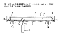
図1はワイヤボンディング法により製造した従来の半導体装置の断面図である。半導体チップ2は接着剤4を介して有機系基板6に固定されている。半導体チップの電極は、ボンディングワイヤ8により有機系基板6上に形成された電極パッド10に接続され、半導体チップ2及びボンディングワイヤ8は封止樹脂12により封止されている。また、有機系基板6の電極パッド10は、有機系基板6に形成された回路パターン(図示せず)を介して外部接続電極であるハンダボール14に電気的に接続されている。
【0008】
図1に示す半導体装置では、上述のポップコーン現象を防止するために、有機系基板6に予め複数の貫通孔であるベントホール16が形成される。ベントホール16はパンチはドリル等により形成されるため、各ベントホール16の直径は0.1μmから0.3μm程度である。このようなベントホール16が形成された有機系基板6に接着剤4を介して半導体チップ2を固定して半導体装置を形成する。
【0009】
また、ベントホール16を予め有機系基板6に形成しておくのではなく、図2に示すように、半導体チップ2を有機系基板6に固定して樹脂封止した後に、レーザ装置18を使用して有機系基板6に貫通孔を形成してベントホール16とする方法もある。
【0010】
図3はフリップチップ法により製造した従来の半導体装置の断面図である。
半導体チップ2のスタッド電極20を、有機系基板6上に形成された電極パッド10に接合することにより、半導体チップ2を有機系基板6に搭載している。半導体チップ2と有機系基板6との間にはアンダーフィル材22が充填されており、半導体チップ2は確実に有機系基板6に固定されている。また、有機系基板6の電極パッド10は、有機系基板6に形成された回路パターン(図示せず)を介して外部接続電極であるハンダボール14に電気的に接続されている。ここで、アンダーフィル材22は図1における接着剤4に相当する。
【0011】
したがって、図1に示す半導体装置と同様に、上述のポップコーン現象を防止するために、有機系基板6に予め複数の貫通孔であるベントホール16が形成される。ベントホール16はパンチ又はドリル等により形成されるため、各ベントホール16の直径は0.1μmから0.3μm程度である。このようなベントホール16が形成された有機系基板6に半導体チップ2を接合し、アンダーフィル材22を有機系基板6と半導体チップ2との間に充填して半導体装置を形成する。
【0012】
また、ベントホール16を予め有機系基板6に形成しておくのではなく、図4に示すように、半導体チップ2を有機系基板6に接合した後に、レーザ装置18を使用して有機系基板6に貫通孔を形成してベントホール16とする方法もある。
【0013】
【発明が解決しようとする課題】
図1に示した半導体装置では、有機系基板6に対して予めベントホール16が形成されているため、硬化前の液状またはペースト状の接着剤4を半導体チップ2と有機系基板6との間に供給する際に、接着剤4がベントホール16から漏出してしまうという問題があった。
【0014】
ここで、接着材4には通常フィラーが混合されているが、フィラーの粒径は50μmから60μm程度であり、ベントホール16を容易に通過してしまうため、フィラーによりベントホ−ルが塞がれることはないが、フィラーにより接着剤4の漏出を防止することもできない。
【0015】
接着剤4がベントホール16から漏出すると、漏出した接着剤が半導体装置の実装時に問題を起こすことがある。すなわち、漏出して硬化した接着剤が半導体装置の実装時に実装基板の電極等に付着し、実装時のハンダ付け不良の原因となることがある。
【0016】
上述のような接着剤の漏出による問題を回避するため、図2に示すように、接着剤4が硬化した後にベントホール16をレーザ加工により設ける。これにより、接着剤4の漏出は防止できるが、こんどは、レーザ加工により接着剤4を貫通して半導体チップ2の表面に損傷を与えるという問題が生じてしまう。近年は、半導体チップ2の厚さが薄くなっており、小さな損傷を受けただけで半導体チップ2に割れが生じてしまう。このように、半導体チップ2が損傷を受けると、半導体装置の動作不良が起こるおそれがある。
【0017】
また、図3に示す半導体装置でも、上述の図1に示す半導体装置と同様な問題が発生するおそれがある。すなわち、図3に示すように有機系基板6に予めベントホール16を形成しておいた場合は、アンダーフィル材22が漏出するという問題がある。また、図4に示すように、アンダーフィル材22が硬化した後からレーザ加工によりベントホール16を有機基板6に形成する場合は、半導体チップ2の表面に損傷を与えるおそれがある。
【0018】
特に、図3及び4に示すフリップチップ実装による半導体装置では、半導体チップ2の回路形成面が有機系基板6に面しており、レーザ加工による損傷を受ける面は回路形成面となる。したがって、ごく小さな損傷であっても、半導体チップの回路が直接影響を受け、半導体装置の動作不良を招く結果となる。
【0019】
本発明は上記の点に鑑みてなされたものであり、接着剤又はアンダーフィル材の漏出の起こらないベントホールを有する半導体装置、及びそのような半導体装置を製造する方法を提供することを目的とする。
【0020】
【課題を解決するための手段】
上記の課題は、次に述べる各手段を講じることにより解決することができる。 請求項1記載の発明は、半導体装置において、
複数の第1の貫通孔が形成された基板と、
前記基板の第1の面において前記第1の貫通孔上に形成された金属製のパターン部材であって、配線パターンに接続されないパターン部材と、
前記基板の前記第1の面及び前記パターン部材上に接着剤を介して固定された半導体素子と、
前記第1の貫通孔上の前記パターン部材に形成された第2の貫通孔と
を有し、
前記第2の貫通孔の直径は前記第1の貫通孔の直径より小さく、前記第2の貫通孔内で前記接着剤が露出していることを特徴とするものである。
【0021】
請求項2記載の発明は、請求項1記載の半導体装置であって、前記パターン部材は前記基板の前記第1の面上に形成される電極パッドと同じ材料で形成されていることを特徴とするものである。
【0022】
請求項3記載の発明は、請求項1記載の半導体装置であって、前記パター部材は前記基板の前記第1の面上に形成される回路パターンであることを特徴とするものである。
【0023】
請求項4記載の発明は、請求項1乃至3のうちいずれか一項記載の半導体装置であって、前記基板は有機材料により形成された有機系基板であることを特徴とするものである。
【0025】
上述の各手段は次のように作用する。
【0026】
請求項1記載の発明によれば、基板の第1の面に形成されたパターン部材が基板の第1の貫通孔を部分的に覆うため、第1の貫通孔の直径が第2の貫通孔の直径まで実質的に減少する。これにより、接着剤が漏出するような大きさの第1の貫通孔であっても、パターン部材の第2の貫通孔の存在により、接着剤の漏出を防止することができる。パターン部材は第1の貫通孔を部分的に覆うものであり、したがって、第1の貫通孔の一部は接着剤に対して(基板の第1の面に対して)第2の貫通孔を介して開口したままである。したがって、基板の第1の面と接着剤との界面に生じた水蒸気を第1及び第2の貫通孔を通じて逃がすことができる。
【0027】
また、請求項2記載の発明によれば、パターン部材を電極パッドと同じ材料で形成することにより、パターン部材を電極パッドと同じ工程で形成することができる。したがって、パターン部材を形成するための工程を別個に設ける必要がなく、製造コストを上昇させずに、上記請求項1記載の発明を達成実sすることができる。
【0028】
また、請求項3記載の発明によれば、パターン部材を基板の前記第1の面上に形成される回路パターンとすることにより、貫通孔を部分的に塞ぐためだけにパターン部材を設ける必要がない。すなわち、回路パターンによって、貫通孔を部分的に覆うことにより、貫通孔の実質的な大きさを減少することができ、接着剤の漏出を防止することができる。また、従来のように回路パターンを避けた位置を選んで貫通孔を設ける必要がなく、基板の設計の自由度が向上する。
【0029】
また、請求項4記載の発明によれば、有機材料により形成された有機系基板を使用して基板に貫通孔が設けられた半導体装置を構成する。有機系基板は安価であり取り扱いが簡単で加工が容易である反面、吸湿性が高いという欠点を有する。基板に吸収された水分は、接着剤と基板との間に溜まり、実装時の加熱により急激に水蒸気となって接着剤の剥離現象を引き起こす。したがって、水蒸気を逃がすための貫通孔を部分的に覆うパターン部材を有機系基板に形成することにより、有機系基板の欠点を補いながら、製造コストを上昇することなく安価に半導体装置を製造することができる。
【0031】
【発明の実施の形態】
次に、本発明の実施の形態について図面と共に説明する。
【0032】
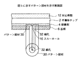
図5は本発明の第1の実施の形態による半導体装置の断面図である。図5において、図1に示す構成部品と同じ部品には同じ符号を付し、その説明は省略する。
【0033】
図5に示す半導体装置は、図1に示す半導体装置と同様に、有機系基板(以下単に基板と称する)6に複数のベントホール(貫通孔)16が予め形成されている。各ベントホールはパンチ又はドリル等により形成され、その直径は0.1μmから0.3μm程度である。このベントホール16は水蒸気を逃がすための貫通孔として機能する。
【0034】
基板6の内面、すなわち半導体チップ2に対向する面6aにはパターン部材30が設けられており、各ベントホール16はパターン部材30の下に形成されている。すなわち、各ベントホール16は対応するパターン部材30により覆われており、パターン部材30の中央にはベントホール16より小さい直径の細孔が形成されている。したがって、接着材4はパターン部材30に設けられた細孔により各ベントホール16に接続されている。
【0035】
図6は、図5においてパターン部材30が設けられた部分を拡大して示す断面図であり、パターン部材30の平面形状が合わせて示されている。図6に示すように、パターン部材30は、ベントホール16の直径より大きな直径の円形に形成されており、ベントホール16を覆うように基板6の面6aに形成されている。
【0036】
パターン部材30の中央には、上述の細孔32が設けられており、この細孔32を介して接着剤4が露出している。細孔32の直径はベントホール16の直径より十分小さく形成することができる。例えば、細孔32の直径を50μm程度とすることにより、硬化する前の液状又はペースト状の接着剤4であっても、細孔32の直径が十分小さいため、ベントホール16側に漏出することはない。
【0037】
ここで、細孔32は、水蒸気にとっては、十分大きな孔として作用し、上述のポップコーン現象が生じて水蒸気による接着材4の剥離が基板6の面6aと接着剤4との間の界面沿って広がっても、剥離がパターン部材30の細孔32に到達したところで、水蒸気は細孔32からベントホール16に逃がされることとなる。これにより、水蒸気の発生による内圧は減少し、水蒸気による剥離は細孔32を超えて広がることはない。
【0038】
したがって、多数の細孔32(ベントホール16を含む)を基板6上に設けておくことにより、ポップコーン現象が生じたとしても、小さい範囲の剥離に抑えることができ、接着剤4の剥離が半導体装置に与える影響を実質的に防止することができる。すなわち、細孔32を有するパターン部材30をベントホール16上に形成することにより、接着剤4の漏出を防止しながら接着剤4の剥離を実質的に防止することができる。
【0039】
本実施の形態では、パターン部材30は、基板6上に設けられる電極パッド10と同時に形成される。すなわち、パターン部材30は電極パッド10と同じ材料、例えば基板6の面6aに張り付けられた銅板又は銅箔をエッチングによりパターン化することにより形成される。したがって、パターン部材30は電極パッド10の形成工程において同時に形成することができ、パターン部材30を形成する工程を新たに設ける必要はない。
【0040】
パターン部材30を形成するには、まず基板6にベントホール16を形成し、ベントホール16を覆うように銅板又は銅箔を基板6の面6に貼り付ける。ベントホール16は従来と同様にパンチ又はドリルを使用して形成されるが、その直径は任意に設定可能である。すなわち、従来のように0.1μmから0.3μmの範囲としてもよく、それ以上の直径としてもよい。基板に銅板又は銅箔を貼り付けた後、銅板又は銅箔をエッチングによりパターン化し、電極パッド10とパターン部材30とを形成する。
【0041】
なお、パターン部材30の中央の細孔32は、エッチングにより形成してもよく、また、パターン部材30の形成後にレーザ加工により形成してもよい。図6に示す例では、細孔32の位置はパターン部材の中央、すなわち、ベントホール16の中央であるが、中央に限られることはなく、ベントホール16に接続されるのであれば、パターン部材30上のどの位置に形成されてもかまわない。
【0042】
また本実施の形態ではパターン部材30を電極パッド10と同じ材料により形成したが、これに限定される必要はなく、電極パッド10とは異なる材料で異なる工程において形成されてもよい。また、細孔32の直径は任意に設定することができ、使用される接着材4の粘度や混合されるフィラーの粒子径等に基づいて適当な直径を設定することが好ましい。
【0043】
また、上述の実施の形態では、ベントホール16は予め基板6に形成しておくこととしたが、細孔32を有するパターン部材30だけを予め形成しておき、ベントホール16を後からレーザ加工により形成することもできる。
【0044】
すなわち、まず、細孔32を有するパターン部材を基板6の面6aに形成し、半導体チップ2を接着剤4を介して基板6の面6aに固定してしまう。接着剤4が硬化した後で、パターン部材30が設けられた位置にレーザを照射してベントホール16を形成する。
【0045】
このような方法によれば、従来のようにレーザが接着剤4を通過してかつ半導体チップ2に損傷与えることが防止できる。レーザによりベントホール16が形成される位置には、予めパターン部材30が設けられており、基板6を除去した後に照射される余分なレーザは、パターン部材30によりほとんどが反射されてしまう。すなわち、パターン部材30は金属(銅)により形成されており、レーザを反射する性質を有している。したがって、ベントホール16が形成されてから余分に照射されるレーザは、パターン部材30により反射されて接着剤4に届くことはなく、したがって、半導体チップ2を損傷するおそれもない。
【0046】
ここで、パターン部材30には細孔32が形成されており、細孔32に照射されたレーザは僅かながら接着剤4を損傷することになる。しかし、細孔32の直径は非常に小さいため、細孔32を通過するレーザのパワーは小さく、接着剤4を貫通して半導体チップ2まで到達することはない。
【0047】
このように、パターン部材30を予め基板6に形成しておくことにより、半導体チップ2を接着在により基板6に固定した後に、レーザ加工により基板にベントホール16を形成する場合でも、照射するレーザのパワー及び、照射時間の制御を制度良く行わなくても、余分に照射されたレーザによって半導体装置2に損傷を与えることを防止できる。
【0048】
図7はパターン部材30の第1の変形例を示す断面図である。図7は図6に相当する断面図であり、パターン部材30の第1の変形例であるパターン部材30Aが設けられた部分の断面と、パターン部材30Aの平面形状が示されている。
パターン部材30Aは、正方形の形状であり、その一部がベントホール16を覆うように形成されている。ひとつのベントホール16に対して4つのパターン部材30Aが形成されており、4つのパターン部材は、所定の狭い間隙34を介して互いに隣接している。ベントホール16はこの隣接した4つのパターン部材30Aの中央に位置し、所定の狭い間隙34の部分のみパターン部材30Aに覆われないように構成されている。
【0049】
上述の構成において、図7に示す間隙34は図6に示す細孔と同様な機能を果たす。すなわち、パターン部材32Aにより部分的にベントホール16を塞いで接着剤4が漏出しないようにしつつ、ポップコーン現象が生じたときに水蒸気を間隙34を通じてベントホール16に逃がす。
【0050】
パターン部材30Aは、上述のパターン部材30と同様な工程により形成することができ、パターン部材30Aを形成するために特別に工程を設ける必要はない。したがって、コストの上昇を招くことなく、接着剤の漏出を防止しつつ接着剤の剥離を抑制した半導体装置を製造することができる。
【0051】
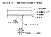
図8はパターン部材30の第2の変形例を示す断面図である。図8は図6に相当する断面図であり、パターン部材30の第2の変形例であるパターン部材30Bが設けられた部分の断面と、パターン部材30Bの平面形状が示されている。
パターン部材30Bは、いわゆる井桁状の形状であり、その一部がベントホール16を覆うように形成されている。ひとつのベントホール16に対してひとつのパターン部材30Bが形成されており、パターン部材30Bの形状により部分的にベントホール16を塞いでいる。すなわち、パターン部材32Bにより部分的にベントホール16を塞いで接着剤4が漏出しないようにしつつ、ポップコーン現象が生じたときに水蒸気を間隙パターン部材30Bにより覆われていない部分を通じてベントホール16に逃がす。
【0052】
パターン部材30Bは、上述のパターン部材30と同様な工程により形成することができ、パターン部材30Bを形成するために特別に工程を設ける必要はない。したがって、コストの上昇を招くことなく、接着剤の漏出を防止しつつ接着剤の剥離を抑制した半導体装置を製造することができる。
【0053】
なお、パターン部材30Bの形状は、図8に示された井桁形状に限ることなく、ベントホール16を適当な範囲で覆うことができるものであれば、任意の形状とすることができる。
【0054】
次に、本発明の参考例としての半導体装置について図9を参照しながら説明する。図9は本発明の参考例である半導体装置の一部を示す断面図であり、パターン部材の平面形状が合わせて示されている。図9において、図5に示す構成部品と同等な部品には同じ符号を付し、その説明は省略する。
【0055】
本参考例では、配線パターン40の一部によりベントホール16を覆うように構成している。配線パターン40は実際に電極パッド10に電気的に接続された配線パターンであり、この点で上述の第1の実施の形態とは異なる。すなわち、上述の第1の実施の形態では、配線パターン及び電極パッド10が形成されていない部分を選んでパターン部材を形成している。しかし、本参考例では、実際の配線パターン40を積極的に利用して、配線パターン40をパターン部材として使用することにより、ベントホール16を配線パターン40により部分的に覆う構成としている。
【0056】
したがって、設計の段階において、配線パターン40を基板6の面6a全面にわたって一様に配置するように設計し、ベントホール16を配線パターン40で部分的に覆われるような位置に配置する。これにより、配線パターン40を避けながらパターン部材及びベントホール16を配置する必要がなくなり、設計の自由度を向上することができる。
【0057】
図9に示す例では、互いに隣り合う配線パターン40の間の間隙を利用してベントホール16を部分的に覆う構成としている。すなわち、配線パターン40を所定の間隔で配置して、ベントホール16が配線パターン40の間に配置されるように構成している。
【0058】
上述のように、本参考例では、配線パターン40によりベントホール16を部分的に覆うことにより、ベントホール16を部分的に覆うパターン部材を別個に形成する必要がない。したがって、コストの上昇を招くことなく、接着剤の漏出を防止しつつ接着剤の剥離を抑制した半導体装置を製造することができる。
上述の本発明の第1の実施の形態及び参考例では、図1に示すような半導体チップ2をワイヤボンディグした半導体装置に関して説明したが、本発明は図3に示したような半導体チップ2をフリップチップボンディングした半導体装置にも適用できることは明らかであり、その説明は省略する。
【0059】
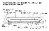
図10は、フリップチップボンディング法により製造した半導体装置に本発明を適用した場合の一例を示す図である。図10に示す半導体装置では、いわゆるスタック型の半導体装置であり、フリップチップボンディングされた半導体チップ2の上にもう一つの半導体チップ50が重ねて設けられている。上側の半導体チップ50は接着剤4により下側の半導体チップ2に固定されている。また、上側の半導体チップ50の電極は、基板6の電極パッド10にボンディングワイヤ52により接続されている。
【0060】
図11は、ワイヤボンディング法により製造した半導体装置に本発明を適用した場合の他の例を示す図である。図11に示す半導体装置では、ワイヤボンディングされた半導体チップ2の上にもう一つの半導体チップ50が重ねて設けられており、上側の半導体チップ50は接着剤4により下側の半導体チップ2に固定されている。また、上側の半導体チップ50の電極は、基板6の電極パッド10にボンディングワイヤ52によって接続されている。
【0061】
【発明の効果】
上述のように、請求項1記載の発明によれば、基板の第1の面に形成されたパターン部材が基板の第1の貫通孔を部分的に覆うため、第1の貫通孔の直径が第2の貫通孔の直径まで実質的に減少する。これにより、接着剤が漏出するような大きさの第1の貫通孔であっても、パターン部材の第2の貫通孔の存在により、接着剤の漏出を防止することができる。パターン部材は第1の貫通孔を部分的に覆うものであり、したがって、第1の貫通孔の一部は接着剤に対して(基板の第1の面に対して)第2の貫通孔を介して開口したままである。したがって、基板の第1の面と接着剤との界面に生じた水蒸気を第1及び第2の貫通孔を通じて逃がすことができる。
【0062】
また、請求項2記載の発明によれば、パターン部材を電極パッドと同じ材料で形成することにより、パターン部材を電極パッドと同じ工程で形成することができる。したがって、パターン部材を形成するための工程を別個に設ける必要がなく、製造コストを上昇させずに、上記請求項1記載の発明を達成実sすることができる。
【0063】
また、請求項3記載の発明によれば、パターン部材を基板の前記第1の面上に形成される回路パターンとすることにより、貫通孔を部分的に塞ぐためだけにパターン部材を設ける必要がない。すなわち、回路パターンによって、貫通孔を部分的に覆うことにより、貫通孔の実質的な大きさを減少することができ、接着剤の漏出を防止することができる。また、従来のように回路パターンを避けた位置を選んで貫通孔を設ける必要がなく、基板の設計の自由度が向上する。
【0064】
また、請求項4記載の発明によれば、有機材料により形成された有機系基板を使用して基板に貫通孔が設けられた半導体装置を構成する。有機系基板は安価であり取り扱いが簡単で加工が容易である反面、吸湿性が高いという欠点を有する。基板に吸収された水分は、接着剤と基板との間に溜まり、実装時の加熱により急激に水蒸気となって接着剤の剥離現象を引き起こす。したがって、水蒸気を逃がすための貫通孔を部分的に覆うパターン部材を有機系基板に形成することにより、有機系基板の欠点を補いながら、製造コストを上昇することなく安価に半導体装置を製造することができる。
【図面の簡単な説明】
【図1】 ワイヤボンディング法により製造した従来の半導体装置の断面図である。
【図2】 図1に示した半導体装置において、ベントホールをレーザ加工により形成する工程を示す断面図である。
【図3】 フリップチップボンディング法により製造した従来の半導体装置の断面図である。
【図4】 図3に示した半導体装置において、ベントホールをレーザ加工により形成する工程を示す断面図である。
【図5】 本発明の第1の実施の形態による半導体装置の断面図である。
【図6】 図5に示すパターン部材を示す断面図である。
【図7】 図6に示すパターン部材の第1の変形例を示す断面図である
【図8】 図6に示すパターン部材の第2の変形例を示す断面図である
【図9】 本発明の参考例としての半導体装置の一部の断面図である。
【図10】 本発明の実施の形態による半導体装置をスタック型とした場合の半導体装置の一例を示す断面図である。
【図11】 本発明の実施の形態による半導体装置をスタック型とした場合の半導体装置の他の例を示す断面図である。[0001]
BACKGROUND OF THE INVENTION
The present invention generally relates to semiconductor devices, and more particularly to a semiconductor device using an organic substrate formed of an organic material such as a resin material.
[0002]
Organic substrates are often used as substrates for semiconductor devices because they are inexpensive, easy to handle, and easy to process. As a typical organic substrate, there is a glass epoxy substrate or a polyimide substrate. In a semiconductor device using an organic substrate, a semiconductor chip is generally bonded and fixed to the organic substrate with an adhesive.
[0003]
However, the organic substrate has a high hygroscopic property and has a property of easily absorbing moisture in the atmosphere. If the humidity of the atmosphere is kept low during storage of the semiconductor device, the moisture absorbed by the organic substrate can be reduced. However, since the problem of static electricity may occur when the humidity is lowered, the humidity needs to be kept high to some extent.
[0004]
Therefore, organic substrates are used on the premise that they absorb a certain amount of moisture. Generally, a semiconductor using an organic substrate is provided with a means for preventing problems caused by moisture absorbed by the organic substrate. It has been.
[0005]
[Prior art]
Moisture absorbed by the organic substrate formed as a semiconductor device is accumulated at the interface between the adhesive or the underfill material for fixing the semiconductor chip on the organic substrate and the organic substrate. If such moisture rapidly evaporates due to heating during mounting of the semiconductor device, the accumulated moisture will suddenly evaporate and the internal pressure of this portion will increase, causing peeling at the interface between the adhesive and the organic substrate. There's a problem. Such peeling is called the popcorn phenomenon.
[0006]
As a measure to prevent the popcorn phenomenon, a plurality of small through-holes, generally called vent holes, are formed in the organic substrate, and water vapor generated at the interface between the adhesive and the organic substrate is passed through the through-holes in the atmosphere of the semiconductor device. The method of escaping is taken.
[0007]
FIG. 1 is a cross-sectional view of a conventional semiconductor device manufactured by a wire bonding method. The
[0008]
In the semiconductor device shown in FIG. 1,
[0009]
In addition, the
[0010]
FIG. 3 is a cross-sectional view of a conventional semiconductor device manufactured by a flip chip method.
The
[0011]
Therefore, similarly to the semiconductor device shown in FIG. 1, in order to prevent the above-described popcorn phenomenon, a plurality of
[0012]
In addition, the
[0013]
[Problems to be solved by the invention]
In the semiconductor device shown in FIG. 1, since the
[0014]
Here, filler is usually mixed in the
[0015]
If the
[0016]
In order to avoid the problem due to the leakage of the adhesive as described above, the
[0017]
Further, the semiconductor device shown in FIG. 3 may have the same problem as the semiconductor device shown in FIG. That is, when the
[0018]
In particular, in the semiconductor device by flip chip mounting shown in FIGS. 3 and 4, the circuit forming surface of the
[0019]
The present invention has been made in view of the above points, and an object thereof is to provide a semiconductor device having a vent hole in which leakage of an adhesive or an underfill material does not occur, and a method of manufacturing such a semiconductor device. To do.
[0020]
[Means for Solving the Problems]
The above problems can be solved by taking the following means. The invention according to claim 1 is a semiconductor device,
A substrate on which a plurality of first through holes are formed;
A metal pattern member formed on the first through hole on the first surface of the substrate, the pattern member not connected to the wiring pattern;
A semiconductor element fixed on the first surface of the substrate and the pattern member via an adhesive;
A second through hole formed in the pattern member on the first through hole;
Have
The diameter of the second through hole is smaller than the diameter of the first through hole, and the adhesive is exposed in the second through hole.It is characterized by this.
[0021]
According to a second aspect of the present invention, in the semiconductor device according to the first aspect, the pattern member is formed of the same material as the electrode pad formed on the first surface of the substrate. To do.
[0022]
A third aspect of the present invention is the semiconductor device according to the first aspect, wherein the putter member is a circuit pattern formed on the first surface of the substrate.
[0023]
A fourth aspect of the present invention is the semiconductor device according to any one of the first to third aspects, wherein the substrate is an organic substrate formed of an organic material.
[0025]
Each means described above operates as follows.
[0026]
According to invention of Claim 1, the pattern member formed in the 1st surface of a board | substrate is a board | substrate.FirstTo partially cover the through hole,FirstThe diameter of the through hole isUp to the diameter of the second through holeSubstantial decrease. This will allow the adhesive to leakFirstEven if it is a through hole,Of the second through holeThe presence of the adhesive can prevent leakage of the adhesive. Pattern membersFirstIt was intended to partially cover the through hole,TsuAndFirstPart of the through hole is for the adhesive (to the first surface of the substrate)Through the second through holeIt remains open. Therefore, water vapor generated at the interface between the first surface of the substrate and the adhesive is removed.First and secondIt can escape through the through hole.
[0027]
According to the second aspect of the invention, the pattern member can be formed in the same process as the electrode pad by forming the pattern member with the same material as the electrode pad. Therefore, it is not necessary to separately provide a process for forming the pattern member, and the invention of claim 1 can be achieved without increasing the manufacturing cost.
[0028]
According to the invention described in claim 3, it is necessary to provide the pattern member only for partially closing the through-hole by using the pattern member as a circuit pattern formed on the first surface of the substrate. Absent. That is, by partially covering the through hole with the circuit pattern, the substantial size of the through hole can be reduced, and leakage of the adhesive can be prevented. Further, there is no need to select a position avoiding the circuit pattern and provide a through hole as in the conventional case, and the degree of freedom in designing the substrate is improved.
[0029]
According to a fourth aspect of the present invention, a semiconductor device in which a through hole is provided in a substrate is formed using an organic substrate formed of an organic material. Organic substrates are inexpensive, easy to handle and easy to process, but have the disadvantage of high hygroscopicity. Moisture absorbed by the substrate accumulates between the adhesive and the substrate, and suddenly becomes water vapor due to heating during mounting, thereby causing a peeling phenomenon of the adhesive. Therefore, by forming a pattern member on the organic substrate that partially covers the through-hole for allowing water vapor to escape, the semiconductor device can be manufactured at low cost without increasing the manufacturing cost while compensating for the defects of the organic substrate. Can do.
[0031]
DETAILED DESCRIPTION OF THE INVENTION
Next, embodiments of the present invention will be described with reference to the drawings.
[0032]
FIG. 5 is a cross-sectional view of the semiconductor device according to the first embodiment of the present invention. 5, parts that are the same as the parts shown in FIG. 1 are given the same reference numerals, and descriptions thereof will be omitted.
[0033]
In the semiconductor device shown in FIG. 5, a plurality of vent holes (through holes) 16 are formed in advance in an organic substrate (hereinafter simply referred to as a substrate) 6 in the same manner as the semiconductor device shown in FIG. Each vent hole is formed by a punch or a drill and has a diameter of about 0.1 μm to 0.3 μm. The
[0034]
A pattern member 30 is provided on the inner surface of the
[0035]
FIG. 6 is an enlarged cross-sectional view illustrating a portion where the pattern member 30 is provided in FIG. 5, and the planar shape of the pattern member 30 is also shown. As shown in FIG. 6, the pattern member 30 is formed in a circular shape having a diameter larger than the diameter of the
[0036]
In the center of the pattern member 30, the above-described pore 32 is provided, and the adhesive 4 is exposed through the pore 32. The diameter of the pore 32 is the vent hole 16StraightIt can be formed sufficiently smaller than the diameter. For example, by setting the diameter of the pore 32 to about 50 μm, even the liquid or paste-
[0037]
Here, the pore 32 acts as a sufficiently large hole for water vapor, the above-described popcorn phenomenon occurs, and the peeling of the adhesive 4 by the water vapor occurs along the interface between the
[0038]
Therefore, by providing a large number of pores 32 (including the vent holes 16) on the
[0039]
In the present embodiment, the pattern member 30 is formed simultaneously with the
[0040]
In order to form the pattern member 30, first, the
[0041]
Pattern member30The central pore 32 may be formed by etching or a pattern.ElementYou may form by laser processing after formation of 30. In the example shown in FIG. 6, the position of the pore 32 is the center of the pattern member, that is, the center of the
[0042]
In the present embodiment, the pattern member 30 is formed of the same material as the
[0043]
In the above-described embodiment, the
[0044]
That is, first, the pattern member having the pores 32 is formed on the
[0045]
According to such a method, it is possible to prevent the laser from passing through the adhesive 4 and damaging the
[0046]
Here, pores 32 are formed in the pattern member 30, and the laser irradiated to the pores 32 slightly damages the adhesive 4. However, since the diameter of the pore 32 is very small, the power of the laser passing through the pore 32 is small and does not pass through the adhesive 4 and reach the
[0047]
As described above, by forming the pattern member 30 on the
[0048]
FIG. 7 is a cross-sectional view showing a first modification of the pattern member 30. FIG. 7 is a cross-sectional view corresponding to FIG. 6, and shows a cross section of a portion provided with a pattern member 30 </ b> A which is a first modification of the pattern member 30 and a planar shape of the pattern member 30 </ b> A.
The pattern member 30 </ b> A has a square shape, and a part thereof is formed so as to cover the
[0049]
In the above configuration, the gap 34 shown in FIG. 7 performs the same function as the pore shown in FIG. That is, the
[0050]
The
[0051]
FIG. 8 is a cross-sectional view showing a second modification of the pattern member 30. FIG. 8 is a cross-sectional view corresponding to FIG. 6, and shows a cross section of a portion provided with a pattern member 30 </ b> B, which is a second modification of the pattern member 30, and a planar shape of the pattern member 30 </ b> B.
The pattern member 30 </ b> B has a so-called cross-beam shape, and a part thereof is formed so as to cover the
[0052]
The
[0053]
The shape of the
[0054]
Next, the present inventionAs a reference exampleThe semiconductor device will be described with reference to FIG. FIG. 9 shows the present invention.Reference exampleIt is sectional drawing which shows a part of semiconductor device, and the planar shape of the pattern member is shown collectively. 9, parts that are the same as the parts shown in FIG. 5 are given the same reference numerals, and descriptions thereof will be omitted.
[0055]
BookReference
[0056]
Therefore, at the design stage, the
[0057]
In the example shown in FIG. 9, the
[0058]
As mentioned above, the bookReference exampleThen, by partially covering the
The first embodiment of the present invention described above andReference exampleIn the above, the semiconductor device in which the
[0059]
FIG. 10 is a diagram showing an example when the present invention is applied to a semiconductor device manufactured by a flip chip bonding method. The semiconductor device shown in FIG. 10 is a so-called stack type semiconductor device, and another semiconductor chip 50 is provided on the flip-chip bonded
[0060]
FIG. 11 is a diagram showing another example when the present invention is applied to a semiconductor device manufactured by a wire bonding method. In the semiconductor device shown in FIG. 11, another semiconductor chip 50 is provided over the wire-bonded
[0061]
【The invention's effect】
As described above, according to the first aspect of the present invention, the pattern member formed on the first surface of the substrate is the substrate.FirstTo partially cover the through hole,FirstThe diameter of the through hole isUp to the diameter of the second through holeSubstantial decrease. This will allow the adhesive to leakFirstEven if it is a through hole,Of the second through holeThe presence of the adhesive can prevent leakage of the adhesive. Pattern membersFirstIt was intended to partially cover the through hole,TsuAndFirstPart of the through hole is for the adhesive (to the first surface of the substrate)Through the second through holeIt remains open. Therefore, water vapor generated at the interface between the first surface of the substrate and the adhesive is removed.First and secondIt can escape through the through hole.
[0062]
According to the second aspect of the invention, the pattern member can be formed in the same process as the electrode pad by forming the pattern member with the same material as the electrode pad. Therefore, it is not necessary to separately provide a process for forming the pattern member, and the invention of claim 1 can be achieved without increasing the manufacturing cost.
[0063]
According to the invention described in claim 3, it is necessary to provide the pattern member only for partially closing the through-hole by using the pattern member as a circuit pattern formed on the first surface of the substrate. Absent. That is, by partially covering the through hole with the circuit pattern, the substantial size of the through hole can be reduced, and leakage of the adhesive can be prevented. Further, there is no need to select a position avoiding the circuit pattern and provide a through hole as in the conventional case, and the degree of freedom in designing the substrate is improved.
[0064]
According to a fourth aspect of the present invention, a semiconductor device in which a through hole is provided in a substrate is formed using an organic substrate formed of an organic material. Organic substrates are inexpensive, easy to handle and easy to process, but have the disadvantage of high hygroscopicity. Moisture absorbed by the substrate accumulates between the adhesive and the substrate, and suddenly becomes water vapor due to heating during mounting, thereby causing a peeling phenomenon of the adhesive. Therefore, by forming a pattern member on the organic substrate that partially covers the through-hole for allowing water vapor to escape, the semiconductor device can be manufactured at low cost without increasing the manufacturing cost while compensating for the defects of the organic substrate. Can do.
[Brief description of the drawings]
FIG. 1 is a cross-sectional view of a conventional semiconductor device manufactured by a wire bonding method.
2 is a cross-sectional view showing a step of forming a vent hole by laser processing in the semiconductor device shown in FIG. 1;
FIG. 3 is a cross-sectional view of a conventional semiconductor device manufactured by a flip chip bonding method.
4 is a cross-sectional view showing a step of forming a vent hole by laser processing in the semiconductor device shown in FIG. 3;
FIG. 5 is a cross-sectional view of the semiconductor device according to the first embodiment of the present invention.
6 is a cross-sectional view showing the pattern member shown in FIG.
7 is a cross-sectional view showing a first modification of the pattern member shown in FIG. 6. FIG.
FIG. 8 is a cross-sectional view showing a second modification of the pattern member shown in FIG.
FIG. 9 shows the present invention.As a reference exampleFIG. 10 is a cross-sectional view of a part of the semiconductor device.
FIG. 10 is a cross-sectional view showing an example of a semiconductor device when the semiconductor device according to the embodiment of the present invention is of a stack type.
FIG. 11 is a cross-sectional view showing another example of a semiconductor device when the semiconductor device according to the embodiment of the present invention is of a stack type.
Claims (4)
前記基板の第1の面において前記第1の貫通孔上に形成された金属製のパターン部材であって、配線パターンに接続されないパターン部材と、
前記基板の前記第1の面及び前記パターン部材上に接着剤を介して固定された半導体素子と、
前記第1の貫通孔上の前記パターン部材に形成された第2の貫通孔と
を有し、
前記第2の貫通孔の直径は前記第1の貫通孔の直径より小さく、前記第2の貫通孔内で前記接着剤が露出していることを特徴とする半導体装置。A substrate on which a plurality of first through holes are formed;
A metal pattern member formed on the first through hole on the first surface of the substrate, the pattern member not connected to the wiring pattern;
A semiconductor element fixed on the first surface of the substrate and the pattern member via an adhesive;
A second through hole formed in the pattern member on the first through hole,
The diameter of the second through hole is smaller than the diameter of the first through hole, and the adhesive is exposed in the second through hole.
Priority Applications (2)
| Application Number | Priority Date | Filing Date | Title |
|---|---|---|---|
| JP2000146850A JP4454792B2 (en) | 2000-05-18 | 2000-05-18 | Semiconductor device |
| US09/727,760 US6580173B2 (en) | 2000-05-18 | 2000-12-04 | Semiconductor device and manufacturing method of semiconductor device |
Applications Claiming Priority (1)
| Application Number | Priority Date | Filing Date | Title |
|---|---|---|---|
| JP2000146850A JP4454792B2 (en) | 2000-05-18 | 2000-05-18 | Semiconductor device |
Publications (2)
| Publication Number | Publication Date |
|---|---|
| JP2001332642A JP2001332642A (en) | 2001-11-30 |
| JP4454792B2 true JP4454792B2 (en) | 2010-04-21 |
Family
ID=18653126
Family Applications (1)
| Application Number | Title | Priority Date | Filing Date |
|---|---|---|---|
| JP2000146850A Expired - Fee Related JP4454792B2 (en) | 2000-05-18 | 2000-05-18 | Semiconductor device |
Country Status (2)
| Country | Link |
|---|---|
| US (1) | US6580173B2 (en) |
| JP (1) | JP4454792B2 (en) |
Families Citing this family (8)
| Publication number | Priority date | Publication date | Assignee | Title |
|---|---|---|---|---|
| JP2004260135A (en) * | 2003-02-06 | 2004-09-16 | Sanyo Electric Co Ltd | Semiconductor integrated device and method of manufacturing the same |
| WO2005088706A1 (en) * | 2004-02-11 | 2005-09-22 | Infineon Technologies Ag | Semiconductor package with perforated substrate |
| US7750482B2 (en) * | 2006-02-09 | 2010-07-06 | Stats Chippac Ltd. | Integrated circuit package system including zero fillet resin |
| CN103633037A (en) * | 2012-08-27 | 2014-03-12 | 国碁电子(中山)有限公司 | Encapsulation structure and manufacturing method thereof |
| US9917068B2 (en) * | 2014-03-14 | 2018-03-13 | Taiwan Semiconductor Manufacturing Company | Package substrates, packaged semiconductor devices, and methods of packaging semiconductor devices |
| US9721812B2 (en) * | 2015-11-20 | 2017-08-01 | International Business Machines Corporation | Optical device with precoated underfill |
| KR102520258B1 (en) * | 2016-03-18 | 2023-04-11 | 에스케이하이닉스 주식회사 | Semiconductor packages without mold flash and methods for fabricating the same |
| CN113284855B (en) * | 2020-02-19 | 2025-01-10 | 长鑫存储技术有限公司 | Package substrate and forming method thereof, package structure and forming method thereof |
Family Cites Families (3)
| Publication number | Priority date | Publication date | Assignee | Title |
|---|---|---|---|---|
| JP3414017B2 (en) * | 1994-12-09 | 2003-06-09 | ソニー株式会社 | Semiconductor device |
| US6242802B1 (en) * | 1995-07-17 | 2001-06-05 | Motorola, Inc. | Moisture enhanced ball grid array package |
| JPH11186294A (en) * | 1997-10-14 | 1999-07-09 | Sumitomo Metal Smi Electron Devices Inc | Semiconductor package and manufacturing method thereof |
-
2000
- 2000-05-18 JP JP2000146850A patent/JP4454792B2/en not_active Expired - Fee Related
- 2000-12-04 US US09/727,760 patent/US6580173B2/en not_active Expired - Lifetime
Also Published As
| Publication number | Publication date |
|---|---|
| JP2001332642A (en) | 2001-11-30 |
| US6580173B2 (en) | 2003-06-17 |
| US20010042908A1 (en) | 2001-11-22 |
Similar Documents
| Publication | Publication Date | Title |
|---|---|---|
| TWI413223B (en) | Package substrate embedded with semiconductor components and method of manufacturing same | |
| KR102134019B1 (en) | Substrate and semiconductor package having ball land, and the methods of fabricating the same | |
| JP2015195263A (en) | Semiconductor device and manufacturing method or the same | |
| KR20170140849A (en) | A semiconductor package and a method for manufacturing the same | |
| US20090023252A1 (en) | Method of manufacturing semiconductor device having a heat sink with a bored portion | |
| TWI611523B (en) | Semiconductor package manufacturing method | |
| CN113594051B (en) | Semiconductor packaging methods | |
| JP4454792B2 (en) | Semiconductor device | |
| JP2005101125A (en) | Semiconductor device manufacturing method, semiconductor device, circuit board, and electronic apparatus | |
| US7205485B2 (en) | Printed circuit board and method for fabricating the same | |
| JP4366666B1 (en) | Semiconductor device | |
| TW200935573A (en) | Insulative wiring board, semiconductor package using the same, and method for producing the insulative wiring board | |
| US7714417B2 (en) | Substrate for mounting semiconductor element and method of manufacturing the same | |
| EP4173448A1 (en) | Printed circuit board mesh routing to reduce solder ball joint failure during reflow | |
| KR20130009441A (en) | Semiconductor substrate, method for manufacturing semiconductor substrate and flat package chip device | |
| JP2011108814A (en) | Method of bonding surface mounting electronic component, and electronic device | |
| JP2009260165A (en) | Semiconductor device | |
| JP2015023040A (en) | Substrate structure | |
| KR20150135946A (en) | Embedded coreless substrate and method thereof | |
| JP2001127194A (en) | Flip chip type semiconductor device and manufacturing method thereof | |
| JP3029594B2 (en) | Manufacturing method of tape carrier package | |
| JP2017092328A (en) | Printed wiring board, printed wiring board manufacturing method, and semiconductor device | |
| KR20150058954A (en) | Electronic component packages and methods of manufacturing the same | |
| JPH09120976A (en) | Semiconductor chip mounting method | |
| JP5230580B2 (en) | Semiconductor device and mounting method thereof |
Legal Events
| Date | Code | Title | Description |
|---|---|---|---|
| A621 | Written request for application examination |
Free format text: JAPANESE INTERMEDIATE CODE: A621 Effective date: 20070308 |
|
| A711 | Notification of change in applicant |
Free format text: JAPANESE INTERMEDIATE CODE: A712 Effective date: 20080728 |
|
| A977 | Report on retrieval |
Free format text: JAPANESE INTERMEDIATE CODE: A971007 Effective date: 20081224 |
|
| A131 | Notification of reasons for refusal |
Free format text: JAPANESE INTERMEDIATE CODE: A131 Effective date: 20090728 |
|
| A521 | Request for written amendment filed |
Free format text: JAPANESE INTERMEDIATE CODE: A523 Effective date: 20090925 |
|
| A131 | Notification of reasons for refusal |
Free format text: JAPANESE INTERMEDIATE CODE: A131 Effective date: 20091027 |
|
| A521 | Request for written amendment filed |
Free format text: JAPANESE INTERMEDIATE CODE: A523 Effective date: 20091222 |
|
| TRDD | Decision of grant or rejection written | ||
| A01 | Written decision to grant a patent or to grant a registration (utility model) |
Free format text: JAPANESE INTERMEDIATE CODE: A01 Effective date: 20100202 |
|
| A01 | Written decision to grant a patent or to grant a registration (utility model) |
Free format text: JAPANESE INTERMEDIATE CODE: A01 |
|
| A61 | First payment of annual fees (during grant procedure) |
Free format text: JAPANESE INTERMEDIATE CODE: A61 Effective date: 20100203 |
|
| FPAY | Renewal fee payment (event date is renewal date of database) |
Free format text: PAYMENT UNTIL: 20130212 Year of fee payment: 3 |
|
| R150 | Certificate of patent or registration of utility model |
Free format text: JAPANESE INTERMEDIATE CODE: R150 |
|
| FPAY | Renewal fee payment (event date is renewal date of database) |
Free format text: PAYMENT UNTIL: 20130212 Year of fee payment: 3 |
|
| S531 | Written request for registration of change of domicile |
Free format text: JAPANESE INTERMEDIATE CODE: R313531 |
|
| S533 | Written request for registration of change of name |
Free format text: JAPANESE INTERMEDIATE CODE: R313533 |
|
| FPAY | Renewal fee payment (event date is renewal date of database) |
Free format text: PAYMENT UNTIL: 20130212 Year of fee payment: 3 |
|
| R350 | Written notification of registration of transfer |
Free format text: JAPANESE INTERMEDIATE CODE: R350 |
|
| FPAY | Renewal fee payment (event date is renewal date of database) |
Free format text: PAYMENT UNTIL: 20140212 Year of fee payment: 4 |
|
| S111 | Request for change of ownership or part of ownership |
Free format text: JAPANESE INTERMEDIATE CODE: R313111 |
|
| R350 | Written notification of registration of transfer |
Free format text: JAPANESE INTERMEDIATE CODE: R350 |
|
| LAPS | Cancellation because of no payment of annual fees |