JP4454530B2 - Power factor correction circuit - Google Patents
Power factor correction circuit Download PDFInfo
- Publication number
- JP4454530B2 JP4454530B2 JP2005116962A JP2005116962A JP4454530B2 JP 4454530 B2 JP4454530 B2 JP 4454530B2 JP 2005116962 A JP2005116962 A JP 2005116962A JP 2005116962 A JP2005116962 A JP 2005116962A JP 4454530 B2 JP4454530 B2 JP 4454530B2
- Authority
- JP
- Japan
- Prior art keywords
- voltage
- current
- power supply
- switching element
- switching
- Prior art date
- Legal status (The legal status is an assumption and is not a legal conclusion. Google has not performed a legal analysis and makes no representation as to the accuracy of the status listed.)
- Expired - Fee Related
Links
- 238000004804 winding Methods 0.000 claims description 39
- 239000003990 capacitor Substances 0.000 claims description 29
- 238000001514 detection method Methods 0.000 claims description 20
- 230000000694 effects Effects 0.000 description 4
- 230000007423 decrease Effects 0.000 description 3
- 238000010586 diagram Methods 0.000 description 3
- 229910044991 metal oxide Inorganic materials 0.000 description 2
- 150000004706 metal oxides Chemical class 0.000 description 2
- 238000000034 method Methods 0.000 description 2
- 102100024237 Stathmin Human genes 0.000 description 1
- 108050003387 Stathmin Proteins 0.000 description 1
- 230000002411 adverse Effects 0.000 description 1
- 230000003247 decreasing effect Effects 0.000 description 1
- 238000012544 monitoring process Methods 0.000 description 1
- 230000001360 synchronised effect Effects 0.000 description 1
- 230000007704 transition Effects 0.000 description 1
Images


Classifications
-
- Y—GENERAL TAGGING OF NEW TECHNOLOGICAL DEVELOPMENTS; GENERAL TAGGING OF CROSS-SECTIONAL TECHNOLOGIES SPANNING OVER SEVERAL SECTIONS OF THE IPC; TECHNICAL SUBJECTS COVERED BY FORMER USPC CROSS-REFERENCE ART COLLECTIONS [XRACs] AND DIGESTS
- Y02—TECHNOLOGIES OR APPLICATIONS FOR MITIGATION OR ADAPTATION AGAINST CLIMATE CHANGE
- Y02P—CLIMATE CHANGE MITIGATION TECHNOLOGIES IN THE PRODUCTION OR PROCESSING OF GOODS
- Y02P80/00—Climate change mitigation technologies for sector-wide applications
- Y02P80/10—Efficient use of energy, e.g. using compressed air or pressurized fluid as energy carrier
Landscapes
- Rectifiers (AREA)
- Dc-Dc Converters (AREA)
Description
本発明は、スイッチング電源に用いられる力率改善回路に関する。 The present invention relates to a power factor correction circuit used for a switching power supply.
従来、以下に述べる臨界動作型のスイッチング電源の例として、特許文献1に、零電流検出回路に、抵抗、コンデンサ、ダイオードからなるインピーダンス回路を内蔵し、交流入力電圧の実効値が低い場合にもスイッチング素子をオン状態に維持することにより、設計の自由度を広くし、スイッチング素子のディレーティングを改善することができるスイッチング電源装置が記載されている。
図4に示す、従来におけるスイッチング電源2は、後述するように、トランスT1の補助巻線Ncから抵抗R4を介して、力率改善回路(Power Factor Correction Circuit)12の入力端Bに、スイッチング素子であるMOS−FET(Metal Oxide Semiconductor−Field Effect Transistor)Q1がオフ期間にトランスT1の1次巻線Npに流れる電流がゼロになったことを示すz/c(zero/current)信号を出力し、力率改善回路12はMOS−FETQ1のオフ状態を検出し、該オフの状態への移行を確認して、MOS−FETQ1のゲートに駆動信号(オントリガ)を出力することにより、MOS−FETQ1を一旦オフの状態に移行させて、1次巻線Npに流れる電流がゼロになってからオンの状態に移行させている。このように、MOS−FETQ1を一旦オフの状態に移行させてからオンの状態に移行させるスイッチング電源2を電流臨界型のスイッチング電源という。
As shown later, the conventional switching power supply 2 shown in FIG. 4 has a switching element connected to an input terminal B of a power
ところで、スイッチング電源には、上述したような電流臨界型のスイッチング電源の他に、スイッチング素子のスイッチング周期毎にインダクタ電流をゼロまで戻さずに制御を行う電流連続型のスイッチング電源が存在する。ここで、電流臨界型のスイッチング電源および電流連続型のスイッチング電源が有する短所について説明する。 By the way, in addition to the current critical switching power supply as described above, there is a continuous current switching power supply that performs control without returning the inductor current to zero every switching cycle of the switching element. Here, the disadvantages of the current critical switching power supply and the continuous current switching power supply will be described.
電流臨界型スイッチング電源は、低い入力電圧に対して、大きい出力電力を取り出すとき、スイッチング電源のスイッチング周波数が低くなって可聴帯域内に入り、チョークのハウリングが発生してしまう。また、スイッチング素子およびチョークに流れる電流のピークの値が大きくなり、効率が低下することもあり、大電力用には不向きである。 In a current critical switching power supply, when a large output power is taken out with respect to a low input voltage, the switching frequency of the switching power supply is lowered to enter the audible band, and choke howling occurs. In addition, the peak value of the current flowing through the switching element and choke becomes large and the efficiency may be lowered, which is not suitable for high power use.
一方、電流連続型のスイッチング電源は、スイッチング素子のスイッチングロスが大きいため、小電力用としては、電流臨界型のスイッチング電源に対して、効率が低下してしまう。これは、電流臨界型のスイッチング電源においてはスイッチング電流の波形が三角形になるのに対し、電流連続型のスイッチング電源においてはスイッチング素子がオンした瞬間、スイッチング電流が急激に上昇し、その後、ゆっくり上昇して、無駄にスイッチング電流が流れ、スイッチング損失が増大するためである。 On the other hand, since the continuous current type switching power supply has a large switching loss of the switching element, the efficiency decreases for the low power use as compared with the current critical type switching power supply. This is because the waveform of the switching current is triangular in the current critical type switching power supply, whereas in the continuous current type switching power supply, the switching current suddenly rises at the moment when the switching element is turned on, and then rises slowly. This is because a switching current flows unnecessarily and switching loss increases.
以上のように、電流臨界型のスイッチング電源および電流連続型のスイッチング電源は、使用する電力の大きさによって、それぞれ得失があり、一般に、出力電力が300W程度までの小さな電源としては電流臨界型のスイッチング電源が使用され、300W以上の大電力の電源としては電流連続型のスイッチング電源が使用される。よって、電流臨界型か電流連続型かのスイッチング電源の動作形態の選択は、一般的に、出力電力の大きさによってなされ、該選択に基づいて、異なる制御用IC(Integrated Circuit)を設計して使用している。このために、回路規模が大型化するという問題があった。 As described above, the current critical switching power supply and the current continuous switching power supply have their advantages and disadvantages depending on the amount of power used. In general, the current critical switching power supply has a current critical type as a small power supply with an output power of about 300 W. A switching power supply is used, and a continuous current type switching power supply is used as a high-power power supply of 300 W or more. Therefore, the selection of the operation mode of the current critical type or the continuous current type switching power supply is generally made according to the magnitude of the output power, and different control ICs (Integrated Circuits) are designed based on the selection. I use it. For this reason, there has been a problem that the circuit scale increases.
本発明は、上記事情を考慮してなされたもので、その目的は、スイッチング電源において、回路規模を大きくすることなく、全負荷領域において、高効率化を図ることができる力率改善回路を提供することにある。 The present invention has been made in view of the above circumstances, and an object of the present invention is to provide a power factor correction circuit capable of achieving high efficiency in the entire load region without increasing the circuit scale in a switching power supply. There is to do.
上記目的を達成するために、この発明では、以下の手段を提案している。
請求項1に係る発明は、交流電圧を整流して供給する整流手段と、1次巻線および2次巻線を有し、前記1次巻線の一端が前記整流手段と接続されたトランスと、前記トランスの1次巻線の他端と接続されたスイッチング素子とに接続され、前記スイッチング素子によって、前記交流電圧の周期に比して速い周期にて繰り返しオン・オフして、前記整流手段の出力電力の制御を行う力率改善回路であって、前記スイッチング素子に流れる電流を検出するスイッチング素子電流検出手段と、前記2次巻線に接続され、前記スイッチング素子がオフ期間に1次巻線に流れる電流がゼロになったことを検出するゼロ電流検出手段と、前記スイッチング素子の出力電圧を検出する出力電圧検出手段と、前記スイッチング素子がオン・オフするための電圧および前記ゼロ電流検出手段の検出結果に基づいて、前記スイッチング素子をオフする時間を設定するオフ時間設定手段とを備えたことを特徴とする。
この発明によれば、スイッチング素子電流検出手段およびゼロ電流検出手段の検出結果に基づいて、スイッチング素子をオフする時間を設定するオフ時間設定手段を設けることにより、スイッチング素子のオフ時間を設定して、スイッチング電源を電流臨界型のスイッチング電源から電流連続型のスイッチング電源へ移行させ、回路規模を大きくすることなく、大電力を取り出せるスイッチング電源を提供することができる。
In order to achieve the above object, the present invention proposes the following means.
The invention according to
According to the present invention, the off time of the switching element is set by providing the off time setting means for setting the time to turn off the switching element based on the detection results of the switching element current detecting means and the zero current detecting means. The switching power supply can be shifted from the current critical switching power supply to the continuous current switching power supply, and a switching power supply that can extract a large amount of power without increasing the circuit scale can be provided.
請求項2に係る発明は、請求項1に記載の力率改善回路であって、前記オフ時間設定手段が、所定の時定数をなす抵抗およびコンデンサからなる時定数回路と、前記スイッチング素子がオン・オフするための電圧および前記ゼロ電流検出手段の検出結果および前記所定の時定数に基づいて、前記コンデンサを充電する充電手段とを備えることを特徴とする。
この発明によれば、時定数回路の定数を変更して時定数を変更することにより、スイッチング電源を電流臨界型のスイッチング電源から電流連続型のスイッチング電源へ移行させるときの出力電力値を変更することができる。
The invention according to claim 2 is the power factor correction circuit according to
According to the present invention, the output power value when changing the switching power supply from the current critical switching power supply to the current continuous switching power supply is changed by changing the time constant by changing the constant of the time constant circuit. be able to.
請求項1に係る発明によれば、回路規模を大きくすることなく、全負荷領域において、スイッチング電源1の高効率化を図ることができる効果がある。また、請求項2に係る発明によれば、抵抗およびコンデンサの値の変更により、オフ時間設定動作の領域を簡単に変更することができる効果がある。
According to the first aspect of the invention, there is an effect that the switching
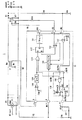
図1に示すように、本発明の一実施形態におけるスイッチング電源1は、ダイオードブリッジDB1(整流手段)と、トランスT1と、スイッチング素子であるMOS−FET(Metal Oxide Semiconductor−Field Effect Transistor)Q1と、ダイオードD1と、コンデンサC1、C13と、抵抗R1〜10と、力率改善回路11とから構成される。本実施形態においては、スイッチング電源1は、入力端ACinputにおいてコンセントから交流100〜200Vを入力し、出力端outputにおいて直流380Vを出力する。
尚、本実施形態におけるスイッチング電源1は、図4に示す、従来におけるスイッチング電源2に比して、力率改善回路12が、入力端Fとグランド電位との間に抵抗R11およびコンデンサC11(時定数回路)を外付けし、MOS−FETQ1をオン・オフさせるための電圧およびz/c信号の電圧を監視し、該電圧に基づいてMOS−FETQ1のオフ時間を設定するオフ時間設定回路118(オフ時間設定手段)およびオア(Or)ゲート119(オフ時間設定手段)を内部に追加した構成の力率改善回路11に置き換えられているところが異なる。
As shown in FIG. 1, a
In the
ダイオードブリッジDB1は整流回路をなし、コンセントから入力した交流電力を整流する。トランスT1は、チョークとも呼ばれ、磁気コアに巻き回され、且つ、相互に電磁結合された1次巻線Np、補助巻線(2次巻線または制御巻線)Ncを有する。ここで、1次巻線Npの“p”は“primary”の頭の文字から、補助巻線Ncの“c”は、“control”の頭の文字からとられている。MOS−FETQ1は、第1および第2の主端子としてドレインとソースおよび制御電極としてゲートを有する。尚、MOS−FETQ1は、ゲートにハイレベルの信号が入力されるとドレインとソースとが電気的に導通する。 The diode bridge DB1 forms a rectifier circuit and rectifies AC power input from an outlet. The transformer T1, also called a choke, has a primary winding Np and an auxiliary winding (secondary winding or control winding) Nc wound around a magnetic core and electromagnetically coupled to each other. Here, “p” of the primary winding Np is taken from the initial letter “primary”, and “c” of the auxiliary winding Nc is taken from the initial letter “control”. The MOS-FET Q1 has a drain and a source as first and second main terminals and a gate as a control electrode. In the MOS-FET Q1, the drain and the source are electrically connected when a high level signal is input to the gate.
入力端ACInputの内の一方の端は、ダイオードブリッジDB1の一方の交流入力端に接続される。入力端ACInputの内の他方の端はダイオードブリッジDB1の他方の交流入力端に接続される。ダイオードブリッジDB1の正の直流出力端が抵抗R1の一方の端に接続される。抵抗R1の他方の端はコンデンサC1の一方の端、トランスT1の1次巻線Npの負極側および抵抗R2の一方の端に接続される。 One end of the input end ACInput is connected to one AC input end of the diode bridge DB1. The other end of the input terminals ACInput is connected to the other AC input terminal of the diode bridge DB1. The positive DC output terminal of the diode bridge DB1 is connected to one terminal of the resistor R1. The other end of the resistor R1 is connected to one end of the capacitor C1, the negative side of the primary winding Np of the transformer T1, and one end of the resistor R2.
トランスT1の1次巻線Npの正極側がMOS−FETQ1のドレインおよびダイオードD1のアノードに接続される。ダイオードD1のカソードが電解コンデンサからなるコンデンサC13の正極側および出力端Outputの内の正電圧端+Vならびに抵抗R8の一方の端に接続される。 The positive side of the primary winding Np of the transformer T1 is connected to the drain of the MOS-FET Q1 and the anode of the diode D1. The cathode of the diode D1 is connected to the positive side of the capacitor C13 made of an electrolytic capacitor, the positive voltage end + V of the output end Output, and one end of the resistor R8.
ダイオードブリッジDB1の負の直流出力端がコンデンサC1の他方の端、抵抗R6、R7の一方の端、コンデンサC13の負極側および出力端Outputの内の負電圧端−Vに接続される。 The negative DC output terminal of the diode bridge DB1 is connected to the other terminal of the capacitor C1, one terminal of the resistors R6 and R7, the negative electrode side of the capacitor C13, and the negative voltage terminal -V of the output terminal Output.
抵抗R2の他方の端は、抵抗R3の一方の端および力率改善回路11の入力端Aに接続される。抵抗R3の他方の端はグランド電位に接地される。尚、抵抗R2およびR3は入力側分圧抵抗をなす。
The other end of the resistor R2 is connected to one end of the resistor R3 and the input end A of the power
トランスT1の補助巻線Ncの負極側はグランド電位に接地される。トランスT1の補助巻線Ncの正極側は抵抗R4の一方の端に接続される。抵抗R4の他方の端は力率改善回路11の入力端Bに接続される。MOS−FETQ1のソースは抵抗R7の他方の端および抵抗R10を介して力率改善回路11の入力端Cに接続される。尚、抵抗R7はMOS−FETQ1のスイッチング電流IQ1を検出するための電流検出用の抵抗である。
The negative side of the auxiliary winding Nc of the transformer T1 is grounded to the ground potential. The positive side of the auxiliary winding Nc of the transformer T1 is connected to one end of the resistor R4. The other end of the resistor R4 is connected to the input end B of the power
抵抗R8の他方の端は、抵抗R9の一方の端および力率改善回路11の入力端Dに接続される。抵抗R9の他方の端はグランド電位に接地される。尚、抵抗R8およびR9は出力側分圧抵抗をなす。
The other end of the resistor R8 is connected to one end of the resistor R9 and the input end D of the power
MOS−FETQ1のゲートは抵抗R5の一方の端および抵抗R6の他方の端に接続される。抵抗R5の他方の端は力率改善回路11の出力端Eに接続される。
The gate of the MOS-FET Q1 is connected to one end of the resistor R5 and the other end of the resistor R6. The other end of the resistor R5 is connected to the output end E of the power
力率改善回路11は、ドライバ111と、コンパレータ112(スイッチング素子電流検出手段)と、マルチプライヤ113(入力電圧検出手段)と、RSフリップフロップ(Reset-Set Flip-Flop)115と、コンパレータ116(ゼロ電流検出手段)、コンパレータ117(出力電圧検出手段)と、ワンショット・マルチバイブレータ(OSMV:単安定マルチバイブレータ)120と、定電圧源E16,E17とから構成され、入力端A〜Dにて入力した諸信号に基づいてMOS−FETQ1をオン・オフするための電圧VGSを生成して出力端Eから出力し、スイッチング電源1の制御回路として動作する。また、力率改善回路11は、スイッチング電源1において、後述するように、内蔵しているオフ時間設定回路118およびオアゲート119によって、MOS−FETQ1をオン・オフさせるための電圧およびz/c信号の電圧に基づいて、スイッチング電源1を前述した電流臨界型のスイッチング電源として動作させるか、電流連続型のスイッチング電源として動作させるかを選択して、全負荷領域においてスイッチング電源1の高効率化を図る。
The power
マルチプライヤ113の一方の入力端は力率改善回路11の入力端Aに接続される。定電圧源E17の正出力端はコンパレータ117の正入力端に接続され、定電圧源E17の負出力端はグランド電位に接地される。コンパレータ117の負入力端は力率改善回路11の入力端Dに接続される。マルチプライヤ113の他方の入力端はコンパレータ117の出力端に接続される。コンパレータ112の負入力端はマルチプライヤ113の出力端に接続される。コンパレータ112の正入力端は力率改善回路11の入力端Cに接続され、コンパレータ112の出力端はRSフリップフロップ115の入力端Rに接続される。
One input terminal of the
定電圧源E16の正出力端はコンパレータ116の負入力端に接続され、定電圧源E16の負出力端はグランド電位に接地される。コンパレータ116の正入力端は力率改善回路11の入力端Bに接続され、コンパレータ116の出力端はOSMV120の入力端に接続される。OSMV120の出力端はオアゲート119の一方の入力端に接続される。オアゲート119の出力端はRSフリップフロップ115の入力端Sに接続される。RSフリップフロップ115の出力端Qはドライバ111の入力端に接続され、ドライバ111の出力端は力率改善回路11の出力端Eに接続される。
The positive output terminal of the constant voltage source E16 is connected to the negative input terminal of the
マルチプライヤ113は入力端Aから入力した電圧MULTと、コンパレータ117による、入力端Dから入力した電圧と定電圧源E17の出力電圧との比較結果とを乗算してコンパレータ112へ出力する。コンパレータ112は入力端Cから入力した電圧と、マルチプライヤ113から入力した乗算結果とを比較して、比較結果をRSフリップフロップ115の入力端Rに出力する。
The
コンパレータ116は、入力端Bから入力した電圧と定電圧源E16の出力電圧との比較結果とを比較して比較結果をOSMV120に出力する。OSMV120は一定のレベルを保つ信号またはローレベルからハイレベルに上がる信号を入力した場合、ローレベルの信号を、オアゲート119を介してRSフリップフロップ115の入力端Sに出力するが、ハイレベルからローレベルに下がる信号を入力した場合、該信号の立下り以前はローレベルであり、立ち上がりに同期して一定時間長だけハイレベルとなり、その後ローレベルに戻る信号(パルス)を、オアゲート119を介してRSフリップフロップ115の入力端Sに出力する。
The
RSフリップフロップ115は入力端RまたはSに入力された電圧に基づいて、出力端Qについて、セット動作またはリセット動作を行う。ドライバ111は、例えば、トランジスタを用いたスイッチング回路から構成され、RSフリップフロップ115の出力端Qの電圧に基づいて、スイッチング電源1に入力される交流電流の周波数より高い周波数(スイッチング周波数)にて、MOS−FETQ1をオン・オフさせる。ドライバ111はハイレベルの信号を入力するとMOS−FETQ1をオンさせ、ローレベルの信号を入力するとMOS−FETQ1をオフさせる。尚、ドライバ111は、上述したように、MOS−FETQ1のゲートをオン・オフさせることができればどんなものでもよい。
The RS flip-
オフ時間設定回路118の入力端Ip18aはMOS−FETQ1のゲート端子およびドライバ111の出力端に接続される。オフ時間設定回路118の入力端Ip18bはOSMV120の出力端およびオアゲート119の一方の入力端に接続される。オフ時間設定回路118の入力端Ip18cは力率改善回路11の入力端Fを介して抵抗R11の一方の端およびコンデンサC11の一方の端に接続される。抵抗R11の他方の端およびコンデンサC11の他方の端はグランド電位に接地される。オフ時間設定回路118の出力端Op18はオアゲート119の他方の入力端に接続される。尚、MOS−FETQ1のゲート信号と同期していれば、入力端Ip18aはドライバ111の入力端に接続してもよい。
The input terminal Ip18a of the off
オフ時間設定回路118は、コンパレータ181(充電手段)と、オアゲート182(充電手段)と、ノット(Not)ゲート183(充電手段)と、定電圧源E18と、定電流源Ires18(充電手段)と、MOS−FETQ18(充電手段)とから構成される。
The off-
オフ時間設定回路118の入力端Ip18aはオアゲート182の三つのうちの一つの入力端に接続される。オフ時間設定回路118の入力端Ip18bはオアゲート182の残りの二つのうちの一つの入力端に接続される。オフ時間設定回路118の出力端Op18はオアゲート182の残りの一つの入力端およびコンパレータ181の出力端に接続される。オアゲート182の出力端はノットゲート183を介してMOS−FETQ18のゲートに接続される。定電流源Ires18の負出力端は基準電源電圧Vrefに接続される。定電流源Ires18の正出力端はMOS−FETQ18のソースに接続される。オフ時間設定回路118の入力端Ip18cはMOS−FETQ18のドレインおよびコンパレータ181の負入力端に接続される。コンパレータ181の正入力端は定電圧源E18の正出力端に接続される。定電圧源E18の負出力端はグランド電位に接地される。
The input terminal Ip18a of the off
次に、スイッチング電源1の動作を説明する。
先ず、MOS−FETQ1が力率改善回路11によってオンしているとすると、入力端ACinputから入力された交流電流がダイオードブリッジDB1によって整流され、整流された直流電流が、抵抗R1、トランスT1の一次巻線Np、MOS−FETQ1および抵抗R7を通じて流れ、一次巻線Npに電磁エネルギが蓄積される。
Next, the operation of the switching
First, assuming that the MOS-FET Q1 is turned on by the power
次に、MOS−FETQ1が力率改善回路11によってオフし、一次巻線Npに蓄積された電磁エネルギが放出されて、ダイオードD1およびコンデンサC13に電流が流れ、コンデンサC13が昇圧充電される。これにより、入力端ACinputから入力された交流電圧より高い値の直流出力電圧がコンデンサC13の両端から、出力端outputにおいて出力される。
Next, the MOS-FET Q1 is turned off by the power
そして、一次巻線Npに流れる電流(インダクタ電流)が徐々に減少してゼロまで戻る制御が行われる。このように、MOS−FETQ1のスイッチング周期毎にインダクタ電流をゼロに戻す制御を行うスイッチング電源を、電流臨界型のスイッチング電源という。 Then, control is performed in which the current (inductor current) flowing through the primary winding Np gradually decreases and returns to zero. A switching power supply that performs control to return the inductor current to zero every switching period of the MOS-FET Q1 is referred to as a current critical switching power supply.
次に、力率改善回路11の動作の概略を説明する。
先ず、ここで、MOS−FETQ1がオンしているとする。入力端Aにおいて、ダイオードブリッジDB1から出力された直流電圧を抵抗R2およびR3によって分圧した電圧である電圧MULTが入力され、入力端Dにおいて、出力端outputにおける直流電圧を抵抗R8およびR9によって分圧した電圧である電圧MOが入力され、コンパレータ117において定電圧源E17の出力電圧と比較され、コンパレータ117の出力電圧と電圧MULTがマルチプライヤ113によって乗算されて、交流入力電流の基準信号が生成される。そして、該基準信号の電圧と抵抗R7の検出電圧とがコンパレータ112によって比較される。このとき、抵抗R7の検出電圧が基準電圧より大きいと、コンパレータ112はハイレベルの信号をRSフリップフロップ115の入力端Rに出力し、RSフリップフロップ115の出力端Qからローレベルの信号を出力させ(リセットする)、ドライバ111を介して、MOS−FETQ1をオフにする。
Next, an outline of the operation of the power
First, here, it is assumed that the MOS-FET Q1 is turned on. At the input terminal A, a voltage MULT that is a voltage obtained by dividing the DC voltage output from the diode bridge DB1 by the resistors R2 and R3 is input. At the input terminal D, the DC voltage at the output terminal output is divided by the resistors R8 and R9. A voltage MO, which is a compressed voltage, is input and compared with the output voltage of the constant voltage source E17 in the
以上のように、MOS−FETQ1がオンからオフの状態になると、抵抗R7に以下のような電圧が発生する。すなわち、MOS−FETQ1のVDSとグランド電位との差の電圧が発生する。それに伴い、一次巻線Npにも同様の電圧が発生し、巻線比に比例して、補助巻線Ncにも電圧が発生し、抵抗R4を介して、力率改善回路11の入力端Bにおいて、z/c(zero/current)信号として観測される。以上の動作により、補助巻線Ncによって、力率改善回路11において、MOS−FETQ1のオフ期間に1次巻線Npに流れる電流がゼロになったことを検知することができる。ここで、1次巻線Npに流れる電流がゼロになると、補助巻線Ncの電圧が負になり、z/c信号もローレベルになり、z/c信号の電圧が定電圧源E16の出力電圧より小さくなり、コンパレータ116はローレベルの信号をOSMV120に出力し、OSMV120が規定のハイレベルの信号を発して、オアゲート119を介して、RSフリップフロップ115の入力端Sに出力し、RSフリップフロップ115の出力端Qからハイレベルの信号を出力させ(セットする)、ドライバ111を介して、MOS−FETQ1をオンにする。以上の動作により、力率改善回路11によってMOS−FETQ1のオン・オフ制御が行われることになる。
As described above, when the MOS-FET Q1 is turned from on to off, the following voltage is generated in the resistor R7. That is, a difference voltage between the VDS of the MOS-FET Q1 and the ground potential is generated. Accordingly, a similar voltage is generated in the primary winding Np, and a voltage is also generated in the auxiliary winding Nc in proportion to the winding ratio. The input terminal B of the power
次に、力率改善回路11の動作の詳細を説明する。
先ず、力率改善回路11がMOS−FETQ1のオン・オフ制御を一定周期にて行う場合について説明する。力率改善回路11ではなく、コンデンサインプット型電源のとき、入力端ACinputにおいて流れる電流は、急峻に変化するパルス状の電流となる。
Next, details of the operation of the power
First, the case where the power
ここで、電力は電圧と電流の積であるから、時間的に見て、電圧と電流との積である電力がゼロとなる領域が広くなり、電力を効率的に取り出すことが難しくなる。これを、「力率が悪化する」という。また、電流の波形が急峻に変化するため、電気的なノイズを発生して、他の機器の動作に悪影響を与えてしまう。 Here, since the electric power is a product of the voltage and the current, a region where the electric power that is the product of the voltage and the current becomes zero is widened in time, and it is difficult to efficiently extract the electric power. This is called "power factor worsens". In addition, since the current waveform changes sharply, electrical noise is generated, which adversely affects the operation of other devices.
そのため、MOS−FETQ1に、以下のような条件を満たすようなスイッチング電流IQ1を流す。すなわち、スイッチング電流IQ1のピーク値によって形成される包絡線Evr1、換言すると、入力端ACinputにおいて流れる電流が、入力端ACinputにおいて印加される電圧と同じ波形を有するようにする。 Therefore, a switching current IQ1 that satisfies the following condition is passed through the MOS-FET Q1. That is, the envelope Evr1 formed by the peak value of the switching current IQ1, in other words, the current flowing at the input terminal ACinput has the same waveform as the voltage applied at the input terminal ACinput.
具体的に、MOS−FETQ1に上述したようなスイッチング電流IQ1を流すためには、以下のような動作を行う。すなわち、スイッチング電流IQ1が右上がりの傾斜を有する領域においては、MOS−FETQ1がオンして、スイッチング電流IQ1が増加している状況であり、スイッチング電流IQ1が右下がりがりの傾斜を有する領域においては、MOS−FETQ1のオフ期間になって、スイッチング電流IQ1が減少している状況である。そのため、MOS−FETQ1をオンする時間長さを調整することによって、スイッチング電流IQ1のピーク値を調整する。 Specifically, in order to pass the switching current IQ1 as described above to the MOS-FET Q1, the following operation is performed. That is, in the region where the switching current IQ1 has an upward slope, the MOS-FET Q1 is turned on and the switching current IQ1 is increasing. In the region where the switching current IQ1 has an upward slope, In this state, the switching current IQ1 is decreasing due to the off-period of the MOS-FET Q1. Therefore, the peak value of the switching current IQ1 is adjusted by adjusting the time length for turning on the MOS-FET Q1.
ここで、MOS−FETQ1をオンするための信号(オントリガ)は補助巻線Ncによって検出され、入力端Bにおいて入力されるz/c信号に基づいて生成される。一方、MOS−FETQ1をオフするための信号(オフトリガ)は、入力端Aにおいて入力される電圧MULT、入力端Dにおいて入力される電圧MOおよびMOS−FETQ1に流れるスイッチング電流IQ1に比例する電圧CSに基づいて生成される。これらのオントリガ、オフトリガは、出力端Eから電圧VGSとして出力される。 Here, a signal (on trigger) for turning on the MOS-FET Q1 is detected by the auxiliary winding Nc and is generated based on the z / c signal inputted at the input terminal B. On the other hand, the signal (off trigger) for turning off the MOS-FET Q1 is a voltage MULT inputted at the input terminal A, a voltage MO inputted at the input terminal D, and a voltage CS proportional to the switching current IQ1 flowing through the MOS-FET Q1. Based on. These on-trigger and off-trigger are output from the output terminal E as the voltage VGS.
以上の動作によって、力率改善回路11は、力率を向上させつつ、MOS−FETQ1をオン・オフし、且つ、周りの電気機器に対する影響を軽減する。これらのことより、MOS−FETQ1のオン・オフ制御を行う回路を、「力率改善回路」という。
With the above operation, the power
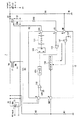
次に、オフ時間設定回路118の動作を、図2を参照して説明する。
先ず、交流入力電圧が100V系である場合のオフ時間設定回路118の動作の概略について説明する。オフ時間設定回路118は、図2(a)に示すように、抵抗R11およびコンデンサC11によって決まる時定数をパルス幅とするスイッチング波形を、オアゲート119を介してRSフリップフロップ115に出力し、MOS−FETQ1のオン・オフ制御を行う。また、オフ時間設定回路118は、入力端Ip18aおよびIp18bから入力した電圧VGSおよびz/c信号の電圧とにも基づいて、スイッチング波形を、オアゲート119を介してRSフリップフロップ115に出力し、MOS−FETQ1のオン・オフ制御を行う。
Next, the operation of the off-
First, an outline of the operation of the off-
次に、オフ時間設定回路118の動作の詳細を、図2を参照して説明する。
まず、MOS−FETQ1をオン・オフさせるための電圧VGSはローレベルになっている。時刻t0において、図2(a)に示す、入力端Ip18bにおけるスイッチング波形がハイレベルに移行すると、オアゲート182は、いずれかの入力端にハイレベルの信号が入力されるため、ハイレベルの信号を出力し、オアゲート182の出力端に接続されているノットゲート183にローレベルの信号を出力させ、MOS−FETQ18をオンさせる。そして、定電流源Ires18からコンデンサC11に充電電流が供給され、図2(b)に示すように、電圧VToffが上昇し、基準電源電圧Vrefと等しくなったところで、電圧の上昇が停止する。そして、時刻t1において、スイッチング波形がローレベルになるために、オアゲート182にローレベルの信号が入力され、ノットゲート183を介してMOS−FETQ18をオフさせ、コンデンサC11の充電を停止させる。そして、コンデンサC11は抵抗R11によって放電され、電圧VToffは下降する。
Next, details of the operation of the off-
First, the voltage VGS for turning on / off the MOS-FET Q1 is at a low level. When the switching waveform at the input terminal Ip18b shown in FIG. 2A shifts to a high level at time t0, the
そして、時刻t2において、電圧VToffが予め定められた値まで下降すると、コンパレータ181は、ハイレベルのスイッチング波形を出力し、RSフリップフロップ115のセットが入り、トランスT1の1次巻線Npの電流がゼロになる前にMOS−FETQ1をオンさせるため、電流連続型として動作する。このとき、コンデンサC11を充電する。
At time t2, when the voltage VToff drops to a predetermined value, the comparator 181 outputs a high-level switching waveform, the RS flip-
そして、図2(c)に示すように、時刻t3において、電圧VToffが低電圧源E18の出力電圧までに下がる前に、トランスT1の補助巻線Ncからz/c信号が入力されると、電流臨界型として動作する、このとき、OSMV120は、z/c信号の立下りに同期して、一定時間ハイレベルとなるパルスをオフ時間設定回路118の入力端Ip18bに出力する。ここで、オアゲート182のいずれかの入力端にハイレベルの信号が入力されるので、前述したように、コンパレータ181は、ハイレベルのスイッチング波形を出力し、前述した手順にてコンデンサC11を充電する。
As shown in FIG. 2 (c), when the z / c signal is input from the auxiliary winding Nc of the transformer T1 before the voltage VToff drops to the output voltage of the low voltage source E18 at time t3, At this time, the
次に、時刻t4〜t5において、マルチプライヤ113が、スイッチング電源1に200V系の電源入力されていることを認識すると、オアゲート182のいずれかの入力端に図2(d)に示すタイミングにて、時刻t4〜t5において、オフ設定解除信号として、ハイレベルの信号が入力され、前述したように、コンパレータ181は、ハイレベルのスイッチング波形を出力し、前述した手順にてコンデンサC11を充電する、そして、電圧VToffが基準電源電圧Vrefに等しくなっても、コンデンサC11の充電動作が停止しないため、コンデンサC11は放電されず、タイマは停止する。
Next, at time t4 to t5, when the
次に、電流臨界型のスイッチング電源と電流連続型のスイッチング電源の出力電流の波形について説明する。図3(a)は電流臨界型のスイッチング電源の出力電流の波形を示し、図3(b)は、図3(a)の拡大図である。図3(a)および、図3(b)に示すように、電流波形はゼロとある値との間を往復している。 Next, waveforms of output currents of the current critical switching power supply and the continuous current switching power supply will be described. FIG. 3A shows the waveform of the output current of the current critical switching power supply, and FIG. 3B is an enlarged view of FIG. As shown in FIG. 3A and FIG. 3B, the current waveform reciprocates between zero and a certain value.
一方、図3(c)はオフ時間固定による電流連続型のスイッチング電源の出力電流の波形を示し、図3(d)は、図3(c)の拡大図である。図3(b)および、図3(d)に示すように、電流波形は二つのゼロでない値とある値との間を往復している。尚、図3(d)は、図3(c)における区間tについての拡大図である。 On the other hand, FIG. 3C shows the waveform of the output current of the continuous current switching power supply with the fixed off time, and FIG. 3D is an enlarged view of FIG. As shown in FIGS. 3B and 3D, the current waveform reciprocates between two non-zero values and a certain value. FIG. 3D is an enlarged view of the section t in FIG.
ここで、電流臨界型のスイッチング電源と電流連続型のスイッチング電源の出力電流の波形について比較を行うと、次のことがいえる。すわなち、図3(a)(b)の波形と図3(c)(d)の波形とを比較すると、図3(c)(d)の方が電流のピーク値が低く、効率がよいことがわかる。 Here, when the waveforms of the output currents of the current critical switching power supply and the continuous current switching power supply are compared, the following can be said. That is, when comparing the waveforms in FIGS. 3A and 3B with the waveforms in FIGS. 3C and 3D, the peak values of the currents are lower in FIGS. 3C and 3D, and the efficiency is higher. I know it ’s good.
上記実施形態によれば、力率改善回路11を、従来のスイッチング電源1に使用される力率改善回路11内に、MOS−FETQ1をオン・オフさせるための電圧およびz/c信号の電圧を監視し、該電圧に基づいてMOS−FETQ1のオフ時間を設定するオフ時間設定回路118を設けた構成とし、且つ、オフ時間設定回路118を、出力電力に応じて動作させ、スイッチング電源1を電流臨界型のスイッチング電源として動作させるか、電流連続型のスイッチング電源として動作させるか否かを選択する。したがって、回路規模を大きくすることなく、全負荷領域において、スイッチング電源1の高効率化を図ることができる。
According to the above-described embodiment, the power
また、上記実施形態によれば、オフ時間設定回路118のオフ時間設定動作は、オフ時間設定回路118に外付けされる抵抗R11およびコンデンサC11によって決まる時定数にしたがって行われるので、抵抗R11およびコンデンサC11の値の変更により、オフ時間設定動作の領域を簡単に変更することができる。
Further, according to the above embodiment, the off time setting operation of the off
以上、本発明の実施形態について図面を参照して詳述したが、具体的な構成はこの実施形態に限られるものではなく、本発明の要旨を逸脱しない範囲での設計変更も含まれる。 As mentioned above, although embodiment of this invention was explained in full detail with reference to drawings, the concrete structure is not restricted to this embodiment, The design change in the range which does not deviate from the summary of this invention is also included.
1、2・・・スイッチング電源、11、12・・・力率改善回路(Power Factor Correction Circuit)、111・・・ドライバ、112・・コンパレータ(スイッチング素子電流検出手段)、113・・・マルチプライヤ(入力電圧検出手段)、115・・・RSフリップフロップ(Reset-Set Flip-Flop)、116・・・コンパレータ(ゼロ電流検出手段)、117・・・コンパレータ(出力電圧検出手段)、118・・・オフ時間設定回路(オフ時間設定手段)、119・・・オア(Or)ゲート(オフ時間設定手段)、120・・・ワンショット・マルチバイブレータ(OSMV:単安定マルチバイブレータ)、181・・・コンパレータ(充電手段)、182・・・オアゲート(充電手段)、183・・・ノット(Not)ゲート(充電手段)
DESCRIPTION OF
Claims (2)
前記スイッチング素子に流れる電流を検出するスイッチング素子電流検出手段と、
前記2次巻線に接続され、前記スイッチング素子がオフ期間に1次巻線に流れる電流がゼロになったことを検出するゼロ電流検出手段と、
前記スイッチング素子の出力電圧を検出する出力電圧検出手段と、
前記スイッチング素子がオン・オフするための電圧および前記ゼロ電流検出手段の検出結果に基づいて、前記スイッチング素子をオフする時間を設定するオフ時間設定手段と、
を備えたことを特徴とする力率改善回路。 Rectifying means for rectifying and supplying AC voltage, a primary winding and a secondary winding, one end of the primary winding being connected to the rectifying means, and a primary winding of the transformer Is connected to a switching element connected to the other end of the switch, and is repeatedly turned on and off at a cycle faster than the cycle of the AC voltage by the switching element to control the output power of the rectifying means. A rate improvement circuit,
Switching element current detecting means for detecting a current flowing through the switching element;
Zero current detecting means connected to the secondary winding and detecting that the current flowing through the primary winding during the off period of the switching element becomes zero;
Output voltage detecting means for detecting the output voltage of the switching element;
Off time setting means for setting a time for turning off the switching element based on a voltage for turning on and off the switching element and a detection result of the zero current detecting means;
A power factor correction circuit characterized by comprising:
所定の時定数をなす抵抗およびコンデンサからなる時定数回路と、
前記スイッチング素子がオン・オフするための電圧および前記ゼロ電流検出手段の検出結果および前記所定の時定数に基づいて、前記コンデンサを充電する充電手段と、
を備えることを特徴とする請求項1に記載の力率改善回路。
The off-time setting means is
A time constant circuit composed of a resistor and a capacitor having a predetermined time constant;
Charging means for charging the capacitor based on a voltage for turning on and off the switching element, a detection result of the zero current detection means, and the predetermined time constant;
The power factor correction circuit according to claim 1, comprising:
Priority Applications (1)
| Application Number | Priority Date | Filing Date | Title |
|---|---|---|---|
| JP2005116962A JP4454530B2 (en) | 2005-04-14 | 2005-04-14 | Power factor correction circuit |
Applications Claiming Priority (1)
| Application Number | Priority Date | Filing Date | Title |
|---|---|---|---|
| JP2005116962A JP4454530B2 (en) | 2005-04-14 | 2005-04-14 | Power factor correction circuit |
Publications (2)
| Publication Number | Publication Date |
|---|---|
| JP2006296158A JP2006296158A (en) | 2006-10-26 |
| JP4454530B2 true JP4454530B2 (en) | 2010-04-21 |
Family
ID=37416114
Family Applications (1)
| Application Number | Title | Priority Date | Filing Date |
|---|---|---|---|
| JP2005116962A Expired - Fee Related JP4454530B2 (en) | 2005-04-14 | 2005-04-14 | Power factor correction circuit |
Country Status (1)
| Country | Link |
|---|---|
| JP (1) | JP4454530B2 (en) |
Families Citing this family (8)
| Publication number | Priority date | Publication date | Assignee | Title |
|---|---|---|---|---|
| JP2008187821A (en) * | 2007-01-30 | 2008-08-14 | Matsushita Electric Works Ltd | Insulated ac-dc converter and dc power supply unit for led using it |
| JP4963068B2 (en) * | 2007-02-06 | 2012-06-27 | 新電元工業株式会社 | Power factor correction circuit |
| JP5326804B2 (en) | 2008-09-29 | 2013-10-30 | 富士電機株式会社 | Power factor improving power supply device, control circuit used for power supply device, and control method |
| JP5277952B2 (en) * | 2008-12-25 | 2013-08-28 | 富士電機株式会社 | Switching power supply circuit |
| JP5332766B2 (en) * | 2009-03-16 | 2013-11-06 | 富士電機株式会社 | Switching power supply circuit |
| DE112010003631T5 (en) * | 2009-10-29 | 2014-12-11 | Fuji Electric Co., Ltd. | Switching power supply circuit and power factor control |
| KR101171597B1 (en) * | 2010-11-01 | 2012-08-06 | 서울시립대학교 산학협력단 | Apparatus of detecting zero-inductor-current for switching type voltage converter |
| CN108718154B (en) * | 2018-05-30 | 2019-11-12 | 苏州博创集成电路设计有限公司 | The adjusting circuit of Switching Power Supply constant voltage output |
-
2005
- 2005-04-14 JP JP2005116962A patent/JP4454530B2/en not_active Expired - Fee Related
Also Published As
| Publication number | Publication date |
|---|---|
| JP2006296158A (en) | 2006-10-26 |
Similar Documents
| Publication | Publication Date | Title |
|---|---|---|
| TWI423569B (en) | Isolated flyback converter with efficient light load operation | |
| US8665614B2 (en) | Control method and device for switching power supplies having more than one control mode | |
| JP4963068B2 (en) | Power factor correction circuit | |
| US8031490B2 (en) | Power supply circuit and power supply system | |
| KR101769130B1 (en) | Power supply, apparatus and method for controlling link voltage control switch | |
| JP3116338B2 (en) | Switching power supply | |
| JP5489502B2 (en) | Power supply | |
| US20150280574A1 (en) | System and Method for a Switched-Mode Power Supply | |
| KR20100117980A (en) | Power factor correction circuit and driving method thereof | |
| JPWO2006101135A1 (en) | Switching power supply circuit | |
| JP4155211B2 (en) | Switching power supply | |
| KR101858059B1 (en) | Switch control circuit, power factor corrector comprising the same, and driving mehtod of the power factor corrector | |
| JP4454530B2 (en) | Power factor correction circuit | |
| JP6908849B2 (en) | Synchronous rectifier circuit and switching power supply | |
| JP2016178800A (en) | Switching power supply | |
| CN103703662B (en) | Buffer circuit | |
| JP2007511995A (en) | Switch mode power supply | |
| US9431920B2 (en) | Non-isolated DC/DC converter with 2 inductors and zero voltage switching | |
| EP1260014B1 (en) | Switched mode power supply | |
| JP4111326B2 (en) | Switching power supply | |
| JP4919858B2 (en) | Switching power supply | |
| WO2007123098A1 (en) | Switching power supply circuit and its control method | |
| JP6253200B2 (en) | Switching power supply | |
| JP2004194412A (en) | Switching power supply, switching control apparatus, and control method of the switching power supply | |
| JP4718773B2 (en) | converter |
Legal Events
| Date | Code | Title | Description |
|---|---|---|---|
| A621 | Written request for application examination |
Free format text: JAPANESE INTERMEDIATE CODE: A621 Effective date: 20070523 |
|
| TRDD | Decision of grant or rejection written | ||
| A01 | Written decision to grant a patent or to grant a registration (utility model) |
Free format text: JAPANESE INTERMEDIATE CODE: A01 Effective date: 20100112 |
|
| A01 | Written decision to grant a patent or to grant a registration (utility model) |
Free format text: JAPANESE INTERMEDIATE CODE: A01 |
|
| A61 | First payment of annual fees (during grant procedure) |
Free format text: JAPANESE INTERMEDIATE CODE: A61 Effective date: 20100202 |
|
| FPAY | Renewal fee payment (event date is renewal date of database) |
Free format text: PAYMENT UNTIL: 20130212 Year of fee payment: 3 |
|
| R150 | Certificate of patent or registration of utility model |
Ref document number: 4454530 Country of ref document: JP Free format text: JAPANESE INTERMEDIATE CODE: R150 Free format text: JAPANESE INTERMEDIATE CODE: R150 |
|
| FPAY | Renewal fee payment (event date is renewal date of database) |
Free format text: PAYMENT UNTIL: 20130212 Year of fee payment: 3 |
|
| FPAY | Renewal fee payment (event date is renewal date of database) |
Free format text: PAYMENT UNTIL: 20140212 Year of fee payment: 4 |
|
| LAPS | Cancellation because of no payment of annual fees |