JP4155211B2 - Switching power supply - Google Patents
Switching power supply Download PDFInfo
- Publication number
- JP4155211B2 JP4155211B2 JP2004057786A JP2004057786A JP4155211B2 JP 4155211 B2 JP4155211 B2 JP 4155211B2 JP 2004057786 A JP2004057786 A JP 2004057786A JP 2004057786 A JP2004057786 A JP 2004057786A JP 4155211 B2 JP4155211 B2 JP 4155211B2
- Authority
- JP
- Japan
- Prior art keywords
- synchronous rectifier
- voltage
- circuit
- winding
- switching element
- Prior art date
- Legal status (The legal status is an assumption and is not a legal conclusion. Google has not performed a legal analysis and makes no representation as to the accuracy of the status listed.)
- Expired - Lifetime
Links
- 230000001360 synchronised effect Effects 0.000 claims description 149
- 238000004804 winding Methods 0.000 claims description 113
- 238000001514 detection method Methods 0.000 claims description 53
- 239000003990 capacitor Substances 0.000 claims description 36
- 238000009499 grossing Methods 0.000 claims description 27
- 230000005284 excitation Effects 0.000 claims description 13
- 238000010586 diagram Methods 0.000 description 9
- 230000007423 decrease Effects 0.000 description 7
- 230000000694 effects Effects 0.000 description 6
- 230000003071 parasitic effect Effects 0.000 description 6
- 230000002411 adverse Effects 0.000 description 3
- 238000000034 method Methods 0.000 description 3
- 230000015556 catabolic process Effects 0.000 description 2
- 238000007599 discharging Methods 0.000 description 2
- 230000000087 stabilizing effect Effects 0.000 description 2
- 230000003111 delayed effect Effects 0.000 description 1
- 230000007613 environmental effect Effects 0.000 description 1
- 230000004048 modification Effects 0.000 description 1
- 238000012986 modification Methods 0.000 description 1
- 230000002441 reversible effect Effects 0.000 description 1
- 230000006641 stabilisation Effects 0.000 description 1
- 238000011105 stabilization Methods 0.000 description 1
Images


Classifications
-
- H—ELECTRICITY
- H02—GENERATION; CONVERSION OR DISTRIBUTION OF ELECTRIC POWER
- H02M—APPARATUS FOR CONVERSION BETWEEN AC AND AC, BETWEEN AC AND DC, OR BETWEEN DC AND DC, AND FOR USE WITH MAINS OR SIMILAR POWER SUPPLY SYSTEMS; CONVERSION OF DC OR AC INPUT POWER INTO SURGE OUTPUT POWER; CONTROL OR REGULATION THEREOF
- H02M3/00—Conversion of dc power input into dc power output
- H02M3/22—Conversion of dc power input into dc power output with intermediate conversion into ac
- H02M3/24—Conversion of dc power input into dc power output with intermediate conversion into ac by static converters
- H02M3/28—Conversion of dc power input into dc power output with intermediate conversion into ac by static converters using discharge tubes with control electrode or semiconductor devices with control electrode to produce the intermediate ac
- H02M3/325—Conversion of dc power input into dc power output with intermediate conversion into ac by static converters using discharge tubes with control electrode or semiconductor devices with control electrode to produce the intermediate ac using devices of a triode or a transistor type requiring continuous application of a control signal
- H02M3/335—Conversion of dc power input into dc power output with intermediate conversion into ac by static converters using discharge tubes with control electrode or semiconductor devices with control electrode to produce the intermediate ac using devices of a triode or a transistor type requiring continuous application of a control signal using semiconductor devices only
- H02M3/33569—Conversion of dc power input into dc power output with intermediate conversion into ac by static converters using discharge tubes with control electrode or semiconductor devices with control electrode to produce the intermediate ac using devices of a triode or a transistor type requiring continuous application of a control signal using semiconductor devices only having several active switching elements
- H02M3/33576—Conversion of dc power input into dc power output with intermediate conversion into ac by static converters using discharge tubes with control electrode or semiconductor devices with control electrode to produce the intermediate ac using devices of a triode or a transistor type requiring continuous application of a control signal using semiconductor devices only having several active switching elements having at least one active switching element at the secondary side of an isolation transformer
- H02M3/33592—Conversion of dc power input into dc power output with intermediate conversion into ac by static converters using discharge tubes with control electrode or semiconductor devices with control electrode to produce the intermediate ac using devices of a triode or a transistor type requiring continuous application of a control signal using semiconductor devices only having several active switching elements having at least one active switching element at the secondary side of an isolation transformer having a synchronous rectifier circuit or a synchronous freewheeling circuit at the secondary side of an isolation transformer
-
- H—ELECTRICITY
- H02—GENERATION; CONVERSION OR DISTRIBUTION OF ELECTRIC POWER
- H02M—APPARATUS FOR CONVERSION BETWEEN AC AND AC, BETWEEN AC AND DC, OR BETWEEN DC AND DC, AND FOR USE WITH MAINS OR SIMILAR POWER SUPPLY SYSTEMS; CONVERSION OF DC OR AC INPUT POWER INTO SURGE OUTPUT POWER; CONTROL OR REGULATION THEREOF
- H02M3/00—Conversion of dc power input into dc power output
- H02M3/22—Conversion of dc power input into dc power output with intermediate conversion into ac
- H02M3/24—Conversion of dc power input into dc power output with intermediate conversion into ac by static converters
- H02M3/28—Conversion of dc power input into dc power output with intermediate conversion into ac by static converters using discharge tubes with control electrode or semiconductor devices with control electrode to produce the intermediate ac
-
- Y—GENERAL TAGGING OF NEW TECHNOLOGICAL DEVELOPMENTS; GENERAL TAGGING OF CROSS-SECTIONAL TECHNOLOGIES SPANNING OVER SEVERAL SECTIONS OF THE IPC; TECHNICAL SUBJECTS COVERED BY FORMER USPC CROSS-REFERENCE ART COLLECTIONS [XRACs] AND DIGESTS
- Y02—TECHNOLOGIES OR APPLICATIONS FOR MITIGATION OR ADAPTATION AGAINST CLIMATE CHANGE
- Y02B—CLIMATE CHANGE MITIGATION TECHNOLOGIES RELATED TO BUILDINGS, e.g. HOUSING, HOUSE APPLIANCES OR RELATED END-USER APPLICATIONS
- Y02B70/00—Technologies for an efficient end-user side electric power management and consumption
- Y02B70/10—Technologies improving the efficiency by using switched-mode power supplies [SMPS], i.e. efficient power electronics conversion e.g. power factor correction or reduction of losses in power supplies or efficient standby modes
Description
本発明は、トランスを有すると共に、トランスの二次巻線から出力される電力を同期整流器を利用して整流する回路を備えたスイッチング電源装置に関するものである。 The present invention relates to a switching power supply apparatus having a transformer and a circuit for rectifying power output from a secondary winding of the transformer using a synchronous rectifier.
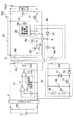
従来から、出力電圧を間接的に検出する検出回路を設け、この検出回路の検出結果に基づいてメインスイッチング素子をPWM方式により制御するスイッチング電源装置が提案されている(例えば特許文献1参照)。図9は、そのような検出回路を備えたスイッチング電源装置の主要な構成部分の一回路構成例を表す図である。 2. Description of the Related Art Conventionally, a switching power supply device has been proposed in which a detection circuit that indirectly detects an output voltage is provided and a main switching element is controlled by a PWM method based on a detection result of the detection circuit (see, for example, Patent Document 1). FIG. 9 is a diagram illustrating a circuit configuration example of main components of the switching power supply device including such a detection circuit.
このスイッチング電源装置200はトランス1を有し、このトランス1の一次巻線N1にはメインスイッチング素子(MOSFET)Q1が接続され、このトランス1とメインスイッチング素子Q1の直列接続回路は、入力フィルタ6を介して外部の入力電源5に接続されている。
This switching
トランス1の二次巻線N2には二次側整流平滑回路20が接続されている。この二次側整流平滑回路20は、二次巻線N2に直列に接続される第1の同期整流器(スイッチング素子(MOSFET))Q2と、二次巻線N2に並列に接続される第2の同期整流器(スイッチング素子(MOSFET))Q3と、二次巻線N2に並列に接続されているチョークコイル21とコンデンサ22の直列接続回路とを有して構成されている。この二次側整流平滑回路20は、二次巻線N2の出力電力を、同期整流器Q2,Q3のスイッチング動作によって整流し、また、チョークコイル21とコンデンサ22によって平滑して、直流電圧Voutを外部の負荷に向けて出力する。
A secondary side rectifying and smoothing
同期整流器Q3のスイッチング制御用端子(ゲート端子)には第2同期整流器駆動回路25が接続されており、この第2同期整流器駆動回路25は、同期整流器Q3が、メインスイッチング素子Q1のスイッチオン・オフ動作とは逆のスイッチオン・オフ動作を行うように同期整流器Q3のスイッチング動作を制御する。つまり、第2同期整流器駆動回路25によって、メインスイッチング素子Q1がオフのときには同期整流器Q3はオンし、メインスイッチング素子Q1がオンのときには同期整流器Q3はオフする。
A second synchronous
また、同期整流器Q2は、二次巻線N2の誘起電圧によって、メインスイッチング素子Q1のスイッチオン・オフ動作と同じスイッチオン・オフ動作を行う。 The synchronous rectifier Q2 performs the same switch on / off operation as the switch on / off operation of the main switching element Q1 by the induced voltage of the secondary winding N2.
トランス1には三次巻線N3が設けられており、この三次巻線N3には検出回路30が接続されている。検出回路30は、三次巻線N3に誘起された電圧を整流する整流素子であるダイオード31,32と、その電圧を平滑するチョークコイル33とコンデンサ34と、整流平滑された電圧を分圧する分圧抵抗体35,36とを有して構成されている。三次巻線N3には、二次巻線N2に誘起される電圧に応じた電圧が誘起されることから、検出回路30は、その三次巻線N3の誘起電圧を整流平滑することで、二次側整流平滑回路20から負荷に出力される出力電圧Voutを間接的に検出し当該出力電圧Voutの検出電圧を出力している。
The
メインスイッチング素子Q1のスイッチング制御用端子であるゲート端子には制御回路10が接続されている。制御回路10は、検出回路30による出力電圧Voutの検出電圧に基づきPWM方式によりメインスイッチング素子Q1のスイッチオン・オフ動作を制御する回路であり、誤差増幅器11と、基準電圧源12と、比較器13と、三角波信号発振器14とを有して構成されている。つまり、制御回路10では、検出回路30による出力電圧Voutの検出電圧と、基準電圧源12から出力された基準電圧との誤差電圧が誤差増幅器11によって増幅される。そして、比較器13によって、その増幅電圧と、三角波信号発振器14から出力される三角波信号との大きさが比較され、当該比較結果に基づいたスイッチング制御用の信号(パルス信号)がメインスイッチング素子Q1のゲート端子に加えられる。そのスイッチング制御用の信号がハイレベルである場合にはメインスイッチング素子Q1はオンし、スイッチング制御用の信号がローレベルである場合にはメインスイッチング素子Q1はオフする。このように、二次側整流平滑回路20の出力電圧Voutを間接的に検出する検出回路30の検出結果に基づき制御回路10によってメインスイッチング素子Q1のスイッチング制御が行われる。
A
以下に、スイッチング電源装置200の主要な回路構成部分の動作例を図10の波形例を利用して述べる。
Hereinafter, an operation example of main circuit components of the switching
例えば、制御回路10の制御動作によってメインスイッチング素子Q1がオンしているときには(例えば図10に示すON期間)、入力電源5から入力電圧Vinが入力し当該入力電圧Vinは入力フィルタ6により平滑されて一次巻線N1に供給される。これにより、二次巻線N2には電圧が誘起され、この二次巻線N2の誘起電圧によって同期整流器Q2がオンする(図10(d)参照)。また、第2同期整流器駆動回路25によって同期整流器Q3がオフする(図10(c)参照)。これら同期整流器Q2,Q3のスイッチング動作によって、二次側には、二次巻線N2の誘起電圧に基づいた電流が、二次巻線N2→負荷→チョークコイル21→同期整流器Q2→二次巻線N2の電流ループでもって通電して負荷に出力電圧Voutが出力される。この電流通電によってチョークコイル21には励磁エネルギーが蓄積される。
For example, when the main switching element Q1 is turned on by the control operation of the control circuit 10 (for example, the ON period shown in FIG. 10), the input voltage Vin is input from the
また、このメインスイッチング素子Q1のON期間に、検出回路30には、三次巻線N3の誘起電圧(図10(e)参照)に基づいた電流が、三次巻線N3→分圧抵抗体36→分圧抵抗体35→チョークコイル33→ダイオード32→三次巻線N3の電流ループでもって通電して、検出回路30から出力電圧Voutの検出電圧が制御回路10に出力される。この電流通電によってチョークコイル33には出力電圧Voutに応じた励磁エネルギーが蓄積される。
Also, the ON period of the main switching element Q1, a
メインスイッチング素子Q1がオフしているときには(例えば図10に示すOFF期間)、同期整流器Q2がオフし、同期整流器Q3はオンする。これにより、チョークコイル21に蓄積されていた励磁エネルギーの電流が、チョークコイル21→同期整流器Q3→負荷→チョークコイル21の電流ループでもって通電して負荷に出力電圧Voutが出力される。このとき、検出回路30には、チョークコイル33の励磁エネルギーに基づいた出力電圧Voutの検出電流がチョークコイル33とダイオード31と分圧抵抗体36と分圧抵抗体35を通る電流ループでもって通電して、検出回路30から出力電圧Voutの検出電圧が出力される。
When the main switching element Q1 is off (for example, the OFF period shown in FIG. 10), the synchronous rectifier Q2 is turned off and the synchronous rectifier Q3 is turned on. As a result, the current of the excitation energy accumulated in the
ところで、メインスイッチング素子Q1がスイッチオフすると、図10のB期間に示されるように、一次巻線N1の励磁エネルギーに基づいて、一次巻線N1と、メインスイッチング素子Q1の寄生容量とによる共振が行われる。この共振動作が終了してからメインスイッチング素子Q1がスイッチオンするまでの期間(A期間)には、同期整流器Q2のドレイン−ソース間に寄生ダイオード(ボディダイオード)23があるために、二次巻線N2の励磁を維持すべく、二次巻線N2の励磁電流が、同期整流器Q2のボディダイオード23→二次巻線N2→同期整流器Q3→ボディダイオード23の電流ループでもって通電する。この二次巻線N2の励磁電流は、チョークコイル21を通らないため、出力電圧Voutには全く関係ない電流である。
By the way, when the main switching element Q1 is switched off, as shown in the period B of FIG. 10, resonance by the primary winding N1 and the parasitic capacitance of the main switching element Q1 is caused based on the excitation energy of the primary winding N1. Done. During the period (A period) from the end of the resonance operation to the time when the main switching element Q1 is switched on, there is a parasitic diode (body diode) 23 between the drain and source of the synchronous rectifier Q2. In order to maintain the excitation of the line N2, the exciting current of the secondary winding N2 is energized through the current loop of the
上記のようにボディダイオード23を介して二次巻線N2に電流が通電すると、ボディダイオード23の電圧降下に応じた電圧が二次巻線N2に誘起される。二次巻線N2と三次巻線N3は磁気結合していることから、A期間中には、その二次巻線N2の誘起電圧に応じた電圧VN3Aが三次巻線N3に誘起される(例えば図10(e)参照)。この三次巻線N3の誘起電圧VN3Aに基づいた電流は、チョークコイル33→ダイオード32→三次巻線N3→分圧抵抗体36→分圧抵抗体35→チョークコイル33の電流ループでもって通電するので、チョークコイル33の励磁エネルギーに基づいた出力電圧Voutの検出電流に重畳されることになる。
As described above, when a current flows through the secondary winding N2 via the
なお、同期整流器Q2のボディダイオード23の電圧降下をVfとし、二次巻線N2の巻回数をN2とし、三次巻線N3の巻回数をN3とした場合には、メインスイッチング素子Q1のOFF期間中のA期間(一次側の共振動作が終了してからメインスイッチング素子Q1がスイッチオンするまでの期間)に三次巻線N3に誘起される電圧VN3Aは、VN3A=Vf×(N3/N2)の数式で表すことができる。この誘起電圧VN3Aが発生しているA期間中に、検出回路30には、その誘起電圧VN3Aに基づいた電流と、チョークコイル33の励磁エネルギーに基づいた出力電圧Voutの検出電流とが通電するので、検出回路30で整流される電圧は、チョークコイル33の両端電圧と、ダイオード32の電圧降下量と、三次巻線N3の誘起電圧VN3Aとが加算された電圧となるが、通常、制御回路10のインピーダンスは、検出回路30のインピーダンスよりもはるかに高いために、A期間中のチョークコイル33の両端電圧は、B期間中のチョークコイル33の両端電圧よりも、同期整流器Q2のボディダイオード23の電圧降下に起因した三次巻線N3の誘起電圧VN3A分だけ低くなる(例えば図10(f)参照)。
When the voltage drop of the
メインスイッチング素子Q1のOFF期間中のA期間において、三次巻線N3の誘起電圧VN3Aに基づいて検出回路30を通電する電流は、二次巻線N2の励磁エネルギーに対応する電流であり、当該電流は出力電圧Voutには関与しない電流であることから、この電流が、チョークコイル33の励磁エネルギーに基づいた出力電圧Voutの検出電流に重畳されることによって、検出回路30から出力電圧Voutの正確な検出電圧を得ることができないという問題が発生する。同期整流器Q2のオフ期間中のボディダイオード23の電圧降下Vfは、オン期間中の電圧降下に比べてかなり大きいので、A期間中に、検出回路30の出力電圧Voutの検出電流に重畳される前記電流は無視できないものであり、検出回路30の出力電圧Voutの検出精度を低下させている。
In the period A during the OFF period of the main switching element Q1, the current flowing through the
メインスイッチング素子Q1のOFF期間中におけるA期間は、入力電圧Vinが高くなるにつれて長くなり、A期間が長くなる程、検出回路30の出力電圧Voutの検出精度が悪くなる。このため、検出回路30の検出電圧に基づいた制御回路10によるメインスイッチング素子Q1のスイッチング制御によって、負荷への出力電圧Voutが低くなる。また、同期整流器Q2のボディダイオード23の電圧降下Vfは、周囲の環境温度が低くなるに従って大きくなるので、周囲の環境温度が低くなるにつれて、検出回路30の出力電圧Voutの検出精度が悪くなって負荷への出力電圧Voutが低くなる。図11のグラフ中の実線aに示されるように、入力電圧Vinの大小や、周囲温度の変動に拘わらず、出力電圧Voutが一定である出力電圧特性を持つことが望ましいが、図9に示すスイッチング電源装置200の構成では、A期間におけるボディダイオード23の電圧降下に起因した問題によって、図11のグラフ中の点線b,c,dに示されるように、入力電圧Vinが高くなるに従って出力電圧Voutが低下し、また、周囲温度が低くなるに従って入力電圧Vinの変動量に対する出力電圧Voutの変化量が大きくなるという出力電圧特性となってしまう。
The A period during the OFF period of the main switching element Q1 becomes longer as the input voltage Vin becomes higher, and the detection accuracy of the output voltage Vout of the
なお、同期整流器Q2のドレイン−ソース間に外付けのダイオードが設けられる場合があり、この場合にも、上記同様の問題が発生する。 Note that an external diode may be provided between the drain and source of the synchronous rectifier Q2, and in this case, the same problem as described above occurs.
本発明は上記課題を解決するために成されたものであり、その目的は、メインスイッチング素子のOFF期間において、二次巻線に直列に接続された同期整流器のボディダイオードあるいは外付けのダイオードに起因した出力電圧Voutの検出電圧の不正確さを改善して、出力電圧Voutの高精度な安定化制御を行うことができるスイッチング電源装置を提供することにある。 The present invention has been made to solve the above-mentioned problems, and its purpose is to provide a synchronous rectifier body diode or an external diode connected in series with the secondary winding in the OFF period of the main switching element. It is an object of the present invention to provide a switching power supply apparatus that can improve the inaccuracy of the detected voltage of the output voltage Vout caused by this and perform highly accurate stabilization control of the output voltage Vout.
上記目的を達成するために、この発明は次に示す構成をもって前記課題を課題を解決するための手段としている。すなわち、この発明は、トランスと、トランスの一次巻線に接続されているメインスイッチング素子と、このメインスイッチング素子のスイッチオン・オフ動作に基づいてトランスの二次巻線から出力される電力を整流平滑して外部に出力する二次側整流平滑回路と、トランスの三次巻線に誘起される電圧を利用して二次側整流平滑回路の出力電圧を間接的に検出する検出回路と、この検出回路による出力電圧の検出電圧に基づき二次側整流平滑回路の出力電圧の安定化を図るべくメインスイッチング素子のスイッチオン・オフ動作を制御する制御回路とを有するスイッチング電源装置において、二次側整流平滑回路は、二次巻線に直列に接続されメインスイッチング素子のスイッチオン・オフ動作と同じスイッチオン・オフ動作を行う第1の同期整流器と、二次巻線に並列に接続されメインスイッチング素子のスイッチオン・オフ動作とは逆のスイッチオン・オフ動作を行う第2の同期整流器とを有し、それら第1と第2の同期整流器によって二次巻線の出力電力を整流する構成と成しており、メインスイッチング素子がスイッチオフしたときから一次巻線の励磁エネルギーに基づいて発生する共振状態を検出し当該共振状態の検出信号に基づき、共振状態が終了したときからメインスイッチング素子がスイッチオンするまでの間に、第1の同期整流器を早期スイッチオンさせる第1の同期整流器制御回路が設けられていることを特徴としている。 In order to achieve the above object, the present invention has the following configuration as means for solving the above problems. That is, the present invention rectifies the power output from the transformer secondary winding based on the transformer, the main switching element connected to the primary winding of the transformer, and the switch on / off operation of the main switching element. A secondary side rectifying / smoothing circuit that smoothes and outputs to the outside, a detection circuit that indirectly detects the output voltage of the secondary side rectifying / smoothing circuit using the voltage induced in the tertiary winding of the transformer, and this detection And a control circuit for controlling a switch-on / off operation of the main switching element to stabilize the output voltage of the secondary-side rectifying / smoothing circuit based on a detection voltage of the output voltage by the circuit. The smoothing circuit is connected in series to the secondary winding and performs the same switch on / off operation as the switch on / off operation of the main switching element. A synchronous rectifier and a second synchronous rectifier connected in parallel to the secondary winding and performing a switch on / off operation opposite to the switch on / off operation of the main switching element. The configuration is such that the output power of the secondary winding is rectified by a synchronous rectifier, and the resonance state that occurs based on the excitation energy of the primary winding from when the main switching element is switched off is detected and the resonance state is detected. A first synchronous rectifier control circuit for quickly switching on the first synchronous rectifier is provided between the time when the resonance state ends and the time when the main switching element is switched on based on the signal. .
この発明によれば、メインスイッチング素子がオフしている期間において、一次側の共振状態が終了したときからメインスイッチング素子がスイッチオンするまでの間(A期間)に、第1の同期整流器を早期スイッチオンさせる第1の同期整流器制御回路が設けられているので、第1の同期整流器制御回路によって、前記A期間中に第1の同期整流器をスイッチオンさせることができる。この第1の同期整流器のスイッチオン動作によって、二次巻線の励磁電流は第1の同期整流器(MOSFET)のドレイン−ソース間を通電することとなり、第1の同期整流器のボディダイオード(寄生ダイオード)に電流が通電することを阻止できる。このため、A期間中における第1の同期整流器のボディダイオードの電圧降下に起因した電圧が二次巻線および三次巻線に誘起されることを防止できる。これにより、A期間中における第1の同期整流器のボディダイオードの電圧降下に因る三次巻線の誘起電圧に起因して、検出回路の出力電圧の検出精度が低下するという問題を改善することができる。このため、入力電圧の変動や、周囲の環境温度変動に拘わらず、二次側整流平滑回路から予め定められた設定値の出力電圧を安定的に出力することが可能となる。これにより、スイッチング電源装置の信頼性を格段に向上させることができる。なお、第1の同期整流器に外付けのダイオードが設けられている場合においても、上記同様の効果を得ることができる。 According to the present invention, in the period when the main switching element is off, the first synchronous rectifier is moved early from the time when the resonance state on the primary side is completed until the main switching element is switched on (period A). Since the first synchronous rectifier control circuit for switching on is provided, the first synchronous rectifier can be switched on during the period A by the first synchronous rectifier control circuit. By the switch-on operation of the first synchronous rectifier, the exciting current of the secondary winding is energized between the drain and source of the first synchronous rectifier (MOSFET), and the body diode (parasitic diode) of the first synchronous rectifier ) Can be prevented from being energized. For this reason, the voltage resulting from the voltage drop of the body diode of the first synchronous rectifier during the period A can be prevented from being induced in the secondary winding and the tertiary winding. This improves the problem that the detection accuracy of the output voltage of the detection circuit decreases due to the induced voltage of the tertiary winding due to the voltage drop of the body diode of the first synchronous rectifier during the period A. it can. For this reason, it becomes possible to stably output an output voltage having a predetermined set value from the secondary-side rectifying and smoothing circuit, regardless of fluctuations in the input voltage and ambient environmental temperature fluctuations. Thereby, the reliability of the switching power supply device can be significantly improved. The same effect as described above can be obtained even when an external diode is provided in the first synchronous rectifier.
第1の同期整流器制御回路は、トランスに設けた四次巻線と、直流カット用コンデンサと整流素子の直列接続回路とを有し、直流カット用コンデンサと整流素子の直列接続回路は、直流カット用コンデンサを四次巻線側にして四次巻線に直列に接続され、直流カット用コンデンサと整流素子の接続部が、第1の同期整流器に設けられているスイッチング制御用端子に接続されている構成や、また、その整流素子には抵抗体が直列に接続され、当該整流素子と抵抗体の直列接続回路は、直流カット用コンデンサに直列に接続されており、この直流カット用コンデンサと、整流素子と抵抗体の直列接続回路との接続部が、第1の同期整流器のスイッチング制御用端子に接続されている構成を備えることによって、簡単な回路構成でもって第1の同期整流器制御回路を実現することができる。 The first synchronous rectifier control circuit has a quaternary winding provided in the transformer, a series connection circuit of a DC cut capacitor and a rectifier element, and the series connection circuit of the DC cut capacitor and the rectifier element is a DC cut circuit. The capacitor for the quaternary winding is connected in series with the quaternary winding, and the DC cut capacitor and the rectifying element are connected to the switching control terminal provided in the first synchronous rectifier. In addition, a resistor is connected in series to the rectifying element, and a series connection circuit of the rectifying element and the resistor is connected in series to a DC cut capacitor. By providing a connection between the rectifying element and the series connection circuit of the resistors connected to the switching control terminal of the first synchronous rectifier, the first circuit can be configured with a simple circuit configuration. It is possible to realize the rectifier control circuitry.
さらに、直流カット用コンデンサと整流素子を含む直列接続回路と、第1の同期整流器のスイッチング制御用端子との間の電力導通経路に、抵抗体と整流素子の並列接続回路が介設されている構成を備えることによって、その並列接続回路の抵抗体と、第1の同期整流器の内部容量(寄生容量)とによって時定数回路を構成することができる。このため、その時定数回路の時定数の調整によって、A期間中における第1の同期整流器のスイッチオンのタイミングを容易に調整することが可能となる。また、前記並列接続回路の整流素子の順方向特性によって、第1の同期整流器をスイッチオフさせるときに第1の同期整流器のスイッチング制御用端子の電圧を急峻に立ち下がらせることができる。 Furthermore, a parallel connection circuit of a resistor and a rectifying element is interposed in a power conduction path between the series connection circuit including the DC cut capacitor and the rectifying element and the switching control terminal of the first synchronous rectifier. By providing the configuration, a time constant circuit can be configured by the resistor of the parallel connection circuit and the internal capacitance (parasitic capacitance) of the first synchronous rectifier. For this reason, it is possible to easily adjust the switch-on timing of the first synchronous rectifier during the period A by adjusting the time constant of the time constant circuit. In addition, due to the forward characteristics of the rectifying elements of the parallel connection circuit, the voltage at the switching control terminal of the first synchronous rectifier can be sharply lowered when the first synchronous rectifier is switched off.
第1の同期整流器制御回路には、メインスイッチング素子がスイッチオフしたときに第1の同期整流器のゲート−ソース間の電荷を放電させて第1の同期整流器をオフさせるオフ制御用回路が設けられている構成を備えることによって、メインスイッチング素子がスイッチオフしたときに瞬時に第1の同期整流器のゲート−ソース間の電荷が放電できて第1の同期整流器のゲート−ソース電圧を0レベルまで低下させることができる。これにより、メインスイッチング素子がスイッチオフした直後に第1の同期整流器のゲート−ソース間に電荷が残っていることに起因した例えば電流の逆流等に因るスイッチング電源装置の回路動作の乱調を防止することができる。 The first synchronous rectifier control circuit is provided with an off control circuit for discharging the charge between the gate and the source of the first synchronous rectifier to turn off the first synchronous rectifier when the main switching element is switched off. With this configuration, when the main switching element is switched off, the charge between the gate and source of the first synchronous rectifier can be instantaneously discharged, and the gate-source voltage of the first synchronous rectifier is reduced to 0 level. Can be made. This prevents the circuit operation of the switching power supply device from being disturbed due to, for example, reverse current flow caused by the charge remaining between the gate and source of the first synchronous rectifier immediately after the main switching element is switched off. can do.
第1の同期整流器制御回路の電源部は、トランスに設けられメインスイッチング素子がオフしたときに正の電圧の電力出力を開始する巻線により構成されている構成や、第1の同期整流器制御回路は、二次側整流平滑回路に設けられている平滑用のチョークコイルを電源部として利用する構成や、第1の同期整流器制御回路は、二次側整流平滑回路に設けられている平滑用のチョークコイルに磁気結合している巻線を電源部として利用する構成を備えることによって、メインスイッチング素子がスイッチオフしたときに放電制御用スイッチ素子をオン駆動させるための電力を簡単な構成でもって発生させることができる。 The power supply unit of the first synchronous rectifier control circuit is configured by a winding provided in the transformer and starting power output of a positive voltage when the main switching element is turned off, or the first synchronous rectifier control circuit The configuration using the smoothing choke coil provided in the secondary side rectifying / smoothing circuit as a power supply unit, and the first synchronous rectifier control circuit are provided for the smoothing provided in the secondary side rectifying / smoothing circuit. By having a configuration that uses a winding magnetically coupled to the choke coil as a power supply unit, power is generated with a simple configuration to drive the discharge control switch element on when the main switching element is switched off. Can be made.
以下に、この発明に係る実施形態例を図面に基づいて説明する。 Embodiments according to the present invention will be described below with reference to the drawings.
図1には第1実施形態例のスイッチング電源装置の主要な回路構成部分が示されている。なお、第1実施形態例の説明において、図9に示すスイッチング電源装置200と同一構成部分には同一符号を付し、その共通部分の重複説明は省略する。
FIG. 1 shows main circuit components of the switching power supply according to the first embodiment. In the description of the first embodiment, the same components as those of the switching
この第1実施形態例のスイッチング電源装置100は、フォワードタイプのDC−DCコンバータにより構成されている。このスイッチング電源装置100では、トランス1には、一次巻線N1と二次巻線N2と三次巻線N3に加えて、四次巻線N4が設けられている。
The switching
四次巻線N4には、直流カット用コンデンサ41と整流素子であるダイオード42との直列接続回路が、直流カット用コンデンサ41を四次巻線N4側にして直列に接続されている。その直流カット用コンデンサ41とダイオード42の直列接続回路において、ダイオード42のカソード側が直流カット用コンデンサ41に接続され、ダイオード42のアノード側はグランドに接地されている。そのダイオード42のカソード側と直流カット用コンデンサ41との接続部Xが、第1の同期整流器である同期整流器(MOSFET)Q2のスイッチング制御用端子(ゲート端子)に接続されている。この第1実施形態例では、四次巻線N4と、直流カット用コンデンサ41と、ダイオード42とによって、第1の同期整流器制御回路40が構成されている。なお、この第1実施形態例では、第1の同期整流器制御回路40が設けられている構成以外の構成は、図9のスイッチング電源装置200の構成と同様である。
A series connection circuit of a
第1の同期整流器制御回路40の回路動作例を図2の波形例に基づいて説明する。四次巻線N4には、図2(b)に示すようなメインスイッチング素子Q1のドレイン−ソース電圧の波形を反転させた波形を持つ電圧が誘起される(図2(e)参照)。つまり、四次巻線N4には、メインスイッチング素子Q1のOFF期間中における一次巻線N1とメインスイッチング素子Q1との共振動作に起因した電圧波形が現れる。この四次巻線N4の誘起電圧が、メインスイッチング素子Q1のOFF期間における一次巻線N1とメインスイッチング素子Q1の共振状態の検出信号となる。
A circuit operation example of the first synchronous
四次巻線N4の誘起電圧は、直流カット用コンデンサ41により直流成分がカットされる。そして、直流カット用コンデンサ41を通過した交流成分はダイオード42によって0(V)レベルが嵩上げられて、図2(f)に示されるような電圧が作り出される。当該電圧が、直流カット用コンデンサ41とダイオード42の接続部Xから同期整流器Q2のゲート端子に加えられる。
The DC component of the induced voltage of the quaternary winding N4 is cut by the DC cut
なお、図2(f)に示すような接続部Xの電圧は、最も低い電圧値が0(V)よりもダイオード42の順方向電圧Vf42分だけ低いものとなるが、そのダイオード42の順方向電圧Vf42は非常に小さいので、接続部Xでの最低電圧値は、約0(V)と見なすことができる。
The voltage at the connection portion X as shown in FIG. 2 (f) is such that the lowest voltage value is lower than 0 (V) by the forward voltage Vf 42 of the
第1の同期整流器制御回路40(接続部X)から同期整流器Q2のゲート端子に加えられた電圧によって、同期整流器Q2のゲート−ソース電圧は、図2(d)に示されるように変化することとなる。このため、メインスイッチング素子Q1のOFF期間中において、一次巻線N1とメインスイッチング素子Q1の共振状態が終了してからメインスイッチング素子Q1がスイッチオンするまでの期間(A期間)中に、同期整流器Q2のゲート−ソース電圧は、同期整流器Q2のスレッショルド電圧値を越える。これにより、同期整流器Q2は、メインスイッチング素子Q1がスイッチオンするよりも前に、早期にオン動作を開始する。 The voltage applied to the gate terminal of the synchronous rectifier Q2 from the first synchronous rectifier control circuit 40 (connection X) changes the gate-source voltage of the synchronous rectifier Q2 as shown in FIG. It becomes. Therefore, during the OFF period of the main switching element Q1, the synchronous rectifier is in the period (A period) from when the resonance state of the primary winding N1 and the main switching element Q1 ends until the main switching element Q1 is switched on. The gate-source voltage of Q2 exceeds the threshold voltage value of the synchronous rectifier Q2. As a result, the synchronous rectifier Q2 starts an ON operation early before the main switching element Q1 is switched on.
つまり、図9に示すスイッチング電源装置200の構成では、メインスイッチング素子Q1のOFF期間の全期間に渡って、同期整流器Q2のゲート−ソース電圧は、図2(c)に示されるように、ローレベルであって同期整流器Q2はオフ状態であった。これに対して、この第1実施形態例では、同期整流器Q2のゲート−ソース電圧は、第1同期整流器制御回路40から加えられる電圧に応じて変化し、図2(d)に示されるように、メインスイッチング素子Q1のOFF期間におけるA期間中に、同期整流器Q2のゲート−ソース電圧はスレッショルド電圧値を越えて同期整流器Q2は早期スイッチオンすることができる。
That is, in the configuration of the switching
図9のスイッチング電源装置200の構成では、A期間中に、同期整流器Q2のボディダイオード23と二次巻線N2を通る電流経路でもって電流が通電して、ボディダイオード23の電圧降下に応じた電圧が二次巻線に発生する。このため、図3(b)の電圧波形例に示されるように、A期間中に三次巻線N3には電圧VN3Aが誘起される。これに起因して、図3(d)の電圧波形例に示されるように、チョークコイル33の両端電圧が電圧VN3A分だけ低下して、二次側整流平滑回路20の出力電圧Voutと、検出回路30の検出電圧との相関性が崩れる。このために、出力電圧Voutを安定化するためのメインスイッチング素子Q1の高精度なスイッチング制御を行うことができないという問題が発生する。
In the configuration of the switching
これに対して、この第1実施形態例の構成では、メインスイッチング素子Q1のOFF期間におけるA期間中に、同期整流器Q2を早期スイッチオンさせる。このため、そのA期間中の同期整流器Q2のスイッチオン動作によって、二次巻線N2の励磁電流は、同期整流器Q2のボディダイオード23ではなく、同期整流器Q2のドレイン−ソース間を通電することとなり、ボディダイオード23の電圧降下に起因した電圧が二次巻線N2に発生することを防止できる。これにより、図3(c)、(e)の電圧波形例に示されるように、A期間中に三次巻線N3の電圧は0(V)となり、また、メインスイッチング素子Q1のOFF期間中のチョークコイル33の両端電圧の変動を抑制することができて、同期整流器Q2のボディダイオード23の悪影響が三次側に及ぶことが回避される。これにより、出力電圧Voutを安定化するためのメインスイッチング素子Q1のスイッチング制御を高精度に行うことが可能となる。
On the other hand, in the configuration of the first embodiment, the synchronous rectifier Q2 is switched on early during the period A in the OFF period of the main switching element Q1. For this reason, the switching-on operation of the synchronous rectifier Q2 during the period A causes the exciting current of the secondary winding N2 to flow between the drain and source of the synchronous rectifier Q2, not the
よって、この第1実施形態例では、入力電圧Vinの大きさの変動によるA期間の長さの変動や、周囲の環境温度変動による同期整流器Q2のボディダイオード23の電圧降下量の変動の悪影響を受けることなく、予め定められた設定値の出力電圧Voutを安定的に出力させることが可能となる。これにより、信頼性の高いスイッチング電源装置を提供することができる。
Therefore, in the first embodiment, the adverse effect of the fluctuation of the length of the A period due to the fluctuation of the magnitude of the input voltage Vin and the fluctuation of the voltage drop amount of the
なお、この第1実施形態例の構成に加えて、図4(a)に示されるように第1の同期整流器制御回路40のダイオード42のアノード側に抵抗体R1を直列に接続するか、あるいは、ダイオード42のカソード側と接続部Xとの間に抵抗体R1を直列に介設する構成としてもよい。抵抗体R1を設けることによって、接続部Xの電圧の0(V)レベルを調整することができる。つまり、抵抗体R1が設けられていない場合(抵抗体R1の抵抗値が0の場合(R1=0))には、接続部Xの電圧の0(V)レベルは、図4(b)の点線aに示すレベルであるのに対して、抵抗体R1を設け、当該抵抗体R1の抵抗値を大きくしていくに従って、接続部Xの電圧の0(V)レベルを図4(b)に示す上側に移動させることができる。
In addition to the configuration of the first embodiment, a resistor R1 is connected in series to the anode side of the
接続部Xの電圧の0(V)レベルを抵抗体R1によって調整することによって、メインスイッチング素子Q1のOFF期間中において、同期整流器Q2のゲート−ソース電圧がスレッショルド電圧値に達するタイミングを調整することができる。換言すれば、同期整流器Q2のスレッショルド電圧値に応じて抵抗体R1の抵抗値を適宜設定することによって、A期間中の予め定めた設定のタイミング(例えばA期間の開始時点(一次側の共振状態が終了したタイミング))でもって同期整流器Q2をスイッチオン動作させることが可能となる。 The timing at which the gate-source voltage of the synchronous rectifier Q2 reaches the threshold voltage value during the OFF period of the main switching element Q1 is adjusted by adjusting the 0 (V) level of the voltage at the connection portion X by the resistor R1. Can do. In other words, by appropriately setting the resistance value of the resistor R1 in accordance with the threshold voltage value of the synchronous rectifier Q2, a predetermined setting timing during the period A (for example, the start point of the period A (resonant state on the primary side) Thus, the synchronous rectifier Q2 can be switched on with the timing when the operation is completed.
以下に、第2実施形態例を説明する。なお、この第2実施形態例の説明において、第1実施形態例と同一構成部分には同一符号を付し、その共通部分の重複説明は省略する。 The second embodiment will be described below. In the description of the second embodiment, the same components as those in the first embodiment are denoted by the same reference numerals, and duplicate descriptions of common portions are omitted.
この第2実施形態例では、図5に示されるように、第1の同期整流器制御回路40において、直流カット用コンデンサ41とダイオード42との接続部X(換言すれば、直流カット用コンデンサ41と、ダイオード42と抵抗体R1の直列接続回路との接続部X)と、同期整流器Q2のスイッチング制御用端子であるゲート端子との間に、抵抗体44と整流素子であるダイオード45との並列接続回路が介設されている。この構成以外の構成は、第1実施形態例と同様である。
In the second embodiment, as shown in FIG. 5, in the first synchronous
この第2実施形態例では、抵抗体44を設けたことによって、当該抵抗体44と、同期整流器Q2の寄生容量とによる時定数回路が構成される。この時定数回路の時定数は、抵抗体44の抵抗値の可変設定によって調整することができるので、当該時定数回路の時定数の調整によって、同期整流器Q2のゲート−ソース電圧の充電速度を制御することができる。これにより、メインスイッチング素子Q1のOFF期間におけるA期間中に同期整流器Q2を早期スイッチオンさせるタイミングを制御することができる。
In the second embodiment, by providing the
例えば、メインスイッチング素子Q1のOFF期間に、同期整流器Q2のゲート−ソース電圧が図6の点線K1に示されるように充電される場合には、A期間の前に、同期整流器Q2のゲート−ソース電圧がスレッショルド電圧値を越えて同期整流器Q2がスイッチオンする。このように、A期間の前に、同期整流器Q2がスイッチオンすることは、スイッチング電源装置100の回路動作の上で好ましい状態ではない。このような場合に、この第2実施形態例の構成を備えることによって、図6の実線K2に示されるように、同期整流器Q2のゲート−ソース電圧の充電速度を緩めることができて、同期整流器Q2をA期間内でスイッチオンさせることが容易となる。
For example, when the gate-source voltage of the synchronous rectifier Q2 is charged as shown by the dotted line K1 in FIG. 6 during the OFF period of the main switching element Q1, the gate-source of the synchronous rectifier Q2 is before the A period. When the voltage exceeds the threshold voltage value, the synchronous rectifier Q2 is switched on. Thus, it is not preferable for the circuit operation of the switching
なお、図5に示す例では、ダイオード42に直列に抵抗体R1が接続されており、前述したように抵抗体R1の抵抗値によっても、A期間中における同期整流器Q2のスイッチオンタイミングの調整が可能であることから、この第2実施形態例では、抵抗体R1および抵抗体44のそれぞれの抵抗値の調整によって、A期間中における同期整流器Q2のスイッチオンタイミングが制御される。このため、A期間において同期整流器Q2を予め定められた設定のタイミングでもってスイッチオンさせることがより容易となる。
In the example shown in FIG. 5, the resistor R1 is connected in series with the
この第2実施形態例では、同期整流器Q2のゲート端子にダイオード45のアノード側が接続されているので、メインスイッチング素子Q1がスイッチオフしたときに、ダイオード45が無い場合(図6の鎖線K3参照)に比べて、図6の実線K4に示されるように、ダイオード45の順方向特性によって、同期整流器Q2のゲート−ソース間の電荷が急激に放電されて同期整流器Q2のゲート−ソース電圧を急峻に立ち下がらせることができる。
In the second embodiment, since the anode side of the
なお、図5に示す例では、抵抗体R1はダイオード42のアノード側に直列に接続されていたが、抵抗体R1のカソード側と接続部Xとの間に抵抗体R1を設けてもよい。また、図5に示す例では、ダイオード42に抵抗体R1が直列に接続されていたが、例えば、抵抗体R1を設けなくとも、A期間内で同期整流器Q2を予め定められた設定のタイミングでもってスイッチオンさせることが可能である場合には、抵抗体R1を省略してもよい。
In the example shown in FIG. 5, the resistor R1 is connected in series to the anode side of the
以下に、第3実施形態例を説明する。なお、この第3実施形態例の説明において、第1や第2の各実施形態例と同一構成部分には同一符号を付し、その共通部分の重複説明は省略する。 The third embodiment will be described below. In the description of the third embodiment, the same components as those in the first and second embodiments are denoted by the same reference numerals, and a duplicate description of the common portions is omitted.
ところで、前述した第2実施形態例では、ダイオード45を設けたので、ダイオード45の順方向特性によって、メインスイッチング素子Q1がスイッチオフしたときに、同期整流器Q2のゲート−ソース電圧を急峻に立ち下がらせることができる。しかしながら、メインスイッチング素子Q1がスイッチオフしたときに、同期整流器Q2のゲート−ソース間の電荷放電が遅れる事態が発生する場合があり、これにより、例えば、同期整流器Q2のゲート−ソース電圧が図6の鎖線K3に示されるように緩やかに立ち下がることがある。この場合には、スイッチング電源装置100の回路動作が不安定となるという問題が生じる。
In the second embodiment described above, since the
この第3実施形態例では、メインスイッチング素子Q1がスイッチオフしたときに、同期整流器Q2のゲート−ソース電圧を確実に急峻に立ち下げることが可能な構成を備えている。つまり、この第3実施形態例では、第1の同期整流器制御回路40は、第1や第2の実施形態例の構成に加えて、図7に示されるように、同期整流器Q2のゲート端子をグランドGに接続させるための放電用通路47と、この放電用通路47の導通オン・オフを制御する放電制御用スイッチ素子(例えばMOSFET)Q4と、トランス1に設けられた電源部である五次巻線N5と、この五次巻線N5と放電制御用スイッチ素子Q4のゲート端子とを接続する導電経路上に直列に介設されるコンデンサ48と、このコンデンサ48と放電制御用スイッチ素子Q4のゲート端子との間の導電経路にカソード側が接続されアノード側がグランドに接続されるダイオード(整流素子)49と、放電制御用スイッチ素子Q4のゲート端子とグランド間に設けられる抵抗体50とを有して構成されている。
In the third embodiment, the main switching element Q1 is switched off so that the gate-source voltage of the synchronous rectifier Q2 can be reliably and sharply lowered. In other words, in the third embodiment, the first synchronous
この第3実施形態例において特徴的な構成部分の回路動作例を図8の波形例を利用して説明する。例えば、トランス1の五次巻線N5には、図8(b)に示されるような波形の電圧が誘起される。つまり、一次巻線N1の電圧波形を反転させた波形の電圧が五次巻線N5に誘起される。この五次巻線N5の誘起電圧は、メインスイッチング素子Q1がスイッチオフしたときに正の電圧となる。
A circuit operation example of characteristic components in the third embodiment will be described using the waveform example of FIG. For example, a voltage having a waveform as shown in FIG. 8B is induced in the fifth winding N5 of the
五次巻線N5の誘起電圧は、コンデンサ48により直流成分がカットされ、コンデンサ48を通過した電圧は、ダイオード49により0(V)レベルが設定されて、コンデンサ48とダイオード49の接続部Yから放電制御用スイッチ素子Q4のゲート端子に向けて図8(c)に示されるような波形の電圧が出力される。なお、接続部Yにおける電圧はその最低電圧値が0(V)よりもダイオード49の電圧降下Vf49分だけ低下した電圧値となる。
The induced voltage of the fifth winding N5 is cut from the DC component by the
その接続部Yの電圧に基づいて、抵抗体50と、放電制御用スイッチ素子Q4の寄生容量とから成る微分回路により、図8(d)に示されるような微分波形の電圧(トリガパルス信号)が作り出されて放電制御用スイッチ素子Q4のゲート端子に印加される。つまり、メインスイッチング素子Q1がスイッチオフしたときに、トリガパルス信号が放電制御用スイッチ素子Q4のゲート端子に印加して、放電制御用スイッチ素子Q4がスイッチオンする。これにより、放電用通路47が導通オン状態となって、同期整流器Q2のゲート−ソース間に蓄積されていた電荷が放電用通路47を介して放電して、同期整流器Q2がスイッチオフする。すなわち、この第3実施形態例では、コンデンサ48とダイオード49と抵抗体50によって、メインスイッチング素子Q1がスイッチオフしたときに放電制御用スイッチ素子Q4をスイッチオンさせて同期整流器Q2のゲート−ソース間に蓄積されていた電荷を放電用通路47を介して放電させて同期整流器Q2をスイッチオフさせるオフ制御用回路が構成されている。
Based on the voltage at the connection portion Y, the differential circuit composed of the
このように、メインスイッチング素子Q1がスイッチオフしたときに、同期整流器Q2のゲート−ソース間の電荷を強制的に放電させることができるので、同期整流器Q2のゲート−ソース電圧を急峻に立ち下がらせることができる。これにより、同期整流器Q2のゲート−ソース電圧の緩やかな立ち下がりに起因した問題を防止することができる。 In this way, when the main switching element Q1 is switched off, the gate-source charge of the synchronous rectifier Q2 can be forcibly discharged, so that the gate-source voltage of the synchronous rectifier Q2 falls sharply. be able to. As a result, it is possible to prevent a problem caused by a gradual falling of the gate-source voltage of the synchronous rectifier Q2.
なお、この第3実施形態例では、メインスイッチング素子Q1がスイッチオフしたときに放電制御用スイッチ素子Q4をオン駆動させるための電力を発生する電源部として、五次巻線N5を設けたが、例えば、五次巻線N5に代えて、二次側のチョークコイル21を電源部として利用することができる。つまり、チョークコイル21の両端電圧は、図8(f)に示されるように、メインスイッチング素子Q1のスイッチオン・オフ動作に同期することから、メインスイッチング素子Q1がスイッチオフしたときに、負の極性から正の極性に立ち上がる。このチョークコイル21の電圧を利用して、放電制御用スイッチ素子Q4をオン駆動させるための電力を作り出すことができる。
In the third embodiment, the fifth winding N5 is provided as a power source unit that generates power for driving the discharge control switch element Q4 to turn on when the main switching element Q1 is switched off. For example, instead of the fifth winding N5, the secondary
また、五次巻線N5やチョークコイル21ではなく、チョークコイル21に磁気結合する巻線を電源部として設け、当該巻線に誘起される電圧を利用して、放電制御用スイッチ素子Q4をオン駆動させるための電力を作り出す構成としてもよい。
In addition, a winding that is magnetically coupled to the
さらに、この第3実施形態例の構成に加えて、第1の同期整流器制御回路40のコンデンサ48から放電制御用スイッチ素子Q4のゲート端子に至るまでの導電通路上(例えば図7に示されるコンデンサ48と接続部Yとの間の導電通路部分や、接続部Yと接続部Zとの間の導電通路部分や、接続部Zと放電制御用スイッチ素子Q4のゲート端子との間の導電通路部分)に抵抗体を介設してもよい。この抵抗体を設けることによって、次に示すような効果を得ることができる。つまり、トランス1のリーケージインダクタンスに起因したノイズが五次巻線N5に誘起されたときに、その抵抗体によってノイズを小さくすることができて、ノイズに因る放電制御用スイッチ素子Q4のスイッチング動作の誤動作を防止することができる。
Further, in addition to the configuration of the third embodiment, on the conductive path from the
さらに、ダイオード49に代えて、ツェナーダイオードを設けてもよい。このツェナーダイオードは、五次巻線N5に誘起される電圧が非常に大きくなったときに、その電圧の一部をツェナーダイオードを通して逃がすことができる。このため、放電制御用スイッチ素子Q4のゲート端子に耐圧以上の大きな電圧が印加される事態を防止できて、放電制御用スイッチ素子Q4のゲート端子破損を回避できる。なお、もちろん、放電制御用スイッチ素子Q4の耐圧が高くて、放電制御用スイッチ素子Q4のゲート端子に耐圧以上の大きな電圧が印加される事態の発生が殆ど無いと想定される場合には、ツェナーダイオードを設けなくとも、放電制御用スイッチ素子Q4の前記ゲート端子破損を防止することができる。
Further, a Zener diode may be provided in place of the
なお、この発明は第1〜第3の各実施形態例の形態に限定されるものではなく、様々な実施の形態を採り得る。例えば、第1〜第3の各実施形態例の構成に加えて、図1や図5や図7の点線で示されるような抵抗体R2を介して同期整流器Q2のゲート端子をグランドに接続させる構成を設けてもよい。これにより、同期整流器Q2のゲート端子の電位を安定化させることができる。 In addition, this invention is not limited to the form of each 1st-3rd embodiment, Various embodiments can be taken. For example, in addition to the configurations of the first to third embodiments, the gate terminal of the synchronous rectifier Q2 is connected to the ground via the resistor R2 as shown by the dotted line in FIGS. A configuration may be provided. Thereby, the potential of the gate terminal of the synchronous rectifier Q2 can be stabilized.
また、第1〜第3の各実施形態例の構成に加えて、同期整流器Q2のドレイン−ソース間に並列に外付けのダイオードを設けてもよい。このダイオードは、同期整流器Q2のボディダイオード23と同様の問題を招く虞があるものであるが、第1〜第3の各実施形態例において特有な構成を備えることによって、そのダイオードが設けられても、第1〜第3の各実施形態例と同様に、入力電圧Vinの変動や、周囲の環境温度変動の悪影響を受けることなく、出力電圧Voutの安定化を図ることができる。
In addition to the configurations of the first to third embodiments, an external diode may be provided in parallel between the drain and source of the synchronous rectifier Q2. This diode may cause the same problem as that of the
本発明は、トランスの一次巻線に接続されたメインスイッチング素子がPWM方式で制御され、そのメインスイッチング素子のスイッチオン・オフ動作に基づいて二次巻線から出力される電力を同期整流器を利用して整流し更に平滑した電圧を外部に出力する構成を備えたスイッチング電源装置に適用することができる。 In the present invention, a main switching element connected to a primary winding of a transformer is controlled by a PWM method, and a synchronous rectifier is used for power output from a secondary winding based on a switch on / off operation of the main switching element. Thus, the present invention can be applied to a switching power supply device having a configuration for outputting a rectified and smoothed voltage to the outside.
1 トランス
10 制御回路
20 二次側整流平滑回路
21,33 チョークコイル
30 検出回路
40 第1の同期整流器制御回路
41 直流カット用コンデンサ
42,45 ダイオード
44 抵抗体
47 放電用通路
100 スイッチング電源装置
N1 一次巻線
N2 二次巻線
N3 三次巻線
N4 四次巻線
N5 五次巻線
Q1 メインスイッチング素子
Q2,Q3 同期整流器
Q4 放電制御用スイッチ素子
DESCRIPTION OF
Claims (8)
Priority Applications (5)
| Application Number | Priority Date | Filing Date | Title |
|---|---|---|---|
| JP2004057786A JP4155211B2 (en) | 2003-08-18 | 2004-03-02 | Switching power supply |
| US10/859,545 US7042739B2 (en) | 2003-08-18 | 2004-06-03 | Switching electric source device |
| EP04013670A EP1513248A3 (en) | 2003-08-18 | 2004-06-09 | Switching electric source device |
| KR1020040054728A KR100583670B1 (en) | 2003-08-18 | 2004-07-14 | Switching Electric Source Device |
| CNB200410057477XA CN100382424C (en) | 2003-08-18 | 2004-08-12 | Switching electric source device |
Applications Claiming Priority (2)
| Application Number | Priority Date | Filing Date | Title |
|---|---|---|---|
| JP2003294469 | 2003-08-18 | ||
| JP2004057786A JP4155211B2 (en) | 2003-08-18 | 2004-03-02 | Switching power supply |
Publications (2)
| Publication Number | Publication Date |
|---|---|
| JP2005102468A JP2005102468A (en) | 2005-04-14 |
| JP4155211B2 true JP4155211B2 (en) | 2008-09-24 |
Family
ID=34137973
Family Applications (1)
| Application Number | Title | Priority Date | Filing Date |
|---|---|---|---|
| JP2004057786A Expired - Lifetime JP4155211B2 (en) | 2003-08-18 | 2004-03-02 | Switching power supply |
Country Status (5)
| Country | Link |
|---|---|
| US (1) | US7042739B2 (en) |
| EP (1) | EP1513248A3 (en) |
| JP (1) | JP4155211B2 (en) |
| KR (1) | KR100583670B1 (en) |
| CN (1) | CN100382424C (en) |
Families Citing this family (21)
| Publication number | Priority date | Publication date | Assignee | Title |
|---|---|---|---|---|
| KR100558453B1 (en) * | 2004-06-14 | 2006-03-10 | 삼성전기주식회사 | Flyback converter with synchronous rectifying function |
| CN101164220B (en) * | 2005-04-21 | 2012-05-23 | 半导体元件工业有限责任公司 | Power source control method and structure thereof |
| JP4613951B2 (en) * | 2005-09-15 | 2011-01-19 | 株式会社村田製作所 | Synchronous rectification forward converter |
| CN102868303B (en) * | 2005-09-28 | 2015-09-16 | 汤姆逊许可证公司 | Synchronous rectifier |
| JP5103399B2 (en) * | 2005-09-28 | 2012-12-19 | トムソン ライセンシング | Synchronous rectifier |
| JP4733186B2 (en) * | 2005-10-09 | 2011-07-27 | システム ジェネラル コーポレーション | Switching control circuit with variable switching frequency for a power converter with controlled primary side |
| GB0525623D0 (en) | 2005-12-16 | 2006-01-25 | Hill Nicholas P R | RFID reader |
| US20070211500A1 (en) * | 2006-03-02 | 2007-09-13 | Hipro Electronic Co., Ltd | DC-DC converter with direct driven synchronous rectifier |
| JP5042536B2 (en) * | 2006-06-16 | 2012-10-03 | ローム株式会社 | POWER SUPPLY DEVICE AND ELECTRIC DEVICE HAVING THE SAME |
| GB0709575D0 (en) * | 2007-05-18 | 2007-06-27 | Cambridge Resonant Technologie | RFIC Iterrogator |
| US8193916B2 (en) * | 2007-05-18 | 2012-06-05 | Cambridge Resonant Technologies Ltd. | RFID transmitter |
| US7847438B2 (en) * | 2007-07-04 | 2010-12-07 | Seiko Epson Corporation | Power transmission device, electronic instrument, and waveform monitoring circuit |
| JP5162982B2 (en) * | 2007-07-13 | 2013-03-13 | 富士電機株式会社 | Switching power supply |
| GB2451088A (en) * | 2007-07-17 | 2009-01-21 | Cambridge Semiconductor Ltd | Regulating the output of a forward power converter |
| US7796404B2 (en) * | 2008-10-23 | 2010-09-14 | Lineage Power Corporation | LLC converter synchronous FET controller and method of operation thereof |
| US8681514B2 (en) * | 2011-01-10 | 2014-03-25 | Integrated Device Technology, Inc. | Controller for secondary side control of a switch, power converter, and related synchronous rectification control method |
| US8929103B2 (en) * | 2011-03-23 | 2015-01-06 | Pai Capital Llc | Integrated magnetics with isolated drive circuit |
| WO2013160960A1 (en) * | 2012-04-27 | 2013-10-31 | 三菱電機株式会社 | Dc/dc converter, on-board unit and charging device |
| JP6188487B2 (en) * | 2013-08-26 | 2017-08-30 | ローム株式会社 | DC / DC converter, operation method thereof, and electronic apparatus |
| JP7166843B2 (en) * | 2018-08-28 | 2022-11-08 | キヤノン株式会社 | Power supply and image forming apparatus |
| CN114237079A (en) * | 2021-09-30 | 2022-03-25 | 宁波三星智能电气有限公司 | Circuit capable of utilizing serial port to turn off power supply |
Family Cites Families (9)
| Publication number | Priority date | Publication date | Assignee | Title |
|---|---|---|---|---|
| JP3515675B2 (en) * | 1997-02-06 | 2004-04-05 | 新電元工業株式会社 | Synchronous rectification circuit |
| JPH11146645A (en) * | 1997-11-07 | 1999-05-28 | Toshiba Tec Corp | Power supply equipment |
| JP3446654B2 (en) * | 1999-04-02 | 2003-09-16 | 株式会社村田製作所 | Switching power supply |
| US6061255A (en) * | 1999-06-04 | 2000-05-09 | Astec International Limited | Drive circuit for synchronous rectifiers in isolated forward converter |
| JP3337009B2 (en) * | 1999-07-02 | 2002-10-21 | 株式会社村田製作所 | Switching power supply |
| US6351396B1 (en) * | 2000-03-04 | 2002-02-26 | Mark Elliott Jacobs | Method and apparatus for dynamically altering operation of a converter device to improve conversion efficiency |
| US6760235B2 (en) * | 2001-09-13 | 2004-07-06 | Netpower Technologies, Inc. | Soft start for a synchronous rectifier in a power converter |
| JP3707436B2 (en) * | 2002-01-25 | 2005-10-19 | 株式会社村田製作所 | Switching power supply |
| US7203041B2 (en) * | 2004-04-30 | 2007-04-10 | Power-One, Inc | Primary side turn-off of self-driven synchronous rectifiers |
-
2004
- 2004-03-02 JP JP2004057786A patent/JP4155211B2/en not_active Expired - Lifetime
- 2004-06-03 US US10/859,545 patent/US7042739B2/en active Active
- 2004-06-09 EP EP04013670A patent/EP1513248A3/en not_active Withdrawn
- 2004-07-14 KR KR1020040054728A patent/KR100583670B1/en active IP Right Grant
- 2004-08-12 CN CNB200410057477XA patent/CN100382424C/en active Active
Also Published As
| Publication number | Publication date |
|---|---|
| CN100382424C (en) | 2008-04-16 |
| KR20050020593A (en) | 2005-03-04 |
| US20050041441A1 (en) | 2005-02-24 |
| US7042739B2 (en) | 2006-05-09 |
| CN1585247A (en) | 2005-02-23 |
| EP1513248A2 (en) | 2005-03-09 |
| EP1513248A3 (en) | 2007-07-11 |
| JP2005102468A (en) | 2005-04-14 |
| KR100583670B1 (en) | 2006-05-26 |
Similar Documents
| Publication | Publication Date | Title |
|---|---|---|
| JP4155211B2 (en) | Switching power supply | |
| US9812856B2 (en) | Modulation mode control circuit, switch control circuit including the modulation mode control circuit and power supply device including the switch control circuit | |
| JP4104609B2 (en) | Method for controlling the current and voltage of a switch mode power supply unit | |
| US9136767B2 (en) | Switching power-supply device | |
| US10355610B2 (en) | LLC power converter and switching method thereof | |
| JP4454530B2 (en) | Power factor correction circuit | |
| US8582320B2 (en) | Self-excited switching power supply circuit | |
| KR101239445B1 (en) | Method and apparatus for varying current limit to limit an output power of a power supply | |
| JP6908849B2 (en) | Synchronous rectifier circuit and switching power supply | |
| US9590615B1 (en) | Integrated circuit and switching power-supply device performing output control through switching operation | |
| JP6951631B2 (en) | Synchronous rectifier circuit and switching power supply | |
| JP5143095B2 (en) | Switching power supply | |
| CN112152432A (en) | Method for driving electronic switch in power converter and control circuit | |
| JP5032447B2 (en) | Switching power supply | |
| US20230009994A1 (en) | Integrated circuit and power supply circuit | |
| US7474543B2 (en) | Isolated DC-DC converter | |
| US8593830B2 (en) | Reverse current limit protection for active clamp converters | |
| JP4491431B2 (en) | Power supply smoothing circuit, power supply device, and switching power supply device | |
| JP2021125935A (en) | Switching control circuit, and power supply circuit | |
| JP6395318B2 (en) | Switching power supply | |
| JP2004194452A (en) | Dc-dc converter | |
| KR100555898B1 (en) | Power supply for driving laser | |
| US20230010211A1 (en) | Integrated circuit and power supply circuit | |
| JP6243321B2 (en) | Flyback switching power supply | |
| JP4803822B2 (en) | Multi-output power supply |
Legal Events
| Date | Code | Title | Description |
|---|---|---|---|
| A621 | Written request for application examination |
Free format text: JAPANESE INTERMEDIATE CODE: A621 Effective date: 20050818 |
|
| A131 | Notification of reasons for refusal |
Free format text: JAPANESE INTERMEDIATE CODE: A131 Effective date: 20080115 |
|
| A521 | Written amendment |
Free format text: JAPANESE INTERMEDIATE CODE: A523 Effective date: 20080201 |
|
| TRDD | Decision of grant or rejection written | ||
| A01 | Written decision to grant a patent or to grant a registration (utility model) |
Free format text: JAPANESE INTERMEDIATE CODE: A01 Effective date: 20080617 |
|
| A01 | Written decision to grant a patent or to grant a registration (utility model) |
Free format text: JAPANESE INTERMEDIATE CODE: A01 |
|
| A61 | First payment of annual fees (during grant procedure) |
Free format text: JAPANESE INTERMEDIATE CODE: A61 Effective date: 20080630 |
|
| FPAY | Renewal fee payment (event date is renewal date of database) |
Free format text: PAYMENT UNTIL: 20110718 Year of fee payment: 3 |
|
| R150 | Certificate of patent or registration of utility model |
Free format text: JAPANESE INTERMEDIATE CODE: R150 Ref document number: 4155211 Country of ref document: JP Free format text: JAPANESE INTERMEDIATE CODE: R150 |
|
| FPAY | Renewal fee payment (event date is renewal date of database) |
Free format text: PAYMENT UNTIL: 20110718 Year of fee payment: 3 |
|
| FPAY | Renewal fee payment (event date is renewal date of database) |
Free format text: PAYMENT UNTIL: 20120718 Year of fee payment: 4 |
|
| FPAY | Renewal fee payment (event date is renewal date of database) |
Free format text: PAYMENT UNTIL: 20130718 Year of fee payment: 5 |