JP4452883B2 - Silicon-on-insulator device having strained device film partially substituted with insulating oxide and method for manufacturing the same - Google Patents
Silicon-on-insulator device having strained device film partially substituted with insulating oxide and method for manufacturing the same Download PDFInfo
- Publication number
- JP4452883B2 JP4452883B2 JP2004515743A JP2004515743A JP4452883B2 JP 4452883 B2 JP4452883 B2 JP 4452883B2 JP 2004515743 A JP2004515743 A JP 2004515743A JP 2004515743 A JP2004515743 A JP 2004515743A JP 4452883 B2 JP4452883 B2 JP 4452883B2
- Authority
- JP
- Japan
- Prior art keywords
- silicon
- oxide layer
- buried oxide
- etching
- layer
- Prior art date
- Legal status (The legal status is an assumption and is not a legal conclusion. Google has not performed a legal analysis and makes no representation as to the accuracy of the status listed.)
- Expired - Fee Related
Links
- 238000000034 method Methods 0.000 title claims description 26
- 239000012212 insulator Substances 0.000 title claims description 17
- 238000004519 manufacturing process Methods 0.000 title description 2
- XUIMIQQOPSSXEZ-UHFFFAOYSA-N Silicon Chemical compound [Si] XUIMIQQOPSSXEZ-UHFFFAOYSA-N 0.000 claims description 66
- 229910052710 silicon Inorganic materials 0.000 claims description 66
- 239000010703 silicon Substances 0.000 claims description 66
- 239000000463 material Substances 0.000 claims description 29
- 238000005530 etching Methods 0.000 claims description 25
- 239000000758 substrate Substances 0.000 claims description 15
- 230000008569 process Effects 0.000 claims description 8
- 239000004065 semiconductor Substances 0.000 claims description 5
- 150000004767 nitrides Chemical class 0.000 claims description 4
- 239000010408 film Substances 0.000 description 18
- 108091006146 Channels Proteins 0.000 description 7
- 239000002243 precursor Substances 0.000 description 4
- 238000000926 separation method Methods 0.000 description 4
- KRHYYFGTRYWZRS-UHFFFAOYSA-N Fluorane Chemical compound F KRHYYFGTRYWZRS-UHFFFAOYSA-N 0.000 description 2
- QVGXLLKOCUKJST-UHFFFAOYSA-N atomic oxygen Chemical compound [O] QVGXLLKOCUKJST-UHFFFAOYSA-N 0.000 description 2
- 238000000151 deposition Methods 0.000 description 2
- 230000000694 effects Effects 0.000 description 2
- 229910000040 hydrogen fluoride Inorganic materials 0.000 description 2
- 238000002513 implantation Methods 0.000 description 2
- 238000002955 isolation Methods 0.000 description 2
- 230000003647 oxidation Effects 0.000 description 2
- 238000007254 oxidation reaction Methods 0.000 description 2
- 239000001301 oxygen Substances 0.000 description 2
- 229910052760 oxygen Inorganic materials 0.000 description 2
- 238000001020 plasma etching Methods 0.000 description 2
- 235000012431 wafers Nutrition 0.000 description 2
- 108010075750 P-Type Calcium Channels Proteins 0.000 description 1
- VYPSYNLAJGMNEJ-UHFFFAOYSA-N Silicium dioxide Chemical compound O=[Si]=O VYPSYNLAJGMNEJ-UHFFFAOYSA-N 0.000 description 1
- 238000000137 annealing Methods 0.000 description 1
- 230000015572 biosynthetic process Effects 0.000 description 1
- 239000000969 carrier Substances 0.000 description 1
- 230000008859 change Effects 0.000 description 1
- 230000000295 complement effect Effects 0.000 description 1
- 230000006835 compression Effects 0.000 description 1
- 238000007906 compression Methods 0.000 description 1
- 238000007796 conventional method Methods 0.000 description 1
- 238000005520 cutting process Methods 0.000 description 1
- 230000008021 deposition Effects 0.000 description 1
- 238000009792 diffusion process Methods 0.000 description 1
- 239000002019 doping agent Substances 0.000 description 1
- 230000008030 elimination Effects 0.000 description 1
- 238000003379 elimination reaction Methods 0.000 description 1
- 239000007943 implant Substances 0.000 description 1
- 229910044991 metal oxide Inorganic materials 0.000 description 1
- 150000004706 metal oxides Chemical class 0.000 description 1
- 230000000149 penetrating effect Effects 0.000 description 1
- 238000005498 polishing Methods 0.000 description 1
- 229910021420 polycrystalline silicon Inorganic materials 0.000 description 1
- 229920005591 polysilicon Polymers 0.000 description 1
- 230000009467 reduction Effects 0.000 description 1
- 229910021332 silicide Inorganic materials 0.000 description 1
- FVBUAEGBCNSCDD-UHFFFAOYSA-N silicide(4-) Chemical compound [Si-4] FVBUAEGBCNSCDD-UHFFFAOYSA-N 0.000 description 1
- 229910052814 silicon oxide Inorganic materials 0.000 description 1
- 125000006850 spacer group Chemical group 0.000 description 1
- 239000000126 substance Substances 0.000 description 1
- 230000001629 suppression Effects 0.000 description 1
- 239000010409 thin film Substances 0.000 description 1
- 238000007740 vapor deposition Methods 0.000 description 1
Images


Classifications
-
- H—ELECTRICITY
- H01—ELECTRIC ELEMENTS
- H01L—SEMICONDUCTOR DEVICES NOT COVERED BY CLASS H10
- H01L21/00—Processes or apparatus adapted for the manufacture or treatment of semiconductor or solid state devices or of parts thereof
- H01L21/02—Manufacture or treatment of semiconductor devices or of parts thereof
- H01L21/04—Manufacture or treatment of semiconductor devices or of parts thereof the devices having at least one potential-jump barrier or surface barrier, e.g. PN junction, depletion layer or carrier concentration layer
- H01L21/18—Manufacture or treatment of semiconductor devices or of parts thereof the devices having at least one potential-jump barrier or surface barrier, e.g. PN junction, depletion layer or carrier concentration layer the devices having semiconductor bodies comprising elements of Group IV of the Periodic System or AIIIBV compounds with or without impurities, e.g. doping materials
- H01L21/20—Deposition of semiconductor materials on a substrate, e.g. epitaxial growth solid phase epitaxy
-
- H—ELECTRICITY
- H01—ELECTRIC ELEMENTS
- H01L—SEMICONDUCTOR DEVICES NOT COVERED BY CLASS H10
- H01L29/00—Semiconductor devices adapted for rectifying, amplifying, oscillating or switching, or capacitors or resistors with at least one potential-jump barrier or surface barrier, e.g. PN junction depletion layer or carrier concentration layer; Details of semiconductor bodies or of electrodes thereof ; Multistep manufacturing processes therefor
- H01L29/66—Types of semiconductor device ; Multistep manufacturing processes therefor
- H01L29/66007—Multistep manufacturing processes
- H01L29/66075—Multistep manufacturing processes of devices having semiconductor bodies comprising group 14 or group 13/15 materials
- H01L29/66227—Multistep manufacturing processes of devices having semiconductor bodies comprising group 14 or group 13/15 materials the devices being controllable only by the electric current supplied or the electric potential applied, to an electrode which does not carry the current to be rectified, amplified or switched, e.g. three-terminal devices
- H01L29/66409—Unipolar field-effect transistors
- H01L29/66477—Unipolar field-effect transistors with an insulated gate, i.e. MISFET
- H01L29/66742—Thin film unipolar transistors
- H01L29/66772—Monocristalline silicon transistors on insulating substrates, e.g. quartz substrates
-
- H—ELECTRICITY
- H01—ELECTRIC ELEMENTS
- H01L—SEMICONDUCTOR DEVICES NOT COVERED BY CLASS H10
- H01L21/00—Processes or apparatus adapted for the manufacture or treatment of semiconductor or solid state devices or of parts thereof
- H01L21/70—Manufacture or treatment of devices consisting of a plurality of solid state components formed in or on a common substrate or of parts thereof; Manufacture of integrated circuit devices or of parts thereof
- H01L21/71—Manufacture of specific parts of devices defined in group H01L21/70
- H01L21/76—Making of isolation regions between components
- H01L21/762—Dielectric regions, e.g. EPIC dielectric isolation, LOCOS; Trench refilling techniques, SOI technology, use of channel stoppers
- H01L21/76224—Dielectric regions, e.g. EPIC dielectric isolation, LOCOS; Trench refilling techniques, SOI technology, use of channel stoppers using trench refilling with dielectric materials
- H01L21/76232—Dielectric regions, e.g. EPIC dielectric isolation, LOCOS; Trench refilling techniques, SOI technology, use of channel stoppers using trench refilling with dielectric materials of trenches having a shape other than rectangular or V-shape, e.g. rounded corners, oblique or rounded trench walls
-
- H—ELECTRICITY
- H01—ELECTRIC ELEMENTS
- H01L—SEMICONDUCTOR DEVICES NOT COVERED BY CLASS H10
- H01L21/00—Processes or apparatus adapted for the manufacture or treatment of semiconductor or solid state devices or of parts thereof
- H01L21/70—Manufacture or treatment of devices consisting of a plurality of solid state components formed in or on a common substrate or of parts thereof; Manufacture of integrated circuit devices or of parts thereof
- H01L21/71—Manufacture of specific parts of devices defined in group H01L21/70
- H01L21/76—Making of isolation regions between components
- H01L21/762—Dielectric regions, e.g. EPIC dielectric isolation, LOCOS; Trench refilling techniques, SOI technology, use of channel stoppers
- H01L21/7624—Dielectric regions, e.g. EPIC dielectric isolation, LOCOS; Trench refilling techniques, SOI technology, use of channel stoppers using semiconductor on insulator [SOI] technology
- H01L21/76264—SOI together with lateral isolation, e.g. using local oxidation of silicon, or dielectric or polycristalline material refilled trench or air gap isolation regions, e.g. completely isolated semiconductor islands
- H01L21/76281—Lateral isolation by selective oxidation of silicon
-
- H—ELECTRICITY
- H01—ELECTRIC ELEMENTS
- H01L—SEMICONDUCTOR DEVICES NOT COVERED BY CLASS H10
- H01L21/00—Processes or apparatus adapted for the manufacture or treatment of semiconductor or solid state devices or of parts thereof
- H01L21/70—Manufacture or treatment of devices consisting of a plurality of solid state components formed in or on a common substrate or of parts thereof; Manufacture of integrated circuit devices or of parts thereof
- H01L21/77—Manufacture or treatment of devices consisting of a plurality of solid state components or integrated circuits formed in, or on, a common substrate
- H01L21/78—Manufacture or treatment of devices consisting of a plurality of solid state components or integrated circuits formed in, or on, a common substrate with subsequent division of the substrate into plural individual devices
- H01L21/82—Manufacture or treatment of devices consisting of a plurality of solid state components or integrated circuits formed in, or on, a common substrate with subsequent division of the substrate into plural individual devices to produce devices, e.g. integrated circuits, each consisting of a plurality of components
- H01L21/84—Manufacture or treatment of devices consisting of a plurality of solid state components or integrated circuits formed in, or on, a common substrate with subsequent division of the substrate into plural individual devices to produce devices, e.g. integrated circuits, each consisting of a plurality of components the substrate being other than a semiconductor body, e.g. being an insulating body
-
- H—ELECTRICITY
- H01—ELECTRIC ELEMENTS
- H01L—SEMICONDUCTOR DEVICES NOT COVERED BY CLASS H10
- H01L29/00—Semiconductor devices adapted for rectifying, amplifying, oscillating or switching, or capacitors or resistors with at least one potential-jump barrier or surface barrier, e.g. PN junction depletion layer or carrier concentration layer; Details of semiconductor bodies or of electrodes thereof ; Multistep manufacturing processes therefor
- H01L29/66—Types of semiconductor device ; Multistep manufacturing processes therefor
- H01L29/68—Types of semiconductor device ; Multistep manufacturing processes therefor controllable by only the electric current supplied, or only the electric potential applied, to an electrode which does not carry the current to be rectified, amplified or switched
- H01L29/76—Unipolar devices, e.g. field effect transistors
- H01L29/772—Field effect transistors
- H01L29/78—Field effect transistors with field effect produced by an insulated gate
- H01L29/7842—Field effect transistors with field effect produced by an insulated gate means for exerting mechanical stress on the crystal lattice of the channel region, e.g. using a flexible substrate
-
- H—ELECTRICITY
- H01—ELECTRIC ELEMENTS
- H01L—SEMICONDUCTOR DEVICES NOT COVERED BY CLASS H10
- H01L29/00—Semiconductor devices adapted for rectifying, amplifying, oscillating or switching, or capacitors or resistors with at least one potential-jump barrier or surface barrier, e.g. PN junction depletion layer or carrier concentration layer; Details of semiconductor bodies or of electrodes thereof ; Multistep manufacturing processes therefor
- H01L29/66—Types of semiconductor device ; Multistep manufacturing processes therefor
- H01L29/68—Types of semiconductor device ; Multistep manufacturing processes therefor controllable by only the electric current supplied, or only the electric potential applied, to an electrode which does not carry the current to be rectified, amplified or switched
- H01L29/76—Unipolar devices, e.g. field effect transistors
- H01L29/772—Field effect transistors
- H01L29/78—Field effect transistors with field effect produced by an insulated gate
- H01L29/786—Thin film transistors, i.e. transistors with a channel being at least partly a thin film
- H01L29/78651—Silicon transistors
- H01L29/78654—Monocrystalline silicon transistors
-
- H—ELECTRICITY
- H01—ELECTRIC ELEMENTS
- H01L—SEMICONDUCTOR DEVICES NOT COVERED BY CLASS H10
- H01L27/00—Devices consisting of a plurality of semiconductor or other solid-state components formed in or on a common substrate
- H01L27/02—Devices consisting of a plurality of semiconductor or other solid-state components formed in or on a common substrate including semiconductor components specially adapted for rectifying, oscillating, amplifying or switching and having at least one potential-jump barrier or surface barrier; including integrated passive circuit elements with at least one potential-jump barrier or surface barrier
- H01L27/12—Devices consisting of a plurality of semiconductor or other solid-state components formed in or on a common substrate including semiconductor components specially adapted for rectifying, oscillating, amplifying or switching and having at least one potential-jump barrier or surface barrier; including integrated passive circuit elements with at least one potential-jump barrier or surface barrier the substrate being other than a semiconductor body, e.g. an insulating body
- H01L27/1203—Devices consisting of a plurality of semiconductor or other solid-state components formed in or on a common substrate including semiconductor components specially adapted for rectifying, oscillating, amplifying or switching and having at least one potential-jump barrier or surface barrier; including integrated passive circuit elements with at least one potential-jump barrier or surface barrier the substrate being other than a semiconductor body, e.g. an insulating body the substrate comprising an insulating body on a semiconductor body, e.g. SOI
Description
本発明は、半導体の製造に関し、より具体的には、シリコンオンインシュレータデバイス(SOI)デバイスのひずみデバイス膜あるいはひずみデバイスフィルムの形成技術に関する。 The present invention relates to semiconductor manufacturing, and more specifically, to a strained device film or a strained device film forming technique of a silicon on insulator device (SOI) device.
相補型金属酸化膜半導体(CMOS)集積回路(ICs)のシリコンオンインシュレータ(SOI)テクノロジーの有効性は、種々の文献に記載されている。一般的に、従来技術の他のCMOSICsと比較すると、SOIテクノロジーは、ソース/ドレインと基板の間における意に反したpn接合キャパシタンスをおおよそ25%にまで減少させる。更に、SOIテクノロジーにより製造されたCMOSICsは、バルクシリコン基板に形成された同様のデバイスに相当するデバイスパーフォーマンスを保持しながら、有効電流の電力消費は比較的少なくなっている。SOIテクノロジーの他の有効性としては、短チャンネル効果とボディ効果の抑制、深い突き抜け現象の排除、及びラッチアップ現象とソフトエラーの減少が挙げられる。電池式の機器の需要が増加するにつれて、SOIテクノロジーは、SOIデバイスの高速での低電力消費であるがゆえに益々、普及するようになってきた。 The effectiveness of silicon-on-insulator (SOI) technology for complementary metal oxide semiconductor (CMOS) integrated circuits (ICs) has been described in various references. In general, compared to other CMOSICs in the prior art, SOI technology reduces the pn junction capacitance between the source / drain and the substrate to approximately 25%. In addition, CMOSICs manufactured by SOI technology have relatively low power consumption of active current while maintaining device performance equivalent to similar devices formed on bulk silicon substrates. Other effectiveness of SOI technology includes suppression of short channel effects and body effects, elimination of deep punch-through phenomena, and reduction of latch-up phenomena and soft errors. As the demand for battery powered equipment has increased, SOI technology has become increasingly popular due to the high speed and low power consumption of SOI devices.
SOIウェーハを形成するための様々な技術は、数多くある。これらの一つとして、酸素注入技術による分離であるサイモックス(SIMOX:Separation by implanted oxygen technology)が挙げられる。基板に分離層を形成するもう一つの技術としてはウェーハ接続が挙げられる。一連のエッチングステップと酸化ステップにより複数シリコン島を形成することで、水平方向での分離構造の形成が可能となる。 There are many different techniques for forming SOI wafers. One of these is SIMOX (Separation by implanted oxygen technology), which is separation by oxygen implantation technology. Another technique for forming a separation layer on a substrate is wafer connection. By forming a plurality of silicon islands by a series of etching steps and oxidation steps, it is possible to form a separation structure in the horizontal direction.
標準的なMOSFETテクノロジーにおいて、チャンネル長とゲート絶縁膜厚は、電流駆動と接続品質を改善させるために減少される。MOSFETデバイスのキャリア移動度は、出力電流と接続品質に直接影響を与えるので重要なパラメータである。従って、デバイスパフォーマンスを増加させるもう一つの方法は、チャンネル移動度を向上させることである。このような向上は、ある種のデバイスにおいては、シリコン膜をひずませることによってなされる。実質的ひずみは、シリコン膜の圧縮応力、又は引張応力によって与えられ得る。 In standard MOSFET technology, channel length and gate dielectric thickness are reduced to improve current drive and connection quality. The carrier mobility of a MOSFET device is an important parameter because it directly affects the output current and connection quality. Therefore, another way to increase device performance is to improve channel mobility. Such improvements are made in certain devices by distorting the silicon film. The substantial strain can be given by the compressive stress or tensile stress of the silicon film.
SOIテクノロジーと複数のシリコン島の分離有効性を提供し、なおかつ、キャリア移動度の向上により実現されたデバイスパーフォンマンスの改善をも提供することが求められている。 There is a need to provide SOI technology and the isolation effectiveness of multiple silicon islands, and also to provide improved device performance realized by improved carrier mobility.
シリコン膜におけるキャリア移動度を向上することによりデバイスパフォーマンスを増加させるために、複数のシリコン島を有するSOIデバイスにひずみシリコン膜を形成することへの需要がある。 There is a need to form strained silicon films on SOI devices having multiple silicon islands in order to increase device performance by improving carrier mobility in the silicon film.
このような、又は、他の需要は、本発明の実施形態によって満たされ、それは、基板と、基板上に埋め込み酸化膜と、埋め込み酸化層上にシリコン層を有するシリコンオンインシュレータ(SOI)構造の埋め込み酸化層にリセス部をエッチングするステップを含んだ、ひずみデバイス膜を形成するための方法を提供するものである。前述のシリコン層は、複数トレンチを有し、埋め込み酸化層にリセス部をエッチングするステップは、シリコン層のこれらトレンチを貫通するエッチング過程を含む。埋め込み酸化層におけるリセス部、及び前述のトレンチは、シリコン層に実質的にひずみ量を導入する材料で充填される。 Such or other needs are met by embodiments of the present invention, which include a silicon-on-insulator (SOI) structure having a substrate, a buried oxide film on the substrate, and a silicon layer on the buried oxide layer. A method is provided for forming a strained device film that includes the step of etching a recess in a buried oxide layer. The aforementioned silicon layer has a plurality of trenches, and the step of etching the recess portion in the buried oxide layer includes an etching process of penetrating the trenches of the silicon layer. The recess portion in the buried oxide layer and the aforementioned trench are filled with a material that substantially introduces strain into the silicon layer.
若干の埋め込み酸化層を他の材料に替えることによって、シリコン層の実質的なひずみ量(net amount of strain)は、求める応力度と応力の形式を形成するために導入され得る。例えば、ある実施形態によると、窒化物が埋め込み酸化層のリセス部とシリコン層のトレンチにデポジットされる。この材料を変更することは、例えば引張応力度であれ、圧縮応力であれ、シリコン層に実質的なひずみ量を生じさせる応力度と応力の形式を変更することになる。それ故、本発明は、製造されたSOIデバイスにおけるチャンネル移動度を向上させることによってデバイスパフォーマンスを改善する。 By replacing some buried oxide layers with other materials, a net amount of strain in the silicon layer can be introduced to form the desired degree of stress and type of stress. For example, according to one embodiment, nitride is deposited in the recessed portion of the buried oxide layer and the trench in the silicon layer. Changing this material will change the degree of stress and the type of stress that causes a substantial amount of strain in the silicon layer, whether for example tensile or compressive stress. Thus, the present invention improves device performance by improving channel mobility in manufactured SOI devices.
上述した需要は、基板と基板上に埋め込み酸化層とを含み、ひずみシリコン膜を備えたシリコンオンインシュレータ(SOI)デバイスを形成する本発明の実施形態によっても満たされる。複数のシリコン島が、埋め込み酸化層上に形成される。これらのシリコン島は、間隙部即ちギャップにより互いに分離している。埋め込み酸化層は、この間隙部の真下にリセス部を有する。一材料がリセス部と間隙部を充填し、シリコン島に実質的なひずみ量を導入する。 The aforementioned needs are also met by embodiments of the present invention that form a silicon-on-insulator (SOI) device that includes a substrate and a buried oxide layer on the substrate and includes a strained silicon film. A plurality of silicon islands are formed on the buried oxide layer. These silicon islands are separated from each other by gaps or gaps. The buried oxide layer has a recess portion directly below the gap portion. One material fills the recess and gap and introduces a substantial amount of strain into the silicon island.
本発明の上述の特徴、又、他の特徴、態様及び有効性は、添付の図面に関連して記載された以下の説明を参照することによって明瞭となる。 The foregoing and other features, aspects and advantages of the present invention will become apparent by reference to the following description taken in conjunction with the accompanying drawings.
本発明は、SOIデバイスのデバイスパフォーマンスの改善に関連した問題のを解決するためのものである。本発明は、複数のシリコン島の下部及びそれらの間のアイソレーション酸化物を、部分的に異なる材料に置き換えることによって、この問題の一部を解決している本発明のある実施形態において、アンダーカット方法で埋め込み酸化層をエッチングするために、複数のシリコン島とシリコン層の間の間隙部を貫通してアンダーカットエッチングが実行される。埋め込み酸化層のエッチングの次に一材料が間隙部と埋め込み酸化層に形成されたリセス部にデポジットされる。この材料は、シリコン膜に実質的なひずみ量を導入するために引張であれ圧縮であれ、所望の応力度をシリコン島に与えるように選択されたものである。ひずみシリコンでは、キャリア移動度を向上され、これによりひずみシリコンに形成されたデバイスのデバイスパフォーマンスが改善される。 The present invention addresses the problems associated with improving device performance of SOI devices. The present invention, in certain embodiments of the present invention, solves some of this problem by replacing the lower part of the plurality of silicon islands and the isolation oxide between them with partially different materials. In order to etch the buried oxide layer by the cutting method, undercut etching is performed through the gaps between the plurality of silicon islands and the silicon layer. Following etching of the buried oxide layer, a material is deposited on the gap and the recess formed in the buried oxide layer. This material was selected to give the silicon island the desired degree of stress, whether tension or compression, to introduce a substantial amount of strain into the silicon film. With strained silicon, carrier mobility is improved, which improves the device performance of devices formed in strained silicon.
図1は、本発明の実施形態に従って構築された、SOIデバイスの前駆体の概略的な断面図である。この前駆体は、シリコン基板であり得る基板10を有し、例えば、その上に埋め込み酸化層12が形成されている。シリコン膜、又はシリコン層14は、埋め込み酸化層12上に形成される。前駆体は、従来の方法で形成され得る。
FIG. 1 is a schematic cross-sectional view of a precursor for an SOI device constructed in accordance with an embodiment of the present invention. This precursor has a
図2では、シリコン層14においてトレンチ16が、エッチングされた状態にあることが示される。従来のエッチング技術と及びケミストリによってシリコン層14がエッチングされ、エッチングが埋め込み酸化層でストップするように用いられている。トレンチ16は、SOI層を複数のシリコン島18に分離する。実行されたエッチングは、従来の異方性エッチングであり、例えば、シリコン島18に垂直なサイドウォールを形成する。異方性エッチングは、シリコン層14を指向性的にエッチングするリアクティブイオンエッチング(RIE)でよい。シリコン島18の幅は、従来技術に従って選択される。
In FIG. 2, the
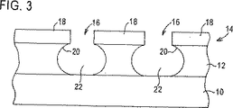
複数の島18を創造するために、シリコン層にトレンチ16をエッチングするステップの次に、埋め込み酸化層12が、アンダーカッティングエッチプロセスでエッチングされる。図3にこのアンダーカッティングエッチの結果が描かれている。従来のエッチング技術が、埋め込み酸化層12をエッチングするために実行され得る。アンダーカット(符号20に示されるような)が埋め込み酸化層12において呈示されているように、穏やかな異方性技術(moderately anisotropic technology)が実行され得る。それ故、実行されたエッチングによって陥凹部即ちリセス部22が、埋め込み酸化層12において創造される。このリセス部22は、シリコン酸化層14におけるトレンチ16の真下の部分とシリコン島18の下の部分を含む。エッチングは、トレンチ16を貫通し、埋め込み酸化層12に進行し、アンダーカット20が埋め込み酸化層12に形成されるまで続けられ得る。等方性プロセスを用いられることが可能であるが、これに代えて、穏やかな異方性プロセスを用いてもよい。アンダーカットする総量を、シリコン島18におけるひずみ量の影響するようコントロールすることもできる。つまり、デポジットされるべき材料を選択することに加えて、埋め込み酸化層12に創造されたリセス部22のサイズは、シリコン島に導入されるひずみに影響を与えることになる。
To create a plurality of
埋め込み酸化層12にリセス部22を、又、複数シリコン島18間にトレンチ16を形成した後に、埋め込み酸化層12からエッチングされた酸化物に置き換えられる新しい材料が導入される。プラズマ気相成長法(PECVD)のような従来のデポジション技術が、リセス部22とトレンチ16において材料24をデポジットするために実行され得る。この材料は、シリコン島18内に導入された実質的なひずみ量に効果を与える材料固有の特性に従って選択される。例えば、トレンチ16によって形成されたリセス部22と間隙部を充填するために窒化物を用いることができる。この固有特性に起因して、図4に示された構造に引張応力が与えられる。圧縮応力のような引張応力の異なる材料や、異なるタイプの応力、例えば圧縮応力を与える材料を選択してもよい。当業者にとって、求められた応力度と応力形式を生じさせるために材料の固有特性に基づき、適切な材料を選択することは可能である。
After forming the
図4に示す構造を形成するために、材料24は、化学的機械研磨(CMP:chemical mechanical polishing)のような従来の平坦化技術によって平坦化される。図4に示す構造における置換材料24によって与えられた応力は、シリコン島18に実質的にひずみ量を導入する。この実質的なひずみ量は、シリコン島18におけるシリコン膜のキャリアの電気的特性を改変する。それ故、次に形成されるSOIデバイスのデバイスパフォーマンスは、改善される。
To form the structure shown in FIG. 4, the
図5は、半導体デバイス26がシリコン島18に形成された後の図4の構造を示す。埋め込み酸化層12、及び複数のシリコン島18の間における代替材料24によって導入された、シリコン島18のひずみシリコンが起因して、デバイス26におけるチャンネル移動度が改善され、デバイスは増加したパーフォーマンスを示す。
FIG. 5 shows the structure of FIG. 4 after the
これらの材料は、実施例のみのためであり、他の材料が本発明の趣旨と範囲内で用いられ得る。 These materials are for illustrative purposes only, and other materials may be used within the spirit and scope of the present invention.
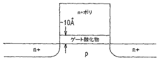
他の形態においては、、ゲート絶縁体の異なる膜厚によってゲート絶縁体のリークを減少するための方法が提供される。ゲート絶縁膜リークは、ドレインとソース領域に最も生じる、チャンネルの真ん中での発生率は4〜5桁程度低くなっている。トンネルは、絶縁体膜厚に指数関数的に依存するので、ゲートリークを抑制するためにソース/ドレインの縁において比較的膜厚を高くすることが求められている。チャンネル反転のゲートのコントロールを増加するために何れの場所においても薄膜絶縁体の需要がある。 In another aspect, a method is provided for reducing gate insulator leakage with different gate insulator thicknesses. The gate insulating film leakage occurs most in the drain and source regions, and the incidence in the middle of the channel is about 4 to 5 digits lower. Since the tunnel depends exponentially on the insulator film thickness, it is required that the film thickness be relatively high at the edge of the source / drain in order to suppress gate leakage. There is a need for thin film insulators everywhere to increase the control of the channel inversion gate.
エクステンションインプラント(extension implants)をアニーリングした後、ゲート酸化物は、フッ化水素緩衝液で側面からエッチングされる。このフッ化水素緩衝液は、エッチングレートコントロールが非常に容易なものである。伸長接合の縁における側面エッチングが実行される。次に、ゲートとシリコンの双方が低温度で酸化される(例えば、ドーパントの拡散の進行を防ぐために750℃より低温でなされる)。ドープされたポリシリコンとn+Siは、軽くドープされたp型チャンネルよりかなり高速で酸化する。 After annealing extension implants, the gate oxide is etched from the side with a hydrogen fluoride buffer. This hydrogen fluoride buffer is very easy to control the etching rate. Side etching at the edges of the stretch bond is performed. Next, both the gate and silicon are oxidized at a low temperature (eg, at a temperature below 750 ° C. to prevent the diffusion of dopants). Doped polysilicon and n + Si oxidize much faster than lightly doped p-type channels.
前述の酸化の後、25〜30オングストロームの膜厚の絶縁体は、n+領域上に形成される。この膜厚は、大きなリークを急激に減少させ、又、ミラーキャパシタンスも減少させる。このプロセスは、次にスペーサ形成、ソース/ドレイン注入、そしてシリサイドと続く。このプロセスは、図6と図7に描かれている。 After the oxidation described above, an insulator with a thickness of 25-30 Angstroms is formed on the n + region. This film thickness drastically reduces large leaks and also reduces mirror capacitance. This process is then followed by spacer formation, source / drain implantation, and silicide. This process is depicted in FIGS. 6 and 7.
本発明は、詳細にわたって記載され、図示されたが、説明目的と例をあげるためのみのものであって、これに制限されるためのものではないことが明瞭に理解されなければならない。本発明の範囲は、添付した請求項の文言によってのみ限定される。 Although the present invention has been described and illustrated in detail, it should be clearly understood that the purpose is illustrative only and not intended to be limiting. The scope of the invention is limited only by the language of the appended claims.
Claims (9)
前記埋め込み酸化層及び前記トレンチの前記リセス部に、前記シリコン層にひずみを導入する材料を充填するステップを有し、
前記リセス部のエッチングは、前記トレンチの真下の部分の前記埋め込み酸化層がエッチングされて前記シリコン島の下のアンダーカット部が形成されるようになされ、前記アンダーカット部のエッチング量は、前記材料により導入されたひずみに影響を与えるようにコントロールされる、
ひずみデバイス膜の形成方法。Etching a recess in a buried oxide layer in a silicon on insulator (SOI) structure comprising a substrate, a buried oxide layer on the substrate, and a silicon layer on the buried oxide layer, the silicon layer having a trench In the etching of the recess portion into the buried oxide layer, the etching is performed so that the silicon layer is etched through the trench and stops at the upper interface on the substrate through the buried oxide layer. Made,
Wherein the recessed portion of the buried oxide layer and the trench, have a step of filling a material to introduce strain into the silicon layer,
The recess portion is etched such that the buried oxide layer immediately below the trench is etched to form an undercut portion under the silicon island, and the etching amount of the undercut portion is determined by the material Controlled to affect the strain introduced by the
Strain device film forming method.
請求項1記載の方法。The step of etching the recess portion (22) includes a process of isotropically etching the buried oxide layer (12).
The method of claim 1.
請求項2記載の方法。The material (24) is a nitride,
The method of claim 2.
前記基板上の埋め込み酸化層(12)を有し、
前記埋め込み酸化層(12)上のシリコン島(18)を有し、このシリコン島(18)は、互いに間隙部(16)によって絶縁され、前記埋め込み酸化層(12)は、前記基板の上方でかつ前記間隙部(16)の直下にリセス部(22)を備え、かつ、前記リセス部(22)は、前記シリコン島(18)の下方に伸長しているアンダーカット領域(20)を含むものであり、
前記リセス部(22)と前記間隙部(16)を充填する材料を含み、前記材料は、前記シリコン島(18)にひずみを導入するものであり、
前記アンダーカット部のエッチング量は、前記材料により導入されたひずみに影響を与えるようにコントロールされる、
ひずみシリコン膜を備えたシリコンオンインシュレータ(SOI)デバイス。Having a substrate (10);
Having a buried oxide layer (12) on the substrate;
There is a silicon island (18) on the buried oxide layer (12), which is insulated from each other by a gap (16), and the buried oxide layer (12) is located above the substrate. A recess portion (22) is provided immediately below the gap portion (16), and the recess portion (22) includes an undercut region (20) extending below the silicon island (18). And
Includes material filling the recess portion (22) of the gap portion (16), said material state, and are not to introduce distortion into the silicon islands (18),
The etching amount of the undercut part is controlled so as to influence the strain introduced by the material,
Silicon-on-insulator (SOI) device with strained silicon film.
請求項7記載のSOIデバイス。In addition, a semiconductor device (26) is included on the silicon island (18).
The SOI device according to claim 7 .
請求項7記載のSOIデバイス。The material (24) is a nitride,
The SOI device according to claim 7 .
Applications Claiming Priority (2)
| Application Number | Priority Date | Filing Date | Title |
|---|---|---|---|
| US10/178,542 US6680240B1 (en) | 2002-06-25 | 2002-06-25 | Silicon-on-insulator device with strained device film and method for making the same with partial replacement of isolation oxide |
| PCT/US2003/017824 WO2004001798A2 (en) | 2002-06-25 | 2003-06-04 | A silicon-on-insulator device with strained device film and method for making the same with partial replacement of isolation oxide |
Publications (3)
| Publication Number | Publication Date |
|---|---|
| JP2005531144A JP2005531144A (en) | 2005-10-13 |
| JP2005531144A5 JP2005531144A5 (en) | 2006-07-20 |
| JP4452883B2 true JP4452883B2 (en) | 2010-04-21 |
Family
ID=29999123
Family Applications (1)
| Application Number | Title | Priority Date | Filing Date |
|---|---|---|---|
| JP2004515743A Expired - Fee Related JP4452883B2 (en) | 2002-06-25 | 2003-06-04 | Silicon-on-insulator device having strained device film partially substituted with insulating oxide and method for manufacturing the same |
Country Status (8)
| Country | Link |
|---|---|
| US (1) | US6680240B1 (en) |
| EP (1) | EP1516362A2 (en) |
| JP (1) | JP4452883B2 (en) |
| KR (1) | KR100996725B1 (en) |
| CN (1) | CN1333454C (en) |
| AU (1) | AU2003238916A1 (en) |
| TW (1) | TWI289895B (en) |
| WO (1) | WO2004001798A2 (en) |
Families Citing this family (73)
| Publication number | Priority date | Publication date | Assignee | Title |
|---|---|---|---|---|
| US6573126B2 (en) * | 2000-08-16 | 2003-06-03 | Massachusetts Institute Of Technology | Process for producing semiconductor article using graded epitaxial growth |
| WO2002082514A1 (en) * | 2001-04-04 | 2002-10-17 | Massachusetts Institute Of Technology | A method for semiconductor device fabrication |
| WO2003079415A2 (en) * | 2002-03-14 | 2003-09-25 | Amberwave Systems Corporation | Methods for fabricating strained layers on semiconductor substrates |
| US6995430B2 (en) * | 2002-06-07 | 2006-02-07 | Amberwave Systems Corporation | Strained-semiconductor-on-insulator device structures |
| US20030227057A1 (en) * | 2002-06-07 | 2003-12-11 | Lochtefeld Anthony J. | Strained-semiconductor-on-insulator device structures |
| US7335545B2 (en) * | 2002-06-07 | 2008-02-26 | Amberwave Systems Corporation | Control of strain in device layers by prevention of relaxation |
| US7074623B2 (en) * | 2002-06-07 | 2006-07-11 | Amberwave Systems Corporation | Methods of forming strained-semiconductor-on-insulator finFET device structures |
| US7307273B2 (en) * | 2002-06-07 | 2007-12-11 | Amberwave Systems Corporation | Control of strain in device layers by selective relaxation |
| US7358121B2 (en) * | 2002-08-23 | 2008-04-15 | Intel Corporation | Tri-gate devices and methods of fabrication |
| US6946373B2 (en) * | 2002-11-20 | 2005-09-20 | International Business Machines Corporation | Relaxed, low-defect SGOI for strained Si CMOS applications |
| FR2847715B1 (en) * | 2002-11-25 | 2005-03-11 | Commissariat Energie Atomique | INTEGRATED CIRCUIT COMPRISING SERIES CONNECTED SUBASSEMBLIES |
| US6717216B1 (en) * | 2002-12-12 | 2004-04-06 | International Business Machines Corporation | SOI based field effect transistor having a compressive film in undercut area under the channel and a method of making the device |
| US7157774B2 (en) * | 2003-01-31 | 2007-01-02 | Taiwan Semiconductor Manufacturing Co., Ltd. | Strained silicon-on-insulator transistors with mesa isolation |
| US6870179B2 (en) * | 2003-03-31 | 2005-03-22 | Intel Corporation | Increasing stress-enhanced drive current in a MOS transistor |
| US7081395B2 (en) * | 2003-05-23 | 2006-07-25 | Taiwan Semiconductor Manufacturing Co., Ltd. | Silicon strain engineering accomplished via use of specific shallow trench isolation fill materials |
| US7456476B2 (en) * | 2003-06-27 | 2008-11-25 | Intel Corporation | Nonplanar semiconductor device with partially or fully wrapped around gate electrode and methods of fabrication |
| US6909151B2 (en) * | 2003-06-27 | 2005-06-21 | Intel Corporation | Nonplanar device with stress incorporation layer and method of fabrication |
| US7105390B2 (en) * | 2003-12-30 | 2006-09-12 | Intel Corporation | Nonplanar transistors with metal gate electrodes |
| US7268058B2 (en) * | 2004-01-16 | 2007-09-11 | Intel Corporation | Tri-gate transistors and methods to fabricate same |
| US20050186722A1 (en) * | 2004-02-25 | 2005-08-25 | Kuan-Lun Cheng | Method and structure for CMOS device with stress relaxed by ion implantation of carbon or oxygen containing ions |
| US7154118B2 (en) * | 2004-03-31 | 2006-12-26 | Intel Corporation | Bulk non-planar transistor having strained enhanced mobility and methods of fabrication |
| US20050266632A1 (en) * | 2004-05-26 | 2005-12-01 | Yun-Hsiu Chen | Integrated circuit with strained and non-strained transistors, and method of forming thereof |
| US7579280B2 (en) * | 2004-06-01 | 2009-08-25 | Intel Corporation | Method of patterning a film |
| US7042009B2 (en) * | 2004-06-30 | 2006-05-09 | Intel Corporation | High mobility tri-gate devices and methods of fabrication |
| US6991998B2 (en) * | 2004-07-02 | 2006-01-31 | International Business Machines Corporation | Ultra-thin, high quality strained silicon-on-insulator formed by elastic strain transfer |
| US7348284B2 (en) * | 2004-08-10 | 2008-03-25 | Intel Corporation | Non-planar pMOS structure with a strained channel region and an integrated strained CMOS flow |
| US7135372B2 (en) * | 2004-09-09 | 2006-11-14 | Taiwan Semiconductor Manufacturing Company, Ltd. | Strained silicon device manufacturing method |
| US7071064B2 (en) * | 2004-09-23 | 2006-07-04 | Intel Corporation | U-gate transistors and methods of fabrication |
| US7332439B2 (en) * | 2004-09-29 | 2008-02-19 | Intel Corporation | Metal gate transistors with epitaxial source and drain regions |
| US7422946B2 (en) * | 2004-09-29 | 2008-09-09 | Intel Corporation | Independently accessed double-gate and tri-gate transistors in same process flow |
| US7361958B2 (en) | 2004-09-30 | 2008-04-22 | Intel Corporation | Nonplanar transistors with metal gate electrodes |
| JP4603845B2 (en) * | 2004-10-12 | 2010-12-22 | Okiセミコンダクタ株式会社 | Manufacturing method of semiconductor device |
| US20060086977A1 (en) * | 2004-10-25 | 2006-04-27 | Uday Shah | Nonplanar device with thinned lower body portion and method of fabrication |
| US7306997B2 (en) * | 2004-11-10 | 2007-12-11 | Advanced Micro Devices, Inc. | Strained fully depleted silicon on insulator semiconductor device and manufacturing method therefor |
| US20060113603A1 (en) * | 2004-12-01 | 2006-06-01 | Amberwave Systems Corporation | Hybrid semiconductor-on-insulator structures and related methods |
| US7393733B2 (en) * | 2004-12-01 | 2008-07-01 | Amberwave Systems Corporation | Methods of forming hybrid fin field-effect transistor structures |
| US7193279B2 (en) * | 2005-01-18 | 2007-03-20 | Intel Corporation | Non-planar MOS structure with a strained channel region |
| US7518196B2 (en) | 2005-02-23 | 2009-04-14 | Intel Corporation | Field effect transistor with narrow bandgap source and drain regions and method of fabrication |
| US20060202266A1 (en) * | 2005-03-14 | 2006-09-14 | Marko Radosavljevic | Field effect transistor with metal source/drain regions |
| US7563701B2 (en) * | 2005-03-31 | 2009-07-21 | Intel Corporation | Self-aligned contacts for transistors |
| US7858481B2 (en) * | 2005-06-15 | 2010-12-28 | Intel Corporation | Method for fabricating transistor with thinned channel |
| US7547637B2 (en) * | 2005-06-21 | 2009-06-16 | Intel Corporation | Methods for patterning a semiconductor film |
| US7279375B2 (en) * | 2005-06-30 | 2007-10-09 | Intel Corporation | Block contact architectures for nanoscale channel transistors |
| US7402875B2 (en) * | 2005-08-17 | 2008-07-22 | Intel Corporation | Lateral undercut of metal gate in SOI device |
| US20070090416A1 (en) * | 2005-09-28 | 2007-04-26 | Doyle Brian S | CMOS devices with a single work function gate electrode and method of fabrication |
| US7479421B2 (en) * | 2005-09-28 | 2009-01-20 | Intel Corporation | Process for integrating planar and non-planar CMOS transistors on a bulk substrate and article made thereby |
| US20070090408A1 (en) * | 2005-09-29 | 2007-04-26 | Amlan Majumdar | Narrow-body multiple-gate FET with dominant body transistor for high performance |
| US7759739B2 (en) * | 2005-10-27 | 2010-07-20 | International Business Machines Corporation | Transistor with dielectric stressor elements |
| DE102005052055B3 (en) | 2005-10-31 | 2007-04-26 | Advanced Micro Devices, Inc., Sunnyvale | Transistor and semiconductor components and production process for thin film silicon on insulator transistor has embedded deformed layer |
| GB2445511B (en) * | 2005-10-31 | 2009-04-08 | Advanced Micro Devices Inc | An embedded strain layer in thin soi transistors and a method of forming the same |
| US7485503B2 (en) | 2005-11-30 | 2009-02-03 | Intel Corporation | Dielectric interface for group III-V semiconductor device |
| US7396711B2 (en) * | 2005-12-27 | 2008-07-08 | Intel Corporation | Method of fabricating a multi-cornered film |
| US7449373B2 (en) * | 2006-03-31 | 2008-11-11 | Intel Corporation | Method of ion implanting for tri-gate devices |
| US7670928B2 (en) * | 2006-06-14 | 2010-03-02 | Intel Corporation | Ultra-thin oxide bonding for S1 to S1 dual orientation bonding |
| US7544594B2 (en) * | 2006-06-28 | 2009-06-09 | Intel Corporation | Method of forming a transistor having gate protection and transistor formed according to the method |
| US8143646B2 (en) | 2006-08-02 | 2012-03-27 | Intel Corporation | Stacking fault and twin blocking barrier for integrating III-V on Si |
| KR100835413B1 (en) * | 2006-12-05 | 2008-06-04 | 동부일렉트로닉스 주식회사 | Method for forming a small via hole of the semiconductor device |
| US20080157225A1 (en) * | 2006-12-29 | 2008-07-03 | Suman Datta | SRAM and logic transistors with variable height multi-gate transistor architecture |
| US8558278B2 (en) * | 2007-01-16 | 2013-10-15 | Taiwan Semiconductor Manufacturing Company, Ltd. | Strained transistor with optimized drive current and method of forming |
| KR101052868B1 (en) * | 2008-02-29 | 2011-07-29 | 주식회사 하이닉스반도체 | SOI element and its manufacturing method |
| US7943961B2 (en) * | 2008-03-13 | 2011-05-17 | Taiwan Semiconductor Manufacturing Company, Ltd. | Strain bars in stressed layers of MOS devices |
| US8362566B2 (en) | 2008-06-23 | 2013-01-29 | Intel Corporation | Stress in trigate devices using complimentary gate fill materials |
| US20100019322A1 (en) * | 2008-07-23 | 2010-01-28 | International Business Machines Corporation | Semiconductor device and method of manufacturing |
| US7808051B2 (en) * | 2008-09-29 | 2010-10-05 | Taiwan Semiconductor Manufacturing Company, Ltd. | Standard cell without OD space effect in Y-direction |
| CN102024706B (en) * | 2009-09-22 | 2012-06-20 | 中芯国际集成电路制造(上海)有限公司 | Method for manufacturing semiconductor device |
| US8258031B2 (en) * | 2010-06-15 | 2012-09-04 | International Business Machines Corporation | Fabrication of a vertical heterojunction tunnel-FET |
| US9406798B2 (en) * | 2010-08-27 | 2016-08-02 | Acorn Technologies, Inc. | Strained semiconductor using elastic edge relaxation of a stressor combined with buried insulating layer |
| JP6005364B2 (en) * | 2012-02-06 | 2016-10-12 | ラピスセミコンダクタ株式会社 | Semiconductor device manufacturing method and semiconductor device |
| US9515181B2 (en) | 2014-08-06 | 2016-12-06 | Qualcomm Incorporated | Semiconductor device with self-aligned back side features |
| JP6559745B2 (en) | 2017-08-23 | 2019-08-14 | 株式会社東芝 | Semiconductor device inspection apparatus, semiconductor device inspection method, program thereof, semiconductor device and manufacturing method thereof |
| JP2018032877A (en) * | 2017-11-29 | 2018-03-01 | ラピスセミコンダクタ株式会社 | Semiconductor device |
| JP2019125747A (en) | 2018-01-18 | 2019-07-25 | 株式会社東芝 | Semiconductor device and method for manufacturing the same |
| KR102396978B1 (en) * | 2018-11-16 | 2022-05-11 | 삼성전자주식회사 | Semiconductor device |
Family Cites Families (23)
| Publication number | Priority date | Publication date | Assignee | Title |
|---|---|---|---|---|
| US4604162A (en) * | 1983-06-13 | 1986-08-05 | Ncr Corporation | Formation and planarization of silicon-on-insulator structures |
| US5270265A (en) * | 1992-09-01 | 1993-12-14 | Harris Corporation | Stress relief technique of removing oxide from surface of trench-patterned semiconductor-on-insulator structure |
| US5561302A (en) | 1994-09-26 | 1996-10-01 | Motorola, Inc. | Enhanced mobility MOSFET device and method |
| US5811283A (en) * | 1996-08-13 | 1998-09-22 | United Microelectronics Corporation | Silicon on insulator (SOI) dram cell structure and process |
| US6211039B1 (en) | 1996-11-12 | 2001-04-03 | Micron Technology, Inc. | Silicon-on-insulator islands and method for their formation |
| US6045625A (en) * | 1996-12-06 | 2000-04-04 | Texas Instruments Incorporated | Buried oxide with a thermal expansion matching layer for SOI |
| GB2327146A (en) * | 1997-07-10 | 1999-01-13 | Ericsson Telefon Ab L M | Thermal insulation of integrated circuit components |
| JP3676910B2 (en) * | 1997-07-30 | 2005-07-27 | インターナショナル・ビジネス・マシーンズ・コーポレーション | Semiconductor device and method for forming semiconductor island |
| US6054343A (en) * | 1998-01-26 | 2000-04-25 | Texas Instruments Incorporated | Nitride trench fill process for increasing shallow trench isolation (STI) robustness |
| JP2000294623A (en) * | 1999-04-02 | 2000-10-20 | Fuji Electric Co Ltd | Manufacture of dielectric separating substrate |
| JP2000332099A (en) * | 1999-05-21 | 2000-11-30 | Matsushita Electronics Industry Corp | Semiconductor device and manufacture thereof |
| US6245600B1 (en) * | 1999-07-01 | 2001-06-12 | International Business Machines Corporation | Method and structure for SOI wafers to avoid electrostatic discharge |
| US6573565B2 (en) * | 1999-07-28 | 2003-06-03 | International Business Machines Corporation | Method and structure for providing improved thermal conduction for silicon semiconductor devices |
| US6426252B1 (en) * | 1999-10-25 | 2002-07-30 | International Business Machines Corporation | Silicon-on-insulator vertical array DRAM cell with self-aligned buried strap |
| US20020046985A1 (en) * | 2000-03-24 | 2002-04-25 | Daneman Michael J. | Process for creating an electrically isolated electrode on a sidewall of a cavity in a base |
| US6403482B1 (en) * | 2000-06-28 | 2002-06-11 | International Business Machines Corporation | Self-aligned junction isolation |
| TW501227B (en) * | 2000-08-11 | 2002-09-01 | Samsung Electronics Co Ltd | SOI MOSFET having body contact for preventing floating body effect and method of fabricating the same |
| DE10040464A1 (en) * | 2000-08-18 | 2002-02-28 | Infineon Technologies Ag | Trench capacitor and process for its manufacture |
| JP2002076336A (en) * | 2000-09-01 | 2002-03-15 | Mitsubishi Electric Corp | Semiconductor device and soi substrate |
| GB0022329D0 (en) * | 2000-09-12 | 2000-10-25 | Mitel Semiconductor Ltd | Semiconductor device |
| DE10054109C2 (en) * | 2000-10-31 | 2003-07-10 | Advanced Micro Devices Inc | Method of forming a substrate contact in a field effect transistor formed over a buried insulating layer |
| US6506620B1 (en) * | 2000-11-27 | 2003-01-14 | Microscan Systems Incorporated | Process for manufacturing micromechanical and microoptomechanical structures with backside metalization |
| US6524929B1 (en) * | 2001-02-26 | 2003-02-25 | Advanced Micro Devices, Inc. | Method for shallow trench isolation using passivation material for trench bottom liner |
-
2002
- 2002-06-25 US US10/178,542 patent/US6680240B1/en not_active Expired - Lifetime
-
2003
- 2003-06-04 KR KR1020047021192A patent/KR100996725B1/en not_active IP Right Cessation
- 2003-06-04 WO PCT/US2003/017824 patent/WO2004001798A2/en active Application Filing
- 2003-06-04 EP EP03734436A patent/EP1516362A2/en not_active Withdrawn
- 2003-06-04 JP JP2004515743A patent/JP4452883B2/en not_active Expired - Fee Related
- 2003-06-04 AU AU2003238916A patent/AU2003238916A1/en not_active Abandoned
- 2003-06-04 CN CNB03813263XA patent/CN1333454C/en not_active Expired - Lifetime
- 2003-06-18 TW TW092116498A patent/TWI289895B/en not_active IP Right Cessation
Also Published As
| Publication number | Publication date |
|---|---|
| TWI289895B (en) | 2007-11-11 |
| EP1516362A2 (en) | 2005-03-23 |
| WO2004001798A3 (en) | 2004-07-29 |
| KR20050013248A (en) | 2005-02-03 |
| US6680240B1 (en) | 2004-01-20 |
| KR100996725B1 (en) | 2010-11-25 |
| AU2003238916A8 (en) | 2004-01-06 |
| TW200400564A (en) | 2004-01-01 |
| CN1333454C (en) | 2007-08-22 |
| JP2005531144A (en) | 2005-10-13 |
| CN1659696A (en) | 2005-08-24 |
| US20040018668A1 (en) | 2004-01-29 |
| AU2003238916A1 (en) | 2004-01-06 |
| WO2004001798A2 (en) | 2003-12-31 |
Similar Documents
| Publication | Publication Date | Title |
|---|---|---|
| JP4452883B2 (en) | Silicon-on-insulator device having strained device film partially substituted with insulating oxide and method for manufacturing the same | |
| US7355262B2 (en) | Diffusion topography engineering for high performance CMOS fabrication | |
| US7442618B2 (en) | Method to engineer etch profiles in Si substrate for advanced semiconductor devices | |
| JP4750342B2 (en) | MOS-FET, manufacturing method thereof, and semiconductor device | |
| US6787423B1 (en) | Strained-silicon semiconductor device | |
| WO2011160477A1 (en) | Strained-channel field-effect transistor and manufacturing method thereof | |
| JP2008041901A (en) | Semiconductor device and its manufacturing method | |
| US20070020828A1 (en) | Method for manufacturing semiconductor apparatus and the semiconductor apparatus | |
| JP2006165480A (en) | Semiconductor device | |
| JP5666451B2 (en) | Structurally strained substrate for forming strained transistors with active layer thickness reduction | |
| US7541258B2 (en) | Method of manufacturing semiconductor substrate and method of manufacturing semiconductor device | |
| KR100374227B1 (en) | Manufacturing method for semiconductor device | |
| KR100886708B1 (en) | Soi device and method for fabricating the same | |
| US20090166813A1 (en) | Method for manufacturing semiconductor device and semiconductor device | |
| JP4619140B2 (en) | MOS field effect transistor and manufacturing method thereof | |
| CN103367226A (en) | Manufacturing method of semiconductor device | |
| US20090170293A1 (en) | Method for manufacturing semiconductor device | |
| KR100344765B1 (en) | Method for isolating semiconductor devices | |
| JPH09223730A (en) | Semiconductor device and manufacturing method thereof | |
| US20130260532A1 (en) | Method for Manufacturing Semiconductor Device | |
| KR100833594B1 (en) | Mosfet device and manufacturing method thereof | |
| JP4943394B2 (en) | Manufacturing method of semiconductor device | |
| KR20060077546A (en) | Method for manufacturing semiconductor device | |
| JP2009152485A (en) | Manufacturing method of semiconductor device, and semiconductor device | |
| TW201415559A (en) | Transistor and fabrication method thereof |
Legal Events
| Date | Code | Title | Description |
|---|---|---|---|
| A521 | Written amendment |
Free format text: JAPANESE INTERMEDIATE CODE: A523 Effective date: 20060605 |
|
| A621 | Written request for application examination |
Free format text: JAPANESE INTERMEDIATE CODE: A621 Effective date: 20060605 |
|
| A977 | Report on retrieval |
Free format text: JAPANESE INTERMEDIATE CODE: A971007 Effective date: 20080708 |
|
| A131 | Notification of reasons for refusal |
Free format text: JAPANESE INTERMEDIATE CODE: A131 Effective date: 20080715 |
|
| A601 | Written request for extension of time |
Free format text: JAPANESE INTERMEDIATE CODE: A601 Effective date: 20081015 |
|
| A602 | Written permission of extension of time |
Free format text: JAPANESE INTERMEDIATE CODE: A602 Effective date: 20081022 |
|
| A601 | Written request for extension of time |
Free format text: JAPANESE INTERMEDIATE CODE: A601 Effective date: 20081117 |
|
| A602 | Written permission of extension of time |
Free format text: JAPANESE INTERMEDIATE CODE: A602 Effective date: 20081125 |
|
| A601 | Written request for extension of time |
Free format text: JAPANESE INTERMEDIATE CODE: A601 Effective date: 20081215 |
|
| A521 | Written amendment |
Free format text: JAPANESE INTERMEDIATE CODE: A523 Effective date: 20081219 |
|
| A602 | Written permission of extension of time |
Free format text: JAPANESE INTERMEDIATE CODE: A602 Effective date: 20081222 |
|
| TRDD | Decision of grant or rejection written | ||
| A01 | Written decision to grant a patent or to grant a registration (utility model) |
Free format text: JAPANESE INTERMEDIATE CODE: A01 Effective date: 20091215 |
|
| A01 | Written decision to grant a patent or to grant a registration (utility model) |
Free format text: JAPANESE INTERMEDIATE CODE: A01 |
|
| A61 | First payment of annual fees (during grant procedure) |
Free format text: JAPANESE INTERMEDIATE CODE: A61 Effective date: 20100114 |
|
| FPAY | Renewal fee payment (event date is renewal date of database) |
Free format text: PAYMENT UNTIL: 20130212 Year of fee payment: 3 |
|
| R150 | Certificate of patent or registration of utility model |
Free format text: JAPANESE INTERMEDIATE CODE: R150 |
|
| LAPS | Cancellation because of no payment of annual fees |