JP4452627B2 - Integrated circuit assembly - Google Patents
Integrated circuit assembly Download PDFInfo
- Publication number
- JP4452627B2 JP4452627B2 JP2004560802A JP2004560802A JP4452627B2 JP 4452627 B2 JP4452627 B2 JP 4452627B2 JP 2004560802 A JP2004560802 A JP 2004560802A JP 2004560802 A JP2004560802 A JP 2004560802A JP 4452627 B2 JP4452627 B2 JP 4452627B2
- Authority
- JP
- Japan
- Prior art keywords
- trace
- integrated circuit
- substrate
- circuit assembly
- die
- Prior art date
- Legal status (The legal status is an assumption and is not a legal conclusion. Google has not performed a legal analysis and makes no representation as to the accuracy of the status listed.)
- Expired - Fee Related
Links
Images


Classifications
-
- H—ELECTRICITY
- H01—ELECTRIC ELEMENTS
- H01L—SEMICONDUCTOR DEVICES NOT COVERED BY CLASS H10
- H01L23/00—Details of semiconductor or other solid state devices
- H01L23/52—Arrangements for conducting electric current within the device in operation from one component to another, i.e. interconnections, e.g. wires, lead frames
- H01L23/538—Arrangements for conducting electric current within the device in operation from one component to another, i.e. interconnections, e.g. wires, lead frames the interconnection structure between a plurality of semiconductor chips being formed on, or in, insulating substrates
-
- H—ELECTRICITY
- H01—ELECTRIC ELEMENTS
- H01L—SEMICONDUCTOR DEVICES NOT COVERED BY CLASS H10
- H01L23/00—Details of semiconductor or other solid state devices
- H01L23/12—Mountings, e.g. non-detachable insulating substrates
- H01L23/13—Mountings, e.g. non-detachable insulating substrates characterised by the shape
-
- H—ELECTRICITY
- H01—ELECTRIC ELEMENTS
- H01L—SEMICONDUCTOR DEVICES NOT COVERED BY CLASS H10
- H01L23/00—Details of semiconductor or other solid state devices
- H01L23/48—Arrangements for conducting electric current to or from the solid state body in operation, e.g. leads, terminal arrangements ; Selection of materials therefor
- H01L23/488—Arrangements for conducting electric current to or from the solid state body in operation, e.g. leads, terminal arrangements ; Selection of materials therefor consisting of soldered or bonded constructions
- H01L23/495—Lead-frames or other flat leads
- H01L23/49503—Lead-frames or other flat leads characterised by the die pad
- H01L23/4951—Chip-on-leads or leads-on-chip techniques, i.e. inner lead fingers being used as die pad
-
- H—ELECTRICITY
- H01—ELECTRIC ELEMENTS
- H01L—SEMICONDUCTOR DEVICES NOT COVERED BY CLASS H10
- H01L23/00—Details of semiconductor or other solid state devices
- H01L23/52—Arrangements for conducting electric current within the device in operation from one component to another, i.e. interconnections, e.g. wires, lead frames
- H01L23/538—Arrangements for conducting electric current within the device in operation from one component to another, i.e. interconnections, e.g. wires, lead frames the interconnection structure between a plurality of semiconductor chips being formed on, or in, insulating substrates
- H01L23/5386—Geometry or layout of the interconnection structure
-
- H—ELECTRICITY
- H01—ELECTRIC ELEMENTS
- H01L—SEMICONDUCTOR DEVICES NOT COVERED BY CLASS H10
- H01L23/00—Details of semiconductor or other solid state devices
- H01L23/52—Arrangements for conducting electric current within the device in operation from one component to another, i.e. interconnections, e.g. wires, lead frames
- H01L23/538—Arrangements for conducting electric current within the device in operation from one component to another, i.e. interconnections, e.g. wires, lead frames the interconnection structure between a plurality of semiconductor chips being formed on, or in, insulating substrates
- H01L23/5387—Flexible insulating substrates
-
- H—ELECTRICITY
- H01—ELECTRIC ELEMENTS
- H01L—SEMICONDUCTOR DEVICES NOT COVERED BY CLASS H10
- H01L24/00—Arrangements for connecting or disconnecting semiconductor or solid-state bodies; Methods or apparatus related thereto
- H01L24/01—Means for bonding being attached to, or being formed on, the surface to be connected, e.g. chip-to-package, die-attach, "first-level" interconnects; Manufacturing methods related thereto
- H01L24/42—Wire connectors; Manufacturing methods related thereto
- H01L24/47—Structure, shape, material or disposition of the wire connectors after the connecting process
- H01L24/49—Structure, shape, material or disposition of the wire connectors after the connecting process of a plurality of wire connectors
-
- H—ELECTRICITY
- H01—ELECTRIC ELEMENTS
- H01L—SEMICONDUCTOR DEVICES NOT COVERED BY CLASS H10
- H01L24/00—Arrangements for connecting or disconnecting semiconductor or solid-state bodies; Methods or apparatus related thereto
- H01L24/01—Means for bonding being attached to, or being formed on, the surface to be connected, e.g. chip-to-package, die-attach, "first-level" interconnects; Manufacturing methods related thereto
- H01L24/50—Tape automated bonding [TAB] connectors, i.e. film carriers; Manufacturing methods related thereto
-
- H—ELECTRICITY
- H01—ELECTRIC ELEMENTS
- H01L—SEMICONDUCTOR DEVICES NOT COVERED BY CLASS H10
- H01L25/00—Assemblies consisting of a plurality of individual semiconductor or other solid state devices ; Multistep manufacturing processes thereof
- H01L25/03—Assemblies consisting of a plurality of individual semiconductor or other solid state devices ; Multistep manufacturing processes thereof all the devices being of a type provided for in the same subgroup of groups H01L27/00 - H01L33/00, or in a single subclass of H10K, H10N, e.g. assemblies of rectifier diodes
- H01L25/04—Assemblies consisting of a plurality of individual semiconductor or other solid state devices ; Multistep manufacturing processes thereof all the devices being of a type provided for in the same subgroup of groups H01L27/00 - H01L33/00, or in a single subclass of H10K, H10N, e.g. assemblies of rectifier diodes the devices not having separate containers
- H01L25/065—Assemblies consisting of a plurality of individual semiconductor or other solid state devices ; Multistep manufacturing processes thereof all the devices being of a type provided for in the same subgroup of groups H01L27/00 - H01L33/00, or in a single subclass of H10K, H10N, e.g. assemblies of rectifier diodes the devices not having separate containers the devices being of a type provided for in group H01L27/00
- H01L25/0655—Assemblies consisting of a plurality of individual semiconductor or other solid state devices ; Multistep manufacturing processes thereof all the devices being of a type provided for in the same subgroup of groups H01L27/00 - H01L33/00, or in a single subclass of H10K, H10N, e.g. assemblies of rectifier diodes the devices not having separate containers the devices being of a type provided for in group H01L27/00 the devices being arranged next to each other
-
- H—ELECTRICITY
- H01—ELECTRIC ELEMENTS
- H01L—SEMICONDUCTOR DEVICES NOT COVERED BY CLASS H10
- H01L2224/00—Indexing scheme for arrangements for connecting or disconnecting semiconductor or solid-state bodies and methods related thereto as covered by H01L24/00
- H01L2224/01—Means for bonding being attached to, or being formed on, the surface to be connected, e.g. chip-to-package, die-attach, "first-level" interconnects; Manufacturing methods related thereto
- H01L2224/02—Bonding areas; Manufacturing methods related thereto
- H01L2224/04—Structure, shape, material or disposition of the bonding areas prior to the connecting process
- H01L2224/0401—Bonding areas specifically adapted for bump connectors, e.g. under bump metallisation [UBM]
-
- H—ELECTRICITY
- H01—ELECTRIC ELEMENTS
- H01L—SEMICONDUCTOR DEVICES NOT COVERED BY CLASS H10
- H01L2224/00—Indexing scheme for arrangements for connecting or disconnecting semiconductor or solid-state bodies and methods related thereto as covered by H01L24/00
- H01L2224/01—Means for bonding being attached to, or being formed on, the surface to be connected, e.g. chip-to-package, die-attach, "first-level" interconnects; Manufacturing methods related thereto
- H01L2224/02—Bonding areas; Manufacturing methods related thereto
- H01L2224/04—Structure, shape, material or disposition of the bonding areas prior to the connecting process
- H01L2224/05—Structure, shape, material or disposition of the bonding areas prior to the connecting process of an individual bonding area
- H01L2224/0554—External layer
- H01L2224/0555—Shape
- H01L2224/05552—Shape in top view
- H01L2224/05554—Shape in top view being square
-
- H—ELECTRICITY
- H01—ELECTRIC ELEMENTS
- H01L—SEMICONDUCTOR DEVICES NOT COVERED BY CLASS H10
- H01L2224/00—Indexing scheme for arrangements for connecting or disconnecting semiconductor or solid-state bodies and methods related thereto as covered by H01L24/00
- H01L2224/01—Means for bonding being attached to, or being formed on, the surface to be connected, e.g. chip-to-package, die-attach, "first-level" interconnects; Manufacturing methods related thereto
- H01L2224/02—Bonding areas; Manufacturing methods related thereto
- H01L2224/04—Structure, shape, material or disposition of the bonding areas prior to the connecting process
- H01L2224/06—Structure, shape, material or disposition of the bonding areas prior to the connecting process of a plurality of bonding areas
- H01L2224/061—Disposition
- H01L2224/0612—Layout
- H01L2224/0613—Square or rectangular array
- H01L2224/06134—Square or rectangular array covering only portions of the surface to be connected
- H01L2224/06136—Covering only the central area of the surface to be connected, i.e. central arrangements
-
- H—ELECTRICITY
- H01—ELECTRIC ELEMENTS
- H01L—SEMICONDUCTOR DEVICES NOT COVERED BY CLASS H10
- H01L2224/00—Indexing scheme for arrangements for connecting or disconnecting semiconductor or solid-state bodies and methods related thereto as covered by H01L24/00
- H01L2224/01—Means for bonding being attached to, or being formed on, the surface to be connected, e.g. chip-to-package, die-attach, "first-level" interconnects; Manufacturing methods related thereto
- H01L2224/10—Bump connectors; Manufacturing methods related thereto
- H01L2224/15—Structure, shape, material or disposition of the bump connectors after the connecting process
- H01L2224/16—Structure, shape, material or disposition of the bump connectors after the connecting process of an individual bump connector
- H01L2224/161—Disposition
- H01L2224/16151—Disposition the bump connector connecting between a semiconductor or solid-state body and an item not being a semiconductor or solid-state body, e.g. chip-to-substrate, chip-to-passive
- H01L2224/16221—Disposition the bump connector connecting between a semiconductor or solid-state body and an item not being a semiconductor or solid-state body, e.g. chip-to-substrate, chip-to-passive the body and the item being stacked
- H01L2224/16225—Disposition the bump connector connecting between a semiconductor or solid-state body and an item not being a semiconductor or solid-state body, e.g. chip-to-substrate, chip-to-passive the body and the item being stacked the item being non-metallic, e.g. insulating substrate with or without metallisation
-
- H—ELECTRICITY
- H01—ELECTRIC ELEMENTS
- H01L—SEMICONDUCTOR DEVICES NOT COVERED BY CLASS H10
- H01L2224/00—Indexing scheme for arrangements for connecting or disconnecting semiconductor or solid-state bodies and methods related thereto as covered by H01L24/00
- H01L2224/01—Means for bonding being attached to, or being formed on, the surface to be connected, e.g. chip-to-package, die-attach, "first-level" interconnects; Manufacturing methods related thereto
- H01L2224/26—Layer connectors, e.g. plate connectors, solder or adhesive layers; Manufacturing methods related thereto
- H01L2224/31—Structure, shape, material or disposition of the layer connectors after the connecting process
- H01L2224/32—Structure, shape, material or disposition of the layer connectors after the connecting process of an individual layer connector
- H01L2224/321—Disposition
- H01L2224/32151—Disposition the layer connector connecting between a semiconductor or solid-state body and an item not being a semiconductor or solid-state body, e.g. chip-to-substrate, chip-to-passive
- H01L2224/32221—Disposition the layer connector connecting between a semiconductor or solid-state body and an item not being a semiconductor or solid-state body, e.g. chip-to-substrate, chip-to-passive the body and the item being stacked
- H01L2224/32225—Disposition the layer connector connecting between a semiconductor or solid-state body and an item not being a semiconductor or solid-state body, e.g. chip-to-substrate, chip-to-passive the body and the item being stacked the item being non-metallic, e.g. insulating substrate with or without metallisation
-
- H—ELECTRICITY
- H01—ELECTRIC ELEMENTS
- H01L—SEMICONDUCTOR DEVICES NOT COVERED BY CLASS H10
- H01L2224/00—Indexing scheme for arrangements for connecting or disconnecting semiconductor or solid-state bodies and methods related thereto as covered by H01L24/00
- H01L2224/01—Means for bonding being attached to, or being formed on, the surface to be connected, e.g. chip-to-package, die-attach, "first-level" interconnects; Manufacturing methods related thereto
- H01L2224/42—Wire connectors; Manufacturing methods related thereto
- H01L2224/47—Structure, shape, material or disposition of the wire connectors after the connecting process
- H01L2224/48—Structure, shape, material or disposition of the wire connectors after the connecting process of an individual wire connector
- H01L2224/4805—Shape
- H01L2224/4809—Loop shape
- H01L2224/48091—Arched
-
- H—ELECTRICITY
- H01—ELECTRIC ELEMENTS
- H01L—SEMICONDUCTOR DEVICES NOT COVERED BY CLASS H10
- H01L2224/00—Indexing scheme for arrangements for connecting or disconnecting semiconductor or solid-state bodies and methods related thereto as covered by H01L24/00
- H01L2224/01—Means for bonding being attached to, or being formed on, the surface to be connected, e.g. chip-to-package, die-attach, "first-level" interconnects; Manufacturing methods related thereto
- H01L2224/42—Wire connectors; Manufacturing methods related thereto
- H01L2224/47—Structure, shape, material or disposition of the wire connectors after the connecting process
- H01L2224/48—Structure, shape, material or disposition of the wire connectors after the connecting process of an individual wire connector
- H01L2224/481—Disposition
- H01L2224/48135—Connecting between different semiconductor or solid-state bodies, i.e. chip-to-chip
- H01L2224/48137—Connecting between different semiconductor or solid-state bodies, i.e. chip-to-chip the bodies being arranged next to each other, e.g. on a common substrate
- H01L2224/48139—Connecting between different semiconductor or solid-state bodies, i.e. chip-to-chip the bodies being arranged next to each other, e.g. on a common substrate with an intermediate bond, e.g. continuous wire daisy chain
-
- H—ELECTRICITY
- H01—ELECTRIC ELEMENTS
- H01L—SEMICONDUCTOR DEVICES NOT COVERED BY CLASS H10
- H01L2224/00—Indexing scheme for arrangements for connecting or disconnecting semiconductor or solid-state bodies and methods related thereto as covered by H01L24/00
- H01L2224/01—Means for bonding being attached to, or being formed on, the surface to be connected, e.g. chip-to-package, die-attach, "first-level" interconnects; Manufacturing methods related thereto
- H01L2224/42—Wire connectors; Manufacturing methods related thereto
- H01L2224/47—Structure, shape, material or disposition of the wire connectors after the connecting process
- H01L2224/48—Structure, shape, material or disposition of the wire connectors after the connecting process of an individual wire connector
- H01L2224/481—Disposition
- H01L2224/48151—Connecting between a semiconductor or solid-state body and an item not being a semiconductor or solid-state body, e.g. chip-to-substrate, chip-to-passive
- H01L2224/48221—Connecting between a semiconductor or solid-state body and an item not being a semiconductor or solid-state body, e.g. chip-to-substrate, chip-to-passive the body and the item being stacked
- H01L2224/48225—Connecting between a semiconductor or solid-state body and an item not being a semiconductor or solid-state body, e.g. chip-to-substrate, chip-to-passive the body and the item being stacked the item being non-metallic, e.g. insulating substrate with or without metallisation
- H01L2224/4824—Connecting between the body and an opposite side of the item with respect to the body
-
- H—ELECTRICITY
- H01—ELECTRIC ELEMENTS
- H01L—SEMICONDUCTOR DEVICES NOT COVERED BY CLASS H10
- H01L2224/00—Indexing scheme for arrangements for connecting or disconnecting semiconductor or solid-state bodies and methods related thereto as covered by H01L24/00
- H01L2224/01—Means for bonding being attached to, or being formed on, the surface to be connected, e.g. chip-to-package, die-attach, "first-level" interconnects; Manufacturing methods related thereto
- H01L2224/42—Wire connectors; Manufacturing methods related thereto
- H01L2224/47—Structure, shape, material or disposition of the wire connectors after the connecting process
- H01L2224/49—Structure, shape, material or disposition of the wire connectors after the connecting process of a plurality of wire connectors
-
- H—ELECTRICITY
- H01—ELECTRIC ELEMENTS
- H01L—SEMICONDUCTOR DEVICES NOT COVERED BY CLASS H10
- H01L2224/00—Indexing scheme for arrangements for connecting or disconnecting semiconductor or solid-state bodies and methods related thereto as covered by H01L24/00
- H01L2224/73—Means for bonding being of different types provided for in two or more of groups H01L2224/10, H01L2224/18, H01L2224/26, H01L2224/34, H01L2224/42, H01L2224/50, H01L2224/63, H01L2224/71
- H01L2224/732—Location after the connecting process
- H01L2224/73201—Location after the connecting process on the same surface
- H01L2224/73215—Layer and wire connectors
-
- H—ELECTRICITY
- H01—ELECTRIC ELEMENTS
- H01L—SEMICONDUCTOR DEVICES NOT COVERED BY CLASS H10
- H01L24/00—Arrangements for connecting or disconnecting semiconductor or solid-state bodies; Methods or apparatus related thereto
- H01L24/01—Means for bonding being attached to, or being formed on, the surface to be connected, e.g. chip-to-package, die-attach, "first-level" interconnects; Manufacturing methods related thereto
- H01L24/42—Wire connectors; Manufacturing methods related thereto
- H01L24/47—Structure, shape, material or disposition of the wire connectors after the connecting process
- H01L24/48—Structure, shape, material or disposition of the wire connectors after the connecting process of an individual wire connector
-
- H—ELECTRICITY
- H01—ELECTRIC ELEMENTS
- H01L—SEMICONDUCTOR DEVICES NOT COVERED BY CLASS H10
- H01L24/00—Arrangements for connecting or disconnecting semiconductor or solid-state bodies; Methods or apparatus related thereto
- H01L24/80—Methods for connecting semiconductor or other solid state bodies using means for bonding being attached to, or being formed on, the surface to be connected
- H01L24/86—Methods for connecting semiconductor or other solid state bodies using means for bonding being attached to, or being formed on, the surface to be connected using tape automated bonding [TAB]
-
- H—ELECTRICITY
- H01—ELECTRIC ELEMENTS
- H01L—SEMICONDUCTOR DEVICES NOT COVERED BY CLASS H10
- H01L2924/00—Indexing scheme for arrangements or methods for connecting or disconnecting semiconductor or solid-state bodies as covered by H01L24/00
- H01L2924/0001—Technical content checked by a classifier
- H01L2924/00014—Technical content checked by a classifier the subject-matter covered by the group, the symbol of which is combined with the symbol of this group, being disclosed without further technical details
-
- H—ELECTRICITY
- H01—ELECTRIC ELEMENTS
- H01L—SEMICONDUCTOR DEVICES NOT COVERED BY CLASS H10
- H01L2924/00—Indexing scheme for arrangements or methods for connecting or disconnecting semiconductor or solid-state bodies as covered by H01L24/00
- H01L2924/01—Chemical elements
- H01L2924/01004—Beryllium [Be]
-
- H—ELECTRICITY
- H01—ELECTRIC ELEMENTS
- H01L—SEMICONDUCTOR DEVICES NOT COVERED BY CLASS H10
- H01L2924/00—Indexing scheme for arrangements or methods for connecting or disconnecting semiconductor or solid-state bodies as covered by H01L24/00
- H01L2924/01—Chemical elements
- H01L2924/01006—Carbon [C]
-
- H—ELECTRICITY
- H01—ELECTRIC ELEMENTS
- H01L—SEMICONDUCTOR DEVICES NOT COVERED BY CLASS H10
- H01L2924/00—Indexing scheme for arrangements or methods for connecting or disconnecting semiconductor or solid-state bodies as covered by H01L24/00
- H01L2924/01—Chemical elements
- H01L2924/01014—Silicon [Si]
-
- H—ELECTRICITY
- H01—ELECTRIC ELEMENTS
- H01L—SEMICONDUCTOR DEVICES NOT COVERED BY CLASS H10
- H01L2924/00—Indexing scheme for arrangements or methods for connecting or disconnecting semiconductor or solid-state bodies as covered by H01L24/00
- H01L2924/01—Chemical elements
- H01L2924/01015—Phosphorus [P]
-
- H—ELECTRICITY
- H01—ELECTRIC ELEMENTS
- H01L—SEMICONDUCTOR DEVICES NOT COVERED BY CLASS H10
- H01L2924/00—Indexing scheme for arrangements or methods for connecting or disconnecting semiconductor or solid-state bodies as covered by H01L24/00
- H01L2924/01—Chemical elements
- H01L2924/0105—Tin [Sn]
-
- H—ELECTRICITY
- H01—ELECTRIC ELEMENTS
- H01L—SEMICONDUCTOR DEVICES NOT COVERED BY CLASS H10
- H01L2924/00—Indexing scheme for arrangements or methods for connecting or disconnecting semiconductor or solid-state bodies as covered by H01L24/00
- H01L2924/013—Alloys
- H01L2924/014—Solder alloys
-
- H—ELECTRICITY
- H01—ELECTRIC ELEMENTS
- H01L—SEMICONDUCTOR DEVICES NOT COVERED BY CLASS H10
- H01L2924/00—Indexing scheme for arrangements or methods for connecting or disconnecting semiconductor or solid-state bodies as covered by H01L24/00
- H01L2924/10—Details of semiconductor or other solid state devices to be connected
- H01L2924/1015—Shape
- H01L2924/1016—Shape being a cuboid
- H01L2924/10161—Shape being a cuboid with a rectangular active surface
-
- H—ELECTRICITY
- H01—ELECTRIC ELEMENTS
- H01L—SEMICONDUCTOR DEVICES NOT COVERED BY CLASS H10
- H01L2924/00—Indexing scheme for arrangements or methods for connecting or disconnecting semiconductor or solid-state bodies as covered by H01L24/00
- H01L2924/10—Details of semiconductor or other solid state devices to be connected
- H01L2924/11—Device type
- H01L2924/14—Integrated circuits
-
- H—ELECTRICITY
- H01—ELECTRIC ELEMENTS
- H01L—SEMICONDUCTOR DEVICES NOT COVERED BY CLASS H10
- H01L2924/00—Indexing scheme for arrangements or methods for connecting or disconnecting semiconductor or solid-state bodies as covered by H01L24/00
- H01L2924/15—Details of package parts other than the semiconductor or other solid state devices to be connected
- H01L2924/151—Die mounting substrate
- H01L2924/1517—Multilayer substrate
- H01L2924/15192—Resurf arrangement of the internal vias
-
- H—ELECTRICITY
- H01—ELECTRIC ELEMENTS
- H01L—SEMICONDUCTOR DEVICES NOT COVERED BY CLASS H10
- H01L2924/00—Indexing scheme for arrangements or methods for connecting or disconnecting semiconductor or solid-state bodies as covered by H01L24/00
- H01L2924/15—Details of package parts other than the semiconductor or other solid state devices to be connected
- H01L2924/181—Encapsulation
-
- H—ELECTRICITY
- H01—ELECTRIC ELEMENTS
- H01L—SEMICONDUCTOR DEVICES NOT COVERED BY CLASS H10
- H01L2924/00—Indexing scheme for arrangements or methods for connecting or disconnecting semiconductor or solid-state bodies as covered by H01L24/00
- H01L2924/19—Details of hybrid assemblies other than the semiconductor or other solid state devices to be connected
- H01L2924/1901—Structure
- H01L2924/1904—Component type
- H01L2924/19043—Component type being a resistor
-
- H—ELECTRICITY
- H01—ELECTRIC ELEMENTS
- H01L—SEMICONDUCTOR DEVICES NOT COVERED BY CLASS H10
- H01L2924/00—Indexing scheme for arrangements or methods for connecting or disconnecting semiconductor or solid-state bodies as covered by H01L24/00
- H01L2924/19—Details of hybrid assemblies other than the semiconductor or other solid state devices to be connected
- H01L2924/191—Disposition
- H01L2924/19101—Disposition of discrete passive components
- H01L2924/19107—Disposition of discrete passive components off-chip wires
-
- H—ELECTRICITY
- H01—ELECTRIC ELEMENTS
- H01L—SEMICONDUCTOR DEVICES NOT COVERED BY CLASS H10
- H01L2924/00—Indexing scheme for arrangements or methods for connecting or disconnecting semiconductor or solid-state bodies as covered by H01L24/00
- H01L2924/30—Technical effects
- H01L2924/301—Electrical effects
- H01L2924/3011—Impedance
-
- H—ELECTRICITY
- H01—ELECTRIC ELEMENTS
- H01L—SEMICONDUCTOR DEVICES NOT COVERED BY CLASS H10
- H01L2924/00—Indexing scheme for arrangements or methods for connecting or disconnecting semiconductor or solid-state bodies as covered by H01L24/00
- H01L2924/30—Technical effects
- H01L2924/301—Electrical effects
- H01L2924/3025—Electromagnetic shielding
Description
本発明は集積回路に関し、詳しくは基板上にKnow−Good−Dieを使用した集積回路アセンブリに関する。 The present invention relates to an integrated circuit, and more particularly to an integrated circuit assembly using Know-Good-Die on a substrate.
集積回路は、LOC(Lead-Over-Chip)リードフレームに機械的に取り付けられ、且つLOCリードフレームに電気的に接続された半導体ダイを有する場合がある。半導体ダイとリードフレームは通常、プラスチックパッケージ、セラミックパッケージ、または金属パッケージの中にトランスファー封入成形される。パッケージ化されたダイの代わりにKnow−Good−Die(KGD)を使用することにより、製造効率を向上させコストを低減できることがある。KGDとは、検査および/または稼動試験により、他の同等のパッケージ化されたダイと同じ品質および信頼性を有していると概ね判断されたパッケージ化されていないダイのことである。 An integrated circuit may have a semiconductor die that is mechanically attached to a LOC (Lead-Over-Chip) lead frame and electrically connected to the LOC lead frame. The semiconductor die and lead frame are typically transfer encapsulated in a plastic package, ceramic package, or metal package. Using a Know-Good-Die (KGD) instead of a packaged die may improve manufacturing efficiency and reduce costs. A KGD is an unpackaged die that has been generally determined by inspection and / or operational testing to have the same quality and reliability as other equivalent packaged dies.
性能を向上させ、製造コストを低減した集積回路アセンブリと、その製造方法が必要とされている。 What is needed is an integrated circuit assembly with improved performance and reduced manufacturing costs, and a method of manufacturing the same.
大まかに言えば、基板上にKnow−Good−Die(KGD)を使用した改良型集積回路アセンブリを提供する。基板上のパッドをトレースその他の導体に配線要素を用いて電気接続したり、基板上のパッドを他のダイ上のパッドに接続したりする。 Broadly speaking, an improved integrated circuit assembly using Know-Good-Die (KGD) on a substrate is provided. Pads on the substrate are electrically connected to traces or other conductors using wiring elements, or pads on the substrate are connected to pads on other dies.
次に、本発明の原理の理解を助けるために、図面に描かれた実施形態を参照して、具体的な言葉を用いてそれらの実施形態について説明する。ただし、それらに本発明の範囲を制限する意図はなく、例示する装置の変形や変更、並びに本明細書に記載する発明の原理のさらなる応用はすべて、本発明に関連する技術分野の当業者にとって普通に想起されるものと考えられる。 Next, in order to help understanding of the principle of the present invention, specific embodiments will be described with reference to the embodiments illustrated in the drawings. However, they are not intended to limit the scope of the present invention, and variations and modifications of the illustrated apparatus, as well as further applications of the principles of the invention described herein, are all known to those of ordinary skill in the art related to the present invention. It is thought to be recalled normally.
図1および図2は、本発明の一実施形態による集積回路アセンブリ10を示す。アセンブリ10は一般に、複数のダイ、好ましくは事前にテストされたKnow−Good−Die(KGD)12〜15、および複数のボンディングワイヤ18のような配線を含む。基板19は、ダイの組み付けに適したものであればどのような基板でもよく、プリント回路基板、セラミック、プラスチック、可撓性回路などが挙げられるが、それらに限定される訳ではない。全ての集積回路を基板上に組み付ける最終組立ての前または後に、基板19を研削または研磨して基板19を薄くする場合があることに注意して欲しい。トレース21は様々な組み合わせにより、電力、グラウンド、並びにデータ、アドレス、および制御などの信号を基板19に接続された1以上のKGDに提供するためのバスを形成する。基板19には複数の開口部23〜26が互いに間隔を空けて形成され、それらが複数の位置でトレース19を遮断している。開口部のサイズや形は様々であってよく、開口部は基板で完全に囲まれたものでも部分的に囲まれたものでもよく、それらの周辺付近に画定されるものであってもよい。このように、トレース21のうちのあるものは、図示のように隣り合う一組の開口部23〜26間に延び、中央トレース27と呼ばれる。各グループのトレース(すなわち、開口部24と開口部25の間に延びる5本のトレースからなるグループや、開口部23から外側へ向けて延びる5本のトレースからなるグループ)は並んで延び、実質的に平行で、且つ実質的に同じ長さであることが望ましい。場合によっては、縁部補強材28が基板19の十分な部分に結合または使用され、その部分が補強される。図1の実施形態の場合、縁部補強材28は、図示のように基板19の周辺を取り囲む一対の金属ストリップ(1つは上、1つは下)からなる。トレース21のうちのあるものは、基板19の縁部から外側へ向けて延び、上位回路に接続するためのコネクタ29を形成する。基板19の縁部から外側へ向けて延びるトレースは、縁部トレース30と呼ばれる。縁部トレース30は補強材28を貫通して延びている。補強材28は、ヒートシンクとして機能するサイズおよび構成にしてもよい。ヒートシンクのサイズ、形、組成はどのようなものでもよく、棒状、プレート状、周囲フレーム(全部または一部)、その他が挙げられるが、それらに限定される訳ではない。基板19が薄いものである場合(例えば、可撓性回路材料のような可撓性フィルムの場合)、補強材28は、通常ならばダイの重さで湾曲してしまうであろう可撓性フィルム基板を実質的に平坦な形状に保つのに役立つ。ただし、上記のように可撓性フィルムは基板の一例に過ぎない。もっと硬い基板を使用すれば(例えば、プリント回路基板材料など)、補強材は不要な場合もある。
1 and 2 illustrate an
米国特許第6,214,641B1号および第6,219,908B1号に記載されているように(これらは参照によって取り込まれる)、Know−Good−Die(KGD)とは、検査および/または稼動試験により、他の同等のパッケージ化されたダイと同じ品質および信頼性を概ね有しているものと判断されたパッケージ化されていないダイのことである。こうしたKGDは基板に固定され、コンピュータ、電気通信装置、自動車、腕時計、電気器具、そして恐らくは非常に様々な電子機器に使用されるマルチチップモジュールを形成する。図1の集積回路アセンブリにおいて、KGD12〜15はそれぞれ1以上の電気的なダイ接点、すなわちダイパッド31を有している。各ダイパッド31は、KGDの電気接点(例えば、グラウンド接続、電力接続、信号接続などに使用される)として機能する。ダイパッドの形や数は、ダイの設計に応じて任意の適当な形および数であってよい。KGD12〜15は(図2に示すように)基板19の下面32に固定され、ダイパッド31は対応する開口部23〜26の中に配置される。すなわち、ダイパッド31には、基板19の上面から開口部を通じて接続することができる。KGD12〜15を基板19に固定する手段は、接着剤33のような一般的な任意の適当な手段であってよい。一般的なボンディング技術を使用して、トレース21からダイパッド31までワイヤ18を接続したり、あるトレースの一端36から別のトレースの一端37まで開口部24をまたいでワイヤ18をジャンパ接続したりすることができる。ワイヤ接続を容易にするために、トレース端部(例えば36や37)は開口部23〜26の近くにおいてそれぞれ拡大されているので、ワイヤはそのようなトレース端部に接続することが望ましい。ただし、必要に応じて、あるいは特定の電気的構成を実現するために、トレース上の任意の点に1以上のワイヤ18を接続する場合もあるものと考えられる。
As described in US Pat. Nos. 6,214,641B1 and 6,219,908B1, which are incorporated by reference, Know-Good-Die (KGD) is an inspection and / or operational test. Thus, an unpackaged die that has been determined to generally have the same quality and reliability as other equivalent packaged dies. These KGDs are secured to a substrate and form a multichip module used in computers, telecommunications devices, automobiles, watches, appliances, and possibly a great variety of electronic equipment. In the integrated circuit assembly of FIG. 1, each of the KGDs 12-15 has one or more electrical die contacts or die
図3は、基板19の下側のダイ面にだけ補強材39(およびヒートシンク)を使用する代替実施形態を示している。この例の場合、基板19は可撓性回路であり、可撓性回路は外縁34まで延び、そこで捲り返されるか、または小さな挿入基板(図示せず)を巻き込んで捲り返され、上位回路に接続するための代替接続面を形成する。
FIG. 3 shows an alternative embodiment that uses reinforcement 39 (and a heat sink) only on the lower die surface of
図4および図5は、代替実施形態による集積回路アセンブリ40を示す。トレース21からなる層とトレース41からなる層の2つの層が、基板19に取り付けられている。トレース41の通り道は絶縁層42に埋め込まれ、トレース21とトレース41の間が絶縁層42により絶縁されている。トレース21からなる上側の層は図1の実施形態と同様に長手方向に延び、トレース41からなる下側の層はそのトレース21に対して横向きに、すなわち概ね垂直に延びている。トレース41の外側の端部は基板19および補強材44から外向きに延び、基板19の一部に沿ってその上にコネクタ43が形成される。バイア46は基板19を貫通して延び、長手方向に延びる上側トレース21を、それを横切る方向に延びる下側トレース41に接続する働きをする。このような長手方向に延びるトレース、横切る方向に延びるトレース、およびバイアは、複雑な多層回路構造を形成するために、基板19のどの部分に形成してもよい。例えば、基板19の開口部23〜26の上および/または下にある層に途切れのないトレースを設け、別の層にその長手方向に延びるトレースから開口部間の表面領域まで通じる垂直バイアを形成し、さらに、バイアからダイパッドまでワイヤを接続する場合がある。横切る方向のトレースは、長手方向のトレース21に対して概ね垂直に延びるものとして描かれている。ただし、この第2の下側トレース41は、上側のトレース21に対して90度以外の角度で、互いに平行にならない角度で配置される場合もある。第2のトレース層(もし有れば第3のトレース層や第4のトレース層も)は単に、上側トレースの層に対して相互排他的であればよい。
4 and 5 show an
図6〜図8は、基板48が多層化された代替実施形態による集積回路アセンブリ47を示す。バストレース49(図7に描かれ、図6にも1本だけ破線で描かれている)はトレース21と同様に基板48に埋め込まれ、開口部50〜53により分断されている。開口部50〜53のうちの1つに向かって延びる大部分のトレース49の端部は、接合端55を形成する。基板48の上側を外側へ向けて延びるトレース49は、その一端46に上位回路と接続するためのコネクタ57を形成する。集積回路アセンブリ10と同様に、接合端55から基板48の裏面に取り付けられたKGD60〜63のダイパッド58にワイヤ64を接続したり、ある接合端55から別の接合端55にワイヤ64を接続したりすることができる。アセンブリ47は更に、グラウンド平面トレース64と電源平面トレース67を有し、これらがそれぞれ基板48の上側を長手方向に延びている。グラウンドトレース66と電源トレース67は、バイアにより基板48に接続され(グラウンドトレース66の場合、符号69で示されているように)、それぞれ対応する横方向のトレース49に接続され、横方向の埋め込みグラウンドトレースと横方向の埋め込み電源トレースを形成している(図面にはグラウンドトレース70しか描いていない)。基板48から外向きに延びるグラウンドトレースおよび電源トレースは、基板48の縁部56に、上位回路と接続するためのグランドコネクタ72および電源コネクタ73を形成している。
6-8 illustrate an integrated circuit assembly 47 according to an alternative embodiment in which the
信号反射を抑制または低減するために、任意選択で、バスの末端部またはその近くに(任意形状の)抵抗器を設けてもよい。抵抗器は、ボンディングワイヤその他の配線要素によりトレースに接続される。任意選択で、抵抗器はグラウンドに接続してもよい。また、トレース間、またはトレースの周りにワイヤ、トレース、シールド、フィルムなどを配置し、アセンブリのトレース間または他の導体間における電気信号その他の信号の干渉を抑制または防止してもよい。 Optionally, a resistor (of any shape) may be provided at or near the end of the bus to suppress or reduce signal reflection. The resistor is connected to the trace by a bonding wire or other wiring element. Optionally, the resistor may be connected to ground. Also, wires, traces, shields, films, etc. may be placed between or around the traces to suppress or prevent electrical or other signal interference between the traces of the assembly or other conductors.
グラウンド平面トレース66と電源平面トレース67を基板48へ向けて下向きに折り曲げ(符号69に示すように)た後、さらに外向きに折り曲げ、基板48の縁部56から取り出してグラウンドコネクタ72と電源コネクタ73を直接形成し、グラウンドトレース70や電源トレース71を使用しない代替実施形態も考えられる。
The
グラウンドや電源をグラウンドトレース70と電源トレース71のみによって供給し、グランドトレース70と電源トレース71を縁部コネクタ71および72で終端し、グラウンド平面トレース66や電源平面トレース67を全く形成しない代替実施形態も考えられる。
An alternative embodiment in which ground or power is supplied by
グラウンド平面トレース66と電源平面トレース67をバストレース(図1のトレース21のような)で置き換える実施形態も考えられ、その場合、埋め込みグラウンドトレース70および/または埋め込み電源トレース71は使用してもしなくてもよい。
Embodiments in which the
バストレースを基板48の外側表面に設け(図1や他の図面のトレース21のように)、そこに接続されたボンディングワイヤを用いて、必要に応じて電源、グラウンド、信号などを供給する代替実施形態も考えられる。このような表面実装型バストレースは、本明細書に記載する埋め込みトレースや平面トレースの代わりに設けてもよいし、それらに追加して設けてもよい。
An alternative to providing bus traces on the outer surface of the substrate 48 (like
図9は、KGD77〜80が基板81の両面に取り付けられた代替実施形態による集積回路アセンブリ76を示す。 FIG. 9 shows an integrated circuit assembly 76 according to an alternative embodiment with KGD 77-80 attached to both sides of the substrate 81. FIG.
図10は、図1や図2のアセンブリ10と同様にバストレース83が基板84に表面実装された代替実施形態による集積回路アセンブリ82を示す。KGD86〜89は基板84の両面に表面実装され、少なくとも1つのKGDが表面実装トレース83の上に直接取り付けられている。KGD87および89をトレース83上に取り付けできるようにするために、一部のトレース83は図示のように対応する開口部91および92の中にまで延び、そこにワイヤ93を接続できるようになっている。あるいは、図4および図5の集積回路アセンブリ40について説明したように、複数階層のトレースを使用してもよい。例えば、基板開口部の上および/または下にある層に途切れのない横方向トレースを設け、別の層にそれらの横方向トレースから開口部間の領域まで延びる垂直トレースを設け、さらに、垂直トレースからダイパッドまでワイヤを接続することもできる。このようなトレース構成は、基板の片面に設けることも両面に設けることもできる。
FIG. 10 shows an integrated circuit assembly 82 according to an alternative embodiment in which a
図11は、複数の縁部トレース96が外側の開口部から外側へ向けて延び、基板長手方向の中間点まで折り返し、基板の横縁から外側へ延びて横縁コネクタ97を形成する、代替実施形態による集積回路アセンブリ95を示す。
FIG. 11 shows an alternative implementation in which a plurality of edge traces 96 extend outwardly from the outer opening, fold back to the mid-board midpoint, and extend outwardly from the lateral edge of the substrate to form the
図1〜図11に開示した実施形態の種々の態様を詳しく開示されていない組み合わせで組み合わせた実施形態も考えられる。限定はしないが例えば、図11の実施形態は、基板の上面と下面の両方に取り付けられたKGDを有することもでき、および/または、2以上の異なるトレース層を有することもできる。種々の形の補強材、カバー、および/または、他の適当な保護材料(参照により本明細書に取り込まれた米国特許第6,214,641号に開示されている非導電性粘性物質の塊など)を基板、および/または、基板の周りに使用し、基板、KGD、トレース、ワイヤなどを補強または保護する実施形態も考えられる。KGD、ワイヤおよび関連部品を支持するとともに、取り扱い、およびいかなる磨耗および亀裂にも耐える何らかの適当な材料から基板を構成する実施形態も考えられる。限定はしないが、そうした材料には、可撓性のシリコン、セラミック、エポキシ樹脂、ポリアミド、テフロン、フッ素樹脂の他、有機材料や誘電体材料などがある。 Embodiments combining various aspects of the embodiments disclosed in FIGS. 1-11 in combinations not disclosed in detail are also contemplated. For example, without limitation, the embodiment of FIG. 11 can have a KGD attached to both the top and bottom surfaces of the substrate, and / or can have two or more different trace layers. Various forms of reinforcements, covers, and / or other suitable protective materials (a mass of non-conductive viscous material as disclosed in US Pat. No. 6,214,641, incorporated herein by reference) Etc.) may be used to reinforce or protect the substrate, KGD, traces, wires, etc. using the substrate and / or around the substrate. Embodiments are also contemplated in which the substrate is constructed from any suitable material that supports the KGD, wires, and related components, and that is resistant to handling and any wear and cracking. Such materials include, but are not limited to, flexible silicon, ceramics, epoxy resins, polyamides, Teflon, fluororesins, organic materials and dielectric materials.
図12および図13は、トレース106がバスとして機能するように配線された集積回路アセンブリ105の一構成例を示す。つまり、バスの形成は、各トレースの端部(例えば107)をワイヤ109でダイパッド108に接続した後、さらにそれを次のトレース端部(例えば110)に別のワイヤ109で接続することにより行われる。
12 and 13 show an example configuration of the
図14は、集積回路アセンブリ105と同様にトレースがバスとして機能するように配線された代替実施形態による集積回路アセンブリ113を示す。隣りあう各対の開口部(例えば114と115)の間において、基板117の上に配置されたトレース116は、バイア118により基板117下側のトレース119に接続される。KGDは、フィルム117の上側と下側に交互に取り付けられ、あるKGDのダイパッド120は、図示のようにワイヤ121、上側トレース116、下側トレース119、およびもう1つのワイヤ121を介して隣りのKGD124のダイパッド120に接続される。このようにして、すべてのKGD123〜126が実質的に共通バスに沿って接続される。あるいは、バイア118で相互接続された互い違い構成のトレース(すなわち116と119)を何らかの所望の態様でKGDに接続し、それを連続バス等にしてもよい。図7のグラウンドトレース70のように、基板19の上面と下面の間にグラウンド平面板を埋め込む代替実施形態も考えられる。こうしたグラウンド平面板は、バイアおよびトレースのインピーダンスを調節するのに使用される。グラウンド平面板は、任意の所望の形に作成することができる。グラウンド平面版は、例えば図6のトレース49と同じくらい細く作成してもよいし、基板の全幅と同じくらい太く作成することもでき、両者の間の任意の幅または形に作成することができる。グラウンド平面板は、絶縁された開口部を有することが望ましく、その中に1以上のバイア118を通すことが望ましい。トレースのうちの1以上は、グラウンド平面板に接続される場合がある。
FIG. 14 shows an
図15は、図5の集積回路アセンブリ40に似た代替実施形態による集積回路アセンブリ132を示す。ただし、横方向に延びるトレース134が基板19に埋め込まれ、トレース134が必要に応じてバイア136により上側の長手方向に延びるトレース135の層に接続されている点が異なる。
FIG. 15 shows an
本明細書に記載する実施形態は、トレースをダイパッドや他のトレースに接続するための配線としてワイヤ(例えば、図1のワイヤ18)を使用している。本発明で使用される配線には、ある電気的なダイ接点またはトレースを別の電気的なダイ接点またはトレースに電気接続するのに適した任意のデバイス、材料または要素が含まれる。他の配線や、他の配線を使用する方法も考えられ、限定はしないが、例えば導電性ポリマー、接着剤またはエポキシなどをリソグラフィにより転写し、マスクスクリーンやディスペンサを使用するといった方法もある。図16〜図17はさらに他の実施形態を示す。図16に示す集積回路アセンブリ139では、超音波ボンディングにより、あるトレース141から別のトレース142までストリップトレース140を接着している。図17の場合、ストリップトレース140は、あるトレース141からダイパッド143まで下がり、反対側の隣りのトレース142に戻るように接着される。
The embodiments described herein use wires (eg,
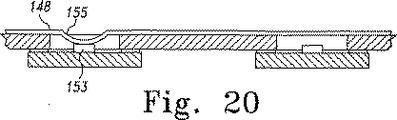
図18〜図19は、ストリップトレース148が基板149の長手方向に沿って種々の開口部151および152の上に配置された代替回路アセンブリ147を示す。その後必要に応じて、ワイヤボンディングや本明細書に記載している他の方法などの任意の適当な方法を用いて、ストリップトレース148がその下のダイパッド153に接続される。ストリップトレース148をダイパッド158に接続する方法は他にもあり、例えば導電性ボール154(図19)を使用すること、ストリップトレース148を接着するときにバンプ155を最初から形成しておくこと(図20)、ストリップトレース148を接着(図18のように)した後でストリップトレース148のダイパッドの位置を変形させ、接続用バンプ155を形成することなどが考えられる。あるいは、トレースを接続しようとするダイパッド153の上に、バンプやボールを直接形成してもよい(ダイを基板に接着する前に行うのが好ましい)。
FIGS. 18-19 illustrate
図21は、図17の構造を示し、トレース141と配線要素140の上に第1の絶縁材料160が配置されている。第1の絶縁材料160の上に導電体層162が配置され、導電体層162の上に第2の絶縁材料164が配置される。トレース141および配線要素140のインピーダンスを調節するために、導電体層162はグラウンドまたは電源に接続することができる。あるいは、導電体層162は、グラウンドにも電源にも接続せず、トレース141、配線要素140およびダイ123を単にシールドするものにしてもよい。当然ながら、層160、162および164は、アセンブリの一部を包むものであってもよいし、全体を包むものであってもよい。さらに他の代替として、導電体層162は、基板117に取り付けられた金属ケースであってもよい。そのような場合、層164は空気として実施することができ、層160も空気にすることができる。当然ながら、類似の層160、162、および164は、本明細書に記載しているどの実施形態にも使用することができる。
FIG. 21 shows the structure of FIG. 17, in which a first insulating
図22および図23は、マイクロプロセッサ202がはんだボール218によりトレース210および212に接続される実施形態を示す。4つのメモリダイ204が、図22および図23に示すように、配線要素214およびトレース210によってマイクロプロセッサ202に接続されている。当然ながら、図22および図23は、様々なタイプのダイを組み合わせて電子システムを形成するシステムの一例を示しているに過ぎない。無線周波数ダイ、アナログダイ、ロジックダイ、または、他のタイプのダイを組み合わせて配線することにより、そのようなシステムが形成される。
22 and 23 illustrate an embodiment in which the
図24および図25は、ダイ304が基板306の表面に接着される実施形態を示す。トレース310が、接続端320からダイ304の横の空間まで延びている。配線要素314は、ダイ304上の端子316をトレース310に接続している。また、幾つかの配線要素320は、ダイ304上の端子316を別のダイ上の端子316に接続している。
FIGS. 24 and 25 illustrate an embodiment in which the
図26および図27は、基板406の裏面(すなわち、ダイ404が接着される面)の開口部間にトレース410が配置される、更に他の実施形態を示す。図26および図27に示すように、配線要素414はダイ404上の端子416をバイア420に接続している。バイア420は基板406を貫通してトレース410まで通じている。
FIGS. 26 and 27 show yet another embodiment in which traces 410 are disposed between openings in the back surface of substrate 406 (ie, the surface to which die 404 is bonded). As shown in FIGS. 26 and 27, the
本発明は図面と上記の説明に詳しく描かれ説明されているが、それらは例と考えるべきものであり、制限的性質を有するものではなく、好ましい実施形態を図示説明したものにすぎない。本発明の思想の範囲内に属する変形や変更は、すべて保護されることが望ましい。「a」、「an」、「said」、および「the」という冠詞は、単数の要素に限定するためのものではなく、そのような要素を1以上含むことを意味している。 While the invention has been illustrated and described in detail in the drawings and foregoing description, they are to be considered as illustrative and not restrictive in nature and are merely illustrative of preferred embodiments. It is desirable that all modifications and changes belonging to the scope of the idea of the present invention be protected. The articles “a”, “an”, “said”, and “the” are not intended to be limiting to a single element, but are meant to include one or more such elements.
Claims (17)
前記基板を貫通する第1の開口部と、
前記基板に取り付けられた第1のダイであって、前記開口部の中に位置する第1のダイ接点を有する第1のダイと、
前記基板に取り付けられた第1のトレースと、
前記基板に取り付けられた第2のトレースと、
前記第1の開口部の上をまたいで前記第1のトレースを前記第2のトレースに接続する第1の配線と、
を含む集積回路アセンブリ。A substrate,
A first opening penetrating the substrate;
A first die attached to the substrate, the first die having a first die contact located in the opening;
A first trace attached to the substrate;
A second trace attached to the substrate;
A first interconnect connecting the first trace to the second trace across the first opening;
An integrated circuit assembly.
前記第1のトレースおよび前記第1のダイ接点に接続された第1のワイヤと、
前記第2のトレースおよび前記第1のダイ接点に接続された第2のワイヤと、
を含む、請求項1に記載の集積回路アセンブリ。The first wiring is
A first wire connected to the first trace and the first die contact;
A second wire connected to the second trace and the first die contact;
The integrated circuit assembly of claim 1, comprising:
前記基板に取り付けられた第2のダイであって、前記第2の開口部の中に位置する第2のダイ接点を有する第2のダイと、
前記第2のダイ接点を前記第2のトレースに接続する第2の配線と、
を更に含む、請求項1に記載の集積回路アセンブリ。The substrate further comprises a second opening, and the integrated circuit assembly comprises:
A second die attached to the substrate, the second die having a second die contact located in the second opening;
A second wiring connecting the second die contact to the second trace;
The integrated circuit assembly of claim 1, further comprising:
Applications Claiming Priority (2)
| Application Number | Priority Date | Filing Date | Title |
|---|---|---|---|
| US10/317,661 US7550842B2 (en) | 2002-12-12 | 2002-12-12 | Integrated circuit assembly |
| PCT/US2003/039537 WO2004055895A1 (en) | 2002-12-12 | 2003-12-12 | Integrated circuit assembly |
Publications (3)
| Publication Number | Publication Date |
|---|---|
| JP2006510224A JP2006510224A (en) | 2006-03-23 |
| JP2006510224A5 JP2006510224A5 (en) | 2009-11-05 |
| JP4452627B2 true JP4452627B2 (en) | 2010-04-21 |
Family
ID=32506187
Family Applications (1)
| Application Number | Title | Priority Date | Filing Date |
|---|---|---|---|
| JP2004560802A Expired - Fee Related JP4452627B2 (en) | 2002-12-12 | 2003-12-12 | Integrated circuit assembly |
Country Status (8)
| Country | Link |
|---|---|
| US (1) | US7550842B2 (en) |
| EP (1) | EP1573815A1 (en) |
| JP (1) | JP4452627B2 (en) |
| KR (1) | KR101062260B1 (en) |
| CN (1) | CN100530640C (en) |
| AU (1) | AU2003299608A1 (en) |
| TW (1) | TWI339435B (en) |
| WO (1) | WO2004055895A1 (en) |
Families Citing this family (52)
| Publication number | Priority date | Publication date | Assignee | Title |
|---|---|---|---|---|
| EP1506568B1 (en) * | 2002-04-29 | 2016-06-01 | Samsung Electronics Co., Ltd. | Direct-connect signaling system |
| US7750446B2 (en) | 2002-04-29 | 2010-07-06 | Interconnect Portfolio Llc | IC package structures having separate circuit interconnection structures and assemblies constructed thereof |
| US8324725B2 (en) * | 2004-09-27 | 2012-12-04 | Formfactor, Inc. | Stacked die module |
| US7663216B2 (en) * | 2005-11-02 | 2010-02-16 | Sandisk Corporation | High density three dimensional semiconductor die package |
| US20070241441A1 (en) * | 2006-04-17 | 2007-10-18 | Stats Chippac Ltd. | Multichip package system |
| US7569421B2 (en) * | 2007-05-04 | 2009-08-04 | Stats Chippac, Ltd. | Through-hole via on saw streets |
| US7723157B2 (en) * | 2007-12-28 | 2010-05-25 | Walton Advanced Engineering, Inc. | Method for cutting and molding in small windows to fabricate semiconductor packages |
| TWI370714B (en) * | 2008-01-09 | 2012-08-11 | Ind Tech Res Inst | Circuit structure and menufacturing method thereof |
| US7643305B2 (en) * | 2008-03-07 | 2010-01-05 | Qualcomm Mems Technologies, Inc. | System and method of preventing damage to metal traces of flexible printed circuits |
| JP2010287733A (en) * | 2009-06-11 | 2010-12-24 | Elpida Memory Inc | Semiconductor device |
| KR20110082643A (en) * | 2010-01-12 | 2011-07-20 | 삼성전자주식회사 | Wiring substrate for a semiconductor chip and semiconductor package having the wiring substrate |
| JP2011155203A (en) * | 2010-01-28 | 2011-08-11 | Elpida Memory Inc | Semiconductor device |
| US8786083B2 (en) * | 2010-09-16 | 2014-07-22 | Tessera, Inc. | Impedance controlled packages with metal sheet or 2-layer RDL |
| US9136197B2 (en) | 2010-09-16 | 2015-09-15 | Tessera, Inc. | Impedence controlled packages with metal sheet or 2-layer RDL |
| US9153530B2 (en) * | 2011-06-16 | 2015-10-06 | Broadcom Corporation | Thermal enhanced high density flip chip package |
| US8823165B2 (en) | 2011-07-12 | 2014-09-02 | Invensas Corporation | Memory module in a package |
| US8502390B2 (en) | 2011-07-12 | 2013-08-06 | Tessera, Inc. | De-skewed multi-die packages |
| US8513817B2 (en) | 2011-07-12 | 2013-08-20 | Invensas Corporation | Memory module in a package |
| EP2769409A1 (en) | 2011-10-03 | 2014-08-27 | Invensas Corporation | Stub minimization for multi-die wirebond assemblies with orthogonal windows |
| US8436477B2 (en) | 2011-10-03 | 2013-05-07 | Invensas Corporation | Stub minimization using duplicate sets of signal terminals in assemblies without wirebonds to package substrate |
| US8653646B2 (en) | 2011-10-03 | 2014-02-18 | Invensas Corporation | Stub minimization using duplicate sets of terminals for wirebond assemblies without windows |
| US8610260B2 (en) | 2011-10-03 | 2013-12-17 | Invensas Corporation | Stub minimization for assemblies without wirebonds to package substrate |
| US8441111B2 (en) * | 2011-10-03 | 2013-05-14 | Invensas Corporation | Stub minimization for multi-die wirebond assemblies with parallel windows |
| US8436457B2 (en) * | 2011-10-03 | 2013-05-07 | Invensas Corporation | Stub minimization for multi-die wirebond assemblies with parallel windows |
| JP5887414B2 (en) | 2011-10-03 | 2016-03-16 | インヴェンサス・コーポレイション | Stub minimization of multi-die wirebond assemblies with parallel windows |
| WO2013052544A1 (en) | 2011-10-03 | 2013-04-11 | Invensas Corporation | Stub minimization with terminal grids offset from center of package |
| US8659142B2 (en) | 2011-10-03 | 2014-02-25 | Invensas Corporation | Stub minimization for wirebond assemblies without windows |
| TWI528500B (en) | 2012-03-20 | 2016-04-01 | 鈺創科技股份有限公司 | Bundled memory and manufacture method for a bundled memory with an external input/output bus |
| US9368477B2 (en) | 2012-08-27 | 2016-06-14 | Invensas Corporation | Co-support circuit panel and microelectronic packages |
| US8848392B2 (en) | 2012-08-27 | 2014-09-30 | Invensas Corporation | Co-support module and microelectronic assembly |
| US8787034B2 (en) | 2012-08-27 | 2014-07-22 | Invensas Corporation | Co-support system and microelectronic assembly |
| US8848391B2 (en) | 2012-08-27 | 2014-09-30 | Invensas Corporation | Co-support component and microelectronic assembly |
| US9019710B2 (en) | 2012-10-11 | 2015-04-28 | Apple Inc. | Devices having flexible printed circuits with bent stiffeners |
| US9601557B2 (en) | 2012-11-16 | 2017-03-21 | Apple Inc. | Flexible display |
| US20140191403A1 (en) * | 2013-01-07 | 2014-07-10 | Lsi Corporation | Multi-die semiconductor package and method of manufacturing thereof |
| US9070423B2 (en) | 2013-06-11 | 2015-06-30 | Invensas Corporation | Single package dual channel memory with co-support |
| KR101416159B1 (en) * | 2013-09-06 | 2014-07-14 | 주식회사 기가레인 | Printed curcuit board comprising contact pad |
| US9123555B2 (en) | 2013-10-25 | 2015-09-01 | Invensas Corporation | Co-support for XFD packaging |
| US9281296B2 (en) | 2014-07-31 | 2016-03-08 | Invensas Corporation | Die stacking techniques in BGA memory package for small footprint CPU and memory motherboard design |
| US10153238B2 (en) * | 2014-08-20 | 2018-12-11 | Samsung Display Co., Ltd. | Electrical channel including pattern voids |
| US9691437B2 (en) | 2014-09-25 | 2017-06-27 | Invensas Corporation | Compact microelectronic assembly having reduced spacing between controller and memory packages |
| US9600112B2 (en) * | 2014-10-10 | 2017-03-21 | Apple Inc. | Signal trace patterns for flexible substrates |
| US10154583B1 (en) | 2015-03-27 | 2018-12-11 | Flex Ltd | Mechanical strain reduction on flexible and rigid-flexible circuits |
| US9484080B1 (en) | 2015-11-09 | 2016-11-01 | Invensas Corporation | High-bandwidth memory application with controlled impedance loading |
| US9992880B2 (en) | 2015-11-12 | 2018-06-05 | Multek Technologies Limited | Rigid-bend printed circuit board fabrication |
| US9679613B1 (en) | 2016-05-06 | 2017-06-13 | Invensas Corporation | TFD I/O partition for high-speed, high-density applications |
| US9747934B1 (en) * | 2016-09-13 | 2017-08-29 | Seagate Technology Llc | Flexible dynamic loop with back-side impedance control structures |
| KR20180075733A (en) | 2016-12-26 | 2018-07-05 | 엘지디스플레이 주식회사 | Flexible display device |
| TWI652983B (en) | 2018-04-16 | 2019-03-01 | 緯創資通股份有限公司 | Electronic device and electromagnetic shielding device |
| KR102620865B1 (en) * | 2018-12-03 | 2024-01-04 | 에스케이하이닉스 주식회사 | Semiconductor package |
| KR102538705B1 (en) * | 2018-12-04 | 2023-06-01 | 에스케이하이닉스 주식회사 | Semiconductor package |
| US20230108475A1 (en) * | 2021-10-04 | 2023-04-06 | Formfactor, Inc. | Thermal management techniques for high power integrated circuits operating in dry cryogenic environments |
Family Cites Families (45)
| Publication number | Priority date | Publication date | Assignee | Title |
|---|---|---|---|---|
| US5423497A (en) * | 1965-12-03 | 1995-06-13 | Shorts Missile Systems Limited | Control systems for moving bodies |
| DE3911711A1 (en) * | 1989-04-10 | 1990-10-11 | Ibm | MODULE STRUCTURE WITH INTEGRATED SEMICONDUCTOR CHIP AND CHIP CARRIER |
| GB8918482D0 (en) | 1989-08-14 | 1989-09-20 | Inmos Ltd | Packaging semiconductor chips |
| US5227338A (en) * | 1990-04-30 | 1993-07-13 | International Business Machines Corporation | Three-dimensional memory card structure with internal direct chip attachment |
| US5241456A (en) * | 1990-07-02 | 1993-08-31 | General Electric Company | Compact high density interconnect structure |
| US6219908B1 (en) * | 1991-06-04 | 2001-04-24 | Micron Technology, Inc. | Method and apparatus for manufacturing known good semiconductor die |
| US5243497A (en) | 1992-09-29 | 1993-09-07 | Texas Instruments | Chip on board assembly |
| JPH06151685A (en) * | 1992-11-04 | 1994-05-31 | Mitsubishi Electric Corp | Mcp semiconductor device |
| US5602421A (en) * | 1995-01-31 | 1997-02-11 | Hughes Aircraft Company | Microwave monolithic integrated circuit package with improved RF ports |
| KR0177395B1 (en) * | 1995-04-27 | 1999-05-15 | 문정환 | Chip mounted circuit board and method for manufacturing the same |
| KR0144164B1 (en) * | 1995-05-12 | 1998-07-01 | 문정환 | How to package ELC semiconductor package and semiconductor device |
| US5818698A (en) * | 1995-10-12 | 1998-10-06 | Micron Technology, Inc. | Method and apparatus for a chip-on-board semiconductor module |
| US6667560B2 (en) * | 1996-05-29 | 2003-12-23 | Texas Instruments Incorporated | Board on chip ball grid array |
| US5723907A (en) * | 1996-06-25 | 1998-03-03 | Micron Technology, Inc. | Loc simm |
| US5811879A (en) * | 1996-06-26 | 1998-09-22 | Micron Technology, Inc. | Stacked leads-over-chip multi-chip module |
| US6017776A (en) * | 1997-04-29 | 2000-01-25 | Micron Technology, Inc. | Method of attaching a leadframe to singulated semiconductor dice |
| US5899705A (en) * | 1997-11-20 | 1999-05-04 | Akram; Salman | Stacked leads-over chip multi-chip module |
| US5998860A (en) * | 1997-12-19 | 1999-12-07 | Texas Instruments Incorporated | Double sided single inline memory module |
| US6049129A (en) * | 1997-12-19 | 2000-04-11 | Texas Instruments Incorporated | Chip size integrated circuit package |
| US6249052B1 (en) * | 1998-06-01 | 2001-06-19 | Paul T. Lin | Substrate on chip (SOC) multiple-chip module (MCM) with chip-size-package (CSP) ready configuration |
| TW368707B (en) * | 1998-10-27 | 1999-09-01 | Tech Field Co Ltd | Packaging method for semiconductor die and the product of the same |
| US6455354B1 (en) * | 1998-12-30 | 2002-09-24 | Micron Technology, Inc. | Method of fabricating tape attachment chip-on-board assemblies |
| US6351028B1 (en) * | 1999-02-08 | 2002-02-26 | Micron Technology, Inc. | Multiple die stack apparatus employing T-shaped interposer elements |
| US6856013B1 (en) * | 1999-02-19 | 2005-02-15 | Micron Technology, Inc. | Integrated circuit packages, ball-grid array integrated circuit packages and methods of packaging an integrated circuit |
| JP2000315776A (en) | 1999-05-06 | 2000-11-14 | Hitachi Ltd | Semiconductor device |
| US6387732B1 (en) * | 1999-06-18 | 2002-05-14 | Micron Technology, Inc. | Methods of attaching a semiconductor chip to a leadframe with a footprint of about the same size as the chip and packages formed thereby |
| US6825550B2 (en) * | 1999-09-02 | 2004-11-30 | Micron Technology, Inc. | Board-on-chip packages with conductive foil on the chip surface |
| US6534861B1 (en) * | 1999-11-15 | 2003-03-18 | Substrate Technologies Incorporated | Ball grid substrate for lead-on-chip semiconductor package |
| KR20010064907A (en) * | 1999-12-20 | 2001-07-11 | 마이클 디. 오브라이언 | wire bonding method and semiconductor package using it |
| US6404660B1 (en) * | 1999-12-23 | 2002-06-11 | Rambus, Inc. | Semiconductor package with a controlled impedance bus and method of forming same |
| JP2001223324A (en) * | 2000-02-10 | 2001-08-17 | Mitsubishi Electric Corp | Semiconductor device |
| JP2001274323A (en) * | 2000-03-24 | 2001-10-05 | Hitachi Ltd | Semiconductor device and semiconductor module mounted therewith, and method of manufacturing the same |
| US6522018B1 (en) * | 2000-05-16 | 2003-02-18 | Micron Technology, Inc. | Ball grid array chip packages having improved testing and stacking characteristics |
| US6683377B1 (en) * | 2000-05-30 | 2004-01-27 | Amkor Technology, Inc. | Multi-stacked memory package |
| KR100608608B1 (en) * | 2000-06-23 | 2006-08-09 | 삼성전자주식회사 | Semiconductor chip package having bonding pad structure of mixing type and manufacturing method thereof |
| JP2002074985A (en) * | 2000-08-29 | 2002-03-15 | Mitsubishi Electric Corp | Memory module, its manufacturing method, and test connector using it |
| US20020043709A1 (en) * | 2000-10-13 | 2002-04-18 | Yeh Nai Hua | Stackable integrated circuit |
| JP3652598B2 (en) * | 2000-11-22 | 2005-05-25 | 本田技研工業株式会社 | Internal combustion engine |
| US6680212B2 (en) * | 2000-12-22 | 2004-01-20 | Lucent Technologies Inc | Method of testing and constructing monolithic multi-chip modules |
| US6680213B2 (en) * | 2001-04-02 | 2004-01-20 | Micron Technology, Inc. | Method and system for fabricating contacts on semiconductor components |
| US6706624B1 (en) * | 2001-10-31 | 2004-03-16 | Lockheed Martin Corporation | Method for making multichip module substrates by encapsulating electrical conductors |
| US6835592B2 (en) * | 2002-05-24 | 2004-12-28 | Micron Technology, Inc. | Methods for molding a semiconductor die package with enhanced thermal conductivity |
| US6987031B2 (en) * | 2002-08-27 | 2006-01-17 | Micron Technology, Inc. | Multiple chip semiconductor package and method of fabricating same |
| US7323772B2 (en) * | 2002-08-28 | 2008-01-29 | Micron Technology, Inc. | Ball grid array structures and tape-based method of manufacturing same |
| US6879030B2 (en) * | 2002-09-30 | 2005-04-12 | Ultratera Corporation | Strengthened window-type semiconductor package |
-
2002
- 2002-12-12 US US10/317,661 patent/US7550842B2/en not_active Expired - Fee Related
-
2003
- 2003-12-12 KR KR1020057010632A patent/KR101062260B1/en not_active IP Right Cessation
- 2003-12-12 EP EP03799897A patent/EP1573815A1/en not_active Withdrawn
- 2003-12-12 WO PCT/US2003/039537 patent/WO2004055895A1/en active Application Filing
- 2003-12-12 AU AU2003299608A patent/AU2003299608A1/en not_active Abandoned
- 2003-12-12 CN CNB2003801092161A patent/CN100530640C/en not_active Expired - Fee Related
- 2003-12-12 TW TW92135250A patent/TWI339435B/en not_active IP Right Cessation
- 2003-12-12 JP JP2004560802A patent/JP4452627B2/en not_active Expired - Fee Related
Also Published As
| Publication number | Publication date |
|---|---|
| KR101062260B1 (en) | 2011-09-06 |
| KR20050085561A (en) | 2005-08-29 |
| CN100530640C (en) | 2009-08-19 |
| TWI339435B (en) | 2011-03-21 |
| AU2003299608A1 (en) | 2004-07-09 |
| US20040113250A1 (en) | 2004-06-17 |
| CN1742372A (en) | 2006-03-01 |
| WO2004055895A1 (en) | 2004-07-01 |
| US7550842B2 (en) | 2009-06-23 |
| EP1573815A1 (en) | 2005-09-14 |
| JP2006510224A (en) | 2006-03-23 |
| TW200425462A (en) | 2004-11-16 |
Similar Documents
| Publication | Publication Date | Title |
|---|---|---|
| JP4452627B2 (en) | Integrated circuit assembly | |
| US7508061B2 (en) | Three-dimensional semiconductor module having multi-sided ground block | |
| US6501157B1 (en) | Substrate for accepting wire bonded or flip-chip components | |
| US7372131B2 (en) | Routing element for use in semiconductor device assemblies | |
| US20040217471A1 (en) | Component and assemblies with ends offset downwardly | |
| US20090170240A1 (en) | Optimized Circuit Design Layout for High Performance Ball Grid Array Packages | |
| JPS5860562A (en) | Package for high terminal number integrated circuit device | |
| US20070152310A1 (en) | Electrical ground method for ball stack package | |
| JPH05211275A (en) | Semiconductor device and manufacture thereof | |
| US8791501B1 (en) | Integrated passive device structure and method | |
| JP2011155203A (en) | Semiconductor device | |
| US20090091019A1 (en) | Memory Packages Having Stair Step Interconnection Layers | |
| CN108257945A (en) | Semiconductor devices | |
| US5986886A (en) | Three-dimensional flexible electronic module | |
| US20060278962A1 (en) | Microelectronic loop packages | |
| US6563208B2 (en) | Semiconductor package with conductor impedance selected during assembly | |
| JP2004289156A (en) | Recessed bonded semiconductor package substrate | |
| EP3182449A1 (en) | Semiconductor package | |
| JP5839503B2 (en) | Semiconductor device, LSI (Large Scale Integration) and electronic device | |
| US7772045B1 (en) | Wire bond method for angularly disposed conductive pads and a device made from the method | |
| US7768117B2 (en) | Microelectronic package having interconnected redistribution paths | |
| JP2007248322A (en) | Probe card | |
| WO1999013509A1 (en) | Semiconductor device | |
| JP2010056121A (en) | Multilayer semiconductor device | |
| US20080157320A1 (en) | Laterally Interconnected IC Packages and Methods |
Legal Events
| Date | Code | Title | Description |
|---|---|---|---|
| A621 | Written request for application examination |
Free format text: JAPANESE INTERMEDIATE CODE: A621 Effective date: 20061211 |
|
| RD03 | Notification of appointment of power of attorney |
Free format text: JAPANESE INTERMEDIATE CODE: A7423 Effective date: 20061211 |
|
| A977 | Report on retrieval |
Free format text: JAPANESE INTERMEDIATE CODE: A971007 Effective date: 20090610 |
|
| A131 | Notification of reasons for refusal |
Free format text: JAPANESE INTERMEDIATE CODE: A131 Effective date: 20090612 |
|
| A524 | Written submission of copy of amendment under article 19 pct |
Free format text: JAPANESE INTERMEDIATE CODE: A524 Effective date: 20090914 |
|
| TRDD | Decision of grant or rejection written | ||
| A01 | Written decision to grant a patent or to grant a registration (utility model) |
Free format text: JAPANESE INTERMEDIATE CODE: A01 Effective date: 20100104 |
|
| A01 | Written decision to grant a patent or to grant a registration (utility model) |
Free format text: JAPANESE INTERMEDIATE CODE: A01 |
|
| A61 | First payment of annual fees (during grant procedure) |
Free format text: JAPANESE INTERMEDIATE CODE: A61 Effective date: 20100201 |
|
| R150 | Certificate of patent or registration of utility model |
Free format text: JAPANESE INTERMEDIATE CODE: R150 |
|
| FPAY | Renewal fee payment (event date is renewal date of database) |
Free format text: PAYMENT UNTIL: 20130205 Year of fee payment: 3 |
|
| FPAY | Renewal fee payment (event date is renewal date of database) |
Free format text: PAYMENT UNTIL: 20140205 Year of fee payment: 4 |
|
| LAPS | Cancellation because of no payment of annual fees |