JP4442167B2 - Filter device - Google Patents
Filter device Download PDFInfo
- Publication number
- JP4442167B2 JP4442167B2 JP2003316248A JP2003316248A JP4442167B2 JP 4442167 B2 JP4442167 B2 JP 4442167B2 JP 2003316248 A JP2003316248 A JP 2003316248A JP 2003316248 A JP2003316248 A JP 2003316248A JP 4442167 B2 JP4442167 B2 JP 4442167B2
- Authority
- JP
- Japan
- Prior art keywords
- vibrator
- group
- transducer
- filter device
- frequency
- Prior art date
- Legal status (The legal status is an assumption and is not a legal conclusion. Google has not performed a legal analysis and makes no representation as to the accuracy of the status listed.)
- Expired - Fee Related
Links
Images


Description
本発明は、いわゆるマイクロマシン(超小型電気的・機械的複合体;Micro Electro-Mechanical Systems、以下「MEMS」という)を用いてなるフィルタ装置に関するものである。 The present invention relates to a filter device using a so-called micromachine (micro electro-mechanical system; hereinafter referred to as “MEMS”).
近年、基板上の微細化製造技術の進展に伴い、MEMSやMEMSを組み込んだ小型機器等が注目されている。MEMSは、可動構造体である振動子と、その振動子の駆動を制御する半導体集積回路等とを、電気的・機械的に結合させた素子である。そして、振動子が素子の一部に組み込まれており、その振動子の駆動を電極間のクーロン引力等を応用して電気的に行うようになっている。 In recent years, attention has been paid to MEMS, small devices incorporating MEMS, and the like with the progress of miniaturization manufacturing technology on a substrate. The MEMS is an element obtained by electrically and mechanically coupling a vibrator that is a movable structure and a semiconductor integrated circuit that controls driving of the vibrator. A vibrator is incorporated in a part of the element, and the vibrator is electrically driven by applying a Coulomb attractive force between the electrodes.
このようなMEMSのうち、特に半導体プロセスを用いて形成されたものは、デバイスの占有面積が小さいこと、高いQ値(振動系の共振の鋭さを表す量)を実現できること、他の半導体デバイスとのインテグレーション(統合)が可能であること等の特徴を有することから、無線通信用のIFフィルタ装置やRFフィルタ装置等としての利用が提案されている(例えば、非特許文献1参照)。具体的には、例えば図8に示すように、可動構造体である振動子51を備えるとともに、その振動子51と相対する下部電極52がそれぞれ入力、出力電極として機能するようになっており、振動子51の振動を利用して特定周波数帯域の信号を透過または遮断することで、フィルタ装置を構成する。
Among such MEMS, those formed using a semiconductor process, in particular, have a small occupied area of the device, can realize a high Q value (an amount representing the sharpness of resonance of the vibration system), and other semiconductor devices. Therefore, it has been proposed to be used as an IF filter device or an RF filter device for wireless communication (for example, see Non-Patent Document 1). Specifically, for example, as shown in FIG. 8, a
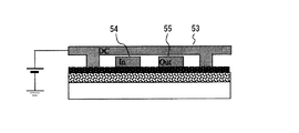
ところで、図8に示したようなMEMS構造では、振動子51と相対する下部電極52をそれぞれ入力、出力電極として機能させているが、信号を増大させようとして電極間ギャップを小さくすると、電極間の寄生容量が増大してしまい、信号の直接漏洩成分が増えてSN比を十分に確保できない可能性がある。このことから、フィルタ装置を構成するのにあたっては、例えば図9に示すように、可動構造体である振動子53とは別に、その振動子53に振動を励起するための入力電極54と、振動子53に励起された振動を検出するための出力電極55とをそれぞれ設け、振動子53に直流バイアス電圧を印加するMEMS構造とすることも考えられる。このようなMEMS構造とすれば、出力信号と寄生容量の相関を無くすことができ、SN比を十分に確保し得るようになるからである。
By the way, in the MEMS structure as shown in FIG. 8, the
しかしながら、図9に示すMEMS構造においても、可動構造体である振動子53を単独で、または複数個用いて、フィルタ装置を構成するわけであるが、その振動子53は、例えばプロセス変動やばらつき等によって長さ、幅、厚さ、物性等が変動してしまい所望の通りにならないおそれがある。したがって、その振動子53を用いたMEMS構造によりフィルタ装置を構成しても、狙い通りの透過周波数や遮断周波数等が得られないこともあり得る。
さらに、MEMS構造によるフィルタ装置では、振動子53という機械的な構造の特性を利用しているため、中心周波数の温度特性が数十〜数百ppm程度とそれほど良くない。そのため、振動子53が所望の通りに精度良く形成されている場合であっても、環境温度によっては透過周波数や遮断周波数等が変動してしまう可能性もある。
また、フィルタ装置に対しては、これを使用する際の汎用性等の観点から、同一構造で異なる仕様(中心周波数、遮断周波数、リップル、スカート特性等)に対応可能にするための技術が常に求められている。
However, even in the MEMS structure shown in FIG. 9, a filter device is configured by using a single or a plurality of
Furthermore, since the filter device having the MEMS structure uses the mechanical structure characteristic of the
In addition, for the filter device, from the viewpoint of versatility when using it, there is always technology to make it possible to handle different specifications (center frequency, cutoff frequency, ripple, skirt characteristics, etc.) with the same structure. It has been demanded.
そこで、本発明は、MEMS構造を用いた場合であっても、プロセス変動や外乱等の影響を極力受けることなく、適切な透過周波数や遮断周波数等に対応することが可能なフィルタ装置を提供することを目的とする。 Therefore, the present invention provides a filter device that can cope with an appropriate transmission frequency, cutoff frequency, and the like without being affected by process fluctuations, disturbances, and the like as much as possible even when a MEMS structure is used. For the purpose.
本発明は、上記目的を達成するために案出されたフィルタ装置である。すなわち、特定周波数帯域の信号を透過するMEMS構造のフィルタ装置であって、直流電圧が印加される可動構造体である少なくとも一つの振動子と、前記振動子に振動を励起するための入力電極と、前記振動子に励起された振動を検出するための出力電極とを有してなる振動子群を複数備え、前記複数の振動子群は、第一の振動子群、第二の振動子群および第三の振動子群からなり、前記第一の振動子群、前記第二の振動子群および前記第三の振動子群における各振動子は、それぞれが異なる中心周波数に対応したものであり、前記各振動子が対応する中心周波数から特定される周波数帯域に信号を透過するように、前記第一の振動子群がシリーズ側に位置し、前記第二の振動子群および前記第三の振動子群がシャント側に位置して、それぞれが電気的に接続されており、前記第一の振動子群、前記第二の振動子群および前記第三の振動子群のそれぞれには、当該振動子群における振動子への印加電圧の値を連続可変させる電圧調整手段が設けられているものである。 The present invention is a filter device devised to achieve the above object. That is, a MEMS-structured filter device that transmits a signal in a specific frequency band, and at least one vibrator that is a movable structure to which a DC voltage is applied, and an input electrode for exciting the vibrator A plurality of transducer groups having output electrodes for detecting vibrations excited by the transducers, wherein the plurality of transducer groups are a first transducer group and a second transducer group and made from the third transducer groups, the first group of transducers, the respective second transducer in the transducer group and the third group of transducers of the their respective is corresponding to different center frequencies The first transducer group is positioned on the series side so that each transducer transmits a signal to a frequency band specified from the corresponding center frequency, and the second transducer group and the The third transducer group is located on the shunt side and Each of the first vibrator group, the second vibrator group, and the third vibrator group is electrically connected, and a voltage applied to the vibrator in the vibrator group is connected to each of the first vibrator group, the second vibrator group, and the third vibrator group. Voltage adjusting means for continuously varying the value of is provided.
上記構成のフィルタ装置は、第一の振動子群、第二の振動子群および第三の振動子群のそれぞれが、いずれも、電圧調整手段を備えていることから、その電圧調整手段によって振動子への印加電圧の値を可変させることができる。
ここで、一般に、振動子に直流電圧を印加すると、振動子と下部電極(入力電極または出力電極)が当接する電圧に向けて徐々に共振周波数が下がっていくが、その度合いは当接電圧に近づくにつれて大きくなっていく。これは、静電バネのソフトニング効果によるものである。つまり、例えば電圧を余計に印加することで共振周波数を低周波側に変化させたり、また印加する電圧を抑えることで共振周波数を高周波側に変化させたりすることが可能となる。
したがって、振動子への印加電圧の値を可変させれば、その振動子における共振周波数が想定した共振周波数と異なる場合であっても、その相違の修正が行えるようになる。
In the filter device having the above-described configuration, each of the first vibrator group, the second vibrator group, and the third vibrator group includes a voltage adjustment unit. The value of the voltage applied to the child can be varied.
Here, in general, when a DC voltage is applied to the vibrator, the resonance frequency gradually decreases toward the voltage at which the vibrator and the lower electrode (input electrode or output electrode) come into contact with each other. It gets bigger as you get closer. This is due to the softening effect of the electrostatic spring. That is, for example, it is possible to change the resonance frequency to the low frequency side by applying an extra voltage, or to change the resonance frequency to the high frequency side by suppressing the applied voltage.
Accordingly, if the value of the voltage applied to the vibrator is varied, the difference can be corrected even when the resonance frequency of the vibrator is different from the assumed resonance frequency.
本発明のフィルタ装置によれば、振動子への印加電圧の値を可変させることで、その振動子における共振周波数を適宜修正し得るようになる。つまり、プロセス変動やばらつき、環境温度といった外乱等によって狙い通りの透過周波数や遮断周波数等が得られない場合であっても、振動子への印加電圧の値を可変させて修正することで、所望の透過周波数や遮断周波数等を実現し得るようになる。
したがって、本発明のフィルタ装置では、MEMS構造を用いた場合であっても、プロセス変動や外乱等の影響を極力受けることなく、適切な透過周波数や遮断周波数等に対応することが可能となる。
According to the filter device of the present invention, by changing the value of the voltage applied to the vibrator, the resonance frequency in the vibrator can be appropriately corrected. In other words, even if the desired transmission frequency, cutoff frequency, etc. cannot be obtained due to disturbances such as process fluctuations and variations, environmental temperature, etc., it is possible to change the value of the voltage applied to the vibrator and modify it as desired. The transmission frequency, the cut-off frequency, etc. can be realized.
Therefore, in the filter device of the present invention, even when the MEMS structure is used, it is possible to cope with an appropriate transmission frequency, cutoff frequency, and the like without being affected by process fluctuations, disturbances, and the like as much as possible.
以下、図面に基づき本発明に係るフィルタ装置について説明する。 Hereinafter, a filter device according to the present invention will be described with reference to the drawings.
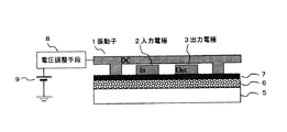
先ず、フィルタ装置の基本的な構成について説明する。図1は、本発明に係るフィルタ装置の基本的な構成例を示す説明図である。 First, the basic configuration of the filter device will be described. FIG. 1 is an explanatory diagram showing a basic configuration example of a filter device according to the present invention.
図1に示すように、ここで説明するフィルタ装置は、MEMS構造を利用して構成されたもので、直流電圧が印加される可動構造体である振動子1と、その振動子1に振動を励起するための入力電極2と、振動子1に励起された振動を検出するための出力電極3とを備えている。そして、入力電極2に特定の周波数電圧が印加された場合に、例えばポリシリコン(Poly-Si)といった絶縁材料からなる振動子1の可動部分が固有振動周波数で振動し、出力電極3と振動子1の可動部との間の空間で構成されるキャパシタの容量が変化し、これが出力電極3から出力されるようになっている。これにより、フィルタ装置では、高いQ値を実現することができるのである。
これらの振動子1、入力電極2および出力電極3は、いずれも、例えばSi(単結晶シリコン)からなる半導体基板5上にSiO2(二酸化ケイ素)膜6およびSiN(窒化ケイ素)膜7が積層された、さらにその上方に形成されている。つまり、これらを備えてなるフィルタ装置は、半導体基板5上に形成されるものであることから、他の半導体デバイスとのインテグレーションが可能である。
また、振動子1には、直流電圧が印加されることから、出力信号と寄生容量の相関を無くすことができ、SN比を十分に確保することが可能となる。
なお、振動子1は、必ずしも単独である必要はなく、複数が組み合わされてなるもの、すなわち振動子群を構成するものであってもよい。
As shown in FIG. 1, the filter device described here is configured using a MEMS structure, and a vibrator 1 which is a movable structure to which a DC voltage is applied, and a vibration is applied to the vibrator 1. An input electrode 2 for excitation and an output electrode 3 for detecting vibration excited by the vibrator 1 are provided. When a specific frequency voltage is applied to the input electrode 2, the movable part of the vibrator 1 made of an insulating material such as polysilicon (Poly-Si) vibrates at the natural vibration frequency, and the output electrode 3 and the vibrator The capacitance of the capacitor formed by the space between the movable part 1 is changed and output from the output electrode 3. Thereby, a high Q value can be realized in the filter device.
Each of the vibrator 1, the input electrode 2, and the output electrode 3 is formed by laminating a SiO 2 (silicon dioxide) film 6 and a SiN (silicon nitride) film 7 on a semiconductor substrate 5 made of, for example, Si (single crystal silicon). It is further formed above it. That is, since the filter device including these is formed on the semiconductor substrate 5, it can be integrated with other semiconductor devices.
Further, since a DC voltage is applied to the vibrator 1, the correlation between the output signal and the parasitic capacitance can be eliminated, and a sufficient SN ratio can be ensured.
The vibrator 1 does not necessarily need to be a single element, and may be a combination of a plurality of vibrators, that is, a vibrator group.
さらに、ここで説明するフィルタ装置は、その特徴的な構成として、電圧調整手段8を備えている。
電圧調整手段8は、振動子1とその振動子1への電圧の印加を行うための電源9との間に配設されたもので、振動子1への印加電圧の値を可変させるためのものである。具体的には、ボリュームやレギュレータ等を用いて構成することが考えられるが、その詳細については公知技術を利用すればよいため、ここではその説明を省略する。
Furthermore, the filter device described here includes voltage adjusting means 8 as a characteristic configuration.
The voltage adjusting means 8 is disposed between the vibrator 1 and a power source 9 for applying a voltage to the vibrator 1 and varies the value of the voltage applied to the vibrator 1. Is. Specifically, a configuration using a volume, a regulator, or the like is conceivable, but details thereof are omitted here because a known technique may be used.
このような構成のフィルタ装置では、電圧調整手段8を備えていることから、その電圧調整手段8によって振動子1への印加電圧の値を可変させることができ、これによりその振動子1における共振周波数を適宜修正し得るようになる。
Since the filter device having such a configuration includes the
ここで、振動子1への印加電圧と、その振動子1における共振周波数または振幅との関係について簡単に説明する。図2は、印加電圧と共振周波数または振幅との関係の一具体例を示す説明図である。
上述した構成のフィルタ装置において、振動子1に直流電圧を印加すると、図2(a)に示すように、振動子1と入力電極2または出力電極3といった下部電極とが当接する電圧(図中におけるA部参照)に向けて、徐々に共振周波数が下がっていく。その度合いは、当接電圧に近づくにつれて大きくなっていく。これは、振動子1において、静電バネのソフトニング効果が作用することによるものである。
つまり、例えば図中において、印加する直流電圧の値を「V0」から「+ΔV」だけ大きくすれば、振動子1における共振周波数が「f0」から「−Δf」だけ低周波側に変化し、直流電圧の値を「V0」から「−ΔV」だけ小さくすれば、振動子1における共振周波数が「f0」から「+Δf」だけ高周波側に変化することになる。
また、図2(b)に示すように、印加する直流電圧の値によっては、振動子1の振幅も変化する。例えば、直流電圧の値を大きくすれば、共振周波数の変化に伴って、振動子1の振幅が大きくなるといった具合である。
Here, the relationship between the voltage applied to the vibrator 1 and the resonance frequency or amplitude of the vibrator 1 will be briefly described. FIG. 2 is an explanatory diagram showing a specific example of the relationship between the applied voltage and the resonance frequency or amplitude.
In the filter device having the above-described configuration, when a DC voltage is applied to the vibrator 1, as shown in FIG. 2A, a voltage at which the vibrator 1 and the lower electrode such as the input electrode 2 or the output electrode 3 come into contact (in the drawing) The resonance frequency gradually decreases toward the part A). The degree increases as the contact voltage is approached. This is because the softening effect of the electrostatic spring acts on the vibrator 1.
That is, for example, in the figure, if the value of the DC voltage to be applied is increased from “V0” by “+ ΔV”, the resonance frequency in the vibrator 1 changes from “f0” to “−Δf” to the low frequency side. If the voltage value is reduced from “V0” by “−ΔV”, the resonance frequency of the vibrator 1 changes from “f0” to “+ Δf” to the high frequency side.
Further, as shown in FIG. 2B, the amplitude of the vibrator 1 also changes depending on the value of the applied DC voltage. For example, if the value of the DC voltage is increased, the amplitude of the vibrator 1 increases as the resonance frequency changes.
以上のようなソフトニング効果の影響によって、上述した構成のフィルタ装置における振動子1に対して、その印加電圧の値を電圧調整手段8が可変させれば、その振動子1における共振周波数を適宜修正し得るようになるのである。具体的には、振動子1に対して、想定した共振周波数よりも実際の共振周波数が高い場合は印加電圧の値を大きくし、実際の共振周波数が低い場合には印加電圧の値を小さくなるように抑えることで、振動子1における実際の共振周波数を想定した共振周波数に合わせられる。つまり、電圧調整手段8を介して振動子1に適切な直流バイアス電圧を印加することで、その振動子1が透過させる透過周波数または遮断する遮断周波数を適宜調整できるようになる。 If the voltage adjusting means 8 changes the value of the applied voltage with respect to the vibrator 1 in the filter device having the above-described configuration due to the influence of the softening effect as described above, the resonance frequency in the vibrator 1 is appropriately set. It can be corrected. Specifically, for the vibrator 1, the value of the applied voltage is increased when the actual resonance frequency is higher than the assumed resonance frequency, and the value of the applied voltage is decreased when the actual resonance frequency is low. By suppressing in this way, the actual resonance frequency of the vibrator 1 can be adjusted to the assumed resonance frequency. That is, by applying an appropriate DC bias voltage to the vibrator 1 via the voltage adjusting means 8, the transmission frequency transmitted by the vibrator 1 or the cutoff frequency to be cut off can be appropriately adjusted.
電圧調整手段8を介した周波数調整は、以下に述べるようにして行えばよい。
例えば、フィルタ装置を動作させた状態で、出力電極3にて検出された振動、すなわち出力電極3からの出力信号を、公知の波形検出装置等を用いてモニタリングし、そのモニタリングの結果に基づいて電圧調整手段8におけるボリューム等を作業員の人手により調整することで、振動子1への印加電圧の値を適宜可変させることが考えられる。このような周波数調整は、フィルタ装置の製造工程の最終段階にて行われる初期チューニングに適用するのが望ましい。当該周波数調整を行うようにすれば、初期チューニングによって、プロセス変動等に起因する製造ばらつきを抑えることができるからである。
また、例えば、フィルタ装置に公知の温度補償回路を付設し、その温度補償回路からの出力信号に応じて電圧調整手段8が振動子1への印加電圧の値を自動的に可変させる、いわゆるフィードバック制御を行うことで、電圧調整手段8を介した周波数調整を行うことも考えられる。このような周波数調整は、フィルタ装置の使用段階での周波数チューニングに適用するのが望ましい。当該周波数調整を行うようにすれば、環境温度の変化等といった外乱に対しても安定した動作が可能なフィルタ特性を得ることができるからである。
The frequency adjustment via the voltage adjustment means 8 may be performed as described below.
For example, in a state where the filter device is operated, vibration detected by the output electrode 3, that is, an output signal from the output electrode 3 is monitored using a known waveform detection device or the like, and based on the monitoring result It is conceivable that the value of the voltage applied to the vibrator 1 can be varied as appropriate by adjusting the volume or the like in the voltage adjusting means 8 manually by an operator. Such frequency adjustment is desirably applied to initial tuning performed at the final stage of the manufacturing process of the filter device. This is because if the frequency adjustment is performed, the initial tuning can suppress the manufacturing variation caused by the process variation and the like.
Further, for example, a known temperature compensation circuit is attached to the filter device, and the voltage adjusting means 8 automatically changes the value of the voltage applied to the vibrator 1 in accordance with the output signal from the temperature compensation circuit, so-called feedback. It is also conceivable to perform frequency adjustment via the voltage adjusting means 8 by performing control. Such frequency adjustment is preferably applied to frequency tuning in the use stage of the filter device. This is because, if the frequency adjustment is performed, it is possible to obtain filter characteristics capable of stable operation against disturbances such as changes in the environmental temperature.
次に、以上のような基本的な構成を備えた本発明に係るフィルタ装置について、具体例を挙げてさらに詳しく説明する。
図3は、本発明に係るフィルタ装置の第1の具体的な構成例を示す説明図である。図例は、反共振を持つ振動子を備えて構成された帯域透過型のフィルタ装置の一具体例を示している。
Next, the filter device according to the present invention having the basic configuration as described above will be described in more detail with specific examples.
FIG. 3 is an explanatory diagram showing a first specific configuration example of the filter device according to the present invention. The figure shows a specific example of a band-pass filter device configured with a vibrator having anti-resonance.
図3(a)に示すように、ここで説明するフィルタ装置は、複数の振動子群、すなわち第一の振動子群11と第二の振動子群12とを備えている。
これら第一の振動子群11および第二の振動子群12は、いずれも、上述した基本的な構成、すなわち振動子、入力電極、出力電極および電圧調整手段を有してなるものである。ただし、振動子は、少なくとも一つを有していれば、単独のものであっても、あるいは複数の組み合わせからなるものであってもよい。また、電圧調整手段は、第一の振動子群11と第二の振動子群12の少なくとも一方が有していれば、必ずしも両方が有していなくともよい。
As shown in FIG. 3A, the filter device described here includes a plurality of transducer groups, that is, a
Each of the
このような第一の振動子群11および第二の振動子群12における各振動子は、反共振を持つもの、すなわち図3(b)に示すような波形特性に対応したものである。ただし、第一の振動子群11と第二の振動子群12とは、それぞれが異なる中心周波数に対応したものである。つまり、反共振を持つものであっても、それぞれにおける振動子は、対応する中心周波数が異なるように形成されている。なお、反共振を持つ振動子については、公知技術を利用して実現すればよいため、ここではその説明を省略する。
Each transducer in the
そして、これら第一の振動子群11および第二の振動子群12は、図3(a)に示すように、第一の振動子群11がシリーズ側に位置し、第二の振動子群12がシャント側に位置するように、それぞれが電気的に接続されている。これにより、第一の振動子群11および第二の振動子群12は、図3(c)に示すように、それぞれの振動子の反共振のピークの大きさや中心周波数等に応じた周波数帯域の信号を透過させるフィルタ装置を構成することになる。換言すると、第一の振動子群11および第二の振動子群12は、それぞれの振動子が対応する中心周波数から特定される周波数帯域の信号を透過させるべく、一方がシリーズ側に、他方がシャント側に位置するように、それぞれ電気的に接続されているのである。
As shown in FIG. 3A, the
このように構成されたフィルタ装置では、透過させる周波数帯域が第一の振動子群11および第二の振動子群12における各振動子の特性に依存する。そのため、例えば、雰囲気温度が上がると振動子を構成する部品が膨張してしまい、各振動子の共振周波数が低くなるといったことが起こり得る。
ところが、上述した構成のフィルタ装置では、第一の振動子群11および第二の振動子群12が電圧調整手段を有していることから、各振動子に印加する直流電圧(図3(a)中におけるDC1,DC2参照)を可変させることでソフトニング効果を起こし、それぞれにおける共振周波数を図3(c)中の左右方向にシフトさせて、雰囲気温度が上がった場合であっても想定した周波数帯域を確保するといったことが可能となる。これは、雰囲気温度が下がった場合についても、全く同様である。
In the filter device configured as described above, the frequency band to be transmitted depends on the characteristics of each transducer in the
However, in the filter device having the above-described configuration, since the
つまり、第一の振動子群11および第二の振動子群12が電圧調整手段を有していることによって、その第一の振動子群11および第二の振動子群12が電気的に接続されてなるフィルタ装置では、ソフトニング効果による現象を利用して、透過させる周波数帯域の幅を広げたり、狭めたり、高周波側または低周波側にシフトさせるといった、周波数調整を行うことが可能となる。さらには、リップルの調整やアイソレーション特性等の改善を見込むことができるようになる。
したがって、プロセス変動やばらつき、雰囲気温度といった外乱等によって狙い通りの周波数帯域が得られない場合であっても、振動子への印加電圧の値を可変させて修正することで、所望の周波数帯域を実現し得るようになるので、MEMS構造を用いてフィルタ装置を構成した場合であっても、プロセス変動や外乱等の影響を極力受けることなく、適切な周波数帯域に対応することが可能となる。
なお、このような効果を得るためには、第一の振動子群11と第二の振動子群12との両方が電圧調整手段を有していることが望ましいが、これらのうちのいずれか一方のみが電圧調整手段を有している場合であっても、透過させる周波数帯域の幅を調整したり、リップルの調整やアイソレーション特性等の改善を図ったりすることは可能である。
That is, since the
Therefore, even if the target frequency band cannot be obtained due to disturbances such as process fluctuations and variations, ambient temperature, etc., the desired frequency band can be adjusted by changing the value of the voltage applied to the vibrator and correcting it. Therefore, even when the filter device is configured using the MEMS structure, it is possible to cope with an appropriate frequency band without being affected by process fluctuations, disturbances, and the like as much as possible.
In order to obtain such an effect, it is desirable that both the
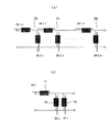
図4は、上述した第1の具体的な構成の変形例を示す説明図である。
MEMS共振子は高抵抗のデバイスなので直列接続には向いていないが、図3(a)に示した構成を基本モジュールとして、図4(a)に示すように、その基本モジュール10a,10b…10nを複数直列接続した場合であっても、各基本モジュール10a,10b…10nにおける振動子群の振動子への印加電圧の値を可変させることで、透過させる周波数帯域の幅を調整したり、リップルの調整やアイソレーション特性等の改善を図ったりすることは可能である。
さらには、図4(b)に示すように、シリーズ側の振動子群11に対して、シャント側の振動子群12a,12bの数を増やした場合についても、全く同様のことが言える。
FIG. 4 is an explanatory view showing a modification of the first specific configuration described above.
Since the MEMS resonator is a high-resistance device, it is not suitable for series connection. However, the
Further, as shown in FIG. 4B, the same applies to the case where the number of shunt-
図5は、本発明に係るフィルタ装置の第2の具体的な構成例を示す説明図である。図例は、反共振を持たない振動子を備えて構成された帯域透過型のフィルタ装置の一具体例を示している。 FIG. 5 is an explanatory diagram showing a second specific configuration example of the filter device according to the present invention. The figure shows a specific example of a band-pass filter device configured with a vibrator having no anti-resonance.
図5(a)に示すように、ここで説明するフィルタ装置は、複数の振動子群、すなわち第一の振動子群21、第二の振動子群22および第三の振動子群23を備えている。
これら第一〜第三の振動子群21〜23も、上述した基本的な構成、すなわち振動子、入力電極、出力電極および電圧調整手段を有してなるものである。ただし、振動子は、少なくとも一つを有していれば、単独のものであっても、あるいは複数の組み合わせからなるものであってもよい。また、電圧調整手段は、第一〜第三の振動子群21〜23の少なくとも一方が有していれば、必ずしも全てが有していなくともよい。
As shown in FIG. 5A, the filter device described here includes a plurality of transducer groups, that is, a
These first to
このような第一〜第三の振動子群21〜23における各振動子は、反共振を持たないもの、すなわち図5(b)に示すような波形特性に対応したものであり、それぞれが異なる中心周波数に対応したものである。つまり、それぞれにおける振動子は、対応する中心周波数が異なるように形成されている。
Each transducer in the first to
そして、これら第一〜第三の振動子群21〜23は、図5(a)に示すように、第一の振動子群21がシリーズ側に位置し、第二の振動子群22および第三の振動子群23がシャント側に位置するように、それぞれが電気的に接続されている。これにより、第一〜第三の振動子群21〜23は、図5(c)に示すように、それぞれの振動子の共振のピークの大きさや中心周波数等に応じた周波数帯域の信号を透過させるフィルタ装置を構成することになる。換言すると、第一〜第三の振動子群21〜23は、それぞれの振動子が対応する中心周波数から特定される周波数帯域の信号を透過させるべく、一つがシリーズ側に、残りがシャント側に位置するように、それぞれ電気的に接続されているのである。
As shown in FIG. 5A, the first to
このように構成されたフィルタ装置では、透過させる周波数帯域が第一〜第三の振動子群21〜23における各振動子の特性に依存するが、それぞれが電圧調整手段を有していることから、各振動子に印加する直流電圧(図5(a)中におけるDC1〜DC3参照)を可変させることでソフトニング効果を起こし、それぞれにおける共振周波数を図5(c)中の左右方向にシフトさせて、例えば雰囲気温度に変化があった場合でも想定した周波数帯域を確保するといったことが可能となる。つまり、第一〜第三の振動子群21〜23が電圧調整手段を有していることによって、その第一〜第三の振動子群21〜23が電気的に接続されてなるフィルタ装置では、ソフトニング効果による現象を利用して、透過させる周波数帯域の幅を広げたり、狭めたり、高周波側または低周波側にシフトさせるといった、周波数調整を行うことが可能となる。さらには、リップルの調整やアイソレーション特性等の改善を見込むことができるようになる。
したがって、プロセス変動やばらつき、雰囲気温度といった外乱等によって狙い通りの周波数帯域が得られない場合であっても、振動子への印加電圧の値を可変させて修正することで、所望の周波数帯域を実現し得るようになるので、MEMS構造を用いてフィルタ装置を構成した場合であっても、プロセス変動や外乱等の影響を極力受けることなく、適切な周波数帯域に対応することが可能となる。
なお、このような効果を得るためには、第一〜第三の振動子群21〜23との全てが電圧調整手段を有していることが望ましいが、これらのうちのいずれか一つのみが電圧調整手段を有している場合であっても、透過させる周波数帯域の幅を調整したり、リップルの調整やアイソレーション特性等の改善を図ったりすることは可能である。
In the filter device configured as described above, the frequency band to be transmitted depends on the characteristics of the vibrators in the first to
Therefore, even if the target frequency band cannot be obtained due to disturbances such as process fluctuations and variations, ambient temperature, etc., the desired frequency band can be adjusted by changing the value of the voltage applied to the vibrator and correcting it. Therefore, even when the filter device is configured using the MEMS structure, it is possible to cope with an appropriate frequency band without being affected by process fluctuations, disturbances, and the like as much as possible.
In order to obtain such an effect, it is desirable that all of the first to
図6は、上述した第2の具体的な構成の変形例を示す説明図である。図例のように、第一〜第三の振動子群21〜23の並べ方としては、一般的なπ型も考えられる。このような電気的接続をした場合であっても、第一〜第三の振動子群21〜23における振動子への印加電圧の値を可変させることで、透過させる周波数帯域の幅を調整したり、リップルの調整やアイソレーション特性等の改善を図ったりすることが可能である。
FIG. 6 is an explanatory diagram showing a modification of the second specific configuration described above. As shown in the figure, a general π type is also conceivable as a way of arranging the first to
図7は、本発明に係るフィルタ装置の第3の具体的な構成例を示す説明図である。図例は、反共振を持たない振動子を備えて構成された帯域遮断型のフィルタ装置の一具体例を示している。
図例のように、ここで説明するフィルタ装置は、一つの振動子群31がシャント側に配置されてなるものである。振動子群31は、上述した基本的な構成、すなわち振動子、入力電極、出力電極および電圧調整手段を有してなるものである。ただし、振動子は、少なくとも一つを有していれば、単独のものであっても、あるいは複数の組み合わせからなるものであってもよい。このような振動子群31における振動子は、上述した実施例2の場合と同様に、反共振を持たないものである。これにより、振動子群31は、その振動子群31における振動子の共振のピークの大きさや中心周波数等に応じた周波数帯域の信号を遮断するフィルタ装置を構成することになる。
FIG. 7 is an explanatory diagram showing a third specific configuration example of the filter device according to the present invention. The figure shows a specific example of a band cut-off filter device configured with a vibrator having no anti-resonance.
As shown in the figure, the filter device described here has one transducer group 31 arranged on the shunt side. The vibrator group 31 includes the basic configuration described above, that is, the vibrator, the input electrode, the output electrode, and the voltage adjusting unit. However, the vibrator may be a single vibrator or a combination of a plurality of vibrators as long as at least one vibrator is provided. The vibrators in such a vibrator group 31 do not have anti-resonance as in the case of the second embodiment described above. Thus, the vibrator group 31 constitutes a filter device that cuts off a signal in a frequency band corresponding to the magnitude of the resonance peak of the vibrator, the center frequency, and the like in the vibrator group 31.
このように構成されたフィルタ装置では、遮断する周波数帯域が振動子群31における振動子の特性に依存することになるが、その振動子群31が電圧調整手段を有していることから、振動子に印加する直流電圧(図7中におけるDC参照)を可変させることでソフトニング効果を起こし、その共振周波数をシフトさせるといったことが可能となる。つまり、振動子群31が電圧調整手段を有していることによって、その振動子群31が電気的に接続されてなるフィルタ装置では、ソフトニング効果による現象を利用して、遮断する周波数帯域を高周波側または低周波側にシフトさせるといった、周波数調整を行うことが可能となる。さらには、リップルの調整やアイソレーション特性等の改善を見込むことができるようになる。
したがって、プロセス変動やばらつき、雰囲気温度といった外乱等によって狙い通りの周波数帯域が得られない場合であっても、振動子への印加電圧の値を可変させて修正することで、所望の周波数帯域を実現し得るようになるので、MEMS構造を用いてフィルタ装置を構成した場合であっても、プロセス変動や外乱等の影響を極力受けることなく、適切な周波数帯域に対応することが可能となる。
In the filter device configured as described above, the frequency band to be cut off depends on the characteristics of the vibrators in the vibrator group 31. Since the vibrator group 31 has voltage adjusting means, By varying the DC voltage applied to the child (see DC in FIG. 7), it is possible to cause a softening effect and shift its resonance frequency. That is, in the filter device in which the vibrator group 31 has the voltage adjusting means and the vibrator group 31 is electrically connected, the frequency band to be cut off is utilized by utilizing the phenomenon due to the softening effect. It is possible to perform frequency adjustment such as shifting to a high frequency side or a low frequency side. Furthermore, it is possible to expect improvements in ripple adjustment and isolation characteristics.
Therefore, even if the target frequency band cannot be obtained due to disturbances such as process fluctuations and variations, ambient temperature, etc., the desired frequency band can be adjusted by changing the value of the voltage applied to the vibrator and correcting it. Therefore, even when the filter device is configured using the MEMS structure, it is possible to cope with an appropriate frequency band without being affected by process fluctuations, disturbances, and the like as much as possible.
なお、当然のことではあるが、上述した実施例1〜3は、本発明の好適な一実施具体例に過ぎず、本発明がこれに限定されるものでないことは勿論である。 Needless to say, the above-described first to third embodiments are merely preferred specific examples of the present invention, and the present invention is of course not limited thereto.
1…振動子、2…入力電極、3…出力電極、8…電圧調整手段、11、21…第一の振動子群、12,12a,12b、22…第二の振動子群、23…第三の振動子群、31…振動子群 DESCRIPTION OF SYMBOLS 1 ... Vibrator, 2 ... Input electrode, 3 ... Output electrode, 8 ... Voltage adjustment means, 11, 21 ... First vibrator group, 12, 12a, 12b, 22 ... Second vibrator group, 23 ... First Three vibrator groups, 31 ... vibrator group
Claims (1)
直流電圧が印加される可動構造体である少なくとも一つの振動子と、前記振動子に振動を励起するための入力電極と、前記振動子に励起された振動を検出するための出力電極とを有してなる振動子群を複数備え、
前記複数の振動子群は、第一の振動子群、第二の振動子群および第三の振動子群からなり、
前記第一の振動子群、前記第二の振動子群および前記第三の振動子群における各振動子は、それぞれが異なる中心周波数に対応したものであり、
前記各振動子が対応する中心周波数から特定される周波数帯域に信号を透過するように、前記第一の振動子群がシリーズ側に位置し、前記第二の振動子群および前記第三の振動子群がシャント側に位置して、それぞれが電気的に接続されており、
前記第一の振動子群、前記第二の振動子群および前記第三の振動子群のそれぞれには、当該振動子群における振動子への印加電圧の値を連続可変させる電圧調整手段が設けられている
フィルタ装置。 A MEMS filter device that transmits a signal in a specific frequency band,
At least one vibrator that is a movable structure to which a DC voltage is applied, an input electrode for exciting vibration to the vibrator, and an output electrode for detecting vibration excited by the vibrator A plurality of vibrator groups,
The plurality of transducer groups include a first transducer group, a second transducer group, and a third transducer group,
The first group of transducers, the respective second transducer in the transducer groups and the third transducer groups of are those their respective has corresponding to different center frequencies,
The first vibrator group is positioned on the series side so that each vibrator transmits a signal in a frequency band specified from a corresponding center frequency, and the second vibrator group and the third vibration group The child group is located on the shunt side and each is electrically connected,
Each of the first vibrator group, the second vibrator group, and the third vibrator group is provided with voltage adjusting means for continuously varying the value of the voltage applied to the vibrator in the vibrator group. The filter device.
Priority Applications (1)
| Application Number | Priority Date | Filing Date | Title |
|---|---|---|---|
| JP2003316248A JP4442167B2 (en) | 2003-09-09 | 2003-09-09 | Filter device |
Applications Claiming Priority (1)
| Application Number | Priority Date | Filing Date | Title |
|---|---|---|---|
| JP2003316248A JP4442167B2 (en) | 2003-09-09 | 2003-09-09 | Filter device |
Publications (3)
| Publication Number | Publication Date |
|---|---|
| JP2005086469A JP2005086469A (en) | 2005-03-31 |
| JP2005086469A5 JP2005086469A5 (en) | 2006-06-29 |
| JP4442167B2 true JP4442167B2 (en) | 2010-03-31 |
Family
ID=34416206
Family Applications (1)
| Application Number | Title | Priority Date | Filing Date |
|---|---|---|---|
| JP2003316248A Expired - Fee Related JP4442167B2 (en) | 2003-09-09 | 2003-09-09 | Filter device |
Country Status (1)
| Country | Link |
|---|---|
| JP (1) | JP4442167B2 (en) |
Families Citing this family (7)
| Publication number | Priority date | Publication date | Assignee | Title |
|---|---|---|---|---|
| JP2007174438A (en) * | 2005-12-23 | 2007-07-05 | Toshiba Corp | Filter circuit and radio communication system with filter |
| JP2008132583A (en) | 2006-10-24 | 2008-06-12 | Seiko Epson Corp | Mems device |
| CN101168434B (en) * | 2006-10-24 | 2011-06-15 | 精工爱普生株式会社 | MEMS device |
| JP5505596B2 (en) * | 2008-06-18 | 2014-05-28 | セイコーエプソン株式会社 | Resonant circuit, oscillation circuit, filter circuit, and electronic device |
| JP5169518B2 (en) * | 2008-06-18 | 2013-03-27 | セイコーエプソン株式会社 | RESONANT CIRCUIT, ITS MANUFACTURING METHOD, AND ELECTRONIC DEVICE |
| JP2012195829A (en) | 2011-03-17 | 2012-10-11 | Seiko Epson Corp | Oscillation circuit |
| JP2012222718A (en) | 2011-04-13 | 2012-11-12 | Seiko Epson Corp | Oscillator |
-
2003
- 2003-09-09 JP JP2003316248A patent/JP4442167B2/en not_active Expired - Fee Related
Also Published As
| Publication number | Publication date |
|---|---|
| JP2005086469A (en) | 2005-03-31 |
Similar Documents
| Publication | Publication Date | Title |
|---|---|---|
| US7511870B2 (en) | Highly tunable low-impedance capacitive micromechanical resonators, oscillators, and processes relating thereto | |
| US6909221B2 (en) | Piezoelectric on semiconductor-on-insulator microelectromechanical resonators | |
| US8253514B2 (en) | Array of coupled resonators, bandpass filter and oscillator | |
| US7876177B2 (en) | Resonator having an output electrode underneath first and second electrode arms | |
| JP5505596B2 (en) | Resonant circuit, oscillation circuit, filter circuit, and electronic device | |
| EP2282404A1 (en) | Frequency selection and amplifying device | |
| JP2002535865A (en) | Device including a micromechanical resonator having an operating frequency and method for extending the operating frequency | |
| EP3210303A1 (en) | Compound spring mems resonator for oscillators and real-time clock applications | |
| JP4617904B2 (en) | Micro vibrator, semiconductor device, and communication device | |
| JP4977431B2 (en) | Micromechanical resonator | |
| JP4442167B2 (en) | Filter device | |
| US6853041B2 (en) | Micro-machined coupled capacitor devices | |
| JP5105345B2 (en) | Oscillator | |
| JP4710435B2 (en) | Microresonator, bandpass filter, semiconductor device, and communication device | |
| JP2007013447A5 (en) | ||
| JP2009088685A (en) | Electromechanical element, and semiconductor device | |
| JP4965962B2 (en) | Micromechanical resonator | |
| JP4341288B2 (en) | MEMS resonator, method of manufacturing the same, and filter | |
| US8373513B2 (en) | Compensated micro/nano-resonator with improved capacitive detection and method for producing same | |
| Yan et al. | Narrow bandwidth single-resonator MEMS tuning fork filter | |
| JP4930769B2 (en) | Oscillator | |
| JP4415616B2 (en) | Micro machine | |
| JP2009118331A (en) | Electric machine filter | |
| JP5081586B2 (en) | Micromechanical resonator | |
| US6965274B2 (en) | Thin film bulk acoustic resonator for controlling resonance frequency and voltage controlled oscillator using the same |
Legal Events
| Date | Code | Title | Description |
|---|---|---|---|
| A521 | Written amendment |
Free format text: JAPANESE INTERMEDIATE CODE: A523 Effective date: 20060512 |
|
| A621 | Written request for application examination |
Free format text: JAPANESE INTERMEDIATE CODE: A621 Effective date: 20060512 |
|
| A977 | Report on retrieval |
Free format text: JAPANESE INTERMEDIATE CODE: A971007 Effective date: 20090615 |
|
| A131 | Notification of reasons for refusal |
Free format text: JAPANESE INTERMEDIATE CODE: A131 Effective date: 20090623 |
|
| A521 | Written amendment |
Free format text: JAPANESE INTERMEDIATE CODE: A523 Effective date: 20090818 |
|
| A131 | Notification of reasons for refusal |
Free format text: JAPANESE INTERMEDIATE CODE: A131 Effective date: 20091006 |
|
| RD02 | Notification of acceptance of power of attorney |
Free format text: JAPANESE INTERMEDIATE CODE: A7422 Effective date: 20091007 |
|
| RD04 | Notification of resignation of power of attorney |
Free format text: JAPANESE INTERMEDIATE CODE: A7424 Effective date: 20091015 |
|
| A521 | Written amendment |
Free format text: JAPANESE INTERMEDIATE CODE: A523 Effective date: 20091127 |
|
| TRDD | Decision of grant or rejection written | ||
| A01 | Written decision to grant a patent or to grant a registration (utility model) |
Free format text: JAPANESE INTERMEDIATE CODE: A01 Effective date: 20091222 |
|
| A01 | Written decision to grant a patent or to grant a registration (utility model) |
Free format text: JAPANESE INTERMEDIATE CODE: A01 |
|
| A61 | First payment of annual fees (during grant procedure) |
Free format text: JAPANESE INTERMEDIATE CODE: A61 Effective date: 20100104 |
|
| FPAY | Renewal fee payment (event date is renewal date of database) |
Free format text: PAYMENT UNTIL: 20130122 Year of fee payment: 3 |
|
| LAPS | Cancellation because of no payment of annual fees |