JP4435663B2 - Solder material, electronic component, and method of manufacturing electronic component - Google Patents
Solder material, electronic component, and method of manufacturing electronic component Download PDFInfo
- Publication number
- JP4435663B2 JP4435663B2 JP2004291979A JP2004291979A JP4435663B2 JP 4435663 B2 JP4435663 B2 JP 4435663B2 JP 2004291979 A JP2004291979 A JP 2004291979A JP 2004291979 A JP2004291979 A JP 2004291979A JP 4435663 B2 JP4435663 B2 JP 4435663B2
- Authority
- JP
- Japan
- Prior art keywords
- solder
- electronic component
- solder material
- component
- substrate
- Prior art date
- Legal status (The legal status is an assumption and is not a legal conclusion. Google has not performed a legal analysis and makes no representation as to the accuracy of the status listed.)
- Expired - Fee Related
Links
Images


Description
本発明は、配線基板上に表面実装部品を実装した電子部品、特に表面実装部品を封止した電子部品に好適なはんだ材料、このはんだ材料を含んだ電子部品及びこのはんだ材料を用いた電子部品の製造方法に関する。 The present invention relates to a solder material suitable for an electronic component in which a surface mount component is mounted on a wiring board, in particular, an electronic component in which the surface mount component is sealed, an electronic component including the solder material, and an electronic component using the solder material. It relates to the manufacturing method.
セラミックコンデンサやSAW(表面波)素子チップなどのような小型の電子部品(この明細書では表面実装部品と呼ぶ)はプリント配線基板等の基板に実装された後、湿気や搬送時の衝撃等による破壊を防ぐために封止されることで1つの電子部品ユニット(この明細書ではこのユニットを電子部品と呼ぶ)として取り扱われる場合がある。封止は、例えばエポキシ樹脂を主成分とした熱硬化性成形材料を、基板上に総ての当該表面実装部品群の表面全体が覆われるように供給した後、当該成形材料を硬化させることにより行われている。 Small electronic components (referred to as surface mount components in this specification) such as ceramic capacitors and SAW (surface wave) element chips are mounted on a substrate such as a printed wiring board, and then are subjected to moisture or impact during transportation. In some cases, it is handled as one electronic component unit (this unit is referred to as an electronic component in this specification) by being sealed to prevent destruction. Sealing is performed by, for example, supplying a thermosetting molding material mainly composed of an epoxy resin so that the entire surface of the surface mount component group is covered on the substrate, and then curing the molding material. Has been done.
表面実装部品を基板に実装させる方法として、現在はリフロー法が広く用いられている。リフロー法とは、あらかじめ基板上にはんだペーストやクリームはんだなどと呼ばれているペースト状のはんだ材料を、基板のパターンに合わせて印刷、又はディスペンスすることで付着させておいた後、当該はんだ材料上に表面実装部品を載置し、当該基板をリフロー炉と呼ばれる加熱炉内に搬入する。基板がリフロー炉内を通過する間に、炉内の熱により、基板上に成膜されたはんだが溶融されることで、電子部品の基板へのはんだ付けを行う方法である。この方法によれば、電子部品を一度に同一の基板にはんだ付けすることができるため、基板上に高密度に電子部品を配置することが可能である。 Currently, the reflow method is widely used as a method of mounting surface-mounted components on a substrate. The reflow method is a method in which a paste-like solder material called solder paste or cream solder is attached to a substrate in advance by printing or dispensing according to the pattern of the substrate, and then the solder material. A surface-mounted component is placed on the substrate, and the substrate is carried into a heating furnace called a reflow furnace. In this method, the solder formed on the substrate is melted by the heat in the furnace while the substrate passes through the reflow furnace, thereby soldering the electronic component to the substrate. According to this method, since the electronic components can be soldered to the same substrate at a time, it is possible to arrange the electronic components on the substrate at a high density.
携帯電話等の電子機器の組み立て工程においては、上記のように作成された多数の電子部品が基板に実装される。この工程における電子部品の基板実装も上述のような利点があることからリフロー法により行われることが多い。 In an assembly process of an electronic device such as a mobile phone, a large number of electronic components created as described above are mounted on a substrate. The board mounting of electronic components in this process is also often performed by the reflow method because of the advantages described above.
しかし、リフロー法は前述の通りリフロー炉を用いて、はんだが溶ける程度の熱を基板周囲から与えることによって、はんだ付けを行う方法であるため、電子部品が載置された基板が炉内を通過する際に基板上のはんだのみならず当該電子部品も加熱されることになる。 However, since the reflow method is a method of soldering by applying heat from the periphery of the substrate to the extent that the solder melts using the reflow furnace as described above, the substrate on which the electronic component is placed passes through the furnace. In this case, not only the solder on the board but also the electronic component is heated.
以下、図5を参照しながら電子部品内部における、表面実装部品を基板に固着したはんだが変化する様子を説明する。図5(a)は電子部品がリフロー炉内に搬入される前の状態を示している。この時点においては、はんだ材料41は、表面実装部品3Aの両端の電極32と、基板21上に形成されている電極であるマウントパッド22とを接合することで、基板21上に表面実装部品3Aを固着しかつ電極32,22間を電気的に接合している。また、表面実装部品3Aの周囲は封止材料51により覆われている。電子部品がリフロー炉内に入り、加熱されると前記はんだ材料41も加熱される。はんだ材料41は加熱され溶融されることで体積膨張して、図5(b)に示すように、表面実装部品3Aが接合されている基板21の表面及び表面実装部品3Aと、封止材料51との間の界面に拡がり、表面実装部品3Aの電極32、32間を短絡するなどして故障に至るおそれがある。
Hereinafter, with reference to FIG. 5, a state in which the solder that fixes the surface mounting component to the substrate inside the electronic component will be described. FIG. 5A shows a state before the electronic component is carried into the reflow furnace. At this time, the
上記のようなはんだ材料の再加熱時における不具合を防ぐために、再加熱時の温度で軟化する封止材料を用いることが検討されている。この場合、上述のように電子部品を基板に接合しているはんだ材料が溶融されて膨張したときに、その体積膨張に合わせて、電子部品を被覆している封止材料が変形することで、上記の基板表面及び電子部品と、封止材料との間の界面に前記はんだが拡がることが抑制されることが期待される。 In order to prevent the trouble at the time of reheating the solder material as described above, it has been studied to use a sealing material that softens at the temperature at the time of reheating. In this case, when the solder material joining the electronic component to the substrate as described above is melted and expanded, the sealing material covering the electronic component is deformed in accordance with the volume expansion, It is expected that the solder is prevented from spreading at the interface between the substrate surface and the electronic component and the sealing material.
しかしその方法は、基板に実装された電子部品の密度が高い場合や、封止材料に含まれた樹脂の吸湿度が高い場合に、十分な効果を発揮できないという欠点を有する。従って、このはんだ材料の膨張が引き起こす電子部品の不具合に対して、いまだ有効な対策はとられていないのが現状である。なおこの種のはんだ材料として、電子部品をアプリケーションに実装するときに再溶融が起こらないようにするために、はんだ材料の組成を工夫して融点を高める技術が特許文献1に記載されているが、融点が高くなるとリフロー炉の消耗が激しくなったり、部品の劣化を起こしたりする場合もあり、好ましくない。 However, this method has a drawback that a sufficient effect cannot be exhibited when the density of electronic components mounted on the substrate is high or when the moisture absorption of the resin contained in the sealing material is high. Therefore, at present, no effective measures have been taken against the malfunction of the electronic component caused by the expansion of the solder material. As this kind of solder material, Patent Document 1 discloses a technique for improving the melting point by devising the composition of the solder material in order to prevent remelting when mounting an electronic component in an application. If the melting point is high, the reflow furnace may be exhausted and parts may be deteriorated.
本発明は上記した従来技術の欠点を除くためなされたものであって、その目的とするところは、加熱溶融時における体積の膨張が少ないはんだ材料を提供することである。本発明の別の目的は、このはんだ材料を用いることにより、はんだ材料の再溶融時における故障を抑えることのできる電子部品を提供することである。本発明のさらに別の目的は、前記はんだ材料を用いて、電子部品を製造するのに好適な製造方法を提供することである。 The present invention has been made to eliminate the above-mentioned drawbacks of the prior art, and an object of the present invention is to provide a solder material having a small volume expansion during heating and melting. Another object of the present invention is to provide an electronic component that can suppress failure during remelting of the solder material by using the solder material. Still another object of the present invention is to provide a manufacturing method suitable for manufacturing an electronic component using the solder material.
本発明にかかるはんだ材料は、Snを主成分とするはんだ組成物と、少なくともその内部が前記はんだ組成物の固相線温度よりも高い固相線温度を有する金属からなる金属粉と、を混合してなり、前記はんだ組成物は、当該はんだ組成物全体の質量に対してAgを2.0〜4.0質量%、Cuを0.1〜1.5質量%夫々含み、当該はんだ組成物の残部はSnにより構成され、前記金属粉は、Cuからなる本体部と、本体部の表面を覆うAgからなる金属膜と、により構成され、前記はんだ組成物の質量に対して20〜35質量%混入されていることを特徴とする。すなわち、加熱時に金属粉が溶融し始める温度がはんだ組成物の溶融し始める温度よりも高ければよい。 The solder material according to the present invention is a mixture of a solder composition containing Sn as a main component and a metal powder made of a metal having at least a solidus temperature higher than the solidus temperature of the solder composition. The solder composition contains 2.0 to 4.0% by mass of Ag and 0.1 to 1.5% by mass of Cu with respect to the total mass of the solder composition. The remainder of the metal powder is composed of Sn, and the metal powder is composed of a main body portion made of Cu and a metal film made of Ag covering the surface of the main body portion, and 20 to 35 mass relative to the mass of the solder composition. % Is mixed. That is, the temperature at which the metal powder starts to melt during heating should be higher than the temperature at which the solder composition starts to melt.
例えば、前記はんだ組成物は粉体であり、フラックスを混合してペースト状とされていてもよい。
For example, the solder composition may be a powder and may be made into a paste by mixing a flux .
また、本発明に係る電子部品は、上記のはんだ材料を用いて表面実装部品を実装されたことを特徴とする。この電子部品は、例えば封止材料により封止されていてもよい。 An electronic component according to the present invention is characterized in that a surface-mounted component is mounted using the above solder material. This electronic component may be sealed with, for example, a sealing material.
さらに、本発明に係る電子部品の製造方法は配線基板の電極上に上述のはんだ材料を供給する工程と、はんだ材料の上に表面実装部品を載せる工程と、前記はんだ材料を加熱して溶融することにより表面実装部品の電極と配線基板の電極とを電気的に接続する工程と、前記表面部品を封止材料により封止する工程と、を含むことを特徴とする。 Furthermore, the method for manufacturing an electronic component according to the present invention includes a step of supplying the above-described solder material onto the electrodes of the wiring board, a step of placing the surface mount component on the solder material, and heating and melting the solder material. Thus, the method includes a step of electrically connecting the electrode of the surface-mounted component and the electrode of the wiring board, and a step of sealing the surface component with a sealing material.
本発明によれば、はんだ組成物が溶融したときにその溶融物の中に金属粉が溶融せずに分散した状態になるのではんだ自体つまりはんだ組成物は、金属粉の含有量だけ見かけよりも少ない。よって、はんだ材料の溶融時(金属粉は溶融しないが便宜上このような表現とする)において、当該はんだ材料の体積膨張の程度は小さくなる。このため例えば表面実装部品を配線基板に実装して封止した構造の電子部品が加熱されて内部のはんだ材料が溶融したときに、配線基板及び表面実装部品と封止材料との間の界面にはんだ材料が侵入することが抑えられるので、電極間が短絡するといった故障が起こりにくくなる。したがって電子部品を電子機器の配線基板に組み込むときやリペアーのために取り外すときなどにおいて電子部品の電極側のはんだ材料を溶融するために当該電子部品が加熱されても不良になるおそれが低減する。 According to the present invention, when the solder composition is melted, the metal powder is not melted and dispersed in the melt, so that the solder itself, that is, the solder composition, is more than the apparent amount of the metal powder. Few. Therefore, when the solder material is melted (the metal powder is not melted but expressed as such for convenience), the volume expansion of the solder material becomes small. For this reason, for example, when an electronic component having a structure in which a surface mounting component is mounted on a wiring board and sealed is heated and the internal solder material is melted, the wiring board and the interface between the surface mounting component and the sealing material are formed. Since intrusion of the solder material is suppressed, a failure such as a short circuit between the electrodes is less likely to occur. Therefore, when the electronic component is incorporated into the wiring board of the electronic device or removed for repair, the solder material on the electrode side of the electronic component is melted to reduce the possibility of being defective even if the electronic component is heated.
さらにはんだ材料をはんだ組成物の粉体とフラックスとを混合してペースト状とし、金属粉の表面部分(外層部分)をはんだ組成物となじみやすい材料により構成することにより、例えばSnを主成分とし、AgとCuとを含むはんだ組成物に対してAgあるいはSnを用いることにより、金属粉の分散性がよくなってはんだ組成物の不連続部位の発生が抑えられる。この場合Agを用いることによりAgが溶け出してはんだ材料の融点が高くなり、結果として電子部品を加熱したときにはんだ材料が溶融しにくくなるので、この点からも既述の故障が起こりにくくなる。 Furthermore, the solder material powder and flux are mixed into a paste, and the surface portion (outer layer portion) of the metal powder is made of a material that is easily compatible with the solder composition, for example, Sn as a main component. By using Ag or Sn for the solder composition containing Ag and Cu, the dispersibility of the metal powder is improved and the occurrence of discontinuous portions of the solder composition is suppressed. In this case, by using Ag, Ag melts and the melting point of the solder material becomes high. As a result, when the electronic component is heated, the solder material is difficult to melt. .
次に好ましい実施の形態を挙げて本発明に係るはんだ材料をさらに詳細に説明する。この実施形態のはんだ材料は、はんだ組成物の粉体と金属粉とフラックスとを混合してなるペースト状のはんだ材料(はんだペースト)として構成される。はんだ組成物としては、公知のまたは新規の、いずれのはんだ組成物であっても用いることができる。ところで本明細書において、はんだ組成物とは、はんだとしての役割を果たす一定の組成を持った合金のことをいう。例えばSn、Ag及びCuが金属として含有されているはんだ組成物はPbフリーのはんだとして広く用いられている。 Next, the solder material according to the present invention will be described in more detail by giving preferred embodiments. The solder material of this embodiment is configured as a paste-like solder material (solder paste) formed by mixing a powder of a solder composition, a metal powder, and a flux. As the solder composition, any known or novel solder composition can be used. By the way, in this specification, a solder composition means an alloy having a certain composition that plays a role of solder. For example, a solder composition containing Sn, Ag, and Cu as a metal is widely used as a Pb-free solder.
前記Ag及びCuが含まれているはんだ組成物において、Agの当該はんだ組成物全体に対する含有量は、2.0〜4.0質量%が好ましく、より好ましくは3.0質量%である。Cuの当該はんだ組成物全体に対する含有量は0.1〜1.5質量%が好ましく、より好ましくは0.3〜0.7%である。当該はんだ組成物の残部はSnにより構成される。ただし当該はんだ組成物には、はんだの濡れ性を改善する等の目的でFe、Ni等の金属あるいは非金属成分が適量加えられていてもよい。 In the solder composition containing Ag and Cu, the content of Ag with respect to the entire solder composition is preferably 2.0 to 4.0% by mass, and more preferably 3.0% by mass. The content of Cu with respect to the entire solder composition is preferably 0.1 to 1.5% by mass, and more preferably 0.3 to 0.7%. The balance of the solder composition is composed of Sn. However, an appropriate amount of a metal such as Fe or Ni or a non-metallic component may be added to the solder composition for the purpose of improving the wettability of the solder.
上述のはんだ組成物は、細かく砕き、粒子状にすることが好ましい。粒子が大きすぎると生成するはんだペーストの基板への印刷性が悪くなる。その一方で、粒子が小さすぎるとはんだペーストが過熱された際におけるはんだのぬれ性が悪くなる原因となる。そのため粒子の大きさは5〜50μm程度であることが好ましい。 The solder composition described above is preferably crushed into particles. If the particles are too large, the printability of the generated solder paste on the substrate will deteriorate. On the other hand, when the particles are too small, the solder wettability is deteriorated when the solder paste is overheated. Therefore, the size of the particles is preferably about 5 to 50 μm.
はんだ組成物を粒子状にする方法としては、例えばターボミル、ローラミル、金属粉ミル、遠心力粉砕機、パルベライザー等の従来公知の粉砕機を用いて、上述のはんだ組成物を適当な大きさに粉砕する等の方法を用いることができる。 As a method for making the solder composition into particles, for example, the above-described solder composition is pulverized to an appropriate size using a conventionally known pulverizer such as a turbo mill, a roller mill, a metal powder mill, a centrifugal pulverizer, or a pulverizer. Or the like can be used.
本発明に係るはんだ材料中に含まれる金属粉は、金属粉の1粒全体は同じ金属により構成されていてもよいが、粒本体を当該粒本体とは異なる金属により被覆した構成、つまり内部の本体部と表面部分とが異なる金属である、いわば複合金属粉であってもよい。 In the metal powder contained in the solder material according to the present invention, one whole of the metal powder may be made of the same metal, but the structure in which the grain body is coated with a metal different from the grain body, It may be a so-called composite metal powder in which the main body portion and the surface portion are different metals.
粒本体を本体部と呼ぶことにして説明を進めると、本体部を構成する金属としては、本発明を実施するために選択したはんだ組成物の固相線温度よりも高い固相線温度を有する金属が選択される。つまり本体部及びはんだ組成物の夫々の融点に幅がある場合において、本体部の融点の範囲中で最も低い温度がはんだ組成物の融点の範囲中で最も高い温度よりも高ければよい。さらに言い換えれば、本体部の溶け始めの温度がはんだ組成物の融点の範囲中で最も高い温度よりも高ければよい。従って、融点が高く、比較的安価なPb、Cu等の金属により当該本体部を構成することが好ましく、Cuを用いて当該本体部を構成することがより好ましい。ただし、当該本体部は単一の金属により構成されていても、複数の金属の合金により構成されていてもよい。なお本体部は、はんだ付けの際にリフロー炉などにより加熱される温度よりも高い固相線温度を有することが必要である。但しこれは装置側の問題であって加熱する温度をはんだ組成物の固相線温度にあわせて調整すればよいので、本体部の固相線温度がはんだ組成物の固相線温度よりも高ければよい。 When the description proceeds by calling the main body part of the grain, the metal constituting the main body part has a solidus temperature higher than the solidus temperature of the solder composition selected for carrying out the present invention. A metal is selected. That is, when the melting points of the main body part and the solder composition have a range, the lowest temperature in the range of the melting point of the main body part may be higher than the highest temperature in the melting point range of the solder composition. In other words, it is sufficient that the temperature at which the main body starts to melt is higher than the highest temperature in the melting point range of the solder composition. Therefore, it is preferable that the main body is made of a relatively inexpensive metal such as Pb and Cu, and the main body is more preferably made of Cu. However, the main body portion may be made of a single metal or an alloy of a plurality of metals. Note that the main body portion needs to have a solidus temperature higher than the temperature heated by a reflow furnace or the like during soldering. However, this is a problem on the device side, and it is only necessary to adjust the heating temperature in accordance with the solidus temperature of the solder composition, so that the solidus temperature of the main body is higher than the solidus temperature of the solder composition. That's fine.
上記金属の本体部の粒径の好ましい値は、はんだ組成物により多少変わってくるが、例えばSn−Ag−Cu系のはんだ組成物であれば5〜50μmであることが好ましく、より好ましくは10〜15μmである。当該本体部は、当該本体部により構成される金属粉のはんだ組成物中における分散性を向上させる目的から、球形又は略球形であることが好ましいが、表面に凹凸を持った構造であってもよい。 The preferable value of the particle size of the metal main body part varies slightly depending on the solder composition. For example, in the case of a Sn-Ag-Cu solder composition, it is preferably 5 to 50 μm, more preferably 10 ~ 15 μm. The main body part is preferably spherical or substantially spherical for the purpose of improving the dispersibility of the metal powder constituted by the main body part in the solder composition, but even if it has a structure with irregularities on the surface. Good.
本体部の表面に形成する金属膜(表面部)は、単一の金属を用いても、複数の金属からなる合金を用いてもよいが、はんだ組成物と金属粉との親和性(なじみ性)を向上させ、はんだ材料中における金属粉の分散性を向上させる利点が得られることから、前記はんだ組成物中に含まれる金属と同一の金属が用いられることが好ましい。親和性が強いとは、金属間化合物を生成する作用があることを意味し、より具体的には金属粉がほとんど凝集せずにはんだ組成物中に分散している状態が得られることをいう。例えば、Sn−3・0Ag−0.5Cuはんだ(はんだ合金全体に対して夫々Agが3.0質量%、Cuが0.5質量%含まれ、残部がSnからなるはんだ)をはんだ組成物として使用する場合は、金属膜を構成する金属として、Agを用いることが好ましい。この場合はんだ付け時において本体部である例えばCu粉の表面に施したAg膜がはんだ組成物中に溶出し、はんだ組成物の液相線温度を上昇させる効果を持つと共に、Cu粉がAgを介してはんだ組成物に濡れるため、Cu粉をはんだ中に分散する効果がある。したがってはんだ組成物の不連続点の発生が抑えられ、はんだ付け性は損なわれない。 The metal film (surface part) formed on the surface of the main body part may be a single metal or an alloy composed of a plurality of metals, but the affinity (compatibility) between the solder composition and the metal powder. It is preferable to use the same metal as the metal contained in the solder composition because the advantage of improving the dispersibility of the metal powder in the solder material is obtained. Strong affinity means that there is an action of forming an intermetallic compound, and more specifically, it means that a state in which the metal powder is dispersed in the solder composition with almost no aggregation is obtained. . For example, Sn-3 · 0Ag-0.5Cu solder (a solder containing 3.0% by mass of Ag and 0.5% by mass of Cu with respect to the entire solder alloy, with the balance being Sn) is used as the solder composition. When used, Ag is preferably used as the metal constituting the metal film. In this case, for example, the Ag film applied to the surface of the Cu powder, which is the main body during soldering, elutes into the solder composition and has an effect of increasing the liquidus temperature of the solder composition, and the Cu powder reduces the Ag content. Therefore, there is an effect of dispersing the Cu powder in the solder. Therefore, the occurrence of discontinuous points in the solder composition is suppressed, and the solderability is not impaired.
本体部の表面に金属膜を形成する手段としては、本体部に簡便に略均一な膜厚を形成できる点からメッキ法を用いることが好ましい。メッキ法としては電解メッキ、あるいは無電解メッキ法等のいずれの公知のメッキ法であっても用いることができるが、メッキ法以外の手法で金属膜を形成するようにしてもよい。 As a means for forming a metal film on the surface of the main body, it is preferable to use a plating method from the viewpoint that a substantially uniform film thickness can be easily formed on the main body. As the plating method, any known plating method such as electrolytic plating or electroless plating method can be used, but the metal film may be formed by a method other than the plating method.
金属粉における本体部を構成する金属の量に対する前記金属膜を構成する金属の量は、特に制限されず、本発明の趣旨が損なわれない範囲の量を用いることができる。例えば、本体部をCuにより構成して、金属膜をAgにより構成する場合は、本体部の質量に対する金属膜の質量が5〜20質量%であることが好ましく、さらに好ましくは8〜12質量%である。 The amount of the metal that constitutes the metal film with respect to the amount of the metal that constitutes the main body portion in the metal powder is not particularly limited, and an amount within a range that does not impair the spirit of the present invention can be used. For example, when the main body is made of Cu and the metal film is made of Ag, the mass of the metal film with respect to the mass of the main body is preferably 5 to 20% by mass, more preferably 8 to 12% by mass. It is.
はんだ材料中に加える金属粉の量が多すぎると、生成するはんだ材料中のはんだ組成物の含有率が低くなり、はんだ材料としての機能が果たされなくなる。その一方で、金属の金属粉を加える量が少なすぎると本発明の作用、効果が損なわれる。従って、はんだ組成物に応じて適切な金属粉の混入量を設定する必要があり、例えば上述のSn−3・0Ag−0.5Cuはんだをはんだ組成物として用いる場合において、金属粉は当該はんだ組成物全体の質量に対して20〜35質量%混入されることが好ましい。 If the amount of the metal powder added to the solder material is too large, the content of the solder composition in the solder material to be produced becomes low, and the function as the solder material cannot be performed. On the other hand, when there is too little quantity which adds a metal powder of a metal, the effect | action and effect of this invention will be impaired. Therefore, it is necessary to set an appropriate mixing amount of the metal powder according to the solder composition. For example, in the case where the above Sn-3 · 0Ag-0.5Cu solder is used as the solder composition, the metal powder has the solder composition. It is preferable that 20-35 mass% is mixed with respect to the mass of the whole thing.
はんだ材料を構成するフラックスとしては、ロジン等の粘着付与材樹脂、チキソ剤、活性剤、溶剤等を含んだ公知のフラックスが使用できる。また、フラックスの持つ活性度の違いに関わりなく使用することができる。 As the flux constituting the solder material, a known flux containing a tackifier resin such as rosin, a thixotropic agent, an activator, a solvent and the like can be used. Moreover, it can be used regardless of the difference in activity of the flux.
なお、混練を行う際のフラックスを添加する量としては特に限定されないが、最終的に生成するはんだ材料全体の質量に対して、当該フラックスが5〜15質量%含まれるように添加することが好ましい。さらに好ましくは、最終的に生成するはんだ材料全体に対して当該フラックスが10.2〜11.2質量%含まれるように添加する。 The amount of flux to be added at the time of kneading is not particularly limited, but is preferably added so that the flux is included in an amount of 5 to 15% by mass with respect to the total mass of the solder material to be finally generated. . More preferably, it adds so that the said flux may be contained 10.2-111.2 mass% with respect to the whole solder material finally produced | generated.
また、最終的に生成するはんだ材料の粘度が高すぎると当該はんだ材料を基板へ印刷する際にかすれが生じる。その一方で、粘度が低すぎると当該はんだ材料を基板へ印刷する際に印刷だれ、にじみが生じる。従って、当該はんだ材料の粘度が、25℃において100〜300Pa・sであることが好ましく、より好ましくは、190〜230Pa・sである。 Moreover, if the viscosity of the solder material to be finally generated is too high, blurring occurs when the solder material is printed on the substrate. On the other hand, if the viscosity is too low, printing will occur when the solder material is printed on the substrate, and bleeding will occur. Therefore, the viscosity of the solder material is preferably 100 to 300 Pa · s at 25 ° C., and more preferably 190 to 230 Pa · s.
上述のはんだ組成物の粉体、金属粉、及びフラックスを夫々互いに混練することにより本発明に係るはんだ材料が製造される。当該混練は、例えばバンバリーミキサー、ニーダー等の公知の機器を用いて行うことができる。ただし金属の金属粉が凝集すると生成するはんだ材料について、加熱時に良好な接着性が得られない箇所が点在することになるので、混練が終了した時に当該金属の金属粉がはんだ材料中に略均一に分散していることが好ましい。 The solder material according to the present invention is manufactured by kneading each of the above-described solder composition powder, metal powder, and flux. The kneading can be performed using a known device such as a Banbury mixer or a kneader. However, with respect to the solder material produced when the metal powder of the metal agglomerates, there will be spots where good adhesion cannot be obtained during heating, so when the kneading is finished, the metal powder of the metal is approximately in the solder material. It is preferable that it is uniformly dispersed.
このような実施の形態によれば、はんだ材料としては必要な量でありながらはんだ組成物の量は金属粉の混入分だけ少なくなり、そしてはんだ組成物の溶融時に金属粉は溶融しないので、詳しくは例えばAgメッキCu粉であればCu粉は溶融しないので、はんだ材料の体積膨張が抑えられる。このため例えばこのはんだ材料を後述のように封止型の電子部品に適用すれば、電子部品を加熱したときに故障を引き起こす現象が低減される。 According to such an embodiment, the amount of the solder composition is reduced by the amount of the mixed metal powder while being a necessary amount as the solder material, and the metal powder does not melt when the solder composition is melted. For example, if Cu is an Ag-plated Cu powder, the Cu powder does not melt, so the volume expansion of the solder material is suppressed. Therefore, for example, when this solder material is applied to a sealed electronic component as described later, a phenomenon that causes a failure when the electronic component is heated is reduced.
次に、図1を参照しながら上述の本発明に係る、粉末状にしたSn−3・0Ag−0.5Cuはんだ及び本体部をCuで構成して、当該本体部の表面をAgでメッキした金属粉を含んだはんだ材料(はんだペースト)41を用いて、電子部品を作成する好ましい実施形態について具体的に説明する。 Next, referring to FIG. 1, the powdered Sn-3 · 0Ag-0.5Cu solder and the main body portion are composed of Cu according to the present invention, and the surface of the main body portion is plated with Ag. A preferred embodiment for producing an electronic component using a solder material (solder paste) 41 containing metal powder will be specifically described.
図1(a)で示すように先ず、基板21のマウントパッド22に合わせた開口部を持つメタルマスク52が、基板21上に設置される。図1(a)で示すように、はんだ印刷機のスキージ61により基板21に供給されたはんだ材料41は、メタルマスク52の開口部を通過して、基板21上に形成されている電極であるマウントパッド22の形状に合わせて塗布される。なお、はんだ材料41を供給する手段としてはディスペンス方式もあるが生産効率の点から上記に説明した印刷方式を用いることが好ましい。また、はんだ印刷機としてはいずれの従来のはんだ印刷機であっても使用することができる。
As shown in FIG. 1A, first, a
メタルマスク52を基板21の表面から取り除いた後、はんだペースト上に表面実装部品3A及び表面実装部品3Bの夫々の電極32が接触するように、各表面実装部品を載置する。
After removing the
表面実装部品が載置された当該基板21をリフロー炉内に搬入して加熱する。リフローの方式としては赤外線リフロー、VIPSリフロー、N2リフロー等のいずれの方式も用いることができるが、表面実装部品の表面の温度を低くでき、さらにはんだのぬれ性を向上させる等の利点を持つN2リフローが好ましく用いられる。なお、リフロー炉内の酸素分圧は100ppm以下とすることが好ましい。
The
リフロー炉内における温度は、はんだ材料41に含まれるはんだ粉末が溶融し、当該はんだ材料に含まれる金属粉4Aを構成する本体部43が溶融せず、かつ基板上の各表面実装部品に影響を与えないように調整される。こうして表面実装部品3A、表面実装部品3Bの電極32と基板21側の電極であるマウントパッド22とが電気的に接続されて固着され、表面実装部品3A、表面実装部品3Bが基板21に実装された状態となる。
The temperature in the reflow furnace is affected by the melting of the solder powder contained in the
リフロー炉から基板が搬出され、はんだ材料41が固化した後(図1(b))、はんだ材料41及び各電子部品上に付着しているフラックスを洗浄して除去する。
After the substrate is unloaded from the reflow furnace and the
フラックスの除去が終了した後、封止材料を、基板21上の各表面実装部品の表面が被覆されるように、基板21上に供給する。さらにその封止材料51を固化させることで、基板21上の各電子部品を封止する(図1(c))。封止材料51としては、例えばエポキシ樹脂等を主成分とした材料を用いることができる。この場合例えば、液状のエポキシ樹脂を主成分とした封止材料51を、基板21上の表面実装部品群が完全に覆われるようにディスペンサーにより供給した後、加熱炉に搬入して当該樹脂を硬化させる方法や、ペースト状のエポキシ樹脂を主成分とした封止材料51を、基板21上の表面実装部品群が完全に覆われるように印刷した後、当該封止材料51を加熱炉内にて硬化させる等の方法が、好ましく用いられる。その他の方法として、基板21上の表面実装部品群を金型で覆い、金型内に液状のエポキシ樹脂を主成分とした封止材料を圧入して、当該金型を過熱させることで当該封止材料51を硬化させる等の方法が好ましく用いられる。
After the removal of the flux is completed, the sealing material is supplied onto the
図1(d)で示すように必要な表面実装部品が含まれる単位ごとに、基板21を封止材料51と共に鉛直軸に沿って切断することで、1つ以上の表面実装部品を含んだ1つの電子部品が作成される。なお本明細書では1つ以上の表面実装部品が基板上に封止材料により封止された電子デバイスを電子部品と呼んでいる。
As shown in FIG. 1 (d), the
ところで図1においては表面実装部品3A及び表面実装部品3Bのみの様子を記載することで簡略化しているが、実際の工程においては、1枚の基板21に多数の表面実装部品群をマウントして上記のリフロー法を用いて基板21上にはんだ付けをすることができる。
By the way, in FIG. 1, the state of only the
また本実施形態では基板21の片面のみに表面実装部品3A及び表面実装部品3Bを実装しているが、表面実装部品は基板21の両面に実装されてもよい。即ち、例えば上述の実施形態と同様にして、基板の片面に対してリフローを用いた電子部品の実装を行った後に、当該基板21において表面実装部品が載置されてない面にも、上述の実施形態と同様にはんだペーストを塗布して、リフローにより部品を固着させてもよい。
In the present embodiment, the
上述のように基板の両面に表面実装部品を実装する場合は、基板の片面のみに表面実装部品の実装が終了した直後に洗浄作業を行わず、基板の両面に表面実装部品が実装された後に、洗浄作業を行ってもよい。 When mounting surface-mounted components on both sides of the board as described above, the cleaning operation is not performed immediately after the surface-mounted components are mounted on only one side of the board, but after the surface-mounted components are mounted on both sides of the board. A cleaning operation may be performed.
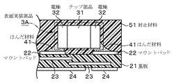
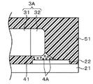
図2は、上記実施形態において作成された、電子部品内部の表面実装部品3Aを示す拡大図である。図3は、表面実装部品3Aの電極32とマウントパッド21との接合部を示した拡大図であり、はんだ材料41中には金属粉4Aが分散されている様子を模式的に示している。図4は、前記はんだ材料41中における金属粉4Aの様子を示した説明図である。本実施形態については、前述のように、はんだ材料41中に含まれるはんだ粉末として例えば、Sn−3・0Ag−0.5Cuはんだを用いている。また、はんだ材料41中に含まれる金属粉4Aは、例えばCuよりなる本体部43及び本体部43表面にメッキされた例えばAgよりなる金属膜42により構成されている。
FIG. 2 is an enlarged view showing the surface mounted
このような電子部品によれば、アプリケーション機器である電子機器例えば携帯電話の配線基板にはんだ付けするために電子部品を加熱した場合電子部品の封止材料内のはんだ材料が溶融しても体積膨張が抑えられるので、表面実装部品及び配線基板と封止材料との間の界面へのはんだ材料の侵入の程度が小さくなるので、故障を引き起こすおそれが小さくなる。なお電子機器をリペアーするために電子部品を配線基板から取り外す場合でも同様な効果が得られる。 According to such an electronic component, when the electronic component is heated to be soldered to an electronic device that is an application device, for example, a wiring board of a mobile phone, the volume expansion even if the solder material in the sealing material of the electronic component is melted Since the degree of penetration of the solder material into the interface between the surface mount component and the wiring board and the sealing material is reduced, the possibility of causing a failure is reduced. The same effect can be obtained even when the electronic component is removed from the wiring board in order to repair the electronic device.
ところで、本実施形態においては、はんだ材料41を構成するはんだ粉末をリフローにより溶融させる際に、金属膜42を構成するAgの一部あるいは総てが溶融されるようにリフローの温度プロファイルを設定してもよい。このようにすれば既述のように溶融したはんだ粉末と溶融した金属膜42を構成したAgが互いに混ざり合うため、前記はんだ組成物に比べて高い溶融温度をもつことになる。そのためはんだ材料41の体積膨張がさらに低下する好ましい効果が得られる。
By the way, in this embodiment, when melting the solder powder constituting the
21 基板
22 マウントパッド
3A 表面実装部品
3B 表面実装部品
31 チップ部品
32 電極
33 SAWチップ
36 インターポーザー
4A 金属粉
41 はんだ材料
42 金属膜
43 本体部
51 封止材料
52 メタルマスク
61 スキージ
21
Claims (5)
少なくともその内部が前記はんだ組成物の固相線温度よりも高い固相線温度を有する金属からなる金属粉と、
を混合してなり、
前記はんだ組成物は、当該はんだ組成物全体の質量に対してAgを2.0〜4.0質量%、Cuを0.1〜1.5質量%夫々含み、当該はんだ組成物の残部はSnにより構成され、
前記金属粉は、Cuからなる本体部と、本体部の表面を覆うAgからなる金属膜と、により構成され、前記はんだ組成物の質量に対して20〜35質量%混入されていることを特徴とするはんだ材料。 A solder composition based on Sn;
A metal powder made of a metal having at least a solidus temperature higher than the solidus temperature of the solder composition;
Mixed
The solder composition contains 2.0 to 4.0% by mass of Ag and 0.1 to 1.5% by mass of Cu with respect to the total mass of the solder composition, and the remainder of the solder composition is Sn. Composed of
The metal powder is composed of a main body portion made of Cu and a metal film made of Ag covering the surface of the main body portion, and 20 to 35 mass% is mixed with respect to the mass of the solder composition. Solder material.
このはんだ材料の上に表面実装部品を載せる工程と、
前記はんだ材料を加熱して溶融することにより表面実装部品の電極と配線基板の電極とを電気的に接続する工程と、
前記表面実装部品を封止材料により封止する工程と、
を含むことを特徴とする電子部品の製造方法。 Supplying the solder material according to claim 1 or 2 onto an electrode of a wiring board;
A process of placing a surface mount component on the solder material;
Electrically connecting the electrodes of the surface mount component and the electrodes of the wiring board by heating and melting the solder material;
Sealing the surface-mounted component with a sealing material;
The manufacturing method of the electronic component characterized by including.
Priority Applications (1)
| Application Number | Priority Date | Filing Date | Title |
|---|---|---|---|
| JP2004291979A JP4435663B2 (en) | 2004-10-04 | 2004-10-04 | Solder material, electronic component, and method of manufacturing electronic component |
Applications Claiming Priority (1)
| Application Number | Priority Date | Filing Date | Title |
|---|---|---|---|
| JP2004291979A JP4435663B2 (en) | 2004-10-04 | 2004-10-04 | Solder material, electronic component, and method of manufacturing electronic component |
Publications (3)
| Publication Number | Publication Date |
|---|---|
| JP2006102769A JP2006102769A (en) | 2006-04-20 |
| JP2006102769A5 JP2006102769A5 (en) | 2009-08-06 |
| JP4435663B2 true JP4435663B2 (en) | 2010-03-24 |
Family
ID=36373061
Family Applications (1)
| Application Number | Title | Priority Date | Filing Date |
|---|---|---|---|
| JP2004291979A Expired - Fee Related JP4435663B2 (en) | 2004-10-04 | 2004-10-04 | Solder material, electronic component, and method of manufacturing electronic component |
Country Status (1)
| Country | Link |
|---|---|
| JP (1) | JP4435663B2 (en) |
Families Citing this family (4)
| Publication number | Priority date | Publication date | Assignee | Title |
|---|---|---|---|---|
| JP2012174332A (en) | 2011-02-17 | 2012-09-10 | Fujitsu Ltd | Conductive jointing material, method of jointing conductor, and method of manufacturing semiconductor |
| JP2013119089A (en) * | 2011-12-06 | 2013-06-17 | Fujitsu Ltd | Conductive bonding material, electronic component, and electronic device |
| KR102156373B1 (en) * | 2013-05-10 | 2020-09-16 | 엘지이노텍 주식회사 | Solder paste |
| CN114055008B (en) * | 2021-11-18 | 2023-09-05 | 陕西众森电能科技有限公司 | Metal powder for preparing superfine soldering paste, soldering paste and preparation method thereof |
-
2004
- 2004-10-04 JP JP2004291979A patent/JP4435663B2/en not_active Expired - Fee Related
Also Published As
| Publication number | Publication date |
|---|---|
| JP2006102769A (en) | 2006-04-20 |
Similar Documents
| Publication | Publication Date | Title |
|---|---|---|
| JP3476464B2 (en) | Tin-bismuth solder paste and a method for forming a connection with improved high-temperature characteristics using the paste | |
| JP4633630B2 (en) | Soldering flux and soldering method | |
| JP5045673B2 (en) | Functional component lid and manufacturing method thereof | |
| KR100776114B1 (en) | Paste for soldering and soldering method using the same | |
| US6360939B1 (en) | Lead-free electrical solder and method of manufacturing | |
| US5452842A (en) | Tin-zinc solder connection to a printed circuit board or the like | |
| EP1946626B1 (en) | Method for soldering electronic component and soldering structure of electronic component | |
| JP2008510620A (en) | Solder composition, solder joint method, and solder joint structure | |
| JP4356581B2 (en) | Electronic component mounting method | |
| WO2010098357A1 (en) | Metal filler, low-temperature-bonding lead-free solder and bonded structure | |
| JP4063271B2 (en) | Solder paste and soldering method | |
| JP2011147982A (en) | Solder, electronic component, and method for manufacturing the electronic component | |
| JP5453385B2 (en) | Solder paste | |
| JP2004274000A (en) | Soldering method | |
| JP4435663B2 (en) | Solder material, electronic component, and method of manufacturing electronic component | |
| JP4471825B2 (en) | Electronic component and method for manufacturing electronic component | |
| JP2008006499A (en) | Solder paste | |
| JP4134976B2 (en) | Solder bonding method | |
| JP2008238253A (en) | Pb-FREE SOLDERING MATERIAL, AND MANUFACTURING METHOD OF SEMI-CONDUCTOR MOUNTED STRUCTURE USING THE SAME | |
| JP5724088B2 (en) | Metal filler and lead-free solder containing the same | |
| JP5652689B2 (en) | Manufacturing method of electronic component bonded structure and electronic component bonded structure obtained by the manufacturing method | |
| JP4259431B2 (en) | Solder paste and solder joining method | |
| JPH0417994A (en) | Solder composition | |
| JP2004095907A (en) | Solder joint structure and solder paste | |
| JP2004001030A (en) | Soldering paste and method for manufacturing semiconductor device |
Legal Events
| Date | Code | Title | Description |
|---|---|---|---|
| A621 | Written request for application examination |
Free format text: JAPANESE INTERMEDIATE CODE: A621 Effective date: 20070823 |
|
| A521 | Written amendment |
Free format text: JAPANESE INTERMEDIATE CODE: A523 Effective date: 20090624 |
|
| A871 | Explanation of circumstances concerning accelerated examination |
Free format text: JAPANESE INTERMEDIATE CODE: A871 Effective date: 20090624 |
|
| A975 | Report on accelerated examination |
Free format text: JAPANESE INTERMEDIATE CODE: A971005 Effective date: 20090710 |
|
| A131 | Notification of reasons for refusal |
Free format text: JAPANESE INTERMEDIATE CODE: A131 Effective date: 20090811 |
|
| A521 | Written amendment |
Free format text: JAPANESE INTERMEDIATE CODE: A523 Effective date: 20091013 |
|
| TRDD | Decision of grant or rejection written | ||
| A01 | Written decision to grant a patent or to grant a registration (utility model) |
Free format text: JAPANESE INTERMEDIATE CODE: A01 Effective date: 20091215 |
|
| A01 | Written decision to grant a patent or to grant a registration (utility model) |
Free format text: JAPANESE INTERMEDIATE CODE: A01 |
|
| A61 | First payment of annual fees (during grant procedure) |
Free format text: JAPANESE INTERMEDIATE CODE: A61 Effective date: 20091224 |
|
| R150 | Certificate of patent or registration of utility model |
Ref document number: 4435663 Country of ref document: JP Free format text: JAPANESE INTERMEDIATE CODE: R150 Free format text: JAPANESE INTERMEDIATE CODE: R150 |
|
| FPAY | Renewal fee payment (event date is renewal date of database) |
Free format text: PAYMENT UNTIL: 20130108 Year of fee payment: 3 |
|
| FPAY | Renewal fee payment (event date is renewal date of database) |
Free format text: PAYMENT UNTIL: 20130108 Year of fee payment: 3 |
|
| FPAY | Renewal fee payment (event date is renewal date of database) |
Free format text: PAYMENT UNTIL: 20130108 Year of fee payment: 3 |
|
| FPAY | Renewal fee payment (event date is renewal date of database) |
Free format text: PAYMENT UNTIL: 20140108 Year of fee payment: 4 |
|
| R250 | Receipt of annual fees |
Free format text: JAPANESE INTERMEDIATE CODE: R250 |
|
| R250 | Receipt of annual fees |
Free format text: JAPANESE INTERMEDIATE CODE: R250 |
|
| R250 | Receipt of annual fees |
Free format text: JAPANESE INTERMEDIATE CODE: R250 |
|
| R250 | Receipt of annual fees |
Free format text: JAPANESE INTERMEDIATE CODE: R250 |
|
| R250 | Receipt of annual fees |
Free format text: JAPANESE INTERMEDIATE CODE: R250 |
|
| R250 | Receipt of annual fees |
Free format text: JAPANESE INTERMEDIATE CODE: R250 |
|
| R250 | Receipt of annual fees |
Free format text: JAPANESE INTERMEDIATE CODE: R250 |
|
| LAPS | Cancellation because of no payment of annual fees |