JP4433763B2 - Field device memory update method and system - Google Patents
Field device memory update method and system Download PDFInfo
- Publication number
- JP4433763B2 JP4433763B2 JP2003371648A JP2003371648A JP4433763B2 JP 4433763 B2 JP4433763 B2 JP 4433763B2 JP 2003371648 A JP2003371648 A JP 2003371648A JP 2003371648 A JP2003371648 A JP 2003371648A JP 4433763 B2 JP4433763 B2 JP 4433763B2
- Authority
- JP
- Japan
- Prior art keywords
- update
- field
- memory
- field device
- host system
- Prior art date
- Legal status (The legal status is an assumption and is not a legal conclusion. Google has not performed a legal analysis and makes no representation as to the accuracy of the status listed.)
- Expired - Lifetime
Links
- 238000000034 method Methods 0.000 title claims description 19
- 238000012546 transfer Methods 0.000 claims description 8
- 230000009191 jumping Effects 0.000 claims description 5
- 238000012544 monitoring process Methods 0.000 claims description 5
- 238000004891 communication Methods 0.000 description 5
- 230000000694 effects Effects 0.000 description 5
- 230000006870 function Effects 0.000 description 5
- 238000004886 process control Methods 0.000 description 4
- 238000010586 diagram Methods 0.000 description 3
- 230000005540 biological transmission Effects 0.000 description 2
- 238000004364 calculation method Methods 0.000 description 1
- 238000006243 chemical reaction Methods 0.000 description 1
- 238000013461 design Methods 0.000 description 1
- 238000012905 input function Methods 0.000 description 1
- 238000005259 measurement Methods 0.000 description 1
- 238000004092 self-diagnosis Methods 0.000 description 1
Images
Description
本発明は、プロセス現場で使用されるフィールド機器内の不揮発性メモリに格納されているファームウエアあるいはコンフィギュレーション情報などのデータを書き替える方法およびそのシステムに関するものである。 The present invention relates to a method and system for rewriting data such as firmware or configuration information stored in a nonvolatile memory in a field device used in a process field.
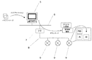
図3にプロセス制御システムの構成を示す。FOUNDATIONfieldbusやシリアル伝送などのフィールドバス8には複数のフィールド機器9が接続されている。これらフィールド機器9にはアナログインプットファンクションブロックAI、あるいはPIDファンクションブロックPID等が内蔵されている。
FIG. 3 shows the configuration of the process control system. A plurality of
フィールドバス8はIOユニット7、バス6を介してホストシステム5に接続されている。このようなプロセス制御システムにおいて、センサからの信号を入力し、フィールド機器9相互間あるいはフィールド機器9とホストシステム5との間でデータのやりとりをして制御を実行していく。
The
このようなフィールド機器では、センサからの信号を出力信号に変換するための演算部分のプログラムやネットワーク情報を構成するコンフィギュレーション情報は、通常EPROM、FlashROM、EEPROMなどの不揮発性メモリに保存されている。 In such a field device, the program of the calculation part for converting the signal from the sensor into the output signal and the configuration information constituting the network information are usually stored in a non-volatile memory such as EPROM, FlashROM, EEPROM or the like. .
近年、プロセスの改善等を目的とした機能分散を進める上で、フィールド機器9にも自己診断機能の拡張などの付加機能が求められるようになってきた。また、機能が豊富になったために、バグが発生する可能性も大きくなってきている。そのため、フィールドバス8の通信機能を用いてフィールド機器9内部のファームウエアを更新することも行われている。
In recent years, additional functions such as expansion of the self-diagnosis function have been required for the
このような場合、ホストシステム5にファームウエアのバイナリイメージを入力し、バス6、IOユニット7、フィールドバス8を介してこのバイナリイメージをフィールド機器9に伝送して書き換えを行う。ホストシステム5は、ウエブサイトからインターネットを経由してバイナリイメージを取得することもある。
In such a case, a binary image of firmware is input to the
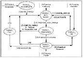
図4にFOUNDATIONFieldbusの仕様の一部を示す。この仕様はフィールドバス通信を介してフィールド機器9内部のファームウエアを更新することを想定しており、PREPARE_FOR_DWNLD、CANCEL_DWNLDなどの信号が用意されている。
Fig. 4 shows a part of the specifications of FOUNDATION Fieldbus. This specification assumes that the firmware in the
しかしながら、このようなフィールド機器では、ファームウエアを更新するためには次のような課題があった。 However, such field devices have the following problems in order to update the firmware.
不揮発性メモリとしてEPROMを使用しているフィールド機器では、新しいファームウエアが格納されたEEPROMと交換するか、フィールド機器自体を交換しなければならず、手間がかかるという課題があった。 A field device using an EPROM as a non-volatile memory has a problem that it is necessary to replace the EEPROM with new firmware or to replace the field device itself.
不揮発性メモリとしてFlashROMやEEPROMを使用しているフィールド機器では、フィールドバスを介してファームウエアの更新を行うことができる。しかし、更新時にはフィールド機器の消費電流が一時的に増加するという課題があった。 In a field device using FlashROM or EEPROM as a nonvolatile memory, firmware can be updated via a fieldbus. However, there has been a problem that current consumption of the field device temporarily increases at the time of update.
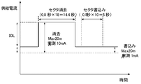
図5にFlashROMを書き替えるときの消費電流の実測値を示す。FlashROMを書き替えるときは、まずセクタ単位で消去した後、書き込みを行う。セクタ消去時の消費電流の増加量IDLは最大20mA、実測10mAであった。また、書き込み時の消費電流の増加は最大20mAであるが、実測では1mAであった。このことから、主としてセクタ消去時に消費電流が増加することがわかる。 FIG. 5 shows measured values of current consumption when the FlashROM is rewritten. When rewriting the flash ROM, the data is first erased in units of sectors and then written. The increase amount IDL of the current consumption at the time of sector erasing was 20 mA at maximum and 10 mA actually measured. The increase in current consumption during writing was 20 mA at maximum, but it was 1 mA in actual measurement. From this, it can be seen that the current consumption increases mainly during sector erasure.
このため、ホストシステム5が任意にフィールド機器9のファームウエアを書き替えるとすると、フィールド機器1台あたり20mAの消費電流の増加を見込んで電源などの設計を行わなければならず、コストが増大してしまうという課題があった。
For this reason, if the
ホストシステム5が1台ずつ順番にフィールド機器9のファームウエアを更新するとすると、消費電流は最大20mAに抑えることができる。しかしながら、更新のために30分/台程度の時間が必要であるために、セグメント内に10台のフィールド機器が接続されているとすると300分の時間が必要になり、実用的でないという課題もあった。
If the
例えば、差圧伝送器のファームウエアのサイズは約300kバイトである。通信間隔を1秒、通信間隔毎の転送バイト数を200バイトとすると、書き替えには
更新時間=ROM容量×通信間隔(秒)÷転送バイト数
=300k×1÷200=1500秒=25分
の更新時間が必要である。
For example, the size of the differential pressure transmitter firmware is about 300 kbytes. Assuming that the communication interval is 1 second and the number of transfer bytes per communication interval is 200 bytes, rewriting requires update time = ROM capacity × communication interval (seconds) / number of transfer bytes
= 300k × 1 ÷ 200 = 1500 seconds = 25 minutes of update time is required.
このため、フィールド機器9への供給電流が不足して書き替えることができず、またフィールドバス8に接続することができるフィールド機器9の台数が制限されてしまうという課題もあった。
For this reason, there is a problem that the current supplied to the
従って本発明が解決しようとする課題は、ファームウエア更新時の消費電流の増加を最小限に抑えることができ、かつ更新時間を短くすることができるフィールド機器のメモリ更新方法およびそのシステムを実現することにある。 Therefore, the problem to be solved by the present invention is to realize a memory update method and system for a field device that can minimize an increase in current consumption during firmware update and can shorten the update time. There is.
このような課題を達成する本発明は以下の通りである。
(1) フィールドバスに接続されたフィールド機器内部の不揮発性メモリに格納されたデータを前記フィールドバスに接続されたホストシステムが更新するフィールド機器のメモリ更新方法において、前記ホストシステムが、更新すべき前記フィールド機器の台数を取得する第1の工程と、前記ホストシステムが、更新が完了したフィールド機器の台数を表す更新完了台数を0にする第2の工程と、前記ホストシステムが、前記第1の工程で取得したフィールド機器の台数、および前記更新完了台数に基づいて全てのフィールド機器がメモリ更新を終了したかを判断し、全行程を終了する第3の工程と、前記ホストシステムが、前記フィールド機器のフラグを監視することにより、全ての前記フィールド機器がメモリを消去するメモリ更新の準備を完了するまで待機する第4の工程と、前記ホストシステムは前記第4の工程が終了すると、指定されたフィールド機器に更新命令を送信し、かつ更新データの転送を開始する第5の工程と、前記ホストシステムは、前記第5の工程が終了した後更新命令を送信するフィールド機器の指定を変更し、同一セグメント内の前記フィールド機器どれかが、データの書き込みを行うメモリ更新を完了すると、前記更新完了台数を1増加させて前記第3の工程にジャンプし、メモリ更新中であると前記更新完了台数を増加させないで前記第3の工程にジャンプする第6の工程と、
を有することを特徴とするフィールド機器のメモリ更新方法。
(2)フィールドバスと、不揮発性メモリが内蔵され、前記フィールドバスに接続されて
ステータス情報を前記フィールドバスに出力する複数のフィールド機器と、前記フィール
ドバスに接続され、請求項1記載のフィールド機器のメモリ更新方法を実行するホストシステムと、を有することを特徴とするフィールド機器のメモリ更新システム。
また、本発明は、フィールドバスに接続されたフィールド機器内部の不揮発性メモリに格納されたデータを更新するフィールド機器のメモリ更新方法において、前記不揮発性メモリを更新すべきフィールド機器の台数を含めたフィールド機器の情報を取得する第1の工程と、更新完了台数を
にする第2の工程と、全てのフィールド機器がメモリ更新を終了したかを判断し、メモリ更新を終了する第3の工程と、前記不揮発性メモリを更新すべき全てのフィールド機器がメモリ更新の準備中でなくなるまで待機する第4の工程と、前記第4の工程が終了すると、指定されたフィールド機器に更新命令を送信し、かつ更新データの転送を開始する第5の工程と、前記第4の工程が終了した後更新命令を送信するフィールド機器の指定を変更し、同一セグメント内の前記フィールド機器どれかが、データの書き込みを行うメモリ更新を終了すると、前記更新完了台数を1増加させて前記第3の工程にジャンプし、メモリ更新中であると前記更新完了台数を増加させないで前記第3の工程にジャンプする第6の工程とを具備するようにしたものである。
The present invention which achieves such a problem is as follows.
(1) In a memory update method for a field device in which data stored in a nonvolatile memory inside a field device connected to a field bus is updated by a host system connected to the field bus, the host system should update A first step of obtaining the number of field devices, a second step of setting the number of update completions indicating the number of field devices for which the host system has been updated to 0, and the host system including the first step determining whether all of the field device has finished the memory updated based field number of equipment obtained in step, and the update completion number, a third step of terminating the entire process, the host system, the By monitoring the field device flag, all the field devices erase the memory. A fourth step of waiting until the ready, the the host system the fourth step is completed, the fifth step to start sending the update command for the specified field device, and update the data transfer The host system changes the designation of the field device to which the update command is transmitted after the fifth step is completed, and when any of the field devices in the same segment completes the memory update for writing data. A sixth step of jumping to the third step by incrementing the update completion number by 1 and jumping to the third step without increasing the number of update completions when the memory is being updated;
Memory update methods of the field device, characterized in that it comprises a.
(2) The field device according to
The present invention also includes a field device memory update method for updating data stored in a nonvolatile memory inside a field device connected to a field bus, including the number of field devices to which the nonvolatile memory is to be updated. The first step to acquire field device information and the number of completed updates
A second step of determining whether all field devices have completed the memory update, a third step of ending the memory update, and all field devices to which the nonvolatile memory is to be updated a fourth step of waiting until no being prepared, when the fourth step is completed, a fifth step of starting the sending of the update command for the specified field device, and update the data transfer, the first After the process of 4 is completed, the designation of the field device that transmits the update command is changed, and when any of the field devices in the same segment finishes the memory update for writing data, the update completion number is increased by 1. jumps to the third step Te, and so that and a sixth step of jumping to the third step without that the memory updating increasing the update completion number Than is.
さらに、本発明は、フィールドバスと、不揮発性メモリが内蔵され、前記フィールドバ
スに接続されて、ステータス情報を前記フィールドバスに出力する複数のフィールド機器
と、請求項1記載のフィールド機器のメモリ更新方法を実行するホストシステムとを具備したものである。メモリ更新時の消費電流の増加を抑えることができ、かつ更新時間を短縮できる。
Furthermore, the present invention provides a field bus, a non-volatile memory, a plurality of field devices connected to the field bus and outputting status information to the field bus, and a memory update of the field device according to
以上説明したことから明らかなように、本発明によれば次のような効果がある。
請求項1の発明によれば、不揮発性メモリを更新すべきフィールド機器を監視して、更新すべきフィールド機器の全てがメモリ更新の準備中でないときに、更新すべきフィールド機器の1つに更新命令を送信し、更新データの転送を開始するようにした。
As is apparent from the above description, the present invention has the following effects.
According to the first aspect of the present invention, the field device to be updated in the nonvolatile memory is monitored, and when all the field devices to be updated are not in preparation for the memory update, the field device is updated to one of the field devices to be updated An instruction was sent to start the transfer of update data.
メモリ更新の準備中には、消費電力が大きいメモリ消去が行われる。この発明は全てのフィールド機器がメモリ更新の準備中でない場合にのみ更新命令を送信する。そのため、
1度に1台のフィード機器しかメモリ消去を行わないので、消費電流の増加を最小限に抑えることができるという効果がある。そのため、メモリ更新時に電流不足になることがなくなり、1つのセグメント内に接続できるフィールド機器の台数が制限されることもないという効果もある。また、短時間でメモリ更新を行うことができるという効果もある。
During memory update preparation, memory erasure with high power consumption is performed. The present invention transmits an update command only when all field devices are not preparing to update the memory. for that reason,
Since only one feed device at a time erases memory, an increase in current consumption can be minimized. Therefore, there is no current shortage when updating the memory, and there is an effect that the number of field devices that can be connected in one segment is not limited. In addition, there is an effect that the memory can be updated in a short time.
請求項2の発明によれば、フィールドバスと、このフィールドバスに接続された複数のフィールド機器および前記フィールドバスに接続されたホストシステムから構成されるシステムであって、このホストシステムは不揮発性メモリを更新すべきフィールド機器を監視して、更新すべきフィールド機器の全てがメモリ更新の準備中でないときに、更新すべきフィールド機器の1つに更新命令を送信し、更新データの転送を開始するようにした。
According to the invention of
1度に1台のフィード機器しか消費電力の大きいメモリ消去を行わないので、消費電流の増加を最小限に抑えることができるという効果がある。そのため、メモリ更新時に電流不足になることがなくなり、1つのセグメント内に接続できるフィールド機器の台数が制限されることもないという効果もある。また、短時間でメモリ更新を行うことができるという効果もある。 Since only one feed device at a time erases memory with high power consumption, an increase in current consumption can be minimized. Therefore, there is no current shortage when updating the memory, and there is an effect that the number of field devices that can be connected in one segment is not limited. Further, there is an effect that the memory can be updated in a short time.
以下本発明を図面を用いて詳細に説明する。プロセス制御システムの構成は図3と同じなので、説明を省略する。フィールド機器9はシステムの構成に応じてセグメントに分割され管理されている。1つのセグメントには複数のフィールド機器9が含まれている。また、フィールド機器9内部の不揮発性メモリの内容を更新するときは、このセグメントを単位として行われる。
Hereinafter, the present invention will be described in detail with reference to the drawings. The configuration of the process control system is the same as that in FIG. The
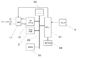
図1は本発明に係るフィールド機器の一実施例を示す構成図である。図1において、11はMAU(Media Attachment Unit)であり、図示しないフィールドバスに接続される。このMAU11はデジタル信号とアナログ信号の相互変換、データの衝突の監視などを行う。また、電流制御回路としての働きもある。
FIG. 1 is a block diagram showing an embodiment of a field device according to the present invention. In FIG. 1, 11 is a MAU (Media Attachment Unit), which is connected to a field bus (not shown). The
12はFBモデムであり、信号をフィールドバスに出力する形式に変換し、フィールドバス上の信号を逆変換する。Txはフィールドバスに出力する信号、Rxはフィールドバスから入力する信号である。
2はFlashROMであり、ファームウエアやコンフィギュレーション情報などのデータが格納される。31はCPUであり、このフィールド機器全体の制御を行う。32はSRAMであり、CPU31の作業領域などに使用される。
A
33はゲートアレイであり、必要なデジタル回路が格納されている。34はEEPROMであり、CPU31が使用するパラメータなどが保管される。CPU31,SRAM32,ゲートアレイ33、FBモデム12およびFlashROM2はバス35で相互に接続されている。4はプロセス量を測定するセンサであり、その出力はCPU31に入力される。
CPU31はFlashROM2に内蔵されているプログラムに従ってセンサ4の出力およびフィールドバス上のデータを取りこんで制御出力を演算し、フィールドバスに出力する。
The
前述したように、FlashROMやEEPROM等の不揮発性メモリでは、メモリの内容を書き換える前に消去しなければならない。フィールド機器が更新命令を受信するとメモリ更新の準備中に移行し、その内部の不揮発性メモリの内容を消去する。このときはDWNLD_PREPARINIGフラグがオンになる。すなわち、DWNLD_PREPARINIGフラグを監視することにより、メモリが消去中であるかどうかを判断することができる。 As described above, in a non-volatile memory such as FlashROM or EEPROM, the contents of the memory must be erased before rewriting. When the field device receives the update command, it shifts to the preparation of the memory update and erases the contents of the internal nonvolatile memory. At this time, the DWNLD_PREPARINIG flag is turned on. That is, by monitoring the DWNLD_PREPARINIG flag, it can be determined whether or not the memory is being erased.
このため、DWNLD_PREPARINIGフラグを監視して、フィールド機器の1つがメモリ更新の準備中のときは他のフィールド機器に更新命令を送信しないようにすることにより、2つ以上のフィールド機器が消費電力の大きい消去動作を同時に行うことを避けることができる。 Therefore, by monitoring the DWNLD_PREPARINIG flag so that when one of the field devices is preparing to update the memory, the update command is not transmitted to the other field devices, so that two or more field devices have high power consumption. It is possible to avoid performing the erase operation simultaneously.
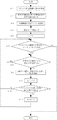
図2にFlashROM2を更新するときのフローチャートを示す。最初にA−1でセグメント内の全機種の情報、例えば製造業者、対象機種、ノードアドレス、タグ、レビジョンを取得する。これはプログラムの起動時でもよく、あるいは事前に何らかの方法で取得してもよい。
FIG. 2 shows a flowchart when the
次に、A−2でファームウエアを更新する機種の情報を取得する。この情報にはメモリを更新を行うフィールド機器の台数が含まれ、この台数をNとする。次に、A−3で更新するバイナリイメージが格納されているファイルを選択する。 Next, in A-2, information on the model whose firmware is to be updated is acquired. This information includes the number of field devices that update the memory, and this number is N. Next, a file storing a binary image to be updated in A-3 is selected.
次に、A−4で更新完了台数mを0とし、A−5でnを1とする。そして、A−6でセグメント内の全フィールド機器の更新が終了したかどうかを判定する。これは、更新完了台数mが更新機器台数Nよりも1小さい値になったかどうかで判定する。 Next, the update completion number m is set to 0 in A-4, and n is set to 1 in A-5. Then, in A-6, it is determined whether or not the update of all field devices in the segment is completed. This is determined based on whether or not the update completion number m has become a value smaller than the update device number N by one.
次に、A−7でメモリ更新する全てのフィールド機器が更新作業の準備中でないかどうかを判定する。どれかのフィールド機器が準備中のときはこのA−7の入り口に戻るので、メモリ更新する全てのフィールド機器が更新準備を完了するまで、このA−7で待機することになる。 Next, in A-7, it is determined whether or not all field devices to be updated in memory are not preparing for the update operation. When any field device is in preparation, the process returns to the entrance of A-7, so that all the field devices to be updated in memory wait at A-7 until completion of preparation for update.
メモリ更新する全フィールド機器がメモリ更新の準備中でなくなると、A−8でn番目のフィールド機器に更新命令を送信し、続いて更新するデータの送信を開始する。そして、A−9でnに1を加算する。 When all the field devices to update the memory are not ready for the memory update, an update command is transmitted to the n-th field device at A-8, and then transmission of data to be updated is started. Then, 1 is added to n in A-9.
そして、A−10でセグメント内の任意のフィールド機器に対する更新が終了した、すなわちセグメント内の全てのフィールド機器が更新中でないと更新完了台数mに1を加算してA−6の先頭に戻り、セグメント内のどれかのフィールド機器が更新中であると、なにもしないでA−6の先頭に戻る。 Then, the update for any field device in the segment is completed in A-10, that is, if all the field devices in the segment are not being updated, 1 is added to the update completion number m and the process returns to the beginning of A-6. If any field device in the segment is being updated, it returns to the top of A-6 without doing anything.
すなわち、A−7でメモリ更新すべき全フィールド機器がメモリ更新の準備ができていることを確認してから、順番にフィールド機器に更新命令を送信して、更新データの転送を開始するようにする。そのため、1度に1台のフィード機器しかメモリ更新を行わないので、消費電流の増加を最小限に抑えることができる。 That is, after confirming that all field devices to be updated in A-7 are ready for the memory update in A-7, an update command is sequentially transmitted to the field devices to start transfer of update data. To do. As a result, only one feed device is updated at a time, so that an increase in current consumption can be minimized.
また、消費電力の増加が少ない書き込みは並行して行うようにするので、メモリの更新時間を大幅に短縮することができる。FlashROMの全セクタを消去するのに15〜30秒必要なので、例えば、セグメント内に10台のフィールド機器が接続されている場合は、
更新時間=FlashROM2のデータ消去時間×接続台数+1台当たりの更新時間
=15秒×10+30分=32.5分
となり、1台ずつ更新した場合の約1/10の時間で更新作業を行うことができる。
In addition, since writing with little increase in power consumption is performed in parallel, the memory update time can be greatly shortened. Since it takes 15 to 30 seconds to erase all the sectors of the FlashROM, for example, when 10 field devices are connected in the segment,
Update time = FlashROM2 data erase time x Number of connected devices + Update time per unit
= 15 seconds × 10 + 30 minutes = 32.5 minutes, and the update work can be performed in about 1/10 of the time when each unit is updated.
11 MAU
12 FBモデム
2 FlashROM
31 CPU
5 ホストシステム
8 フィールドバス
9 フィールド機器
11 MAU
12
31 CPU
5
Claims (2)
前記ホストシステムが、不揮発性メモリの内容を更新する単位であるセグメント内の更新すべき前記フィールド機器の台数を取得する第1の工程と、
前記ホストシステムが、更新が完了したフィールド機器の台数を表す更新完了台数を0にすると共に、更新命令を送信するフィールド機器を指定する番号を初期化する第2の工程と、
前記ホストシステムが、前記第1の工程で取得したフィールド機器の台数、および前記更新完了台数に基づいて全てのフィールド機器がメモリ更新を終了したかを判断し、終了したと判断するとメモリ更新を終了する第3の工程と、
前記ホストシステムが、前記フィールド機器のフラグを監視することにより、前記フィールド機器のうち、メモリを消去するメモリ更新の準備中のフィールド機器がなくなるまで待機する第4の工程と、
前記ホストシステムは、前記第4の工程が終了すると、前記更新命令を送信するフィールド機器を指定する番号で指定されたフィールド機器に更新命令を送信して更新の準備を開始させ、かつ更新データの転送を開始する第5の工程と、
前記ホストシステムは、前記第5の工程が終了した後更新命令を送信するフィールド機器を指定する番号を変更し、前記セグメントの同じセグメント内の前記フィールド機器のどれかがメモリ更新を終了すると、前記更新完了台数を1増加させて前記第3の工程にジャンプし、メモリ更新中であると前記更新完了台数を増加させないで前記第3の工程にジャンプする第6の工程と、
を有することを特徴とするフィールド機器のメモリ更新方法。 In a memory update method for a field device in which a host system connected to the field bus updates data stored in a nonvolatile memory inside the field device connected to the field bus.
A first step in which the host system acquires the number of field devices to be updated in a segment, which is a unit for updating the contents of a nonvolatile memory ;
A second step in which the host system sets the number of update completions indicating the number of field devices that have been updated to 0, and initializes a number that specifies a field device that transmits an update command ;
Exit the host system, said first number of field devices obtained in step, and wherein all field device based on the updated completion number is determined whether to exit the memory update, the memory update if it is determined to have been completed A third step of
A fourth step in which the host system waits until there is no field device in preparation for memory update for erasing the memory , by monitoring the flag of the field device ;
Upon completion of the fourth step, the host system sends an update command to the field device designated by the number designating the field device to which the update command is sent, starts update preparation, and updates data A fifth step of starting the transfer;
The host system changes a number specifying a field device to which an update command is transmitted after the fifth step is finished, and when any of the field devices in the same segment of the segment finishes the memory update, A sixth step of jumping to the third step by increasing the number of update completions by 1 and jumping to the third step without increasing the number of update completions when the memory is being updated; and
A memory update method for a field device, comprising:
不揮発性メモリが内蔵され、前記フィールドバスに接続されてステータス情報を前記フィールドバスに出力する複数のフィールド機器と、
前記フィールドバスに接続され、請求項1記載のフィールド機器のメモリ更新方法を実行するホストシステムと、を有することを特徴とするフィールド機器のメモリ更新システム。 With fieldbus,
A plurality of field devices that have built-in nonvolatile memory and are connected to the field bus and output status information to the field bus;
A memory update system for a field device, comprising: a host system connected to the field bus and executing the memory update method for a field device according to claim 1.
Priority Applications (1)
| Application Number | Priority Date | Filing Date | Title |
|---|---|---|---|
| JP2003371648A JP4433763B2 (en) | 2003-10-31 | 2003-10-31 | Field device memory update method and system |
Applications Claiming Priority (1)
| Application Number | Priority Date | Filing Date | Title |
|---|---|---|---|
| JP2003371648A JP4433763B2 (en) | 2003-10-31 | 2003-10-31 | Field device memory update method and system |
Publications (3)
| Publication Number | Publication Date |
|---|---|
| JP2005135223A JP2005135223A (en) | 2005-05-26 |
| JP2005135223A5 JP2005135223A5 (en) | 2006-09-14 |
| JP4433763B2 true JP4433763B2 (en) | 2010-03-17 |
Family
ID=34648237
Family Applications (1)
| Application Number | Title | Priority Date | Filing Date |
|---|---|---|---|
| JP2003371648A Expired - Lifetime JP4433763B2 (en) | 2003-10-31 | 2003-10-31 | Field device memory update method and system |
Country Status (1)
| Country | Link |
|---|---|
| JP (1) | JP4433763B2 (en) |
Families Citing this family (4)
| Publication number | Priority date | Publication date | Assignee | Title |
|---|---|---|---|---|
| JP4411953B2 (en) * | 2003-12-09 | 2010-02-10 | 横河電機株式会社 | Memory update system for field devices |
| US7698242B2 (en) * | 2006-08-16 | 2010-04-13 | Fisher-Rosemount Systems, Inc. | Systems and methods to maintain process control systems using information retrieved from a database storing general-type information and specific-type information |
| JP2012038056A (en) * | 2010-08-06 | 2012-02-23 | Yokogawa Electric Corp | Method and system for updating memory content of equipment connected to communication bus |
| JP2012043127A (en) * | 2010-08-18 | 2012-03-01 | Yokogawa Electric Corp | Field instrument |
Family Cites Families (6)
| Publication number | Priority date | Publication date | Assignee | Title |
|---|---|---|---|---|
| JP2581001B2 (en) * | 1994-04-26 | 1997-02-12 | 日本電気株式会社 | Information management apparatus and information management method |
| JPH10105409A (en) * | 1996-10-02 | 1998-04-24 | Sharp Corp | Slave module managing system for device |
| JP3837201B2 (en) * | 1997-02-27 | 2006-10-25 | 三洋電機株式会社 | Flash memory CPU type control device and device using the same |
| JP3626328B2 (en) * | 1997-07-24 | 2005-03-09 | 三菱電機株式会社 | Vehicle control device |
| US6850973B1 (en) * | 1999-09-29 | 2005-02-01 | Fisher-Rosemount Systems, Inc. | Downloadable code in a distributed process control system |
| DE10155189A1 (en) * | 2001-11-12 | 2003-07-03 | Endress & Hauser Gmbh & Co Kg | Method for controlling the power supply of several field devices |
-
2003
- 2003-10-31 JP JP2003371648A patent/JP4433763B2/en not_active Expired - Lifetime
Also Published As
| Publication number | Publication date |
|---|---|
| JP2005135223A (en) | 2005-05-26 |
Similar Documents
| Publication | Publication Date | Title |
|---|---|---|
| JP4411953B2 (en) | Memory update system for field devices | |
| CN100446126C (en) | Flash memory access using a plurality of command cycles | |
| EP0991081B1 (en) | Emulated EEPROM memory device and corresponding method | |
| CN102331943B (en) | System and method for updating storage on line | |
| CN104951334B (en) | FPGA biplate QSPI flash program loading method | |
| US20150227128A1 (en) | Control device and communication control method | |
| US20050144366A1 (en) | Data management apparatus and method, non-volatile memory, storage device having the non-volatile memory and data processing system | |
| WO2018054060A1 (en) | Processor and bootloader program update method, and storage medium | |
| JP2014126989A (en) | Control device, control method, and program | |
| US8036786B2 (en) | On-vehicle control apparatus | |
| JP4433763B2 (en) | Field device memory update method and system | |
| KR100746036B1 (en) | Apparatus and method for controlling flash memory | |
| JP2012093961A (en) | Control apparatus and method, and program write system | |
| JP2001134629A (en) | Simulation method and simulation system | |
| CN104881338B (en) | Semiconductor equipment | |
| JP2004021867A (en) | Information processing system | |
| JP2007114943A (en) | Method of updating firmware and information processing apparatus | |
| JP2011108161A (en) | Information processor | |
| CN111007989A (en) | Storage and use method of missile-borne FLASH chip bad block information | |
| JP2009080736A (en) | Plc construction method | |
| JP2005151453A (en) | Method for managing constituent element data | |
| JP2006031405A (en) | Memory update method for field equipment | |
| JP2008257415A (en) | Controller having program write function | |
| JP2019020837A (en) | Electronic controller | |
| JP2005141457A (en) | Program updating system |
Legal Events
| Date | Code | Title | Description |
|---|---|---|---|
| A521 | Request for written amendment filed |
Free format text: JAPANESE INTERMEDIATE CODE: A523 Effective date: 20060802 |
|
| A621 | Written request for application examination |
Free format text: JAPANESE INTERMEDIATE CODE: A621 Effective date: 20060802 |
|
| A977 | Report on retrieval |
Free format text: JAPANESE INTERMEDIATE CODE: A971007 Effective date: 20090115 |
|
| A131 | Notification of reasons for refusal |
Free format text: JAPANESE INTERMEDIATE CODE: A131 Effective date: 20090708 |
|
| A521 | Request for written amendment filed |
Free format text: JAPANESE INTERMEDIATE CODE: A523 Effective date: 20090825 |
|
| A131 | Notification of reasons for refusal |
Free format text: JAPANESE INTERMEDIATE CODE: A131 Effective date: 20090917 |
|
| A521 | Request for written amendment filed |
Free format text: JAPANESE INTERMEDIATE CODE: A523 Effective date: 20091105 |
|
| TRDD | Decision of grant or rejection written | ||
| A01 | Written decision to grant a patent or to grant a registration (utility model) |
Free format text: JAPANESE INTERMEDIATE CODE: A01 Effective date: 20091208 |
|
| A01 | Written decision to grant a patent or to grant a registration (utility model) |
Free format text: JAPANESE INTERMEDIATE CODE: A01 |
|
| A61 | First payment of annual fees (during grant procedure) |
Free format text: JAPANESE INTERMEDIATE CODE: A61 Effective date: 20091221 |
|
| R150 | Certificate of patent or registration of utility model |
Ref document number: 4433763 Country of ref document: JP Free format text: JAPANESE INTERMEDIATE CODE: R150 Free format text: JAPANESE INTERMEDIATE CODE: R150 |
|
| FPAY | Renewal fee payment (event date is renewal date of database) |
Free format text: PAYMENT UNTIL: 20130108 Year of fee payment: 3 |
|
| FPAY | Renewal fee payment (event date is renewal date of database) |
Free format text: PAYMENT UNTIL: 20140108 Year of fee payment: 4 |
|
| EXPY | Cancellation because of completion of term |