JP4418713B2 - Random number generation method and random number generator - Google Patents
Random number generation method and random number generator Download PDFInfo
- Publication number
- JP4418713B2 JP4418713B2 JP2004174607A JP2004174607A JP4418713B2 JP 4418713 B2 JP4418713 B2 JP 4418713B2 JP 2004174607 A JP2004174607 A JP 2004174607A JP 2004174607 A JP2004174607 A JP 2004174607A JP 4418713 B2 JP4418713 B2 JP 4418713B2
- Authority
- JP
- Japan
- Prior art keywords
- bit
- bit string
- random number
- bits
- register
- Prior art date
- Legal status (The legal status is an assumption and is not a legal conclusion. Google has not performed a legal analysis and makes no representation as to the accuracy of the status listed.)
- Expired - Fee Related
Links
Images


Classifications
-
- G—PHYSICS
- G06—COMPUTING; CALCULATING OR COUNTING
- G06F—ELECTRIC DIGITAL DATA PROCESSING
- G06F7/00—Methods or arrangements for processing data by operating upon the order or content of the data handled
- G06F7/58—Random or pseudo-random number generators
- G06F7/582—Pseudo-random number generators
- G06F7/584—Pseudo-random number generators using finite field arithmetic, e.g. using a linear feedback shift register
-
- G—PHYSICS
- G06—COMPUTING; CALCULATING OR COUNTING
- G06F—ELECTRIC DIGITAL DATA PROCESSING
- G06F2207/00—Indexing scheme relating to methods or arrangements for processing data by operating upon the order or content of the data handled
- G06F2207/58—Indexing scheme relating to groups G06F7/58 - G06F7/588
- G06F2207/583—Serial finite field implementation, i.e. serial implementation of finite field arithmetic, generating one new bit or trit per step, e.g. using an LFSR or several independent LFSRs; also includes PRNGs with parallel operation between LFSR and outputs
Description
本発明は、乱数を発生させるための技術に関するものである。 The present invention relates to a technique for generating a random number.
論理演算を用いる乱数発生方法の一つとしてM系列というLビット長の乱数法がある。これは、xN=xN-K+xN-Lという式を用いるもので、用いる数字は0と1だけの1ビット乱数であり、Kを決めたとき特定のLに対して論理的な最上の周期をもつのでMaximum、LengthのMをとってM系列とよばれる。Kビットの内部状態(xN-K,xN-K+1,・・・、xN-1)が与えられればxN,xN+1以下一意的に値が決まるから、内部状態は2K通りである。上記の方程式の自明の解xn=0を除いて内部状態が2K−1個であり、M系列ではこれを周期とする。回路的には、シフトレジスタと、その途中の値をフィードバックするEXOR(排他的論理和)で構成され、実現する原始多項式に合わせて上記フィードバック構成が決定される。
上述したように、従来の乱数発生方法は、LFSR(Linear Feedback Shift Register)を用いているため、隣接する数値間に相関性があり、特有のスペクトラムを有している。特に、中・低域の周波数領域にピークがあり、画像処理等に用いる場合、画質妨害が問題となっていた。 As described above, since the conventional random number generation method uses LFSR (Linear Feedback Shift Register), there is a correlation between adjacent numerical values and a specific spectrum. In particular, there are peaks in the middle and low frequency regions, and image quality interference has been a problem when used for image processing and the like.
また、KビットのLFSRを用いた場合、周期は2K−1となり、1つの乱数発生器から複数周期の乱数を生成させることは困難であった。また、原始多項式も1つしか実現できなかったので、乱数のパターンも1つに限定されていた。 Further, when a K-bit LFSR is used, the cycle becomes 2 K −1, and it is difficult to generate a plurality of cycles of random numbers from one random number generator. Further, since only one primitive polynomial could be realized, the random number pattern was limited to one.
また、同じ乱数系列を逆方向に生成することも不可能であり、用途が限定されていた。 Further, it is impossible to generate the same random number sequence in the reverse direction, and the application is limited.
本発明は上述した課題を解決するためのものであり、Kビット以下の任意のM系列乱数を生成する為の技術を提供することを目的とする。 The present invention is for solving the above-described problems, and an object thereof is to provide a technique for generating an arbitrary M-sequence random number of K bits or less.
また本発明の別の目的としては、視覚的に良好な低域周波数成分の少ない乱数を生成することを目的とする。 Another object of the present invention is to generate a random number with a low frequency component that is visually good.
本発明の目的を達成するために、例えば本発明の乱数発生方法は以下の構成を備える。 In order to achieve the object of the present invention, for example, the random number generation method of the present invention comprises the following arrangement.
すなわち、Kビットで表現される乱数を発生する乱数発生方法であって、
マスクパターンを表すビットパターンを生成して設定する設定工程と、
メモリに保持されているKビットのビット列を前記ビットパターンでマスクするマスク工程と、
前記マスク工程でマスクしたビット列に対する排他的論理和演算を行い、当該排他的論理和演算結果を示すビット値を、前記メモリに保持されているKビットのビット列を予め定められた方向にシフトした結果に含める演算工程と、
予め設定されたビットパターン中の指示されたビット値に応じて、前記演算工程によるビット列中の各ビット値の反転/非反転を制御する第1の反転制御工程と、
前記第1の反転制御工程による処理結果のビット列を、Kビットで表現される乱数として出力する出力工程と
を備えることを特徴とする。
That is, a random number generation method for generating a random number represented by K bits,
A setting step for generating and setting a bit pattern representing a mask pattern;
A masking step of masking a bit string of K bits held in memory in the bit pattern,
A result of performing an exclusive OR operation on the bit string masked in the masking process, and shifting a bit value indicating the exclusive OR operation result in a predetermined direction to a bit string of K bits held in the memory A calculation process to be included in
A first inversion control step for controlling inversion / non-inversion of each bit value in the bit string by the calculation step in accordance with an instructed bit value in a preset bit pattern;
An output step of outputting a bit string as a result of processing by the first inversion control step as a random number represented by K bits.
本発明の構成により、Kビット以下の任意のM系列乱数を生成することができる。また、視覚的に良好な低域周波数成分の少ない乱数を生成することができる。 With the configuration of the present invention, an arbitrary M-sequence random number of K bits or less can be generated. In addition, it is possible to generate a random number having a low visual frequency component and a low frequency component.
以下添付図面を参照して、本発明の乱数発生装置を乱数発生器に適用した好適な実施形態に従って詳細に説明する。もちろん以下の実施形態は、本願発明の技術分野における当業者による実施を容易にするために開示を提供するものであり、特許請求の範囲によって確定される本願発明の技術的範囲に含まれるほんの一部の実施形態にすぎない。従って、本願明細書に直接的に記載されていない実施形態であっても、技術思想が共通する限り本願発明の技術的範囲に包含されることは当業者にとって自明であろう。 Hereinafter, a random number generator according to the present invention will be described in detail according to a preferred embodiment applied to a random number generator with reference to the accompanying drawings. Of course, the following embodiments are provided for facilitating implementation by those skilled in the art of the present invention, and are only included in the technical scope of the present invention defined by the claims. It is only an embodiment of the part. Therefore, it will be apparent to those skilled in the art that even embodiments that are not directly described in the present specification are included in the technical scope of the present invention as long as they share the same technical idea.
なお、便宜上複数の実施形態を記載するが、これらは個別に発明として成立するだけでなく、もちろん、複数の実施形態を適宜組み合わせることでも発明が成立することは、当業者であれば容易に理解できよう。 Note that although a plurality of embodiments are described for convenience, those skilled in the art can easily understand that these are not only individually established as inventions, but of course that the invention can also be realized by appropriately combining a plurality of embodiments. I can do it.
[第1の実施形態]
図1は、本実施形態に係る乱数発生器の基本構成を示すブロック図である。本実施形態では、画像を構成する全ての画素に対する乱数を生成する場合について説明する。
[First Embodiment]
FIG. 1 is a block diagram showing a basic configuration of a random number generator according to this embodiment. In the present embodiment, a case will be described in which random numbers are generated for all pixels constituting an image.
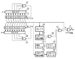
同図において、1は保持するビット列を右方向、左方向の両方向にシフト可能なシフトレジスタ、2はシフトレジスタ1から出力されたビット列をマスクするマスク回路、3はEXOR回路、4はパターンテーブル、5はライン方向セレクタ、6はラインカウンタ、7は画素方向セレクタ、8は画素カウンタ、9は反転回路である。以下の説明では、シフトレジスタ1のビット数をKビット(図1ではK=9)、すなわち、9ビットで表現される乱数を発生する乱数発生器とするが、以下の説明の本質は9ビットに限定するものではない。
In the figure, 1 is a shift register capable of shifting a bit string to be held in both the right and left directions, 2 is a mask circuit for masking a bit string output from the
シフトレジスタ1は保持しているビット列を、乱数を生成する度に1ビット左にシフトする。マスク回路2は、シフトレジスタ1から出力されたビット列のうち、所定のビットのみをマスクしてEXOR回路3に出力する。より具体的には、原始多項式に対応したビット以外をマスクするのであるが、例えば、シフトレジスタ1に「110010100」の9ビットが保持されており(0のインデックスが付けられているメモリ部分には「0」が、1のインデックスが付けられているメモリ部分には「0」が、2のインデックスが付けられているメモリ部分には「1」が、3のインデックスが付けられているメモリ部分には「0」が、4のインデックスが付けられているメモリ部分には「1」が、5のインデックスが付けられているメモリ部分には「0」が、6のインデックスが付けられているメモリ部分には「0」が、7のインデックスが付けられているメモリ部分には「1」が、8のインデックスが付けられているメモリ部分には「1」が保持されている)、原始多項式X7+X+1による乱数を生成する場合には、マスク回路2ではビット6、ビット0以外をマスクし(即ち上記シフトレジスタの値とマスク値「001000001」との論理積をとる)、マスク回路2は「000000000」のビット列を出力する。また、原始多項式X9+X4+1による乱数を生成する場合には、マスク回路2ではビット8、ビット3以外をマスクし(即ち上記シフトレジスタの値とマスク値「100001000」との論理積をとる)、マスク回路2は「100000000」のビット列を出力する。生成されたビット列はEXOR回路3に入力される。
The
EXOR回路3は、マスク回路2から受けたビット列を参照して、フィードバック値を算出する。EXOR回路3はいわゆるパリティビット生成回路と同様の処理を行うものであり、マスク回路2から入力されたビット列において”1”のビット数をカウントし、カウントした数が偶数であれば0を、奇数であれば1を上記フィードバック値として出力する。このフィードバック値は同図の如く、シフトレジスタ1の下位ビット(同図では”0”と示された位置)に入力(フィードバック)される。シフトレジスタ1は、保持しているビット列を左方向に1ビット分シフトした後に、下位ビットにフィードバック値を入力する。そして、シフトレジスタ1は、自身が保持する9ビットのビット列を反転回路9に出力する。
The
従って、上記マスクのパターンを替えることで、K次以下の任意の原始多項式を実現できる。 Therefore, by changing the mask pattern, an arbitrary primitive polynomial of Kth order or lower can be realized.
パターンテーブル4は縦Hビット、横Wビット分のビットを保持するためのメモリであり、同図では縦4ビット、横4ビットの合計16ビットを保持している。各ビットのビット値は0もしくは1である。 The pattern table 4 is a memory for holding bits corresponding to vertical H bits and horizontal W bits. In the figure, the pattern table 4 holds 16 bits in total of 4 vertical bits and 4 horizontal bits. The bit value of each bit is 0 or 1.
ラインカウンタ6は、処理画像のラインに対応したパターンテーブル4のパターンを読み出すためのカウンタである。すなわち、ラインカウンタ6がカウントしているカウント値は、処理しようとする画素が含まれているラインに対応するパターンテーブル4のラインを示している。ラインカウンタ6によるカウント値はセレクタ5に入力される。ラインカウンタ6によるカウント値をcとすると、セレクタ5は、パターンテーブル4においてc列目の各ますに保持されているビット、すなわち4ビットのビット列を読み出して、後段のセレクタ7に出力する。
The
画素カウンタ8は、処理する画素の水平方向の位置に対応したパターンテーブル4のパターンを読み出すためのカウンタである。すなわち、画素カウンタ8がカウントしているカウント値は、処理しようとする画素に対応するラインカウンタ6により選択されたパターンテーブル4のラインデータ中のバターンの位置を示している。画素カウンタ8によるカウント値はセレクタ7に入力される。画素カウンタ8によるカウント値をfとすると、セレクタ7は、セレクタ5から出力された4ビットのビット列においてf個目のビットを読み出して後段の反転回路9に出力する。
The
すなわち、ラインカウンタ6と画素カウンタ8により、パターンテーブル4が保持する16個のビットのうち1つが指定されることになり、指定されたビットが反転回路9に出力される。換言すれば、この指定されたビットは、処理しようとするラインの位置、このラインにおいて処理しようとする画素の位置によって決まる。
That is, one of 16 bits held in the pattern table 4 is designated by the
反転回路9はセレクタ7から出力される1ビットを参照し、参照したビット値が1である場合には、シフトレジスタ1から出力される9ビットのビット列を構成する各ビット値を反転させて外部に出力し、参照したビット値が0である場合には、シフトレジスタ1から出力される9ビットのビット列には何もせずに外部に出力する。このようにして反転回路9からは、9ビットでもって表現される乱数が出力される。
The inverting
以上説明した処理を行えば、処理しようとする画素の位置に応じて、パターンテーブル4が保持する16個のビットのうち、1つが決定され、決定されたビット値に応じて、シフトレジスタ1が保持するビット列の反転/非反転を制御することができる。これにより、シフトレジスタ1が保持するビット列は2次元的に変調される。例えばパターンテーブル4に1010−0101−1010−0101の16ビットを格納すれば、シフトレジスタ1によって生成された乱数の低周波成分は高周波側にシフトされる。
If the processing described above is performed, one of 16 bits held in the pattern table 4 is determined according to the position of the pixel to be processed, and the
また、本実施形態による乱数発生方法によれば、発生する乱数の周期は2×(2K−1)と、従来の周期2K−1の2倍になり、周期の長い一様乱数を生成することができる。
Also, according to the random number generation method according to the present embodiment, the cycle of the generated random number is 2 × (2 K −1), which is twice the
また、上記反転操作により、乱数値が0となる場合(乱数の全ビットが1の値を反転した場合)が発生するが、0が問題となる場合は乱数の全ビットが1のときの反転を禁止するか、0を全ビットが1のデータに置換すれば、従来と同じ一様乱数となる。なお、同じ乱数系列を逆方向に生成するには上記シフトレジスタのシフト方向を逆にし、上記マスクのLSBとMSB(Kビット以下の場合は、最高次数の位置)を交換するだけでよい。 In addition, when the random number value becomes 0 (when all bits of the random number are inverted values of 1) due to the inversion operation, when 0 becomes a problem, the inversion when all the bits of the random number are 1 If 0 is prohibited, or 0 is replaced with data in which all bits are 1, the same uniform random number as before is obtained. In order to generate the same random number sequence in the reverse direction, it is only necessary to reverse the shift direction of the shift register and exchange the LSB and MSB of the mask (the position of the highest order when K bits or less).
[第2の実施形態]
図2は、本実施形態に係る乱数発生器の基本構成を示す図である。なお、同図において図1と同じ部分については同じ番号を付けており、その説明は省略する。図2において11はシフトレジスタ、12はマスク回路、13はEXOR回路、14はパターンテーブル、15はパターン検出回路、16はラインカウンタ、17はセレクタ、18は画素カウンタ、19はEXOR回路、20はパターンカウンタである。
[Second Embodiment]
FIG. 2 is a diagram showing a basic configuration of the random number generator according to the present embodiment. In the figure, the same parts as those in FIG. 1 are denoted by the same reference numerals, and the description thereof is omitted. In FIG. 2, 11 is a shift register, 12 is a mask circuit, 13 is an EXOR circuit, 14 is a pattern table, 15 is a pattern detection circuit, 16 is a line counter, 17 is a selector, 18 is a pixel counter, 19 is an EXOR circuit, and 20 is It is a pattern counter.
シフトレジスタ11、マスク回路12、EXOR回路13はそれぞれシフトレジスタ1、マスク回路2、EXOR回路3と同じで、第1の実施形態で説明したように動作するのであるが、マスク回路12のマスクをマスク回路2のマスクと異ならせることで、上記シフトレジスタ1、マスク回路2、EXOR回路3により生成される乱数と系列(原始多項式)の異なる乱数を生成し、ラインの終端(または先頭)でシフトレジスタ11の値をシフトレジスタ1にロードすることで上記シフトレジスタ1、マスク回路2、EXOR回路3により生成される乱数のライン間の相関性を排除できるようにしたものである。
The
パターンテーブル14にはM系列乱数の周期分(2K−1)のパターンが格納されている。本実施形態ではK=9であるので、パターンテーブル14には511ビット分のビット列のパターンが格納されている。 The pattern table 14 stores patterns of M series random number periods ( 2K- 1). In this embodiment, since K = 9, the pattern table 14 stores a bit string pattern for 511 bits.
画素カウンタ18は、処理しようとする画素の画像上の水平方向の位置に対応したパターンテーブル14の値を選択するためのカウンタである。
The
セレクタ17は、画素カウンタ18の値よりパターンテーブル14に保持されている511ビットのビット列のうち1つを選択して後段の反転回路19に出力する。
The
パターン検出回路15は、シフトレジスタ1、もしくはシフトレジスタ11から出力される9ビットのビット列を参照して、このビット列が予め決められたある特定のパターンのビット列であるか否かを判断する。そしてある特定のパターンである場合には画素カウンタ18がカウントしているカウント値を0にリセットし、パターンカウンタ20のカウント値を反転させる。
The
パターンカウンタ20は、1ビットのカウンタでパターン検出回路15からの指示がない限りは常に同じ値のカウント値(0もしくは1の値)を出力しており、上述の通り、パターン検出回路15がある特定のパターンを検出した場合には、このカウント値を反転する。これにより、乱数列に一意に対応した反転パターンが画素カウンタ18及びセレクタ17によりEXOR回路19に入力される。
The pattern counter 20 is a 1-bit counter and always outputs the same count value (0 or 1) unless there is an instruction from the
ラインカウンタ16は1ビットのカウンタで、ライン毎にカウント値を反転させる。従って、ライン毎にも上記反転パターンは反転されることになる。
The
なお、上記「予め決められたある特定のパターンのビット列」は乱数列と同期をとるためのものであるので、基本的にどのようなパターンのビット列であっても良い。例えば検出を容易にするため、全てのビットが1となるパターンとしても良い。或いは、上記画素カウンタ18を(2K−1)進カウンタとし、カウンタのキャリーでパターンカウンタを反転する構成としても良い。この場合はパターン検出回路15が不要になる。
The above-mentioned “predetermined bit string of a specific pattern” is for synchronizing with a random number string, and therefore may be basically any pattern of bit string. For example, in order to facilitate detection, a pattern in which all bits are 1 may be used. Alternatively, the
そしてEXOR回路19は、セレクタ17からの出力である1ビットとパターンカウンタ20からの出力である1ビットとラインカウンタ16からの出力である1ビットとのEXOR演算を行い、演算結果の1ビットを反転回路9に出力する。反転回路9は、この演算結果の1ビットが1である場合には、シフトレジスタ1からの9ビットを構成する各ビットを反転させてから反転後の9ビットを外部に出力する。一方、EXOR回路19による演算結果の1ビットが0である場合には、シフトレジスタ1からの9ビットをそのまま外部に出力する。
The
上記反転パターンの設定により、用途に応じたスペクトル(周波数特性)を有する乱数が生成可能となる。 By setting the inversion pattern, it is possible to generate a random number having a spectrum (frequency characteristic) according to the application.
上記マスク回路12のマスクパターンをマスク回路2のマスクパターンに一致させることにより、垂直方向に相関を持たせることも、或いは、周期の異なる乱数系列を生成させるようにしても良い。また、ランダム性を向上させるため、上記シフトレジスタ11、マスク回路12、EXOR回路13にて生成される乱数をライン毎にN回生成させてから上記シフトレジスタ1にロードするようにしても良い。特に、シフトレジスタのビット数分(または原始多項式の最高次数分)乱数を空生成させてから上記シフトレジスタ1にロードすれば、ライン間の相関はなくなる。
By matching the mask pattern of the
また、上記パターンテーブル14を2次元化し、空間周波数を整形するようにしても良い。この場合は、ラインカウンタ16をシフトレジスタ11、マスク回路12、EXOR回路13にて構成される乱数の周期に合わせ、パターンテーブル14のラインの選択に用いる。なお、EXOR回路19はラインカウンタ16による反転は不要になるので、2入力で良い。
The pattern table 14 may be two-dimensional and the spatial frequency may be shaped. In this case, the
[第3の実施形態]
図3は、本実施形態に係る乱数発生器の基本構成を示す図である。同図において図1,2と同じ部分については同じ番後を付けており、その説明は省略する。同図において、21,22はEXOR回路、23,24,25はセレクタ、26はパターン検出回路、27は画素カウンタ、28はEXOR回路である。
[Third Embodiment]
FIG. 3 is a diagram showing a basic configuration of the random number generator according to the present embodiment. In the figure, the same parts as those shown in FIGS. In the figure, 21 and 22 are EXOR circuits, 23, 24 and 25 are selectors, 26 is a pattern detection circuit, 27 is a pixel counter, and 28 is an EXOR circuit.
セレクタ23は、シフトレジスタ11からの9ビットを受け、このうち9ビット以下の所定数のビット(同図では4ビット)を選択してEXOR回路21に入力する。EXOR回路21は、入力された4ビットのビット列中の1の数が偶数であれば0を、奇数であれば1を出力し、シフトレジスタ11に入力する。9次以下の原始多項式の+1項を除く項数の最大値は4であるので、EXOR回路21は4入力で充分である。なお、3項選択時は残りの入力として0を選択し、2項選択時は残りの入力に0を選択するか、同じビットを残りの入力として選択する。
The
同様に、セレクタ24は、シフトレジスタ1からの9ビットを受け、このうち9ビット以下の所定数のビット(同図では4ビット)を選択してEXOR回路22に入力する。EXOR回路22は、入力された4ビットのビット列中の1の数が偶数であれば0を、奇数であれば1を出力し、シフトレジスタ1に入力する。
Similarly, the
セレクタ25はシフトレジスタ1からの9ビットのビット列のうち原始多項式の最高次数に対応するビットから所定ビット数分のビット列を抽出して後段のパターン検出回路26に入力する。
The
パターン検出回路26は、セレクタ25から入力された所定ビット数分のビット列がある特定のパターンのビット列に一致するものであるか否かを判断し、一致する場合には1のビットを後段のEXOR回路28に入力し、一致しない場合には0のビットをEXOR回路28に入力する。
The
一方、画素カウンタ27は1ビットのデータを保持しており、乱数列が発生される度にその1ビットを反転させる。すなわち、乱数列が生成される毎に、0,1,0,1,,,というように、0と1を交互に出力することになる。画素カウンタ27によるカウント値はEXOR回路28に入力される。
On the other hand, the
EXOR回路28はパターン検出回路26からの1ビットと画素カウンタ27からの1ビットとのEXOR演算を行い、演算結果の1ビットを後段のEXOR回路19に出力する。すなわちEXOR回路28は、セレクタ25から入力された所定ビット数分のビット列がある特定のパターンのビット列に一致するものである場合には、画素カウンタ27からのビットを反転させる処理を行い、その反転後のビットを後段のEXOR回路19に出力することになる。
The
例えば、最高次数から4ビットの値が0101の場合、M系列乱数ではシフトレジスタを用いているため以降の乱数のMSBは0101の順となる。画素カウンタ27によるカウント値は乱数が生成される度に反転するので、例えば生成した乱数のMSBが0101…の順に出力され、この値に上記反転操作を行った場合、出力される乱数のMSBは0000と連続して同じ値になってしまう。これは、乱数の高周波成分が低周波側に変調されることを意味し、視覚的に検知され易くなる。そこで、乱数のMSB側から所定ビット数分を抽出し、0101のようなパターンを検出して画素カウンタ27の値を反転し、乱数が低周波側に変調されないようにするのである。
For example, if the 4-bit value from the highest order is 0101, the M-sequence random numbers use a shift register, and the MSBs of the subsequent random numbers are in the order of 0101. Since the count value by the
図5は、4次の原始多項式x4+x+1の場合のMSBを示す図である。同図に示す如く、上記変更前はサイクル4から8までのMSBが0となっているが(before項参照)、0101パターンの検出による反転を行うと(after項参照)、MSBの0の連続数及び1の連続数は3以下に抑えられていることがわかる。これは上記原始多項式にかかわらず、他の原始多項式においてもMSBの0の連続数及び1の連続数は3以下に抑えられる。なお、0000を1111に置き換えれば、上記30サイクル中に同じ値は2度づつ発生しているので、一様乱数となっており、かつ周期が2倍になっていることがわかる。また、EXORの代わりにEXNORを用いても良い。この場合は1111(全てのビットが1)を0000に置き換えればよい。
FIG. 5 is a diagram illustrating the MSB in the case of a fourth-order primitive polynomial x 4 + x + 1. As shown in the figure, the MSB from
また、上記セレクタ24を上記パターン同期信号(パターン検出回路15の出力または2K−1進カウンタのキャリー)にて切替えるようにすることで、異なる原始多項式に順次切替えてゆくことが可能となる。これにより一様乱数の特性を維持しつつ周期をさらに拡大することが可能となる。なお、ライン方向の周期の拡大も上記セレクタ23を切替えることで実現できる。この時の切替えのタイミングはシフトレジスタ11のシフト動作がとまっている時であれば良いので、容易に切替えが可能である。
Further, by switching the
そしてEXOR回路19は、入力された全てのビット値に対するEXOR演算処理を行い、その演算結果である1ビットを反転回路9に入力する。以降の処理については第1の実施形態と同じである。
The
なお、本実施形態ではEXOR回路21、22は4入力としているが、これに限らず例えば2入力としても良い。この場合は一部(ここでは8次)の原始多項式の実現ができなくなるが、実現できなきなる原始多項式の数は少ないので、大きな支障はない。
In the present embodiment, the
[第4の実施形態]
図4は、本実施形態に係る乱数発生器の構成を示す図である。同図において図2,3と同じ部分については同じ番号を付けており、その説明は省略する。同図において、31,34はシフトレジスタ、32,35はマスク回路、33,36はEXOR回路、29はMSBテーブル、30はラインカウンタである。
[Fourth Embodiment]
FIG. 4 is a diagram illustrating a configuration of the random number generator according to the present embodiment. In the figure, the same parts as those in FIGS. 2 and 3 are denoted by the same reference numerals, and the description thereof is omitted. In the figure, 31 and 34 are shift registers, 32 and 35 are mask circuits, 33 and 36 are EXOR circuits, 29 is an MSB table, and 30 is a line counter.
シフトレジスタ31、マスク回路32、EXOR回路33により構成されるLFSRによってライン毎に乱数を生成する処理については上記実施形態と同じである。これはシフトレジスタ34,マスク回路35,EXOR回路36により構成されるLFSRについても同じである。本実施形態では乱数のMSBはMSBテーブル29を変調して生成するので、上記LFSRでもって扱うビット列のビット数は1ビット少なくなる。
The processing for generating a random number for each line by the LFSR configured by the
ラインカウンタ30はMSBテーブル29のラインを選択するためのカウンタで、ラインカウンタ16と同様にしてラインが切り替わる毎に順次カウントアップし、MSBテーブル29のライン数に達するとカウント値を0にリセットし、MSBテーブル29のライン数分のカウントを繰り返す。
The
MSBテーブル29には2次元的に乱数のMSBが格納されており、ラインカウンタ30及び画素カウンタ18とセレクタ17により1つのMSBが選択される。この選択については、第1の実施形態と同様に、ラインカウンタでもって列を特定し、画素カウンタ18でもってこの列のうちの1つのビットを選択することにより成される。
The MSB table 29 stores two-dimensional random number MSBs, and one MSB is selected by the
そしてEXOR回路19は、セレクタ17からの1ビットとパターン検出回路15、パターンカウンタ20による1ビットとのEXOR演算処理を行い、その演算結果である1ビットを出力する。そして出力されたこの1ビットをシフトレジスタ31もしくはシフトレジスタ34からの8ビットのビット列の先頭にMSBとして付加し、合計9ビットのビット列を外部に出力する。
The
以上の構成により、MSBテーブル29の画素方向のサイズをシフトレジスタ34、マスク回路35、EXOR回路36にて構成される乱数の周期に一致させ、また、ライン方向のサイズは、シフトレジスタ31、マスク回路32、EXOR回路33にて構成される乱数の周期に一致させることで、所望の空間周波数特性を持った乱数を生成させることができる。
With the above configuration, the size in the pixel direction of the MSB table 29 is made to coincide with the cycle of the random number formed by the
[第5の実施形態]
第1乃至4の実施形態で説明した乱数発生方法は、図1乃至4に示す如く構成を備えるハードウェアでもって実行していたが、メモリとして機能する部分をコンピュータのRAM内に設け、メモリとして機能する部分以外のそれぞれの部分を、それぞれの部分の機能をコンピュータのCPUに実行させるためのプログラムの形態でもって実装するようにしても良い。すなわち、第1乃至4の実施形態で説明した乱数発生方法をソフトウェアの形態でもって実装し、これをコンピュータに実行させることで、このコンピュータが上記各実施形態で説明した乱数発生方法を実現させるようにしても良い。その場合、このコンピュータの構成としては周知のPC(パーソナルコンピュータ)やWS(ワークステーション)等が適用可能であり、これらのコンピュータは周知の通り、CPUやRAMを備える、また、これ以外の構成については特に限定するものではない。
[Fifth Embodiment]
The random number generation method described in the first to fourth embodiments is executed by hardware having a configuration as shown in FIGS. 1 to 4. However, a part that functions as a memory is provided in a RAM of a computer and is used as a memory. Each part other than the functioning part may be implemented in the form of a program for causing the CPU of the computer to execute the function of each part. That is, the random number generation method described in the first to fourth embodiments is implemented in the form of software, and this is executed by a computer so that the computer realizes the random number generation method described in each of the above embodiments. Anyway. In that case, a well-known PC (personal computer), WS (workstation), or the like can be applied as the configuration of the computer. As is well known, these computers include a CPU and a RAM. Is not particularly limited.
また、このソフトウェアのプログラムをコンピュータに供給する方法についても特に限定するものではなく、周知の通り、ハードディスクドライブ装置からRAMにロードするようにしても良いし、LANやインターネットなどのネットワークを介して外部装置からこのコンピュータのRAMにこのソフトウェアのプログラムを供給するようにしても良い。 Further, the method of supplying the software program to the computer is not particularly limited. As is well known, the software program may be loaded from the hard disk drive device to the RAM, or externally via a network such as a LAN or the Internet. The software program may be supplied from the apparatus to the RAM of the computer.
[その他の実施形態]
本発明の目的は、前述した実施形態の機能を実現するソフトウェアのプログラムコードを記録した記録媒体(または記憶媒体)を、カメラやプリンタ等の機器のCPUやMPUが記録媒体に格納されたプログラムコードを読み出し実行することによっても、達成されることは言うまでもない。この場合、記録媒体から読み出されたプログラムコード自体が前述した実施形態の機能を実現することになり、そのプログラムコードを記録した記録媒体は本発明を構成することになる。
[Other Embodiments]
An object of the present invention is to provide a recording medium (or storage medium) that records a program code of software that realizes the functions of the above-described embodiments, and a program code in which a CPU or MPU of a device such as a camera or printer is stored in the recording medium. Needless to say, this can also be achieved by reading and executing. In this case, the program code itself read from the recording medium realizes the functions of the above-described embodiment, and the recording medium on which the program code is recorded constitutes the present invention.
また、カメラやプリンタ等の機器が読み出したプログラムコードを実行することにより、前述した実施形態の機能が実現されるだけでなく、そのプログラムコードの指示に基づき、カメラやプリンタ等の機器上で稼働しているオペレーティングシステム(OS)などが実際の処理の一部または全部を行い、その処理によって前述した実施形態の機能が実現される場合も含まれることは言うまでもない。 Also, by executing the program code read by the device such as the camera or the printer, not only the functions of the above-described embodiment are realized, but also the operation is performed on the device such as the camera or the printer based on the instruction of the program code. It goes without saying that the operating system (OS) or the like performing part or all of the actual processing and realizing the functions of the above-described embodiments by the processing.
さらに、記録媒体から読み出されたプログラムコードが、カメラやプリンタ等の機器に挿入された機能拡張カードやカメラやプリンタ等の機器に接続された機能拡張ユニットに備わるメモリに書込まれた後、そのプログラムコードの指示に基づき、その機能拡張カードや機能拡張ユニットに備わるCPUなどが実際の処理の一部または全部を行い、その処理によって前述した実施形態の機能が実現される場合も含まれることは言うまでもない。 Furthermore, after the program code read from the recording medium is written into a memory provided in a function expansion card inserted in a device such as a camera or printer or a function expansion unit connected to a device such as a camera or printer, This includes the case where the CPU of the function expansion card or function expansion unit performs part or all of the actual processing based on the instruction of the program code, and the functions of the above-described embodiments are realized by the processing. Needless to say.
本発明を上記記録媒体に適用する場合、その記録媒体には、先に説明した機能構成に対応するプログラムコードが格納されることになる。 When the present invention is applied to the recording medium, the recording medium stores a program code corresponding to the functional configuration described above.
Claims (11)
マスクパターンを表すビットパターンを生成して設定する設定工程と、
メモリに保持されているKビットのビット列を前記ビットパターンでマスクするマスク工程と、
前記マスク工程でマスクしたビット列に対する排他的論理和演算を行い、当該排他的論理和演算結果を示すビット値を、前記メモリに保持されているKビットのビット列を予め定められた方向にシフトした結果に含める演算工程と、
予め設定されたビットパターン中の指示されたビット値に応じて、前記演算工程によるビット列中の各ビット値の反転/非反転を制御する第1の反転制御工程と、
前記第1の反転制御工程による処理結果のビット列を、Kビットで表現される乱数として出力する出力工程と
を備えることを特徴とする乱数発生方法。 A random number generation method for generating a random number expressed in K bits,
A setting step for generating and setting a bit pattern representing a mask pattern;
A masking step of masking a bit string of K bits held in memory in the bit pattern,
A result of performing an exclusive OR operation on the bit string masked in the masking process, and shifting a bit value indicating the exclusive OR operation result in a predetermined direction to a bit string of K bits held in the memory A calculation process to be included in
A first inversion control step for controlling inversion / non-inversion of each bit value in the bit string by the calculation step in accordance with an instructed bit value in a preset bit pattern;
A random number generation method comprising: an output step of outputting a bit string as a result of processing in the first inversion control step as a random number represented by K bits.
マスクパターンを表すビットパターンを生成して設定する設定工程と、
メモリに保持されている(K−1)ビットのビット列を前記ビットパターンでマスクするマスク工程と、
前記マスク工程でマスクしたビット列に対する排他的論理和演算を行い、当該排他的論理和演算結果を示すビット値を、前記メモリに保持されている(K−1)ビットのビット列を予め定められた方向にシフトした結果に含める第1の演算工程と、
処理する画素の画像上の位置に応じて、前記予め設定されたビットパターン中のビット値を選択する選択工程と、
処理する画素の画像上の位置に応じて、前記選択工程で選択されたビット値を反転させる処理を制御する反転制御工程と、
前記第1の演算工程によるビット列の先頭に前記反転制御工程での処理結果のビットを付加したことにより得られるビット列を、Kビットで表現される乱数として出力する出力工程と
を備えることを特徴とする乱数発生方法。 A random number generation method for generating a random number expressed in K bits,
A setting step for generating and setting a bit pattern representing a mask pattern;
A masking step of masking is held in the memory (K-1) bit string in the bit pattern,
An exclusive OR operation is performed on the bit string masked in the masking step, and a bit value indicating the exclusive OR operation result is stored in the memory in a predetermined direction as a bit string of (K-1) bits. A first calculation step to be included in the result of shifting to
A selection step of selecting a bit value in the preset bit pattern according to the position of the pixel to be processed on the image;
An inversion control step for controlling processing for inverting the bit value selected in the selection step according to the position of the pixel to be processed on the image
An output step of outputting a bit string obtained by adding the bit of the processing result in the inversion control step to the head of the bit string in the first calculation step as a random number represented by K bits, How to generate random numbers.
Kビットのビット列を保持するレジスタと、
マスクパターンを表すビットパターンを生成して設定する設定手段と、
前記レジスタが保持するビット列を前記ビットパターンでマスクするマスク手段と、
前記レジスタが保持するビット列を予め定められた方向にシフトするシフト手段と、
前記マスク手段がマスクしたビット列に対する排他的論理和演算を行い、当該排他的論理和演算結果を示すビット値を、前記シフト手段がシフトした前記レジスタ内のビット列に含める演算手段と、
予め設定されたビットパターン中の指示されたビット値に応じて、前記演算手段によるビット列中の各ビット値を反転させる処理を制御する第1の反転制御手段と、
前記第1の反転制御手段による処理結果のビット列を、Kビットで表現される乱数として出力する出力手段と
を備えることを特徴とする乱数発生装置。 A random number generator for generating a random number expressed in K bits,
A register holding a bit string of K bits;
Setting means for generating and setting a bit pattern representing a mask pattern;
A mask means for masking the bit string with the bit pattern which the register holds,
Shift means for shifting the bit string held by the register in a predetermined direction;
An arithmetic means for performing an exclusive OR operation on the bit string masked by the mask means, and including a bit value indicating the result of the exclusive OR operation in the bit string in the register shifted by the shift means;
First inversion control means for controlling processing for inverting each bit value in the bit string by the arithmetic means in accordance with an instructed bit value in a preset bit pattern;
A random number generator comprising: output means for outputting a bit string of a processing result by the first inversion control means as a random number represented by K bits.
(K−1)ビットのビット列を保持するレジスタと、
マスクパターンを表すビットパターンを生成して設定する設定手段と、
前記レジスタが保持するビット列を前記ビットパターンでマスクするマスク手段と、
前記レジスタが保持するビット列を予め定められた方向にシフトするシフト手段と、
前記マスク手段がマスクしたビット列に対する排他的論理和演算を行い、当該排他的論理和演算結果を示すビット値を、前記シフト手段がシフトした前記レジスタ内のビット列に含める第1の演算手段と、
前記第1の演算手段によるビット列中の予め定められたビット数分のビット列がある特定のビット列であるか否かに応じて決まるビット値と、予め設定されたビットパターン中の指示されたビット値とに応じて決まるビット値を演算する第2の演算手段と、
前記第1の演算手段で演算されたビット列の先頭に前記第2の演算手段によるビットを付加したことにより得られるビット列を、Kビットで表現される乱数として出力する出力手段と
を備えることを特徴とする乱数発生装置。 A random number generator for generating a random number expressed in K bits,
(K-1) a register for holding a bit string of bits;
Setting means for generating and setting a bit pattern representing a mask pattern;
A mask means for masking the bit string with the bit pattern which the register holds,
Shift means for shifting the bit string held by the register in a predetermined direction;
First arithmetic means for performing an exclusive OR operation on the bit string masked by the mask means, and including a bit value indicating the exclusive OR result in the bit string in the register shifted by the shift means;
A bit value determined depending on whether or not a bit string corresponding to a predetermined number of bits in the bit string by the first arithmetic means is a specific bit string, and an indicated bit value in a preset bit pattern Second calculating means for calculating a bit value determined according to
Output means for outputting a bit string obtained by adding a bit by the second calculating means to the head of the bit string calculated by the first calculating means as a random number represented by K bits. Random number generator.
Kビットのビット列を保持する第1のレジスタと、
前記レジスタが保持するビット列から予め定められたビット列を選択する第1の選択手段と、
前記レジスタが保持するビット列を予め定められた方向にシフトする第1のシフト手段と、
前記第1の選択手段が選択したビット列に対する排他的論理和演算を行い、当該排他的論理和演算結果を示すビット値を、前記第1のシフト手段がシフトした前記第1のレジスタ内のビット列に含める第1の演算手段と、
前記第1の演算手段によるビット列中の予め定められたビット数分のビット列が、ある特定のビット列であるか否かに応じて決まるビット値と、処理する画素の画像上の位置に応じて、前記第1の演算手段によるビット列中の各ビットの値を反転させる処理を制御する反転制御手段と、
前記反転制御手段による処理結果のビット列を、Kビットで表現される乱数として出力する出力手段と
を備えることを特徴とする乱数発生装置。 A random number generator for generating a random number expressed in K bits,
A first register holding a bit string of K bits;
First selection means for selecting a predetermined bit string from the bit string held by the register;
First shift means for shifting the bit string held by the register in a predetermined direction;
An exclusive OR operation is performed on the bit string selected by the first selection unit, and a bit value indicating the result of the exclusive OR operation is added to the bit string in the first register shifted by the first shift unit. First computing means to include;
According to the bit value determined according to whether or not the bit string for a predetermined number of bits in the bit string by the first arithmetic means is a specific bit string, and the position of the pixel to be processed on the image, Inversion control means for controlling processing for inverting the value of each bit in the bit string by the first arithmetic means;
A random number generator comprising: output means for outputting a bit string of a processing result by the inversion control means as a random number represented by K bits.
前記第2のレジスタが保持するビット列から予め定められたビット列を選択する第2の選択手段と、
前記第2のレジスタが保持するビット列を予め定められた方向にシフトする第2のシフト手段と、
前記第2の選択手段が選択したビット列に対する排他的論理和演算を行い、当該排他的論理和演算結果を示すビット値を、前記第2のシフト手段がシフトした前記第2のレジスタ内のビット列に含める第2の演算手段とを備え、
処理する画像上のライン終端またはライン先頭にて、前記第1のレジスタに前記第2のレジスタの値をロードすることを特徴とする請求項8に記載の乱数発生装置。 A second register holding a bit string of K bits;
Second selection means for selecting a predetermined bit string from the bit string held by the second register;
Second shift means for shifting the bit string held by the second register in a predetermined direction;
An exclusive OR operation is performed on the bit string selected by the second selection means, and a bit value indicating the exclusive OR operation result is converted into a bit string in the second register shifted by the second shift means. A second calculating means to include,
9. The random number generator according to claim 8 , wherein the value of the second register is loaded into the first register at the end of the line or the top of the line on the image to be processed.
メモリに保持されているKビットのビット列から予め定められたビット列を選択する第1の選択工程と、
前記メモリが保持するビット列を予め定められた方向にシフトする第1のシフト工程と、
前記第1の選択工程で選択したビット列に対する排他的論理和演算を行い、当該排他的論理和演算結果を示すビット値を、前記第1のシフト工程でシフトした前記メモリ内のビット列に含める第1の演算工程と、
前記第1の演算工程によるビット列中の予め定められたビット数分のビット列が、ある特定のビット列であるか否かに応じて決まるビット値と、処理する画素の画像上の位置に応じて、前記第1の演算工程によるビット列中の各ビットの値を反転させる処理を制御する反転制御工程と、
前記反転制御工程による処理結果のビット列を、Kビットで表現される乱数として出力する出力工程と
を備えることを特徴とする乱数発生方法。 A random number generation method for generating a random number expressed in K bits,
A first selection step of selecting a predetermined bit string from a K-bit bit string held in a memory;
A first shift step of shifting a bit string held in the memory in a predetermined direction;
A first logical OR operation is performed on the bit string selected in the first selection step, and a bit value indicating the result of the exclusive OR operation is included in the bit string in the memory shifted in the first shift step. And the calculation process of
According to a bit value determined according to whether or not a predetermined number of bit strings in the bit string by the first calculation step is a specific bit string, and a position on the image of a pixel to be processed, An inversion control step for controlling a process of inverting the value of each bit in the bit string in the first calculation step;
A random number generation method comprising: an output step of outputting a bit string of a processing result obtained by the inversion control step as a random number represented by K bits.
当該メモリが保持するビット列を予め定められた方向にシフトする第2のシフト工程と、
前記第2の選択工程で選択したビット列に対する排他的論理和演算を行い、当該排他的論理和演算結果を示すビット値を、前記第2のシフト工程でシフトした当該メモリ内のビット列に含める第2の演算工程とを備え、
処理する画像上のライン終端またはライン先頭にて、前記第1のレジスタに前記第2のレジスタの値をロードすることを特徴とする請求項10に記載の乱数発生方法。 A second selection step of selecting a predetermined bit string from a K-bit bit string held in the memory;
A second shift step of shifting the bit string held in the memory in a predetermined direction;
A second OR is performed on the bit string selected in the second selection step, and the bit value indicating the result of the exclusive OR operation is included in the bit string in the memory shifted in the second shift step. With the calculation process of
11. The random number generation method according to claim 10 , wherein a value of the second register is loaded into the first register at a line end or a line head on an image to be processed.
Priority Applications (3)
| Application Number | Priority Date | Filing Date | Title |
|---|---|---|---|
| JP2004174607A JP4418713B2 (en) | 2004-06-11 | 2004-06-11 | Random number generation method and random number generator |
| US11/149,133 US7895251B2 (en) | 2004-06-11 | 2005-06-10 | Random number generating method and random number generating apparatus |
| US13/013,770 US8782108B2 (en) | 2004-06-11 | 2011-01-25 | Random number generating method and random number generating apparatus |
Applications Claiming Priority (1)
| Application Number | Priority Date | Filing Date | Title |
|---|---|---|---|
| JP2004174607A JP4418713B2 (en) | 2004-06-11 | 2004-06-11 | Random number generation method and random number generator |
Publications (3)
| Publication Number | Publication Date |
|---|---|
| JP2005352904A JP2005352904A (en) | 2005-12-22 |
| JP2005352904A5 JP2005352904A5 (en) | 2007-07-19 |
| JP4418713B2 true JP4418713B2 (en) | 2010-02-24 |
Family
ID=35461790
Family Applications (1)
| Application Number | Title | Priority Date | Filing Date |
|---|---|---|---|
| JP2004174607A Expired - Fee Related JP4418713B2 (en) | 2004-06-11 | 2004-06-11 | Random number generation method and random number generator |
Country Status (2)
| Country | Link |
|---|---|
| US (2) | US7895251B2 (en) |
| JP (1) | JP4418713B2 (en) |
Families Citing this family (13)
| Publication number | Priority date | Publication date | Assignee | Title |
|---|---|---|---|---|
| JP4418713B2 (en) * | 2004-06-11 | 2010-02-24 | キヤノン株式会社 | Random number generation method and random number generator |
| FR2899702A1 (en) * | 2006-04-10 | 2007-10-12 | France Telecom | METHOD AND DEVICE FOR GENERATING A PSEUDO-RANDOM SUITE |
| US8788552B2 (en) * | 2008-01-25 | 2014-07-22 | Tata Consultancy Services Ltd. | Deterministic random number generator for cryptography and digital watermarking |
| DE112008003878T5 (en) * | 2008-05-21 | 2011-05-05 | Verigy (Singapore) Pte. Ltd. | Method and apparatus for the determination of a repetitive bit value pattern |
| US9747105B2 (en) * | 2009-12-17 | 2017-08-29 | Intel Corporation | Method and apparatus for performing a shift and exclusive or operation in a single instruction |
| JP5836585B2 (en) * | 2010-02-09 | 2015-12-24 | キヤノン株式会社 | Data processing apparatus, control method therefor, and program |
| US8918442B2 (en) * | 2012-08-22 | 2014-12-23 | International Business Machines Corporation | Reducing bias in hardware generated random numbers |
| JP2014222394A (en) | 2013-05-13 | 2014-11-27 | 株式会社東芝 | Semiconductor storage device and random number generator |
| JP6542171B2 (en) * | 2016-09-15 | 2019-07-10 | 東芝メモリ株式会社 | Randomizer and semiconductor memory device |
| CN112955955B (en) * | 2018-10-24 | 2023-01-31 | 宁波飞芯电子科技有限公司 | Counting method, counting device, counting system using counting device and pixel array |
| GB2580160B (en) | 2018-12-21 | 2021-01-06 | Graphcore Ltd | Hardware module for converting numbers |
| KR102199808B1 (en) * | 2019-03-26 | 2021-01-07 | 한양대학교 에리카산학협력단 | Method and device for generating a true random number based on sensors of drone |
| WO2021257817A1 (en) * | 2020-06-17 | 2021-12-23 | The Trustees Of Princeton University | System and method for secure and robust distributed deep learning |
Family Cites Families (10)
| Publication number | Priority date | Publication date | Assignee | Title |
|---|---|---|---|---|
| JP3568551B2 (en) | 1993-03-18 | 2004-09-22 | アンリツ株式会社 | Pseudo random signal generator |
| DE69631948T2 (en) | 1995-12-21 | 2005-02-10 | Canon K.K. | Image processing apparatus and method |
| JP3461247B2 (en) | 1996-07-19 | 2003-10-27 | キヤノン株式会社 | Image processing apparatus and image processing method |
| JPH11340799A (en) * | 1998-05-28 | 1999-12-10 | Oki Electric Ind Co Ltd | Circuit and method for generating m sequence and circuit for generating pn sequence |
| JPH11339016A (en) * | 1998-05-28 | 1999-12-10 | Canon Inc | Image processor, image processing method and memory medium |
| JP3613396B2 (en) * | 2001-06-25 | 2005-01-26 | 日本電気株式会社 | Function block |
| DE10216240A1 (en) * | 2002-04-12 | 2003-10-30 | Infineon Technologies Ag | Method and device for calculating an iterated state of a feedback shift register arrangement |
| US7028059B2 (en) * | 2002-06-24 | 2006-04-11 | Sun Microsystems, Inc. | Apparatus and method for random number generation |
| US20040078401A1 (en) * | 2002-10-22 | 2004-04-22 | Hilton Howard E. | Bias-free rounding in digital signal processing |
| JP4418713B2 (en) * | 2004-06-11 | 2010-02-24 | キヤノン株式会社 | Random number generation method and random number generator |
-
2004
- 2004-06-11 JP JP2004174607A patent/JP4418713B2/en not_active Expired - Fee Related
-
2005
- 2005-06-10 US US11/149,133 patent/US7895251B2/en not_active Expired - Fee Related
-
2011
- 2011-01-25 US US13/013,770 patent/US8782108B2/en not_active Expired - Fee Related
Also Published As
| Publication number | Publication date |
|---|---|
| US7895251B2 (en) | 2011-02-22 |
| US8782108B2 (en) | 2014-07-15 |
| JP2005352904A (en) | 2005-12-22 |
| US20110119321A1 (en) | 2011-05-19 |
| US20050278402A1 (en) | 2005-12-15 |
Similar Documents
| Publication | Publication Date | Title |
|---|---|---|
| US7895251B2 (en) | Random number generating method and random number generating apparatus | |
| JP2937919B2 (en) | Pseudo random number generator | |
| JP3022439B2 (en) | Pseudo random number generation method and apparatus | |
| JP2008145791A5 (en) | ||
| JP2004007337A5 (en) | ||
| US20080304667A1 (en) | Method and Apparatus For Cellular Automata Based Generation of Pseudorandom Sequences With Controllable Period | |
| JP2004534266A (en) | Method and apparatus for efficiently performing arithmetic operations in hardware | |
| JP2002040933A (en) | Ciphering device using standard algorithm for ciphering data | |
| US20060156187A1 (en) | Method and apparatus for multiple polynomial-based random number generation | |
| JP2004258141A (en) | Arithmetic unit for multiple length arithmetic of montgomery multiplication residues | |
| KR100478974B1 (en) | Serial finite-field multiplier | |
| JP2005352904A5 (en) | ||
| US9389834B2 (en) | Pseudorandom number generating circuit and method | |
| JP3823107B2 (en) | Basis transformation method and basis transformation device in finite field | |
| JP3626105B2 (en) | Pseudo random signal generation circuit | |
| JP2014222394A (en) | Semiconductor storage device and random number generator | |
| JP2010160248A (en) | Gold sequence pseudo-random number generating circuit | |
| JP2022103663A (en) | Image processing device, image processing method of image processing device and program | |
| JPH07134647A (en) | Random number generator | |
| JP2009301265A (en) | Multiple determination method, multiple deciding device, and multiple determination program | |
| RU2761766C1 (en) | Apparatus for generating pseudorandom numbers | |
| JP3157741B2 (en) | Binary-decimal conversion circuit | |
| JP3806762B2 (en) | Random number generator, random number generation method and program | |
| JP3610564B2 (en) | Information processing device | |
| JP3618554B2 (en) | Code generation method and code generation apparatus |
Legal Events
| Date | Code | Title | Description |
|---|---|---|---|
| A521 | Request for written amendment filed |
Free format text: JAPANESE INTERMEDIATE CODE: A523 Effective date: 20070531 |
|
| A621 | Written request for application examination |
Free format text: JAPANESE INTERMEDIATE CODE: A621 Effective date: 20070531 |
|
| RD03 | Notification of appointment of power of attorney |
Free format text: JAPANESE INTERMEDIATE CODE: A7423 Effective date: 20070531 |
|
| A131 | Notification of reasons for refusal |
Free format text: JAPANESE INTERMEDIATE CODE: A131 Effective date: 20090724 |
|
| A521 | Request for written amendment filed |
Free format text: JAPANESE INTERMEDIATE CODE: A523 Effective date: 20090924 |
|
| TRDD | Decision of grant or rejection written | ||
| A01 | Written decision to grant a patent or to grant a registration (utility model) |
Free format text: JAPANESE INTERMEDIATE CODE: A01 Effective date: 20091124 |
|
| A01 | Written decision to grant a patent or to grant a registration (utility model) |
Free format text: JAPANESE INTERMEDIATE CODE: A01 |
|
| A61 | First payment of annual fees (during grant procedure) |
Free format text: JAPANESE INTERMEDIATE CODE: A61 Effective date: 20091130 |
|
| R150 | Certificate of patent or registration of utility model |
Free format text: JAPANESE INTERMEDIATE CODE: R150 |
|
| FPAY | Renewal fee payment (event date is renewal date of database) |
Free format text: PAYMENT UNTIL: 20121204 Year of fee payment: 3 |
|
| FPAY | Renewal fee payment (event date is renewal date of database) |
Free format text: PAYMENT UNTIL: 20131204 Year of fee payment: 4 |
|
| LAPS | Cancellation because of no payment of annual fees |