JP4403000B2 - Microchip and micropump - Google Patents
Microchip and micropump Download PDFInfo
- Publication number
- JP4403000B2 JP4403000B2 JP2004097638A JP2004097638A JP4403000B2 JP 4403000 B2 JP4403000 B2 JP 4403000B2 JP 2004097638 A JP2004097638 A JP 2004097638A JP 2004097638 A JP2004097638 A JP 2004097638A JP 4403000 B2 JP4403000 B2 JP 4403000B2
- Authority
- JP
- Japan
- Prior art keywords
- valve
- substrate
- pdms
- fine
- microchip
- Prior art date
- Legal status (The legal status is an assumption and is not a legal conclusion. Google has not performed a legal analysis and makes no representation as to the accuracy of the status listed.)
- Expired - Fee Related
Links
Images


Description
本発明は遺伝子解析などの化学/生化学分析などに広く使用されるマイクロ流体制御機構付マイクロチップに関する。更に詳細には、本発明はマイクロチップの基板内に形成された微細流路(マイクロチャネル)や反応容器内における流体の移送を制御するための逆止弁として機能するマイクロバルブに関する。 The present invention relates to a microchip with a microfluidic control mechanism widely used for chemical / biochemical analysis such as gene analysis. More specifically, the present invention relates to a microchannel that functions as a check valve for controlling the flow of fluid in a microchannel or a reaction vessel formed in a microchip substrate.
最近、マイクロスケール・トータル・アナリシス・システムズ(μTAS)又はラブ・オン・チップ(Lab-on-Chip)などの名称で知られるように、基板内にマイクロチャネルや反応容器及びポートなどの微細構造を設け、該微細構造内で物質の化学反応、合成、精製、抽出、生成及び/又は分析など各種の操作を行うように構成されたマイクロデバイスが提案され、一部実用化されている。このような目的のために製作された、基板内にマイクロチャネル、ポート及び反応容器などの微細構造を有する構造物は総称して「マイクロチップ」又は「マイクロ流体デバイス」と呼ばれる。マイクロチップは遺伝子解析、臨床診断、薬物スクリーニングなどの化学、生化学、薬学、医学、獣医学分野のみならず、化学工業、環境計測などの幅広い用途に使用できる。常用サイズの同種の装置に比べて、マイクロチップは(1)サンプル及び試薬の使用量が著しく少ない、(2)分析時間が短い、(3)感度が高い、(4)現場に携帯し、その場で分析できる、及び(5)使い捨てできるなどの利点を有する。 Microstructures such as microchannels, reaction vessels, and ports have been built into the substrate as is known recently under the name of Microscale Total Analysis Systems (μTAS) or Lab-on-Chip (Lab-on-Chip). A microdevice configured to perform various operations such as chemical reaction, synthesis, purification, extraction, generation and / or analysis of a substance within the microstructure has been proposed and partially put into practical use. Structures manufactured for this purpose and having a microstructure such as microchannels, ports and reaction vessels in the substrate are collectively referred to as “microchips” or “microfluidic devices”. Microchips can be used in a wide range of applications such as chemical industry and environmental measurement as well as chemical, biochemical, pharmaceutical, medical, and veterinary fields such as gene analysis, clinical diagnosis, and drug screening. Compared with the same type of equipment of the common size, the microchip is (1) significantly less sample and reagent usage, (2) shorter analysis time, (3) higher sensitivity, (4) carried on-site, It can be analyzed in the field and (5) can be disposable.
従来のマイクロチップ100は、例えば、図13A及びBに示されるように、第1の基板101に少なくとも1本のマイクロチャネル102が形成されており、このマイクロチャネル102の少なくとも一端には入出力ポート103,104が形成されており、基板101の下面側に対面基板105が接着されている。この対面基板105の存在により、ポート103,104及びマイクロチャネル102の底部が封止される。入出力ポート103,104の主な用途は、(a)試薬や検体サンプルの注入(分注)、(b)廃液や生成物の取り出し、(c)気体圧力の供給(主に、送液のための正圧や負圧の印加)、(d)大気開放(送液時に発生する内圧の分散や、反応で生じたガスの解放)及び(e)密閉(液体の蒸発防止や故意に内圧を発生させる目的のため)などである。
In the
このようなマイクロチップには連続的な流体(例えば、液体又は気体)の流れや、微小液滴の移送を制御する目的で、マイクロチャネルの途中にマイクロバルブが配設されることがある。このようなマイクロバルブは例えば、特許文献1及び特許文献2に記載されている。
In such a microchip, a microvalve may be provided in the middle of the microchannel for the purpose of controlling the flow of a continuous fluid (for example, liquid or gas) and the transfer of microdroplets. Such a microvalve is described in
特許文献1の図1に記載されているマイクロバルブは、太い第1の導管と、この第1の導管より細径に形成されると共に、一方の端部が第1の導管と連通するように連接された複数本の細管と、この細管より大径に形成されると共に、細管の他方の端部と連通するように連接された第2の導管を有し、細管の内壁面は疎水性に形成されていることからなる。このマイクロバルブによれば、第1の導管内に液体を導入した際に、この液体を境界とした第1の導管側の圧力と第2の導管側の圧力との圧力差に応じて第1の導管内の液体に位置を任意に制御することができる。しかし、特許文献1のマイクロバルブでは、複数本の細管を形成するのが非常に困難であるばかりか、圧力差が大きすぎると細管が破損される危険性がある。また、この細管部分だけを特異的に疎水性にする処理も非常に困難である。更に、特許文献1のマイクロバルブの細管は、逆止弁としての機能は発揮できず、しかもポンプを使用しなければ圧力差を発生させることができない。
The microvalve described in FIG. 1 of
特許文献2の図3に記載されているマイクロバルブは、2つのポリジメチルシロキサン(PDMS)マイクロ流路チップと1枚のメンブレンからなり、バルブ領域において変位するメンブレンが弁座に離着して作動流体通路を開閉する弁機構を有する。更に、このマイクロバルブでは、バルブ領域において駆動流体の圧力が作用する圧力室を有する駆動流体通路が前記メンブレンに接着して形成されており、圧力室に駆動流体の圧力を給排することによってメンブレンを変位させて弁座と離着させて一方弁として開閉するように構成されている。しかし、特許文献2に記載されているマイクロバルブは、便座に離着するメンブランが圧力室に向かって片方向に変位するだけなので、バルブ開時のメンブランと弁座との隙間が不十分であり、流体の流動性が低く脈流が発生する原因となっていた。また、駆動流体の圧力はガラスパイプを介して真空ポンプから供給されるので、装置全体が複雑かつ高価となる。 The microvalve described in FIG. 3 of Patent Document 2 is composed of two polydimethylsiloxane (PDMS) micro-channel chips and one membrane, and the membrane that moves in the valve region operates by attaching and detaching to the valve seat. A valve mechanism for opening and closing the fluid passage; Further, in this microvalve, a driving fluid passage having a pressure chamber in which the pressure of the driving fluid acts in the valve region is formed by bonding to the membrane, and the membrane is obtained by supplying and discharging the pressure of the driving fluid to and from the pressure chamber. Is configured to be opened and closed as a one-way valve by detaching it from the valve seat. However, in the microvalve described in Patent Document 2, since the membrane attached to and detached from the toilet seat is only displaced in one direction toward the pressure chamber, the gap between the membrane and the valve seat when the valve is opened is insufficient. The fluidity of the fluid is low, causing pulsating flow. Moreover, since the pressure of the driving fluid is supplied from the vacuum pump via the glass pipe, the entire apparatus becomes complicated and expensive.
従って、本発明の目的は、真空ポンプなどの特殊な装置を必要とせずに駆動させることができ、簡単な構造のマイクロバルブを有するマイクロポンプ機構を備えたマイクロチップを提供することである。 Accordingly, an object of the present invention is to provide a microchip having a micropump mechanism having a microvalve having a simple structure that can be driven without requiring a special device such as a vacuum pump.
前記課題を解決するための手段は第1に、少なくとも微細流路が形成されている第1の基板と該第1の基板の微細流路形成面に貼り合わされる対面基板とからなるマイクロチップにおいて、
前記対面基板の貼り合わせ面及び第1の基板の上面にポリジメチルシロキサン(PDMS)の薄膜が接着されており、前記第1の基板の上面のPDMS薄膜上に第2の基板が更に接着されており、
前記微細流路内において、前記2枚の薄膜間に、逆止弁と、加圧部と、マイクロバルブが、流体の流れる方向に沿ってこの順に形成されており、
前記加圧部は前記微細流路よりも大きな容積を有する空間であり、
前記マイクロバルブは、前記微細流路の幅及び高さと同じ幅及び高さを有する弁座と該弁座の上面及び下面にそれぞれ離着する各PDMS薄膜からなり、
前記弁座の配設位置に対応する第2の基板及び対面基板の箇所が所定の大きさで切除されていることを特徴とするマイクロチップである。
前記課題を解決するための手段は第2に、前記逆止弁は前記微細流路に対して横方向に互いに擦れ違うように対向する2枚の流路幅よりも短い堰板から構成されていることを特徴とする前記第1のマイクロチップである。
前記課題を解決するための手段は第3に、前記逆止弁は前記微細流路に対して上下方向に互いに擦れ違うように対向する2枚の流路高さよりも短い堰板から構成されていることを特徴とする前記第1のマイクロチップである。
前記課題を解決するための手段は第4に、前記逆止弁は、弁室内に収納された複数個のビーズからなり、前記弁室は前記微細流路の上流側において該微細流路の流路幅よりも狭く、かつ、ビーズの外径よりも小さい1本以上の第1の接続流路により連通されており、また、前記弁室は前記微細流路の下流側において前記第1の接続流路よりも細い複数本の第2の接続流路により連通されていることを特徴とする前記第1のマイクロチップである。
Means for solving the above-mentioned problems are as follows. First, in a microchip comprising at least a first substrate on which a fine channel is formed and a facing substrate bonded to the fine channel forming surface of the first substrate. ,
A thin film of polydimethylsiloxane (PDMS) is bonded to the bonding surface of the facing substrate and the upper surface of the first substrate, and a second substrate is further bonded to the PDMS thin film on the upper surface of the first substrate. And
In the fine flow path, a check valve, a pressurizing part, and a micro valve are formed in this order along the fluid flow direction between the two thin films,
The pressurizing part is a space having a larger volume than the fine channel,
The microvalve comprises a valve seat having the same width and height as the width and height of the fine flow path, and each PDMS thin film attached to and detached from the upper and lower surfaces of the valve seat,
The microchip is characterized in that portions of the second substrate and the facing substrate corresponding to the position of the valve seat are cut out to a predetermined size.
The means for solving the problem is secondly, and the check valve is composed of a barrier plate that is shorter than the width of two flow paths facing each other so as to rub against each other in the lateral direction with respect to the fine flow path. This is the first microchip.
Thirdly, the means for solving the problem is composed of a weir plate shorter than the height of the two flow paths facing each other so as to rub against each other in the vertical direction with respect to the fine flow path. This is the first microchip.
Fourth, the means for solving the problem is that the check valve is composed of a plurality of beads housed in the valve chamber, and the valve chamber flows upstream of the fine channel. The valve chamber communicates with one or more first connection flow paths that are narrower than the channel width and smaller than the outer diameter of the beads, and the valve chamber is connected to the first connection downstream of the fine flow path. The first microchip is characterized in that the first microchips are communicated with each other by a plurality of second connection channels that are thinner than the channel.
本発明によれば、真空ポンプなどの特殊な装置を必要とせずに駆動させることができ、簡単な構造のマイクロバルブを有するマイクロポンプ機構を備えたマイクロチップが得られる。 According to the present invention, a microchip including a micropump mechanism having a microvalve having a simple structure can be obtained without requiring a special device such as a vacuum pump.
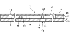
以下、図面を参照しながら本発明のマイクロポンプの好ましい実施態様について具体的に例証する。図1は本発明のマイクロポンプの一例の概要平面図である。本発明のマイクロポンプは例えば、マイクロチップ1などに配設される。マイクロポンプは、基本的に、微細流路7と、該微細流路の途中に配設された2枚の対向片からなる逆止弁9と、加圧部11と、バルブ部13とからなる。微細流路7の一端には少なくとも1個の、液体試薬を注入するための大気に開放されたポート15を有する。また、微細流路7の他端には、必要に応じて少なくとも1個の液体又は気体排出用のポート17を有する。しかし、加圧部11から発生された圧力を抜くことができれば、必ずしもポートという形態である必要はなく、他の形態のものでもよい。なお、図1に示されるようなマイクロチップ自体は特許文献1の図4に記載された方法により製造することができる。
Hereinafter, preferred embodiments of the micropump of the present invention will be specifically illustrated with reference to the drawings. FIG. 1 is a schematic plan view of an example of the micropump of the present invention. The micropump of the present invention is disposed, for example, on the
図2は、図1におけるII-II線に沿った断面図である。本発明のマイクロバルブが配設されるマイクロチップ1は例えば、ガラス又はPDMSからなる対面基板19を有する。対面基板19の上面にはPDMSからなる薄膜21が恒久接着されている。薄膜21の上面には微細流路7などを構成するためのPDMS層23が恒久接着されている。更に、PDMS層23の上面にはPDMSからなる薄膜25が恒久接着されており、この薄膜25の上面には最上層を形成するPDMS層27が恒久接着されている。本発明のマイクロチップ1において2枚のPDMS薄膜21と25を使用するのはバルブ部13を構成するためである。従って、微細流路7、逆止弁9,加圧部11及びバルブ部13は2枚のPDMS薄膜21と25との間に形成されている。言うまでもなく、ポート15及びポート17(もし存在すれば)の部分の薄膜25は除去されている。
FIG. 2 is a cross-sectional view taken along the line II-II in FIG. The
薄膜21及び/又は25の膜厚は一般的に、5μm〜200μmの範囲内であることが好ましい。薄膜21及び/又は25の膜厚が5μm未満では膜の機械的強度が弱すぎて破れてしまう危険性がある。一方、薄膜21及び/又は25の膜厚が200μm超では、膜の機械的強度が高くなりすぎ、膜が撓まなくなる可能性がある。
The film thickness of the
逆止弁9は例えば、互いに擦れ違うように対向する2枚の流路幅よりも短い堰板29と31により構成されている。堰板31はポート15の方向には動くことができないが、加圧部11の方向には動くことが出来る。堰板31を可動性にするため、堰板29よりも薄いことが好ましい。
The
加圧部11は、人の指又は細い棒あるいは機械的手段(例えば、ピエゾ素子などのような圧電素子等)などで押したときに大きな加圧力を発生できるようにするため、微細流路7よりも大きな容積になるように形成することが好ましい。
The pressurizing
バルブ部13では、2枚のPDMS薄膜21と25との間に弁座33が配設されている。薄膜21及び25は弁座33の下面及び上面にそれぞれ離着することができる。PDMS層19及び27において、バルブ部13に対応する位置の部分が切除され、空所35及び37が形成されている。
In the
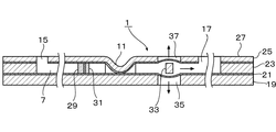
図3は本発明のマイクロバルブの駆動原理を説明する概念図である。ポート15から液体を注入すると、逆止弁9の堰板31がバルブ部13方向に向かって変形することにより、注入液体は逆止弁9とバルブ部13とにより形成される空間内に貯留される。ポート15から圧力を加えて液体を注入しても、逆止弁9とバルブ部13とにより画成される空間内に液体が充満されるまでバルブ部13には変形圧力は加わらない。所定量の液体が逆止弁9とバルブ部13とにより画成される空間内に注入された時点で、ポート15からの注入を停止する。その後、加圧部11の上面を指又は細い棒あるいは機械的手段で押し下げると、正圧が発生し、これにより、逆止弁9の堰板31が他方の堰板29に押し付けられ、一方、薄膜21及び25は弁座33から離れるように空所35及び37に向かってそれぞれ膨張される。その結果、薄膜21及び25と弁座33との間に隙間が生じ、この隙間を通して液体はポート17方向に向かって押し出される。加圧部11の押圧量が一定であれば、バルブ部13を通して送出される液体量も大体一定になる。
FIG. 3 is a conceptual diagram illustrating the driving principle of the microvalve of the present invention. When liquid is injected from the
図4は逆止弁9の別の実施態様を示す部分概要断面図である。図4の実施態様では、堰板29a及び堰板31aが互いに上下に擦れ違うように対向するように配設されている。上流のポート15から液体が注入されると、堰板31aは下流方向に撓み変形して液体を通すことができる。一方、加圧部11が押圧されると、堰板31aは堰板29aに押し付けられ、液体が上流側に流れることは阻止される。堰板29aは圧力を受けても撓み変形することはない。
FIG. 4 is a partial schematic sectional view showing another embodiment of the
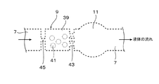
図5は逆止弁9の更に別の実施態様を示す部分概要平面図である。図5の逆止弁9では、弁室39内に複数個のビーズ41が収容されている。弁室39と微細流路7とは、微細流路7の流路幅よりも狭く、かつ、ビーズ41の外径よりも小さい1本以上の接続流路により連通されている。弁室39と加圧部11側との間の接続流路43はビーズ41により閉塞されないように複数本の細い管路で構成することが好ましい。一方、弁室39とポート15側との間の接続流路45はビーズ41により閉塞されやすいように、ビーズ41の外径よりも極僅かに小さな幅を有する1本の管路で構成することが好ましい。弁室39内にビーズ41を充填する場合、図2に示されるPDMS薄膜25を恒久接着させる前に、所定の個数のビーズ41を弁室39に充填し、その後、PDMS薄膜25をPDMS層23に恒久接着させることにより、ビーズ41を弁室39内に誘導可能に閉じ込めることができる。
FIG. 5 is a partial schematic plan view showing still another embodiment of the
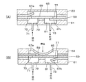
図6は本発明のマイクロポンプの別の実施態様のマイクロチップ1Aの部分概要断面図である。図6のマイクロポンプは2個の逆止弁を使用することによりポンプ吐出機能を実現している。第1の逆止弁47は図4に示された逆止弁9と概ね同じものである。第2の逆止弁49は構造的には第1の逆止弁47と概ね同一である。第1の逆止弁47では、堰板51a及び堰板53aが互いに上下に擦れ違うように対向するように配設されている。堰板51aは圧力を受けても撓み変形しないが、堰板53aは圧力を受けると撓み変形し、堰板51aとの間に隙間を発生させる。第2の逆止弁49では、堰板51b及び堰板53bが互いに上下に擦れ違うように対向するように配設されている。堰板51bは圧力を受けても撓み変形しないが、堰板53bは圧力を受けると撓み変形し、堰板51bとの間に隙間を発生させる。図6に示されたマイクロチップ1Aでは、ガラス又はPDMS基板19の上面に、堰板51a及び51bが立設されているPDMS層55が恒久接着されている。また、このPDMS層55の上面には、微細流路7と、ポート15及び17と、堰板53a及び53bを有するPDMS層57が恒久接着されている。
FIG. 6 is a partial schematic cross-sectional view of a
図7は図6に示されたマイクロチップ1Aにおけるマイクロポンプの駆動原理を説明する部分概要断面図である。図7(A)において、ポートから液体を注入すると、逆止弁47の堰板53aが加圧部11方向に向かって変形することにより、注入液体は逆止弁47と49とにより画成される空間内に貯留される。次いで、図7(B)において、加圧部11の上部外面を指又は細い棒あるいは機械的手段で押し下げると、正圧が発生し、これにより、逆止弁47の堰板53aが他方の堰板51aに押し付けられて閉止されると共に、逆止弁49の堰板53bは圧力を受けて撓み変形し、堰板51bとの間に隙間が発生し、液体はポート17方向に向かって押し出される。
FIG. 7 is a partial schematic cross-sectional view for explaining the driving principle of the micropump in the
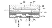
図8は本発明によるマイクロポンプの更に別の実施態様の部分概要断面図である。図8のマイクロポンプは、弁座となるガラス板59の下部のPDMS半型61と上部のPDMS半型63とを重ね合わせることにより密閉されたポンプ室65を画成する。上部のPDMS半型63には圧力により撓み変形することができるPDMS弁片67がスペーサ69を介して配設されている。スペーサ69はPDMSから形成されていることが好ましい。スペーサ69の存在により、PDMS弁片67はガラス板59から離されている。送入管71はPDMS半型61に設けられた送入穴に連結されており、同様に吐出管73もPDMS半型61に設けられた吐出穴に連結されている。送入管71から弁室65内に液体を圧力注入するか又は吸込注入する。吐出管73は細いので弁室65内に貯留された液体はそのままではポンプ外には排出されない。
FIG. 8 is a partial schematic cross-sectional view of still another embodiment of a micropump according to the present invention. The micro pump shown in FIG. 8 defines a sealed
図9に示されるように、PDMS半型63の上面を押圧すると、PDMS弁片67は弁座のガラス板59に密着され、ガラス板59の入口孔75は閉じられる。その結果、弁室65内の液体はガラス板59の出口孔77から吐出管73を介してポンプ外へ吐出される。
As shown in FIG. 9, when the upper surface of the
図10は本発明によるマイクロポンプの更に他の実施態様の部分概要断面図である。図10のマイクロポンプは、ガラス板59の下部のPDMS下側半型61と上部のPDMS上側半型63とを重ね合わせることにより密閉されたポンプ室65を画成する点では図8のマイクロポンプと同じである。図10のマイクロポンプでは、圧力により撓み変形することができるPDMS弁片67aと67bがスペーサを介することなく、配設されている点で図8のマイクロポンプと異なる。PDMS弁片67aはPDMS上側半型63側に配設され、PDMS弁片67bはPDMS下側半型61側に配設されている。PDMS弁片67aはガラス板の入口孔75を密閉し、PDMS弁片67bはガラス板の出口孔77を密閉する。
FIG. 10 is a partial schematic cross-sectional view of still another embodiment of the micropump according to the present invention. The micropump shown in FIG. 10 is different from the micropump shown in FIG. 8 in that a sealed
図11は図10に示されるマイクロポンプの駆動状態を説明する概念図である。図11(A)に示されるように、送入管71から液体を吸込空気室79に圧力注入すると、PDMS弁片67aは撓み変形して、ガラス板の入口孔75との間に隙間を発生し、この隙間から液体がポンプ室65内に貯留される。次いで、図11(B)に示されるように、PDMS上側半型63の上面を押圧すると、PDMS弁片67aはガラス板59に密着され、ガラス板59の入口孔75は閉じられ、同時に、PDMS弁片67bはガラス板59から離されて出口孔77が開放するので、液体は吐出空気室81に送り出され、次いで、吐出管73を介してポンプ外へ吐出される。押圧力を解除すると、負圧が発生するので、図11(A)と同じ状態が生起するので、再びポンプ室65内に液体が吸込注入される。これにより、マイクロポンプとして連続的に液体の吸込・吐出が繰り返される。
FIG. 11 is a conceptual diagram illustrating the driving state of the micropump shown in FIG. As shown in FIG. 11 (A), when liquid is injected from the
図10のマイクロポンプでは、PDMS半型63の上面を人為的に押圧しなければポンプとして駆動させることができない。図12に示されるように、PDMS上側半型63のポンプ室65の上部に、PDMS製のダイヤフラム弁83を配設し、このダイヤフラム弁83を圧電素子85で上下に振動させることによりポンプ室65内に正圧と負圧を交互に発生させ、ポンプとしての吸込・吐出動作を自動的かつ連続的に行うことができる。
The micro pump shown in FIG. 10 cannot be driven as a pump unless the upper surface of the
以上、本発明の好ましい実施態様について説明してきたが、本発明は図示された実施態様のみに限定されない。例えば、流路7に連通する入力ポート15は1個だけでなく、2個以上存在することができ、また、マイクロバルブ13の流体送出先は送出されてきた流体を必要とする部位であるば何でも良い。更に、出力ポート17は必ずしも存在しなくてもよく、必要であれば、1個だけでなく2個以上存在することもできる。従って、本発明のマイクロポンプ機構は流体を送出する必要がある箇所ならばどこででも使用できる。
また、本発明のマイクロポンプ機構はマイクロチップだけでなく、様々な分野における微量流体制御機構で使用することもできる。
Although preferred embodiments of the present invention have been described above, the present invention is not limited to only the illustrated embodiments. For example, there may be not only one
The micropump mechanism of the present invention can be used not only for microchips but also for microfluidic control mechanisms in various fields.
1 本発明のマイクロチップ
7 微細流路
9 逆止弁
11 加圧部
13 マイクロバルブ
15 入力ポート
17 出力ポート
19 対面基板
21,25 PDMS薄膜
23,27 PDMS基板
29,29a,31,31a PDMS堰板
33 弁座
35,37 空所
39 弁室
41 ビーズ
43,45 接続流路
47,49 逆止弁
51a,51b,53a,53b 堰板
55,57 PDMS基板
59 ガラス板
61 PDMS下側半型
63 PDMS上側半型
65 ポンプ室
67 PDMS弁片
69 スペーサ
71 送入管
73 吐出管
75 入口孔
77 出口孔
79 吸込空気室
81 吐出空気室
83 PDMSダイヤフラム弁
85 圧電素子
DESCRIPTION OF
17
Claims (4)
前記対面基板の貼り合わせ面及び第1の基板の上面にポリジメチルシロキサン(PDMS)の薄膜が接着されており、前記第1の基板の上面のPDMS薄膜上に第2の基板が更に接着されており、
前記微細流路内において、前記2枚の薄膜間に、逆止弁と、加圧部と、マイクロバルブが、流体の流れる方向に沿ってこの順に形成されており、
前記加圧部は前記微細流路よりも大きな容積を有する空間であり、
前記マイクロバルブは、前記微細流路の幅及び高さと同じ幅及び高さを有する弁座と該弁座の上面及び下面にそれぞれ離着する各PDMS薄膜からなり、
前記弁座の配設位置に対応する第2の基板及び対面基板の箇所が所定の大きさで切除されていることを特徴とするマイクロチップ。 In a microchip comprising at least a first substrate on which a fine channel is formed and a facing substrate bonded to the fine channel forming surface of the first substrate,
A thin film of polydimethylsiloxane (PDMS) is bonded to the bonding surface of the facing substrate and the upper surface of the first substrate, and a second substrate is further bonded to the PDMS thin film on the upper surface of the first substrate. And
In the fine flow path, a check valve, a pressurizing part, and a micro valve are formed in this order along the fluid flow direction between the two thin films,
The pressurizing part is a space having a larger volume than the fine channel,
The microvalve comprises a valve seat having the same width and height as the width and height of the fine flow path, and each PDMS thin film attached to and detached from the upper and lower surfaces of the valve seat,
2. The microchip according to claim 1, wherein a portion of the second substrate and the facing substrate corresponding to the position where the valve seat is disposed is cut out to a predetermined size.
Priority Applications (1)
| Application Number | Priority Date | Filing Date | Title |
|---|---|---|---|
| JP2004097638A JP4403000B2 (en) | 2004-03-30 | 2004-03-30 | Microchip and micropump |
Applications Claiming Priority (1)
| Application Number | Priority Date | Filing Date | Title |
|---|---|---|---|
| JP2004097638A JP4403000B2 (en) | 2004-03-30 | 2004-03-30 | Microchip and micropump |
Publications (3)
| Publication Number | Publication Date |
|---|---|
| JP2005283331A JP2005283331A (en) | 2005-10-13 |
| JP2005283331A5 JP2005283331A5 (en) | 2007-03-29 |
| JP4403000B2 true JP4403000B2 (en) | 2010-01-20 |
Family
ID=35181884
Family Applications (1)
| Application Number | Title | Priority Date | Filing Date |
|---|---|---|---|
| JP2004097638A Expired - Fee Related JP4403000B2 (en) | 2004-03-30 | 2004-03-30 | Microchip and micropump |
Country Status (1)
| Country | Link |
|---|---|
| JP (1) | JP4403000B2 (en) |
Cited By (1)
| Publication number | Priority date | Publication date | Assignee | Title |
|---|---|---|---|---|
| JP2019063981A (en) * | 2017-09-29 | 2019-04-25 | 研能科技股▲ふん▼有限公司 | Fluid system |
Families Citing this family (25)
| Publication number | Priority date | Publication date | Assignee | Title |
|---|---|---|---|---|
| DE102005052752A1 (en) * | 2005-11-04 | 2007-05-10 | Clondiag Chip Technologies Gmbh | Apparatus and method for detecting molecular interactions |
| KR100691732B1 (en) | 2006-02-22 | 2007-03-12 | 재단법인서울대학교산학협력재단 | Method for manufacturing three dimensional pdms structure |
| JP4793442B2 (en) | 2006-03-29 | 2011-10-12 | 株式会社村田製作所 | Micro pump |
| TW200833950A (en) * | 2007-02-09 | 2008-08-16 | Cooler Master Co Ltd | A thin film pump |
| WO2008108481A1 (en) * | 2007-03-05 | 2008-09-12 | Nec Corporation | Flow control mechanism for microchip |
| JP5532218B2 (en) * | 2007-09-10 | 2014-06-25 | 日本電気株式会社 | Sample filling device |
| JP5228797B2 (en) * | 2008-10-28 | 2013-07-03 | 藤倉化成株式会社 | Liquid channel device |
| US9579653B2 (en) | 2008-06-26 | 2017-02-28 | Fujikura Kasei Co., Ltd. | Liquid channel device and production method therefor |
| CN103341369B (en) | 2008-10-28 | 2015-04-29 | 藤仓化成株式会社 | Liquid passage device and manufacturing method |
| JP5402262B2 (en) * | 2009-06-05 | 2014-01-29 | 株式会社リコー | Microvalve and manufacturing method thereof |
| JP5428624B2 (en) * | 2009-08-03 | 2014-02-26 | 株式会社リコー | Microvalve and manufacturing method thereof |
| JP2011232223A (en) * | 2010-04-28 | 2011-11-17 | Power Supply Kk | Microchannel plate |
| DE102011003856B4 (en) | 2011-02-09 | 2020-06-18 | Robert Bosch Gmbh | Microsystem for fluidic applications as well as manufacturing and use methods for a microsystem for fluidic applications |
| JP6172711B2 (en) | 2012-07-05 | 2017-08-02 | 国立研究開発法人理化学研究所 | Fluid control device for microchip and use thereof |
| WO2014091334A2 (en) * | 2012-12-13 | 2014-06-19 | Koninklijke Philips N.V. | Fluidic system with fluidic stop. |
| CN105452659B (en) * | 2013-08-12 | 2018-08-17 | 皇家飞利浦有限公司 | Has valvular microfluidic device |
| BR112016022867A2 (en) | 2014-04-25 | 2018-07-03 | Hewlett Packard Development Co | diagnostic cassette. |
| JP5866470B1 (en) * | 2015-05-01 | 2016-02-17 | 株式会社朝日Fr研究所 | Check valve and microchemical chip using the same |
| KR101768040B1 (en) * | 2016-07-29 | 2017-08-14 | 한국과학기술원 | A valve for lap-on-a-chip |
| KR101824246B1 (en) * | 2017-03-21 | 2018-01-31 | 재단법인 대구경북과학기술원 | Selective bonding method of polymer materials |
| KR101888376B1 (en) * | 2017-05-12 | 2018-08-14 | 티엔에스(주) | Gene chip for diagnosing infectious diseases |
| KR101910818B1 (en) | 2017-06-02 | 2018-10-30 | 대한민국 | A lap-on-a-chip for genetic testing |
| JP2019002926A (en) * | 2017-06-19 | 2019-01-10 | 積水化学工業株式会社 | Microfluidic device and method for feeding fluid |
| CN108204355A (en) * | 2018-01-12 | 2018-06-26 | 长春工业大学 | A kind of 3 points of clamped membrane valve piezoelectric pumps |
| JP7214500B2 (en) * | 2019-02-20 | 2023-01-30 | 東芝テック株式会社 | Piezoelectric pump and liquid ejection device |
-
2004
- 2004-03-30 JP JP2004097638A patent/JP4403000B2/en not_active Expired - Fee Related
Cited By (2)
| Publication number | Priority date | Publication date | Assignee | Title |
|---|---|---|---|---|
| JP2019063981A (en) * | 2017-09-29 | 2019-04-25 | 研能科技股▲ふん▼有限公司 | Fluid system |
| JP7030655B2 (en) | 2017-09-29 | 2022-03-07 | 研能科技股▲ふん▼有限公司 | Fluid system |
Also Published As
| Publication number | Publication date |
|---|---|
| JP2005283331A (en) | 2005-10-13 |
Similar Documents
| Publication | Publication Date | Title |
|---|---|---|
| JP4403000B2 (en) | Microchip and micropump | |
| US8092761B2 (en) | Mechanically-actuated microfluidic diaphragm valve | |
| US7892496B2 (en) | Mechanically-actuated microfluidic pinch valve | |
| JP4372616B2 (en) | Microvalve, micropump and microchip incorporating them | |
| KR100509254B1 (en) | Micro-fluidic device to control flow time of micro-fluid | |
| US7842248B2 (en) | Microfluidic system comprising microfluidic pump, mixer or valve | |
| US8080220B2 (en) | Thermal bend actuated microfluidic peristaltic pump | |
| US8062612B2 (en) | MEMS integrated circuit comprising microfluidic diaphragm valve | |
| WO2006123578A1 (en) | Testing chip for analyzing target substance contained in analyte, and microscopic comprehensive analytical system | |
| KR100618320B1 (en) | An apparatus for making a fluid flow, and a disposable chip having the same | |
| JPWO2009008236A1 (en) | Micro inspection chip liquid mixing method and inspection apparatus | |
| US8075855B2 (en) | MEMS integrated circuit comprising peristaltic microfluidic pump | |
| US7981386B2 (en) | Mechanically-actuated microfluidic valve | |
| JP5104316B2 (en) | Passive one-way valve and microfluidic device | |
| US20090314368A1 (en) | Microfluidic System Comprising Pinch Valve and On-Chip MEMS Pump | |
| JP2007322284A (en) | Microchip and filling method of reagent in microchip | |
| JP2006053064A (en) | Micro-fluid chip and its manufacturing method | |
| US7887756B2 (en) | Microfluidic system comprising mechanically-actuated microfluidic pinch valve | |
| US20090317302A1 (en) | Microfluidic System Comprising MEMS Integrated Circuit | |
| WO2010092845A1 (en) | Micro-flow passage structure and micropump | |
| JP3905074B2 (en) | Microfluidic control mechanism and microchip having the mechanism | |
| JP2006029485A (en) | Microvalve and micro fluid device having the same | |
| Moriguchi et al. | Simple bilayer on-chip valves using reversible sealability of PDMS | |
| JP2007248218A (en) | Microchip | |
| JP4934205B2 (en) | Micro valve mechanism |
Legal Events
| Date | Code | Title | Description |
|---|---|---|---|
| A521 | Written amendment |
Free format text: JAPANESE INTERMEDIATE CODE: A523 Effective date: 20070207 Free format text: JAPANESE INTERMEDIATE CODE: A821 Effective date: 20070207 |
|
| A621 | Written request for application examination |
Free format text: JAPANESE INTERMEDIATE CODE: A621 Effective date: 20070207 |
|
| A711 | Notification of change in applicant |
Free format text: JAPANESE INTERMEDIATE CODE: A712 Effective date: 20080424 |
|
| A977 | Report on retrieval |
Free format text: JAPANESE INTERMEDIATE CODE: A971007 Effective date: 20090428 |
|
| A131 | Notification of reasons for refusal |
Free format text: JAPANESE INTERMEDIATE CODE: A131 Effective date: 20090818 |
|
| A521 | Written amendment |
Free format text: JAPANESE INTERMEDIATE CODE: A523 Effective date: 20090930 Free format text: JAPANESE INTERMEDIATE CODE: A821 Effective date: 20090930 |
|
| TRDD | Decision of grant or rejection written | ||
| A01 | Written decision to grant a patent or to grant a registration (utility model) |
Free format text: JAPANESE INTERMEDIATE CODE: A01 Effective date: 20091027 |
|
| A01 | Written decision to grant a patent or to grant a registration (utility model) |
Free format text: JAPANESE INTERMEDIATE CODE: A01 |
|
| A61 | First payment of annual fees (during grant procedure) |
Free format text: JAPANESE INTERMEDIATE CODE: A61 Effective date: 20091030 |
|
| R150 | Certificate of patent or registration of utility model |
Free format text: JAPANESE INTERMEDIATE CODE: R150 |
|
| FPAY | Renewal fee payment (event date is renewal date of database) |
Free format text: PAYMENT UNTIL: 20121106 Year of fee payment: 3 |
|
| FPAY | Renewal fee payment (event date is renewal date of database) |
Free format text: PAYMENT UNTIL: 20121106 Year of fee payment: 3 |
|
| FPAY | Renewal fee payment (event date is renewal date of database) |
Free format text: PAYMENT UNTIL: 20151106 Year of fee payment: 6 |
|
| R250 | Receipt of annual fees |
Free format text: JAPANESE INTERMEDIATE CODE: R250 |
|
| R250 | Receipt of annual fees |
Free format text: JAPANESE INTERMEDIATE CODE: R250 |
|
| R250 | Receipt of annual fees |
Free format text: JAPANESE INTERMEDIATE CODE: R250 |
|
| S531 | Written request for registration of change of domicile |
Free format text: JAPANESE INTERMEDIATE CODE: R313531 |
|
| R350 | Written notification of registration of transfer |
Free format text: JAPANESE INTERMEDIATE CODE: R350 |
|
| LAPS | Cancellation because of no payment of annual fees |