JP4399755B2 - High frequency switch module - Google Patents
High frequency switch module Download PDFInfo
- Publication number
- JP4399755B2 JP4399755B2 JP2000173257A JP2000173257A JP4399755B2 JP 4399755 B2 JP4399755 B2 JP 4399755B2 JP 2000173257 A JP2000173257 A JP 2000173257A JP 2000173257 A JP2000173257 A JP 2000173257A JP 4399755 B2 JP4399755 B2 JP 4399755B2
- Authority
- JP
- Japan
- Prior art keywords
- switch module
- frequency switch
- metal case
- laminate
- terminal
- Prior art date
- Legal status (The legal status is an assumption and is not a legal conclusion. Google has not performed a legal analysis and makes no representation as to the accuracy of the status listed.)
- Expired - Lifetime
Links
Images


Landscapes
- Waveguide Connection Structure (AREA)
- Surface Acoustic Wave Elements And Circuit Networks Thereof (AREA)
- Transceivers (AREA)
Description
【0001】
【産業上の利用分野】
本発明は、通過帯域の異なる複数の送受信系を取り扱うマルチバンド用高周波スイッチモジュールに関し、特に積層体上に搭載されたチップ素子や高周波機能部品を包囲する金属ケースの構造に関するものである。
【0002】
【従来の技術】
近年の携帯電話の普及には、目を見張るものがあり、携帯電話の機能、サービスの向上が図られている。この新たな携帯電話として、デュアルバンドあるいはトリプルバンド携帯電話の提案がなされている。これらの携帯電話は、2つあるいは3つの送受信系を取り扱うもので、それぞれ周波数に応じた信号経路、及び複数の周波数を切り換えるためのスイッチとして、分波回路とスイッチ回路を用いて構成される高周波スイッチモジュールが用いられている。
【0003】
例えば、特開平11−225088号公報に開示された高周波スイッチモジュールは、小型化を図るために分波回路、ローパスフィルタ回路及びスイッチ回路の伝送線路を誘電体層内に構成し、一体燒結した積層体(以下、単に積層体と言う。)となし、ダイオード、チップコンデンサ等のチップ素子を前記積層体上に搭載したワンチップ化構造のものである。また、面実装が可能なように各端子電極やグランド端子は、図7に示すように積層体80の各側面に形成され、さらに上面まで延出してランド81、82…が設けられている。そして、チップ素子等の搭載部品を包囲して主に電磁波シールドの働きをなす金属ケース90は、積層体上面のグランド端子のランド82に半田付けで固定されていた。
【0004】
【発明が解決しようとする課題】
このような高周波モジュールにおいては、さらなる機能の集積化が進められており、例えば、従来、上記高周波モジュールの後段に配置されていたバンドパスフィルタ回路をワンチップの積層体に集約することが提案されている。このバンドパスフィルタ回路として現状では、専らパッケージ化された弾性表面波素子(SAW)が用いられており、具体的には2個ないし3個のSAWフィルタを積層体上面に搭載することになる。しかしこの場合でも積層体の面積(搭載有効面積)は、従来と同等であることが望まれるので、チップ素子は極めて厳しい配置構成を余儀なくされる。例えば、図7に示したモジュールでは積層体の上面のランドに金属ケースを固定する構造としていたが、このような構造であるとランドとチップ素子との距離が近づき過ぎてしまい半田ブリッジによる短絡の恐れもあるし、電磁界的な干渉が生じて高周波特性が劣化すると言う問題が生じる。このような問題は更なる小型化が望まれる将来において顕著になると考えられる。
【0005】
また、従来のグランド端子のランドは各送受信系の端子を挟む形で間隔をおいて設けられていた。従って、金属ケース先端83、84、85、86…を断続的に接触させて半田付けしていたので、金属ケースの位置が多少ズレることがあった。また接触面積が十分とれずアース電流の経路が不安定になったり、電磁界の分布が変化して高周波特性が変化することがある。特に、マイクロ波やミリ波帯等の高周波帯域においてはその影響が顕著となる。
また、パッケージ型SAWフィルタを搭載すると低背化を阻害するし、もともとSAWフィルタは外力や温度変化に対して繊細であることから、パッケージの廻りには空間を保っていることが望ましい。
【0006】
以上のことより本発明は、チップ素子やSAWフィルタを搭載した高周波モジュールにおいて、積層体の搭載有効面積を最大限利用して尚かつ低背化をはかり、このとき、チップ素子と端子間の干渉を低減し、また、SAWフィルタを外的に保護しアースを確実にとるようになした高周波スイッチモジュールを提供することを目的とする。
【0007】
【課題を解決するための手段】
本発明は、内部に電極パターンで伝送線路やコンデンサを形成した積層体の主面に搭載部品を実装するとともに、前記搭載部品を覆う金属ケースを配置して、フィルタ回路やスイッチ回路を構成した高周波スイッチモジュールであって、前記積層体は側面電極を備えず、前記積層体の主面には、グランド端子と、搭載部品が実装されるランドが設けられるとともに、前記金属ケースが前記主面上に搭載されて前記グランド端子と接続し、前記金属ケースは、天板と前記天板から積層体の主面側に突き出た突出部と、近接する搭載部品との短絡を防ぐ開口部を備え、前記突出部を前記グランド端子とはんだ接続したことを特徴とする。
本発明においては、前記金属ケースの開口部側に設けられたランドを、突出部側のランドと比べて、積層体側面の近傍にまで形成するのが好ましい。また、積層体の内部電極パターンと、主面に実装されたチップ素子と、前記積層体の底面に設けられた端子電極とは、全て積層体に形成されたスルーホールを介して接続されるのが好ましい。
前記積層体の底面側の内層には、そのほぼ全面にグランド電極が形成されており、スルーホールを介して前記金属ケースと接続する。
【0008】
以上により、グランド端子以外の端子は積層体上面に設けていないのでチップ素子等との干渉の問題がなく高周波特性が安定する。また、金属ケースの一端はグランド端子に面接触しアースが充分にとれて電流の経路も安定する。一方、SAWフィルタ側の他端は開口しておりSAWフィルタの廻りに空間が形成され、外力や温度に対する影響を受けることがなくなる。また、外見上ケースを見てモジュールの方向性を識別できるので、例えば基板上への組立てに間違いがなくなる。
【0009】
尚、上記の各回路構成において、分波回路はLC回路で構成され、スイッチ回路はダイオードと伝送線路を主構成とし、フィルタ回路はSAWフィルタで構成され、整合回路はコンデンサ又はLC回路で構成され、また分波回路のLC回路及びスイッチ回路の伝送線路は、誘電体による積層体内に電極パターンにより構成することが望ましい。
【0010】
【発明の実施の形態】
以下、本発明の一実施例を図面を参照して説明する。
図1〜図5は一実施例の高周波スイッチモジュールを示し、図1は積層体に金属ケースを装着した斜視図である。図2は側面から見た一部断面図である。図3は実施例の積層体を示す斜視図である。図4は前記積層体の裏面を示す平面図である。図5は前記積層体にチップ素子やSAWフィルタを搭載した状態を示す斜視図である。図6は積層体の内部構造図の一例を示すグリーンシートの展開図である。
【0011】
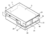
本実施例は、第1の送受信系としてEGSM900(Extended Global System for Mobile Communications 900)方式を、第2の送受信系としてGSM1800方式を用いるもので、この2つの送受信系に信号を分波する分波回路と、各送受信系のそれぞれに送信系と受信系を切り換えるスイッチ回路と、このスイッチ回路の各受信系の特定の信号を通過させるフィルタ回路と、スイッチ回路とフィルタ回路の整合回路とを、ワンチップの積層体に集積したデュアルバンド用高周波スイッチモジュールを例にとる。この高周波スイッチモジュール1は、下記で若干説明するように分波回路、ローパスフィルタ回路及びスイッチ回路の伝送線路を積層体内に構成し、他方、ダイオード、チップコンデンサ及びSAWフィルタを積層体上面に搭載して構成している。また、SAWフィルタ等の搭載部品を覆う金属ケース3を備えている。
【0012】
先ず、積層体2の内部構造について簡単に説明する。この積層体2は低温焼成が可能なセラミック誘電体材料からなるグリーンシートを用意し、この上に通常Agを主体とする導電ペーストを印刷して所望の電極パターンを形成する。尚、この電極パターンと同じものをシート上に並列に複数個形成している。このようなシートを適宜積層して熱圧着した後、チップ状に切断する。そしてこのチップを一体燒結して積層体2を得ている。
【0013】
積層体2の内部構造は図6に示すように▲2▼から(18)(10以上の数値はカッコを付す。)までのグリーンシートを、▲2▼を最下層とし以後順に積層したものである。尚、グリーンシート▲1▼は▲2▼の裏面を示している。一番下層のグリーンシート▲2▼にはほぼ全面にグランド電極61が形成されており、その裏面23には複数のスルーホール63を介して細長いグランド端子60が左右に形成されている。他の端子は、図4に示すように長手方向側面にGSM1800系の送信TX端子51、電圧VC1端子52、グランド端子53、電圧VC2端子54、GSM1800系の受信RX端子55がそれぞれ設けられている。また、対向する上部にはEGSM900系の受信RX端子57、グランド端子58、共通のアンテナ端子59、グランド端子60、EGSM900系の送信TX端子61がそれぞれ形成されている。これらの端子電極は半田電極を介して基板に実装することになる。
また、グリーンシートの向かって左側端(チップ素子を搭載する側)のスルーホール63は、その上に重なる全てのグリーンシートにも複数個のスルーホール63(符号省略)が設けられており、最上層のグリーンシート(18)にはスルーホール63を介して細長いグランド端子66が形成されている。
【0014】
次に、コンデンサ用の電極62が複数形成されたグリーンシート▲3▼、その上にグランド電極61が形成されたグリーンシート▲4▼が積層される。さらにその上のグリーンシート▲5▼、▲6▼、▲7▼、▲8▼、▲9▼、(10)にはそれぞれ適宜ライン電極64、コンデンサ電極62、スルーホール(符号省略、以下他電極の符号も省略する。)が形成されており、概略グリーンシートの上側にEGSM900系の伝送線路やコンデンサを配置し、下側にGSM1800系の伝送線路やコンデンサを配置している。そして、グリーンシート▲4▼、▲5▼、▲6▼、▲7▼、▲8▼、▲9▼、(10)で略ローパスフィルタ回路を構成し、グリーンシート▲2▼、▲3▼、▲4▼、▲5▼、▲6▼、▲7▼、▲8▼、▲9▼、(10)でスイッチ回路を構成している。
【0015】
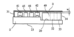
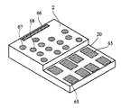
次に、グリーンシート(11)から上には左側にコンデンサ電極やライン電極を、右側にSAWフィルタのランド接続部が形成される。グリーンシート(11)、(12)、(13)、(14)、(15)、(16)でほぼ分波回路を構成し、グリーンシート(17)には配線パターンが形成され、最上層のグリーンシート(18)にはダイオード及びチップコンデンサ用のランド接続部およびグランド端子66が形成されている。その外観は図3に示すようで、積層体の上面の左側にはダイオード接続用の一対のランド67と、チップコンデンサ接続用の一対のランド68が形成され、右側には段差部20が設けられており、SAWフィルタ接続用のランド65が4個づつ並列に形成されている。
【0016】
図5は積層体2の上面にそれぞれチップ素子やSAWフィルタを搭載した状況を示している。即ち、上記したそれぞれ一対のランドに対し、ダイオード41、42、43、44とチップ抵抗45、チップコンデンサ46、47を半田付けし、また、段差部20のランド上にパッケージ型SAWフィルタ48、49を半田付けで載置している。この積層体の外形寸法は約6.6×4.9×0.9mmと極小さく、積層体上面の搭載有効面積には余裕がない。そこで、側面端子のランドは無くし、かつチップ素子間の間隙も必要最小限とし密度の高い配置とした。また、高さ方向もチップ素子との高さとバランスするようにSAWフィルタは段差部20上に設けるようになし低背化を図っている。
【0017】
次に、これらの搭載部品を包囲する金属ケース3は、一端に幅広の略T字状の突出部31を有し、この突出部31は積層体上面のグランド端子66上に当接し半田付けで固定される。また、ケースの他端側は開口34されており、その側面側に一対の突出部32、33を有している。この突出部32、33はSAWファイルタの上面に間隙gを確保できるだけの長さに設定されており、段差部20に設けられたSAWファイルタのグランド用のランド上に当接し半田付けで設置される。尚、開口34は多少の壁部分が存在していても良い。これによってSAWフィルタ側のケース端部は開口されているので十分な空間が形成されSAWフィルタの温度特性に影響を及ぼし難く、モジュール本体の方向性も識別できる。尚、金属ケースのアースも確実にとることができ電流経路も安定する。
【0018】
本発明の他の実施例としては、トリプルバンド高周波スイッチモジュールに対しても同様に実施することが出来る。また、SAWフィルタは必ずしもパッケージ型のものを用いる必要はなくベアチップのものを使用することも可能である。
【0019】
【発明の効果】
本発明によれば、積層体上面に側面端子及びそのランドを設けない構成としたのでチップ素子との干渉が低減された。また、金属ケースはアース面積が大きく確実にとれるものとしたのでアースをとることが安定した。また、ケースの一端を開口したので温度による悪影響が抑制された。以上により電気的特性の良い高周波スイッチモジュールを提供することができた。
【図面の簡単な説明】
【図1】本発明に係る高周波スイッチモジュールの一実施例を示し、積層体に金属ケースを装着した斜視図である。
【図2】側面から見た一部断面図である。
【図3】図1の積層体を示す斜視図である。
【図4】積層体の裏面を示す平面図である。
【図5】積層体にチップ素子やSAWフィルタを搭載した後の斜視図である。
【図6】積層体の内部構造図の一例である。
【図7】従来の高周波スイッチモジュールの一例を示す斜視図である。
【符号の説明】
1:高周波スイッチモジュール
2:積層体
3:金属ケース
20:段差部
21、22:積層体の幅方向側面
23:積層体の裏面
24:積層体の長手方向側面
31:金属ケースのT字状の突出部
32、33:金属ケースの対の突出部
34:金属ケースの開口部
41、42、43、44:ダイオード
45:チップ抵抗
46、47:チップコンデンサ
48、49:パッケージ型SAWフィルタ
51〜62:積層体裏面の各端子[0001]
[Industrial application fields]
The present invention relates to a multiband high-frequency switch module that handles a plurality of transmission / reception systems having different passbands, and more particularly to a structure of a metal case surrounding a chip element or a high-frequency functional component mounted on a laminate.
[0002]
[Prior art]
In recent years, the spread of mobile phones has been remarkable, and the functions and services of mobile phones have been improved. As this new mobile phone, a dual-band or triple-band mobile phone has been proposed. These mobile phones handle two or three transmission / reception systems, each of which has a signal path corresponding to the frequency and a high frequency circuit configured by using a branching circuit and a switch circuit as a switch for switching a plurality of frequencies. A switch module is used.
[0003]
For example, a high-frequency switch module disclosed in Japanese Patent Application Laid-Open No. 11-225088 is a laminate in which transmission lines of a demultiplexing circuit, a low-pass filter circuit, and a switch circuit are configured in a dielectric layer and are integrally consolidated in order to reduce the size. And a one-chip structure in which chip elements such as diodes and chip capacitors are mounted on the laminate. Further, each terminal electrode and ground terminal are formed on each side surface of the laminated
[0004]
[Problems to be solved by the invention]
In such a high-frequency module, further integration of functions has been promoted. For example, it has been proposed to consolidate band-pass filter circuits, which have been conventionally arranged at the subsequent stage of the high-frequency module, into a one-chip laminate. ing. Currently, a surface acoustic wave element (SAW) packaged exclusively is used as this band-pass filter circuit. Specifically, two to three SAW filters are mounted on the upper surface of the laminate. However, even in this case, since it is desired that the area of the laminate (mounting effective area) is the same as that of the conventional one, the chip elements are forced to have an extremely strict arrangement configuration. For example, the module shown in FIG. 7 has a structure in which a metal case is fixed to the land on the upper surface of the laminated body. However, with such a structure, the distance between the land and the chip element becomes too close, and a short circuit due to a solder bridge occurs. There is also a fear that there is a problem that high frequency characteristics deteriorate due to electromagnetic interference. Such a problem is likely to become prominent in the future where further miniaturization is desired.
[0005]
Further, the lands of the conventional ground terminal are provided at intervals so as to sandwich the terminals of each transmission / reception system. Therefore, since the
Further, when a package type SAW filter is mounted, the height reduction is hindered, and since the SAW filter is originally sensitive to external force and temperature change, it is desirable to keep a space around the package.
[0006]
As described above, the present invention achieves a reduction in height by making the best use of the effective mounting area of the laminated body in a high-frequency module mounted with a chip element and a SAW filter. It is another object of the present invention to provide a high-frequency switch module that can reduce the noise and protect the SAW filter externally to ensure the grounding.
[0007]
[Means for Solving the Problems]
The present invention is configured with implementing mounted components on the main surface of the product layer body formed of the transmission lines and capacitors in the electrode pattern therein, by placing a metal case covering said mounting component, a filter circuit and the switching circuit a high-frequency switch modules, the laminated body is not provided with the side electrodes, wherein the main surface of the laminate, a ground terminal, Rutotomoni land provided mounting component is mounted, wherein the metal case is the main Mounted on the surface and connected to the ground terminal, the metal case has an opening for preventing a short circuit between the top plate and the projecting portion projecting from the top plate to the main surface side of the laminate, and an adjacent mounting component. And the protrusion is solder-connected to the ground terminal.
In the present invention, it is preferable that the land provided on the opening side of the metal case is formed to the vicinity of the side surface of the laminate as compared with the land on the projecting portion side. In addition, the internal electrode pattern of the multilayer body, the chip element mounted on the main surface, and the terminal electrodes provided on the bottom surface of the multilayer body are all connected through the through holes formed in the multilayer body. Is preferred.
A ground electrode is formed on almost the entire inner layer on the bottom surface side of the laminate, and is connected to the metal case through a through hole.
[0008]
As described above, since terminals other than the ground terminal are not provided on the upper surface of the laminated body, there is no problem of interference with the chip element and the like, and the high frequency characteristics are stabilized. In addition, one end of the metal case is in surface contact with the ground terminal, and the ground is sufficiently taken to stabilize the current path. On the other hand, the other end on the SAW filter side is open, and a space is formed around the SAW filter so that it is not affected by external force or temperature. In addition, since the appearance of the module can be identified by looking at the case, there is no mistake in assembling on the substrate, for example.
[0009]
In each of the circuit configurations described above, the branching circuit is composed of an LC circuit, the switch circuit is composed mainly of a diode and a transmission line, the filter circuit is composed of a SAW filter, and the matching circuit is composed of a capacitor or an LC circuit. Also, it is desirable that the LC circuit of the branching circuit and the transmission line of the switch circuit are configured by electrode patterns in a dielectric laminate.
[0010]
DETAILED DESCRIPTION OF THE INVENTION
Hereinafter, an embodiment of the present invention will be described with reference to the drawings.
1 to 5 show a high-frequency switch module according to an embodiment, and FIG. 1 is a perspective view in which a metal case is mounted on a laminate. FIG. 2 is a partial cross-sectional view seen from the side. FIG. 3 is a perspective view showing the laminate of the example. FIG. 4 is a plan view showing the back surface of the laminate. FIG. 5 is a perspective view showing a state in which chip elements and SAW filters are mounted on the laminate. FIG. 6 is a development view of a green sheet showing an example of the internal structure of the laminate.
[0011]
In this embodiment, an EGSM900 (Extended Global System for Mobile Communications 900) system is used as a first transmission / reception system, and a GSM1800 system is used as a second transmission / reception system. A circuit, a switch circuit that switches between a transmission system and a reception system for each transmission / reception system, a filter circuit that passes a specific signal of each reception system of the switch circuit, and a matching circuit between the switch circuit and the filter circuit. Take a dual-band high-frequency switch module integrated in a chip stack as an example. The high-
[0012]
First, the internal structure of the
[0013]
As shown in Fig. 6, the internal structure of
In addition, the through
[0014]
Next, a green sheet (3) having a plurality of
[0015]
Next, a capacitor electrode and a line electrode are formed on the left side above the green sheet (11), and a land connection part of the SAW filter is formed on the right side. The green sheets (11), (12), (13), (14), (15), and (16) constitute almost the branching circuit, and the wiring pattern is formed on the green sheet (17). The green sheet (18) is formed with land connection portions and
[0016]
FIG. 5 shows a situation in which chip elements and SAW filters are mounted on the upper surface of the
[0017]
Next, the
[0018]
Another embodiment of the present invention can be similarly applied to a triple band high frequency switch module. Further, the SAW filter does not necessarily need to be a package type, and can be a bare chip.
[0019]
【The invention's effect】
According to the present invention, since the side surface terminal and the land thereof are not provided on the upper surface of the laminate, the interference with the chip element is reduced. In addition, since the metal case has a large grounding area and can be taken reliably, it is stable to ground. Moreover, since one end of the case was opened, adverse effects due to temperature were suppressed. As described above, a high-frequency switch module having good electrical characteristics can be provided.
[Brief description of the drawings]
FIG. 1 is a perspective view showing an embodiment of a high-frequency switch module according to the present invention, in which a metal case is mounted on a laminate.
FIG. 2 is a partial cross-sectional view seen from the side.
FIG. 3 is a perspective view showing the laminated body of FIG.
FIG. 4 is a plan view showing the back surface of the laminated body.
FIG. 5 is a perspective view after a chip element and a SAW filter are mounted on the laminate.
FIG. 6 is an example of an internal structure diagram of a laminated body.
FIG. 7 is a perspective view showing an example of a conventional high-frequency switch module.
[Explanation of symbols]
1: High frequency switch module 2: Laminated body 3: Metal case 20: Stepped
Claims (4)
前記積層体は側面電極を備えず、前記積層体の主面には、グランド端子と、搭載部品が実装されるランドが設けられるとともに、前記金属ケースが前記主面上に搭載されて前記グランド端子と接続し、
前記金属ケースは、天板と前記天板から積層体の主面側に突き出た突出部と、近接する搭載部品との短絡を防ぐ開口部を備え、前記突出部を前記グランド端子とはんだ接続したことを特徴とする高周波スイッチモジュール。With implementing mounted components on the main surface of the internal electrode pattern product layer body formed of the transmission lines and capacitors, by placing a metal casing covering the mounting part, the high-frequency switch module configured to filter circuit and the switching circuit Because
The laminated body is not provided with the side electrodes, wherein the main surface of the laminate, a ground terminal and, Rutotomoni land is provided mounting component is mounted, wherein the metal case is mounted on the primary surface ground Connected to the terminal,
The metal case includes a top plate, a protrusion protruding from the top plate toward the main surface of the laminate, and an opening that prevents a short circuit between adjacent mounting components, and the protrusion is solder-connected to the ground terminal. A high-frequency switch module characterized by that.
Priority Applications (1)
| Application Number | Priority Date | Filing Date | Title |
|---|---|---|---|
| JP2000173257A JP4399755B2 (en) | 2000-06-09 | 2000-06-09 | High frequency switch module |
Applications Claiming Priority (1)
| Application Number | Priority Date | Filing Date | Title |
|---|---|---|---|
| JP2000173257A JP4399755B2 (en) | 2000-06-09 | 2000-06-09 | High frequency switch module |
Publications (3)
| Publication Number | Publication Date |
|---|---|
| JP2001352272A JP2001352272A (en) | 2001-12-21 |
| JP2001352272A5 JP2001352272A5 (en) | 2007-07-05 |
| JP4399755B2 true JP4399755B2 (en) | 2010-01-20 |
Family
ID=18675527
Family Applications (1)
| Application Number | Title | Priority Date | Filing Date |
|---|---|---|---|
| JP2000173257A Expired - Lifetime JP4399755B2 (en) | 2000-06-09 | 2000-06-09 | High frequency switch module |
Country Status (1)
| Country | Link |
|---|---|
| JP (1) | JP4399755B2 (en) |
Families Citing this family (3)
| Publication number | Priority date | Publication date | Assignee | Title |
|---|---|---|---|---|
| US6700061B2 (en) | 2000-10-17 | 2004-03-02 | Murata Manufacturing Co., Ltd. | Composite electronic component |
| JP2004235184A (en) | 2003-01-28 | 2004-08-19 | Matsushita Electric Ind Co Ltd | High frequency device |
| KR100880800B1 (en) * | 2005-04-18 | 2009-02-02 | 가부시키가이샤 무라타 세이사쿠쇼 | High frequency module |
-
2000
- 2000-06-09 JP JP2000173257A patent/JP4399755B2/en not_active Expired - Lifetime
Also Published As
| Publication number | Publication date |
|---|---|
| JP2001352272A (en) | 2001-12-21 |
Similar Documents
| Publication | Publication Date | Title |
|---|---|---|
| KR100947943B1 (en) | High frequency power amplifier module | |
| US6456172B1 (en) | Multilayered ceramic RF device | |
| US6252778B1 (en) | Complex electronic component | |
| EP1094538A2 (en) | Multilayered ceramic RF device | |
| KR100697767B1 (en) | Antenna duplexer and electronic device | |
| KR19990062840A (en) | Multiband High Frequency Switching Module | |
| KR100642612B1 (en) | Duplexer device | |
| JP4166635B2 (en) | Multilayer high frequency module | |
| JP3925771B2 (en) | High frequency switch module | |
| JP4399755B2 (en) | High frequency switch module | |
| JP2001352271A (en) | High frequency switch module | |
| JP3514453B1 (en) | High frequency components | |
| JP3838386B2 (en) | Compound switch | |
| JP4596300B2 (en) | High frequency switch module | |
| JP2001352270A (en) | High frequency switch module | |
| JP4114106B2 (en) | Composite switch circuit and composite switch circuit component | |
| JP4177282B2 (en) | Antenna switching module | |
| JP2002158449A (en) | High-frequency electronic circuit module and multilayer board therefor | |
| JP2000049651A (en) | High frequency switch module for multi-band | |
| JP4331634B2 (en) | Antenna switching module and manufacturing method thereof | |
| JP3871156B2 (en) | Composite switch circuit parts | |
| JP4005829B2 (en) | High frequency module parts | |
| JP4565368B2 (en) | High frequency switch module | |
| JP2004304506A (en) | Dual band transmitter-receiver | |
| JP2003023370A (en) | High frequency switch module |
Legal Events
| Date | Code | Title | Description |
|---|---|---|---|
| A521 | Written amendment |
Free format text: JAPANESE INTERMEDIATE CODE: A523 Effective date: 20070517 |
|
| A621 | Written request for application examination |
Free format text: JAPANESE INTERMEDIATE CODE: A621 Effective date: 20070517 |
|
| A977 | Report on retrieval |
Free format text: JAPANESE INTERMEDIATE CODE: A971007 Effective date: 20090413 |
|
| A131 | Notification of reasons for refusal |
Free format text: JAPANESE INTERMEDIATE CODE: A131 Effective date: 20090612 |
|
| A521 | Written amendment |
Free format text: JAPANESE INTERMEDIATE CODE: A523 Effective date: 20090806 |
|
| TRDD | Decision of grant or rejection written | ||
| A01 | Written decision to grant a patent or to grant a registration (utility model) |
Free format text: JAPANESE INTERMEDIATE CODE: A01 Effective date: 20091002 |
|
| A01 | Written decision to grant a patent or to grant a registration (utility model) |
Free format text: JAPANESE INTERMEDIATE CODE: A01 |
|
| A61 | First payment of annual fees (during grant procedure) |
Free format text: JAPANESE INTERMEDIATE CODE: A61 Effective date: 20091015 |
|
| R150 | Certificate of patent or registration of utility model |
Ref document number: 4399755 Country of ref document: JP Free format text: JAPANESE INTERMEDIATE CODE: R150 Free format text: JAPANESE INTERMEDIATE CODE: R150 |
|
| FPAY | Renewal fee payment (event date is renewal date of database) |
Free format text: PAYMENT UNTIL: 20121106 Year of fee payment: 3 |
|
| FPAY | Renewal fee payment (event date is renewal date of database) |
Free format text: PAYMENT UNTIL: 20121106 Year of fee payment: 3 |
|
| FPAY | Renewal fee payment (event date is renewal date of database) |
Free format text: PAYMENT UNTIL: 20131106 Year of fee payment: 4 |
|
| EXPY | Cancellation because of completion of term |