JP4384792B2 - Input/Output Circuit - Google Patents
Input/Output Circuit Download PDFInfo
- Publication number
- JP4384792B2 JP4384792B2 JP2000206692A JP2000206692A JP4384792B2 JP 4384792 B2 JP4384792 B2 JP 4384792B2 JP 2000206692 A JP2000206692 A JP 2000206692A JP 2000206692 A JP2000206692 A JP 2000206692A JP 4384792 B2 JP4384792 B2 JP 4384792B2
- Authority
- JP
- Japan
- Prior art keywords
- output
- input
- signal
- circuit
- register
- Prior art date
- Legal status (The legal status is an assumption and is not a legal conclusion. Google has not performed a legal analysis and makes no representation as to the accuracy of the status listed.)
- Expired - Lifetime
Links
- 239000000872 buffer Substances 0.000 claims description 73
- 230000003111 delayed effect Effects 0.000 claims description 20
- 230000007274 generation of a signal involved in cell-cell signaling Effects 0.000 claims description 6
- 230000006870 function Effects 0.000 description 28
- 238000010586 diagram Methods 0.000 description 10
- 230000005540 biological transmission Effects 0.000 description 4
- 230000008859 change Effects 0.000 description 2
- 230000001934 delay Effects 0.000 description 2
- 238000012986 modification Methods 0.000 description 2
- 230000004048 modification Effects 0.000 description 2
- 230000002093 peripheral effect Effects 0.000 description 2
- 230000004044 response Effects 0.000 description 2
- 230000001360 synchronised effect Effects 0.000 description 2
- 230000015556 catabolic process Effects 0.000 description 1
- 238000006243 chemical reaction Methods 0.000 description 1
- 238000007796 conventional method Methods 0.000 description 1
- 230000003247 decreasing effect Effects 0.000 description 1
- 238000006731 degradation reaction Methods 0.000 description 1
- 230000000694 effects Effects 0.000 description 1
- 230000015654 memory Effects 0.000 description 1
- 238000000034 method Methods 0.000 description 1
- 230000003068 static effect Effects 0.000 description 1
Images

Landscapes
- Microcomputers (AREA)
- Pulse Circuits (AREA)
- Logic Circuits (AREA)
Description
【0001】
【発明の属する技術分野】
本発明は、マイクロコントローラの集積回路において、外部回路を接続するための入出力回路に関するものである。
【0002】
【従来の技術】
一般に、マイクロコンピュータ等のマイクロコントローラで用いられる入出力回路は、機能設定用レジスタをプログラムで書替えることにより、1つの外部接続用インタフェースを、ディジタル信号の入力または出力回路として切替えて使用することが出来るようになっている。更に、2次機能として外部バス用のアドレス信号及びデータ信号等の出力回路や、プルアップ付き入力回路として使用できるようになった入出力回路もある。
【0003】
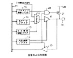
図2は、従来の入出力回路の一例を示す構成図である。
この入出力回路は、マイクロコンピュータの集積回路に組込まれるもので、内部バス11に接続された入出力制御レジスタ12、2次機能制御レジスタ13、出力データレジスタ14、及びプルアップ制御レジスタ15等の機能設定用レジスタを有している。
【0004】
入出力制御レジスタ12は、内部バス11を介して与えられる入力モードまたは出力モードの制御コマンドを保持して入出力動作の切替えを行うものである。出力データレジスタ14は、出力モード時に内部バス11を介して与えられる出力データを保持するものである。2次機能制御レジスタ13は、出力モード時に、出力データレジスタ14内のデータを出力するか、2次機能として与えられるアドレス信号等を出力するかの切替え用の制御情報を保持するものである。プルアップ制御レジスタ15は、入力モード時に入力端子をプルアップするか否かの制御情報を保持するものである。
【0005】
出力データレジスタ14の出力側は、セレクタ16の第1の入力側に接続され、このセレクタ16の第2の入力側には、例えばアドレス信号等の2次機能出力信号が与えられるようになっている。セレクタ16は、2次機能制御レジスタ13から与えられる制御情報に基づいて、第1または第2の入力側の信号を選択して出力するものである。セレクタ16の出力側は、出力バッファ17を介して外部回路接続用の入出力端子18に接続されている。出力バッファ17は、入出力制御レジスタ12から与えられる出力モード信号OUTがレベル“H”になったときに、セレクタ16の出力信号を増幅して入出力端子18に接続された外部回路を駆動するものである。出力モード信号OUTがレベル“L”のときは、出力バッファ17の出力側はハイインピーダンス状態となって入出力端子18から切離されるようになっている。
【0006】
入出力端子18には、入力バッファ19の入力側が接続されている。入力バッファ19は、入出力制御レジスタ12から与えられる入力モード信号INが“H”になったときに、入出力端子18に外部回路から与えられる入力信号を内部バス11に出力するものである。入力モード信号INが“L”のときは、入力バッファ19の出力側はハイインピーダンス状態となって内部バス11から切離されるようになっている。
【0007】
入出力制御レジスタ12から出力される入力モード信号INとプルアップ制御レジスタ15の出力信号は、2入力の否定的論理積ゲート(以下、「NAND」という)20の入力側に与えられるようになっている。NAND20の出力側は、PチャネルMOSトランジスタ(以下、「PMOS」という)21のゲートに接続されている。PMOS21のソースは電源電位VDDに接続され、ドレインが入出力端子18に接続されている。
【0008】
このような入出力回路では、内部バス11を介して入出力制御レジスタ12に、入力モードまたは出力モードを設定することによって、入力回路とするか出力回路とするかの選択をすることができる。
入力モードを設定したときには、更にプルアップ制御レジスタ15に制御信号を設定することにより、PMOS21が導通状態になり、入出力端子18をプルアップすることができる。そして、外部回路から入出力端子18に入力された入力信号は入力バッファ19を介して内部バス11へ与えられる。
【0009】
一方、出力モードを設定したときには、更に2次機能制御レジスタ13に制御信号を設定することにより、出力データレジスタ14に格納されたデータ、または2次機能出力信号のいずれかをセレクタ16で選択して出力することができる。セレクタ16で選択された出力信号は、出力バッファ17で電力増幅されて入出力端子18に出力され、この入出力端子18に接続された外部回路が駆動される。
【0010】
【発明が解決しようとする課題】
しかしながら、従来の入出力回路では、次のような課題があった。
図3は、スタティック・ランダムアクセス・メモリ(以下、「SRAM」という)のデータ書込み時の信号タイミングを示す信号波形図である。
【0011】
この図3に示すように、SRAMでは、まずアドレス信号を与え、所定のアドレスセンス時間が経過してSRAM内のデコーダ等の状態が確定した時点で、ストローブ信号を与える(“L”にする)必要がある。また、書込むべきデータ信号を与えた後、所定のデータセットアップ時間が経過した後に、ストローブ信号を“H”にしなければならない。更に、ストローブ信号が“H”になった後も、所定のアドレスホールド時間の間、アドレス信号を変化させてはならない。また、所定のデータホールド時間の間、データ信号を変化させてはならない。これらのタイミング条件が満たされないと、SRAMにデータを正常に書込むことができなくなる。
【0012】
図2の入出力回路の出力モード時には、入出力端子18に接続される外部回路および接続方法により、出力信号と入力側外部回路とでタイミングに不整合が発生した場合、その外部回路が使用できなくなることがある。例えばSRAMを外部回路として接続した場合、入出力端子18からの出力信号であるアドレス信号、データ信号、ストローブ信号との間に適切なタイミング条件が整わないと、アクセスが困難になるという課題があった。更に、入力バッファ19や出力バッファ17の能力が、入出力端子18に接続される外部回路の入出力条件に整合していない場合、入出力波形の劣化により、データ誤りやデータ速度の低下を引起こすという課題があった。
【0013】
本発明は、前記従来技術が持っていた課題を解決し、入出力信号のタイミング調整や、入出力条件の選択が可能な入出力回路を提供するものである。
【0014】
【課題を解決するための手段】
前記課題を解決するために、本発明のうちの請求項1に係る発明は、マイクロコントローラの集積回路に組込まれ、前記集積回路の入出力端子を介して接続される外部回路との間でデータまたは信号の入出力を行う入出力回路において、前記入出力端子に出力する前記データまたは前記信号を遅延させる遅延手段を備え、前記遅延手段は、直列に接続された複数の遅延素子を有し、前記複数の遅延素子のうちの任意のいくつかの前記遅延素子の出力を用いて複数の遅延時間分遅延させた複数の遅延信号を生成し、制御情報に基づいて、生成された前記複数の遅延信号のいずれか1つあるいは、前記複数の遅延信号の任意のいくつかを組合せた信号を出力信号として前記入出力端子へ出力するものであることを特徴とする。
【0015】
請求項2に係る発明は、請求項1記載の入出力回路において、更に、駆動能力の異なる複数の出力バッファを有し、前記出力バッファの中から予め選択された前記出力バッファを介して前記データまたは前記信号を前記入出力端子に出力する出力手段を備えたことを特徴とする。
【0016】
請求項3に係る発明は、請求項1または2記載の入出力回路において、更に、入力特性の異なる複数の入力バッファを有し、前記入出力端子に与えられた前記データまたは前記信号を前記入力バッファの中から予め選択された前記入力バッファを介して入力する入力手段を備えたことを特徴とする。
【0017】
請求項4に係る発明は、請求項3記載の入出力回路において、入力モード時に、前記入出力端子を所定の電位にするか否かを選択的に制御可能な構成にしたことを特徴とする。
【0018】
請求項5に係る発明は、請求項1〜4のいずれか1項に記載の入出力回路中の遅延手段において、前記制御情報は第1の情報と第2の情報とを有し、更に、前記第1の情報に基づき、前記複数の遅延信号のうちのいくつかを選択的に出力する選択出力段と、前記選択出力段から選択的に出力された信号に基づいて組合せた信号を生成し、前記第2の情報に基づき、前記複数の遅延信号のいずれか1つあるいは、前記複数の遅延信号の任意のいくつかを組合せた前記出力信号を出力する信号生成段とを有することを特徴とする。
【0019】
請求項6に係る発明は、請求項5記載の入出力回路において、前記信号生成段は、 選択的に出力された前記信号に基づいて組合せた前記信号を生成して出力する第1の信号生成回路と、前記第2の情報に基づいて、前記第1の信号生成回路の出力から、前記出力信号を生成して出力する第2の信号生成回路とを有することを特徴とする。
【0020】
【発明の実施の形態】
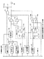
図1は、本発明の実施形態を示す入出力回路の構成図であり、図2中の要素と共通の要素には共通の符号が付されている。
この入出力回路は、マイクロコンピュータ等の集積回路に組込まれるものである。この入出力回路は、図2と同様の入出力制御レジスタ12、2次機能制御レジスタ13、出力データレジスタ14、及びプルアップ制御レジスタ15に加えて、出力切替レジスタ22及び入力切替レジスタ23の機能設定用レジスタを有している。これらのレジスタは、内部バス11に接続されている。
【0021】
入出力制御レジスタ12は、内部バス11を介して与えられる入力モードまたは出力モードを指定するための制御コマンドを保持し、入出力動作の切替えを行うものである。入出力制御レジスタ12に入力モードが設定されたときには、“H”の入力モード信号INが出力され、出力モードが設定されたときには、“H”の出力モード信号OUTが出力されるようになっている。
【0022】
出力データレジスタ14は、出力モード時に内部バス11を介して与えられる出力データを保持するものである。2次機能制御レジスタ13は、出力モード時に、出力データレジスタ14内のデータを出力するか、2次機能として与えられるアドレス信号等を出力するかの切替え用の制御情報を保持するものである。プルアップ制御レジスタ15は、入力モード時に入出力端子18をプルアップするか否かの制御情報を保持するものである。
【0023】
一方、出力切替レジスタ22は、出力バッファの駆動能力を切替えるための制御信号を保持するものである。例えば、駆動能力の高い出力バッファを選択するときには、出力切替レジスタ22に“H”の制御信号を保持し、駆動能力の低い出力バッファを選択するときには、“L”の制御信号を保持するようになっている。また、入力切替レジスタ23は、入力バッファの入力レベルを切替えるための制御信号を保持するものである。例えば、TTLレベルの入力バッファを選択するときには、入力切替レジスタに“H”の制御信号を保持し、CMOSレベルの入力バッファを選択するときには、“L”の制御信号を保持するようになっている。
【0024】
出力データレジスタ14の出力側は、セレクタ16の第1の入力側に接続され、このセレクタ16の第2の入力側には、例えばアドレス信号等の2次機能出力信号が与えられるようになっている。セレクタ16は、2次機能制御レジスタ13から与えられる制御情報に基づいて、第1または第2の入力側の信号を選択して出力するものである。セレクタ16の出力側は、遅延手段(例えば、遅延回路)30の入力側に接続されている。
【0025】
遅延回路30は、セレクタ16の出力信号を、内部バス11から与えられる制御信号に基づいて遅延させるものであり、この遅延回路30の出力側が、駆動能力の異なる出力バッファ17a,17bの入力側に接続されている。出力バッファ17a,17bの出力側は、外部回路接続用の入出力端子18に接続されている。出力バッファ17a,17bは、いずれも制御端子に与えられる制御信号が“H”の時に、遅延回路30の出力信号を増幅して入出力端子18に接続された外部回路を駆動するものである。また、出力バッファ17a,17bの制御端子に与えられる制御信号が“L”の時には、その出力側がハイインピーダンス状態となって入出力端子18から切離されるようになっている。なお、出力バッファ17aは、出力バッファ17bに比べて駆動能力が大きく設定されている。
【0026】
出力切替レジスタ22の出力側には、デコーダ24が接続されている。デコーダ24は、例えば2入力の論理積ゲート(以下、「AND」という)24a,24bとインバータ24cで構成されている。デコーダ24は、入出力制御レジスタ12から出力される出力モード信号OUTが“H”のとき、出力切替レジスタ22の出力信号の“H”,“L”に対応して、それぞれAND24a,24bから“H”の信号を出力するものである。AND24a,24bの出力側は、それぞれ出力バッファ17a,17bの制御端子に接続されている。
【0027】
入出力端子18には、入力バッファ19a,19bの入力側が接続されている。入力バッファ19a,19bは、制御端子に与えられる制御信号が“H”になったときに、入出力端子18に外部回路から与えられる入力信号を内部バス11に出力するものである。制御信号が“L”のときは、入力バッファ19a,19bの出力側はハイインピーダンス状態となって内部バス11から切離されるようになっている。入力バッファ19aは、TTLレベルのバッファであり、また入力バッファ19bはCMOSレベルのバッファである。
【0028】
入力切替レジスタ23の出力側には、デコーダ25が接続されている。デコーダ25は、例えば2入力のAND25a,25bとインバータ25cで構成されている。デコーダ25は、入出力制御レジスタ12から出力される入力モード信号INが“H”のとき、入力切替レジスタ23の出力信号の“H”,“L”に対応して、それぞれAND25a,25bから“H”の信号を出力するものである。AND25a,25bの出力側は、それぞれ入力バッファ19a,19bの制御端子に接続されている。
【0029】
入出力制御レジスタ12から出力される入力モード信号INとプルアップ制御レジスタ15の出力信号は、2入力のNAND20の入力側に与えられるようになっている。NAND20の出力側は、PMOS21のゲートに接続されている。PMOS21のソースは電源電位VDDに接続され、ドレインが入出力端子18に接続されている。これらの入出力制御レジスタ12、プルアップ制御レジスタ15、NAND20、及びPMOS21により、入力モード時に、入出力端子18を所定の電位(プルアップ)にするか否かを選択的に制御可能な構成になっている。
【0030】
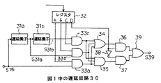
図4は、図1中の遅延回路30の一例を示す回路図である。
この遅延回路30は、セレクタ16の出力信号が与えられる遅延素子31aとこの後段に接続された遅延素子31b、及び内部バス11から制御信号が設定されるレジスタ32を有している。レジスタ32は、制御情報のうちの第1の情報を出力する出力端子A,B,Cと、制御情報のうちの第2の情報を出力する出力端子Dとを有している。遅延素子31aの入力側と出力側、及び遅延素子31aの出力側は、それぞれ2入力のAND33a,33b,33cからなる選択出力段の第1の入力側に接続されている。AND33a〜33cの第2の入力側は、それぞれレジスタ32の出力端子A,B,Cに接続されている。
【0031】
AND33a〜33cの出力側は、3入力の論理和ゲート(以下、「OR」という)34、及びAND35からなる第1の信号生成回路の入力側に接続されている。OR34及びAND35の出力側は、それぞれ2入力のAND36,37の第1の入力側に接続されている。AND36の第2の入力側はレジスタ32の出力端子Dに接続され、AND37の第2の入力側はインバータ38を介してレジスタ32の出力端子Dに接続されている。更に、AND36,37の出力側は2入力のOR39の入力側に接続され、このOR39の出力側が出力バッファ17a,17bの入力側に接続されている。AND36,37及びOR39により、第2の信号生成回路が構成され、この第2の信号生成回路と、前記第1の信号生成回路とにより、信号生成段が構成されている。
【0032】
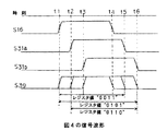
図5は、図4の遅延回路30の機能を説明するための信号波形図である。
図4において、入力された信号S16は、遅延素子31a,31bで遅延されて、それぞれ信号S31a,S31bとなる。これらの信号S16,S31a,S31bは、レジスタ32の出力端子A,B,C,Dから出力される4ビットの制御信号の内のビット0(A),1(B),2(C)に対応している。制御信号の対応するビットが論理値“1”に設定された信号が、AND33a〜33cで選択され、OR34及びAND35からそれぞれ信号S34,S35が出力される。信号S34,S35は、AND36,37、インバータ38及びOR39で構成されるセレクタに入力され、レジスタ32の出力端子Dから出力される制御信号に従って、いずれか一方が選択されて信号S39として出力される。
【0033】
図5に示すように、例えば時刻t1で信号S16が立上がると、この信号S16は遅延素子31aで遅延され、時刻t2で信号S31aが立上がる。更に信号S31aは遅延素子31bで遅延され、時刻t3で信号S31bが立上がる。
時刻t4で信号S16が立下がると、この信号S16は遅延素子31aで遅延され、時刻t5で信号S31aが立下がる。更に信号S31aは遅延素子31bで遅延され、時刻t6で信号S31bが立下がる。
【0034】
ここで、レジスタ32の設定値を“0001”とすれば、信号S16と同じタイミングの信号が信号S39として出力される。また、レジスタ32の設定値を“0010”とすれば、信号S31aと同じタイミングの信号が信号S39として出力され、更にレジスタ32の設定値を“0100”とすれば、信号S31bと同じタイミングの信号が信号S39として出力される。
【0035】
また、レジスタ32のビット0〜2の内の2ビットを“1”に設定することにより、信号S16及び信号S31a,31bを組合わせたタイミングの信号を信号S39として出力することができる。例えば、レジスタ32の設定値を“0011”とすれば、時刻t1〜t5の幅を有する信号S39が得られる。また、レジスタ32の設定値を“0101”とすれば、時刻t1〜t6の幅を有する信号S39が得られ、この設定値を“0110”とすれば、時刻t2〜t6の幅を有する信号S39が得られる。
【0036】
更に、レジスタ32のビット3を“1”に設定することにより、それぞれビット0〜2で指定した信号S16,S31a,S31b,S39の反転信号を得ることができる。
【0037】
次に、図1の動作を、(I)入力モードと、(II)出力モードに分けて説明する。
(I) 入力モード
内部バス11を介して入出力制御レジスタ12に、入力モードを設定すると、この入出力制御レジスタ12から出力される入力モード信号INが“H”となる。一方、入出力制御レジスタ12から出力される出力モード信号OUTは“L”となり、デコーダ24の出力信号は2つとも“L”となって出力バッファ17a,17bの出力側はハイインピーダンス状態となって入出力端子18から切離される。
【0038】
また、入出力端子18に接続される外部回路の出力条件がTTLレベルかCMOSレベルかに基づいて、入力切替レジスタ23に“1”または“0”を設定する。ここで、入力切替レジスタ23に“1”を設定すると、デコーダ25のAND25aの出力信号が“H”となり、入出力端子18はTTLレベルの入力バッファ19aを介して内部バス11に接続される。一方、入力切替レジスタ23に“0”を設定すると、デコーダ25のAND25bの出力信号が“H”となり、入出力端子18はCMOSレベルの入力バッファ19bを介して内部バス11に接続される。
【0039】
更に、入出力端子18をプルアップする場合、プルアップ制御レジスタ15に“1”を設定する。これにより、NAND20の出力信号が“L”となり、PMOS21がオン状態になって入出力端子18がプルアップされる。一方、プルアップ制御レジスタ15に“0”を設定すると、NAND20の出力信号は“H”となり、PMOS21はオフ状態となってプルアップは行われない。
【0040】
このように、入力切替レジスタ23によって入力レベルの設定を行って入力バッファ19a,19bのいずれかを選択し、プルアップ制御レジスタ15によってプルアップの要否を設定することにより、この入出力回路は、外部回路のインタフェース条件に合った入力回路に設定される。そして、入出力端子18に入力された入力信号は、入力バッファ19aまたは19bを介して内部バス11へ出力される。
【0041】
(II) 出力モード
内部バス11を介して入出力制御レジスタ12に、出力モードを設定すると、この入出力制御レジスタ12から出力される出力モード信号OUTが“H”となる。一方、入出力制御レジスタ12から出力される入力モード信号INは“L”となり、デコーダ25の出力信号は2つとも“L”となって入力バッファ19a,19bの出力側はハイインピーダンス状態となって内部バス11から切離される。更に、NAND20の出力信号は“H”となって、PMOS21はオフ状態となる。
【0042】
また、入出力端子18に接続される外部回路の負荷の大小に基づいて、出力切替レジスタ22に“1”または“0”を設定する。ここで、出力切替レジスタ22に“1”を設定すると、デコーダ24のAND24aの出力信号が“H”となり、遅延回路30の出力側は、駆動能力の大きな出力バッファ17aを介して入出力端子18に接続される。一方、出力切替レジスタ22に“0”を設定すると、デコーダ24のAND24bの出力信号が“H”となり、遅延回路30の出力側は、駆動能力の小さな出力バッファ17bを介して入出力端子18に接続される。
【0043】
更に、内部バス11から遅延回路30に対して遅延時間を設定すると共に、出力データレジスタ14に格納されたデータ及び2次機能出力信号のいずれを出力するかの制御信号を、2次機能制御レジスタ13に設定する。
これにより、セレクタ16で選択された出力信号が、遅延回路30で所定の時間だけ遅延され、出力バッファ17aまたは17bで所定の電力に増幅されて入出力端子18に出力され、この入出力端子18に接続された外部回路が駆動される。
【0044】
このように、本実施形態の入出力回路は、次の(1)〜(3)のような利点がある。
(1) 出力モード時に、アドレス信号等の2次機能出力信号や出力データの出力タイミングを任意の時間だけ遅延させたり、出力する信号の時間を増減することができる遅延回路30を有している。これにより、この入出力回路を外部バス機能として使用した場合に、2次機能として出力するアドレス信号、データ信号、及びストローブ信号等の出力タイミングを変更することが可能となり、入出力端子18に接続されるSRAM等の外部回路のタイミング条件に合わせることができる。また、クロック同期式シリアルポートの出力回路として使用する場合、送信用クロック信号及び送信データのタイミングを変更することが可能であるので、通信相手となる外部回路の周辺装置に合わせて、送信データセットアップ時間や送信データホールド時間を調整することができる。これにより、接続可能な外部回路の種類を増やすことができる。
【0045】
(2) 駆動能力の異なる出力バッファ17a,17bを有すると共に、これらの出力バッファ17a,17bを切替えるための出力切替レジスタ22及びデコーダ24を有している。これにより、外部回路の負荷容量の増大により、能力の小さな出力バッファ17bでは駆動能力が不足した場合に、駆動能力の大きな出力バッファ17aに切替えることにより、出力信号の鈍りによる遅延を解消することができる。また、2次機能である外部バス機能及び同期式シリアルポート使用時にも、駆動能力を変更することができるので、出力信号の立上がりを速くしたり、遅くしたりすることで、出力信号のセットアップ時間及びホールド時間を調整することが可能である。
【0046】
(3) 入力レベルの異なる入力バッファ19a,19bを有すると共に、これらの入力バッファ19a,19bを切替えるための入力切替レジスタ23及びデコーダ25を有している。これにより、外部回路の出力条件に合わせることができるので、接続可能な外部回路の種類を増やすことができる。また、外部バス機能及び同期式シリアルポート使用時にも、入力レベルを変更することができるので、入力信号の取り込みを速くしたり、遅くしたりすることで、入力信号のセットアップ時間及びホールド時間を調整することが可能である。
【0047】
なお、本発明は、上記実施形態に限定されず、種々の変形が可能である。この変形例としては、例えば、次の(a)〜(f)のようなものがある。
(a) 遅延回路30の構成は、図4に限定されない。即ち、遅延素子を3個以上に増加して設定できる遅延時間の数を増やすことができる。これにより、時間調整範囲が広がり接続可能な外部回路の種類を更に増やすことができる。また、遅延素子にカウンタを用いることによりクロックベースで遅延時間の調整が可能である。
【0048】
(b) 遅延回路30は、レジスタ32によって遅延時間の設定がプログラム可能になっているが、このレジスタ32に代えて遅延時間設定用のスイッチや外部端子を設けても良い。このような設定スイッチ等は、電源投入当初の初期設定以前に、正常な動作が必要な入出力回路の場合に有効である。
【0049】
(c) 選択可能な入力バッファや出力バッファの数は2つに限定されない。例えば、入力バッファの種類は、TTLやCMOS等のレベル変換を行うものに限定されず、ヒステリシス特性を有するシュミット回路等を使用することもできる。入力バッファや出力バッファの数や種類を多くすることにより、接続可能な外部回路の種類を更に増やすことができる。
【0050】
(d) プルアップ制御レジスタ15と出力切替レジスタ22は、同時に使用することはないので、共用することが可能である。或いは、入力切替レジスタ23と出力切替レジスタ22を共用しても良い。
【0051】
(e) 外部回路の出力レベルが、例えばCMOSに決まっているのであれば、2種類の入力バッファを設ける必要はない。その場合、入力切替レジスタ23及びデコーダ25は不要となる。
【0052】
(f) 外部回路に対する駆動能力を切替える必要がなければ、2種類の出力バッファを設ける必要はない。その場合、出力切替レジスタ22及びデコーダ24は不要となる。
【0053】
【発明の効果】
以上詳細に説明したように、第1の発明(請求項1、5、6に係る発明)によれば、入出力端子に出力するデータまたは信号を、遅延させる遅延手段を有している。この遅延手段では、複数の遅延信号を生成して、これら遅延信号のいくつかを組合せた信号を生成してこれを出力信号として入出力端子へ出力する構成になっているので、入出力端子に出力する信号を任意の時間だけ遅延させたり、出力する信号の時間を増減することができる。これにより、外部回路のタイミング条件に合わせることが可能になり、タイミング条件が異なる各種のメモリや周辺回路に適合させて、効率の良い入出力動作が可能になる。
【0054】
第2の発明(請求項2、5、6に係る発明)によれば、予め選択した駆動能力を有する出力バッファを介してデータまたは信号を出力する出力手段を有している。これにより、外部回路の負荷容量に見合った出力バッファを使用することが可能になり、効率の良い入出力動作が可能になる。
【0055】
第3の発明(請求項3〜6に係る発明)によれば、予め選択した入力特性を有する入力バッファを介してデータまたは信号を入力する入力手段を有している。これにより、外部回路の出力条件に合致した入力バッファを使用することが可能になり、各種の外部回路に対応することができる。
【図面の簡単な説明】
【図1】本発明の実施形態を示す入出力回路の構成図である。
【図2】従来の入出力回路の一例を示す構成図である。
【図3】SRAMのデータ書込み時の信号タイミングを示す信号波形図である。
【図4】図1中の遅延回路30の一例を示す回路図である。
【図5】図4の遅延回路30の機能を説明するための信号波形図である。
【符号の説明】
11 内部バス
12 入出力制御レジスタ
13 2次機能制御レジスタ
14 出力データレジスタ
15 プルアップ制御レジスタ
16 セレクタ
17a,17b 出力バッファ
18 入出力端子
19a,19b 入力バッファ
20 NAND
21 PMOS
22 出力切替レジスタ
23 入力切替レジスタ
24,25 デコーダ[0001]
[Technical field to which the invention pertains]
The present invention relates to an input/output circuit for connecting an external circuit in an integrated circuit of a microcontroller.
[0002]
2. Description of the Related Art
In general, input/output circuits used in microcontrollers such as microcomputers are designed to allow one external connection interface to be switched between being used as an input or output circuit for digital signals by rewriting a function setting register with a program. Furthermore, some input/output circuits can be used as an output circuit for address signals and data signals for an external bus, or as an input circuit with a pull-up as a secondary function.
[0003]
FIG. 2 is a configuration diagram showing an example of a conventional input/output circuit.
This input/output circuit is incorporated into an integrated circuit of a microcomputer and has function setting registers such as an input/
[0004]
The input/
[0005]
The output side of the
[0006]
The input side of an
[0007]
The input mode signal IN output from the input/
[0008]
In such an input/output circuit, by setting the input mode or output mode in the input/
When the input mode is set, a control signal can be further set in the pull-up
[0009]
On the other hand, when the output mode is set, a control signal is further set in the secondary
[0010]
[Problem to be solved by the invention]
However, the conventional input/output circuits have the following problems.
FIG. 3 is a signal waveform diagram showing signal timing when writing data to a static random access memory (hereinafter referred to as "SRAM").
[0011]
As shown in Fig. 3, in an SRAM, an address signal must first be applied, and once a certain address sense time has elapsed and the state of the decoder and other components within the SRAM has been established, a strobe signal must be applied (set to "L"). After the data signal to be written is applied, the strobe signal must be set to "H" after a certain data setup time has elapsed. Furthermore, even after the strobe signal has become "H", the address signal must not be changed for a certain address hold time. Furthermore, the data signal must not be changed for a certain data hold time. If these timing conditions are not met, data cannot be written correctly to the SRAM.
[0012]
2, if a timing mismatch occurs between the output signal and the input side external circuit due to the external circuit and the connection method connected to the input/
[0013]
The present invention solves the problems associated with the conventional techniques and provides an input/output circuit that allows adjustment of input/output signal timing and selection of input/output conditions.
[0014]
[Means for solving the problem]
In order to solve the above problem, the invention according to
[0015]
The invention according to claim 2 is characterized in that the input/output circuit according to
[0016]
The invention according to claim 3 is characterized in that, in the input/output circuit according to
[0017]
According to a fourth aspect of the present invention, in the input/output circuit of the third aspect, the input/output terminal is selectively controlled to be set to a predetermined potential or not in an input mode.
[0018]
The invention of claim 5 is characterized in that, in the delay means in the input/output circuit described in any one of
[0019]
The invention according to claim 6 is characterized in that in the input/output circuit according to claim 5, the signal generation stage has a first signal generation circuit that generates and outputs the combined signal based on the selectively output signals, and a second signal generation circuit that generates and outputs the output signal from the output of the first signal generation circuit based on the second information.
[0020]
[0023]
FIG. 1 is a block diagram of an input/output circuit showing an embodiment of the present invention, and elements common to those in FIG. 2 are given the same reference numerals.
This input/output circuit is incorporated in an integrated circuit such as a microcomputer. This input/output circuit has function setting registers, an
[0021]
The input/output control register 12 holds a control command for specifying an input mode or an output mode given via the
[0022]
The output data register 14 holds output data provided via the
[0023]
On the other hand, the
[0024]
The output side of the output data register 14 is connected to a first input side of a
[0025]
The
[0026]
A decoder 24 is connected to the output side of the
[0027]
The input sides of
[0028]
A
[0029]
The input mode signal IN output from the input/
[0030]
FIG. 4 is a circuit diagram showing an example of the
The
[0031]
The output sides of the ANDs 33a to 33c are connected to the input sides of a first signal generating circuit consisting of a three-input logical OR gate (hereinafter referred to as "OR") 34 and an AND 35. The output sides of the
[0032]
FIG. 5 is a signal waveform diagram for explaining the function of the
In Fig. 4, the input signal S16 is delayed by
[0033]
5, when the signal S16 rises at time t1, the signal S16 is delayed by the
When the signal S16 falls at time t4, the signal S16 is delayed by the
[0034]
Here, if the set value of
[0035]
Furthermore, by setting two bits out of bits 0 to 2 of
[0036]
Furthermore, by setting bit 3 of
[0037]
Next, the operation of FIG. 1 will be explained separately for (I) an input mode and (II) an output mode.
(I) Input Mode When an input mode is set in the input/output control register 12 via the
[0038]
Also, based on whether the output condition of the external circuit connected to the input/
[0039]
Furthermore, when the input/
[0040]
In this way, the input level is set by the
[0041]
(II) Output Mode When an output mode is set in the input/output control register 12 via the
[0042]
Also, the
[0043]
Furthermore, a delay time is set in the
As a result, the output signal selected by the
[0044]
As described above, the input/output circuit of this embodiment has the following advantages (1) to (3).
(1) In the output mode, the
[0045]
(2) The device has
[0046]
(3) It has
[0047]
The present invention is not limited to the above-described embodiment, and various modifications are possible. Examples of such modifications include the following (a) to (f).
(a) The configuration of the
[0048]
(b) In the
[0049]
(c) The number of selectable input buffers and output buffers is not limited to two. For example, the type of input buffer is not limited to those that perform level conversion such as TTL and CMOS, and a Schmitt circuit having a hysteresis characteristic can also be used. By increasing the number and types of input buffers and output buffers, the types of connectable external circuits can be further increased.
[0050]
(d) The pull-up
[0051]
(e) If the output level of the external circuit is determined to be, for example, CMOS, there is no need to provide two types of input buffers. In that case, the
[0052]
(f) If there is no need to switch the drive capability for an external circuit, there is no need to provide two types of output buffers. In that case, the
[0053]
Effect of the Invention
As described above in detail, the first invention (invention according to
[0054]
According to the second aspect of the present invention (invention related to claims 2, 5 and 6) , there is provided an output means for outputting data or a signal via an output buffer having a preselected driving capability, which makes it possible to use an output buffer suited to the load capacitance of an external circuit, thereby enabling efficient input/output operations.
[0055]
According to the third aspect of the invention (inventions related to claims 3 to 6) , there is provided an input means for inputting data or signals via an input buffer having preselected input characteristics, which makes it possible to use an input buffer that matches the output conditions of an external circuit, and thus makes it possible to support various external circuits.
[Brief description of the drawings]
FIG. 1 is a configuration diagram of an input/output circuit showing an embodiment of the present invention.
FIG. 2 is a configuration diagram showing an example of a conventional input/output circuit.
FIG. 3 is a signal waveform diagram showing signal timing when data is written to an SRAM.
4 is a circuit diagram showing an example of a
5 is a signal waveform diagram for explaining the function of the
[Explanation of symbols]
11
21 PMOS
22
Claims (6)
前記入出力端子に出力する前記データまたは前記信号を遅延させる遅延手段を備え、
前記遅延手段は、直列に接続された複数の遅延素子を有し、前記複数の遅延素子のうちの任意のいくつかの前記遅延素子の出力を用いて複数の遅延時間分遅延させた複数の遅延信号を生成し、制御情報に基づいて、生成された前記複数の遅延信号のいずれか1つあるいは、前記複数の遅延信号の任意のいくつかを組合せた信号を出力信号として前記入出力端子へ出力するものであることを特徴とする入出力回路。 An input/output circuit that is incorporated in an integrated circuit of a microcontroller and inputs/outputs data or signals between an external circuit connected via an input/output terminal of the integrated circuit,
a delay means for delaying the data or the signal to be output to the input/output terminal;
The delay means has a plurality of delay elements connected in series, generates a plurality of delayed signals delayed by a plurality of delay times using the outputs of any of the plurality of delay elements, and outputs any one of the generated delayed signals or a signal combining any of the plurality of delayed signals as an output signal to the input/output terminal based on control information.
駆動能力の異なる複数の出力バッファを有し、前記出力バッファの中から予め選択された前記出力バッファを介して前記データまたは前記信号を前記入出力端子に出力する出力手段を備えたことを特徴とする入出力回路。 The input/output circuit according to claim 1 further comprises:
1. An input/output circuit comprising: a plurality of output buffers each having a different driving capability; and output means for outputting the data or the signal to the input/ output terminal via an output buffer previously selected from among the output buffers.
入力特性の異なる複数の入力バッファを有し、前記入出力端子に与えられた前記データまたは前記信号を前記入力バッファの中から予め選択された前記入力バッファを介して入力する入力手段を備えたことを特徴とする入出力回路。 The input/output circuit according to claim 1 or 2 further comprises:
1. An input/output circuit comprising: a plurality of input buffers each having a different input characteristic; and input means for inputting the data or the signal applied to the input/ output terminal through an input buffer previously selected from among the input buffers.
前記制御情報は第1の情報と第2の情報とを有し、更に、The control information includes first information and second information, and further includes:
前記第1の情報に基づき、前記複数の遅延信号のうちのいくつかを選択的に出力する選択出力段と、a selection output stage that selectively outputs some of the plurality of delayed signals based on the first information;
前記選択出力段から選択的に出力された信号に基づいて組合せた信号を生成し、前記第2の情報に基づき、前記複数の遅延信号のいずれか1つあるいは、前記複数の遅延信号の任意のいくつかを組合せた前記出力信号を出力する信号生成段と、a signal generating stage that generates a combined signal based on the signal selectively output from the selection output stage, and outputs the output signal that is a combination of any one of the plurality of delayed signals or any of some of the plurality of delayed signals based on the second information;
を有することを特徴とする請求項1〜4のいずれか1項に記載の入出力回路。5. The input/output circuit according to claim 1, further comprising:
選択的に出力された前記信号に基づいて組合せた前記信号を生成して出力する第1の信号生成回路と、a first signal generating circuit that generates and outputs the combined signal based on the selectively outputted signals;
前記第2の情報に基づいて、前記第1の信号生成回路の出力から、前記出力信号を生成して出力する第2の信号生成回路と、a second signal generating circuit that generates the output signal from an output of the first signal generating circuit based on the second information and outputs the output signal;
を有することを特徴とする請求項5記載の入出力回路。6. The input/output circuit according to claim 5, further comprising:
Priority Applications (1)
| Application Number | Priority Date | Filing Date | Title |
|---|---|---|---|
| JP2000206692A JP4384792B2 (en) | 2000-07-07 | 2000-07-07 | Input/Output Circuit |
Applications Claiming Priority (1)
| Application Number | Priority Date | Filing Date | Title |
|---|---|---|---|
| JP2000206692A JP4384792B2 (en) | 2000-07-07 | 2000-07-07 | Input/Output Circuit |
Publications (2)
| Publication Number | Publication Date |
|---|---|
| JP2002026713A JP2002026713A (en) | 2002-01-25 |
| JP4384792B2 true JP4384792B2 (en) | 2009-12-16 |
Family
ID=18703576
Family Applications (1)
| Application Number | Title | Priority Date | Filing Date |
|---|---|---|---|
| JP2000206692A Expired - Lifetime JP4384792B2 (en) | 2000-07-07 | 2000-07-07 | Input/Output Circuit |
Country Status (1)
| Country | Link |
|---|---|
| JP (1) | JP4384792B2 (en) |
Families Citing this family (2)
| Publication number | Priority date | Publication date | Assignee | Title |
|---|---|---|---|---|
| DE102005005090B3 (en) * | 2005-02-03 | 2006-07-13 | Infineon Technologies Ag | Method for switching between parallel-circuited electronic modules, requires storage of configuration value in first programmable register |
| JP5695538B2 (en) * | 2011-10-07 | 2015-04-08 | ルネサスエレクトロニクス株式会社 | Semiconductor device |
-
2000
- 2000-07-07 JP JP2000206692A patent/JP4384792B2/en not_active Expired - Lifetime
Also Published As
| Publication number | Publication date |
|---|---|
| JP2002026713A (en) | 2002-01-25 |
Similar Documents
| Publication | Publication Date | Title |
|---|---|---|
| US5319258A (en) | Programmable output drive circuit | |
| KR980011424A (en) | Digital signal transmission device | |
| JP3820559B2 (en) | Mode register set circuit of semiconductor device | |
| KR100223675B1 (en) | Data-output-related circuit suitable for high speed semiconductor memory device | |
| US6249461B1 (en) | Flash memory device with a status read operation | |
| JP2003044349A (en) | Register and signal generation method | |
| JP3394111B2 (en) | Data input circuit of semiconductor memory device | |
| JP4384792B2 (en) | Input/Output Circuit | |
| USRE41441E1 (en) | Output buffer having inherently precise data masking | |
| JP2805466B2 (en) | Memory address transition detection circuit | |
| JPH09238068A (en) | Output driver circuit with single through-rate resistor | |
| US6195296B1 (en) | Semiconductor memory device and system | |
| JP7251624B2 (en) | semiconductor integrated circuit | |
| JP3630847B2 (en) | Latch circuit | |
| JP2006203568A (en) | Slew rate control device, output buffer, and information processing device | |
| JP2011135436A (en) | Semiconductor device | |
| KR960011208B1 (en) | Semiconductor memory device | |
| US7978547B2 (en) | Data I/O control signal generating circuit in a semiconductor memory apparatus | |
| US5905678A (en) | Control circuit of an output buffer | |
| JP3057710B2 (en) | Semiconductor memory device | |
| US7649789B2 (en) | Semiconductor memory device with various delay values | |
| JP2682394B2 (en) | Multiplexer circuit | |
| JP3723993B2 (en) | Low-speed guaranteed read-only memory | |
| US5513141A (en) | Single port register | |
| US20070052466A1 (en) | Flip-flop with improved operating speed |
Legal Events
| Date | Code | Title | Description |
|---|---|---|---|
| A621 | Written request for application examination |
Free format text: JAPANESE INTERMEDIATE CODE: A621 Effective date: 20061027 |
|
| A977 | Report on retrieval |
Free format text: JAPANESE INTERMEDIATE CODE: A971007 Effective date: 20080827 |
|
| A131 | Notification of reasons for refusal |
Free format text: JAPANESE INTERMEDIATE CODE: A131 Effective date: 20080902 |
|
| A521 | Written amendment |
Free format text: JAPANESE INTERMEDIATE CODE: A523 Effective date: 20081104 |
|
| A711 | Notification of change in applicant |
Free format text: JAPANESE INTERMEDIATE CODE: A712 Effective date: 20081218 |
|
| RD02 | Notification of acceptance of power of attorney |
Free format text: JAPANESE INTERMEDIATE CODE: A7422 Effective date: 20090422 |
|
| TRDD | Decision of grant or rejection written | ||
| A01 | Written decision to grant a patent or to grant a registration (utility model) |
Free format text: JAPANESE INTERMEDIATE CODE: A01 Effective date: 20090901 |
|
| A01 | Written decision to grant a patent or to grant a registration (utility model) |
Free format text: JAPANESE INTERMEDIATE CODE: A01 |
|
| A61 | First payment of annual fees (during grant procedure) |
Free format text: JAPANESE INTERMEDIATE CODE: A61 Effective date: 20090928 |
|
| FPAY | Renewal fee payment (event date is renewal date of database) |
Free format text: PAYMENT UNTIL: 20121002 Year of fee payment: 3 |
|
| R150 | Certificate of patent or registration of utility model |
Free format text: JAPANESE INTERMEDIATE CODE: R150 |