JP4384183B2 - Magnetoresistive element and magnetic memory - Google Patents
Magnetoresistive element and magnetic memory Download PDFInfo
- Publication number
- JP4384183B2 JP4384183B2 JP2007016930A JP2007016930A JP4384183B2 JP 4384183 B2 JP4384183 B2 JP 4384183B2 JP 2007016930 A JP2007016930 A JP 2007016930A JP 2007016930 A JP2007016930 A JP 2007016930A JP 4384183 B2 JP4384183 B2 JP 4384183B2
- Authority
- JP
- Japan
- Prior art keywords
- layer
- magnetization
- magnetoresistive element
- tunnel barrier
- magnetization free
- Prior art date
- Legal status (The legal status is an assumption and is not a legal conclusion. Google has not performed a legal analysis and makes no representation as to the accuracy of the status listed.)
- Active
Links
Images


Classifications
-
- H—ELECTRICITY
- H10—SEMICONDUCTOR DEVICES; ELECTRIC SOLID-STATE DEVICES NOT OTHERWISE PROVIDED FOR
- H10B—ELECTRONIC MEMORY DEVICES
- H10B61/00—Magnetic memory devices, e.g. magnetoresistive RAM [MRAM] devices
- H10B61/20—Magnetic memory devices, e.g. magnetoresistive RAM [MRAM] devices comprising components having three or more electrodes, e.g. transistors
- H10B61/22—Magnetic memory devices, e.g. magnetoresistive RAM [MRAM] devices comprising components having three or more electrodes, e.g. transistors of the field-effect transistor [FET] type
-
- G—PHYSICS
- G11—INFORMATION STORAGE
- G11C—STATIC STORES
- G11C11/00—Digital stores characterised by the use of particular electric or magnetic storage elements; Storage elements therefor
- G11C11/02—Digital stores characterised by the use of particular electric or magnetic storage elements; Storage elements therefor using magnetic elements
- G11C11/14—Digital stores characterised by the use of particular electric or magnetic storage elements; Storage elements therefor using magnetic elements using thin-film elements
- G11C11/15—Digital stores characterised by the use of particular electric or magnetic storage elements; Storage elements therefor using magnetic elements using thin-film elements using multiple magnetic layers
-
- H—ELECTRICITY
- H10—SEMICONDUCTOR DEVICES; ELECTRIC SOLID-STATE DEVICES NOT OTHERWISE PROVIDED FOR
- H10N—ELECTRIC SOLID-STATE DEVICES NOT OTHERWISE PROVIDED FOR
- H10N50/00—Galvanomagnetic devices
- H10N50/10—Magnetoresistive devices
-
- H—ELECTRICITY
- H10—SEMICONDUCTOR DEVICES; ELECTRIC SOLID-STATE DEVICES NOT OTHERWISE PROVIDED FOR
- H10N—ELECTRIC SOLID-STATE DEVICES NOT OTHERWISE PROVIDED FOR
- H10N70/00—Solid-state devices without a potential-jump barrier or surface barrier, and specially adapted for rectifying, amplifying, oscillating or switching
- H10N70/801—Constructional details of multistable switching devices
Description
本発明は、磁気抵抗素子および磁気メモリに関する。 The present invention relates to a magnetoresistive element and a magnetic memory.
近年、新しい原理に基づいて情報を記録する固体メモリが多数提案されているが、中でも、固体磁気メモリとして、トンネル磁気抵抗(TMR(Tunneling Magnetoresistive))効果を利用する磁気ランダムアクセスメモリ(MRAM(Magnetoresistive Random Access Memory))が脚光を浴びている。MRAMは、データをMTJ((Magnetic Tunnel Junction))素子の磁化状態により記憶する点に特徴を有する。 In recent years, many solid-state memories that record information based on a new principle have been proposed. Among them, as a solid-state magnetic memory, a magnetic random access memory (MRAM (Magnetoresistive) that uses a tunneling magnetoresistive (TMR) effect is used. Random Access Memory)) is in the spotlight. The MRAM is characterized in that data is stored according to the magnetization state of an MTJ ((Magnetic Tunnel Junction)) element.
MTJ素子の近傍領域に配線を設けこの配線に流れる電流による磁界でMTJ素子の記憶層の磁化の向きを反転させることにより書き込みを行うMRAMにおいては、MTJ素子のサイズを縮小すると原理的にMTJ素子の保持力Hcが大きくなるために、MTJ素子のサイズ縮小にしたがって、配線に流れる電流によって誘起される磁界の強度を大きくする工夫が必要となり、高密度なメモリを作製することは困難である。 In an MRAM in which writing is performed by reversing the magnetization direction of the storage layer of the MTJ element by a magnetic field generated by a current flowing through the wiring provided in the vicinity of the MTJ element, the MTJ element is theoretically reduced when the size of the MTJ element is reduced. Since the holding force Hc increases, it is necessary to devise a technique for increasing the strength of the magnetic field induced by the current flowing in the wiring as the size of the MTJ element is reduced, and it is difficult to manufacture a high-density memory.
このような課題を克服する書き込み方式としてスピン角運動量移動(SMT(Spin Momentum Transfer))によりMTJ素子の記憶層の磁化の向きを反転させる書き込み方式を用いたMRAMが提案されている(例えば、特許文献1、非特許文献1〜2)。
As a writing method for overcoming such a problem, an MRAM using a writing method that reverses the magnetization direction of the storage layer of the MTJ element by spin angular momentum transfer (SMT) has been proposed (for example, patents).
スピン角運動量移動(以下、スピン注入と称する)による磁化反転では、磁化反転に必要な電流Icは、MTJ素子の持つ磁気異方性エネルギー(KuV)によって規定される。したがって、MTJ素子の面積が小さくなれば、スピン注入により磁化反転するための注入電流Icも小さくなる。先に述べた、電流によって誘導される磁界による書き込み方式に比べると、原理的にMTJ素子のサイズが小さくなれば書き込み電流も小さくなるために、スケーラビリティ性に優れることが期待される。
しかしながら、現状のMTJ素子のスピン注入の効率は現状では決して高くなく、磁化反転に必要な電流Icをより低減することが望まれている。 However, the efficiency of spin injection of the current MTJ element is never high at present, and it is desired to further reduce the current Ic necessary for magnetization reversal.
また高密度なメモリ応用を考える際、単純な構造を有しかつ単純なプロセスで上記電流の低減が行えることが切望されている。 Further, when considering high-density memory applications, it is desired that the current can be reduced with a simple structure and a simple process.
本発明は、上記事情を考慮してなされたものであって、磁化反転の際の反転電流をより低減することが可能な磁気抵抗素子およびそれを用いた磁気メモリを提供することを目的とする。 The present invention has been made in view of the above circumstances, and an object thereof is to provide a magnetoresistive element capable of further reducing a reversal current at the time of magnetization reversal and a magnetic memory using the same. .
本発明の第1の態様による磁気抵抗素子は、第1面およびこの第1面と反対側の第2面を有し磁化の向きが可変の磁化自由層と、前記磁化自由層の第1面および第2面のうち第1面側に設けられ磁化の向きが固着された磁化固着層と、前記磁化自由層と前記磁化固着層との間に設けられた第1トンネルバリア層と、前記磁化自由層の第2面に設けられた第2トンネルバリア層と、前記第2トンネルバリア層の前記磁化自由層と反対側の面に接するように設けられた非磁性層とを備え、前記磁化自由層の磁化の向きは、前記磁化固着層と前記非磁性層との間で通電することにより変化可能であり、前記第1トンネルバリア層と前記第2トンネルバリア層の抵抗比が1:0.25〜1:4の範囲にあることを特徴とする。 A magnetoresistive element according to a first aspect of the present invention includes a magnetization free layer having a first surface and a second surface opposite to the first surface and having a variable magnetization direction, and a first surface of the magnetization free layer. A magnetization pinned layer provided on the first surface side of the second surface and having a magnetization direction fixed; a first tunnel barrier layer provided between the magnetization free layer and the magnetization pinned layer; and the magnetization A second tunnel barrier layer provided on the second surface of the free layer; and a nonmagnetic layer provided on the surface of the second tunnel barrier layer opposite to the magnetization free layer, the magnetization free The magnetization direction of the layer can be changed by passing a current between the magnetization pinned layer and the nonmagnetic layer, and the resistance ratio of the first tunnel barrier layer to the second tunnel barrier layer is 1: 0. It is in the range of 25 to 1: 4.
また、本発明の第2の態様による磁気抵抗素子は、第1面およびこの第1面と反対側の第2面を有し磁化の向きが可変の磁化自由層と、前記磁化自由層の第1面および第2面のうち第1面側に設けられ磁化の向きが固着された磁化固着層と、前記磁化自由層と前記磁化固着層との間に設けられた第1トンネルバリア層と、前記磁化自由層の第2面に設けられた第2トンネルバリア層と、前記第2トンネルバリア層の前記磁化自由層と反対側の面に接するように設けられた非磁性層とを備え、前記磁化自由層の磁化の向きは、前記磁化固着層と前記非磁性層との間に通電することにより変化可能であり、前記第1トンネルバリア層と前記第2トンネルバリア層が同じ材料で形成されかつトンネル接合の面積が実質的に等しいとき、前記第2トンネルバリア層と前記第1トンネルバリア層の膜厚の差は0.14nm以下であることを特徴とする。 According to a second aspect of the present invention, there is provided a magnetoresistive element having a first surface and a second surface opposite to the first surface, the magnetization free layer having a variable magnetization direction, and the first layer of the magnetization free layer. A magnetization pinned layer provided on the first surface side of the first surface and the second surface and having a magnetization direction fixed; a first tunnel barrier layer provided between the magnetization free layer and the magnetization pinned layer; A second tunnel barrier layer provided on the second surface of the magnetization free layer, and a nonmagnetic layer provided so as to contact the surface of the second tunnel barrier layer opposite to the magnetization free layer, The magnetization direction of the magnetization free layer can be changed by passing a current between the magnetization pinned layer and the nonmagnetic layer, and the first tunnel barrier layer and the second tunnel barrier layer are formed of the same material. And when the area of the tunnel junction is substantially equal, The difference of the film thickness of Rubaria layer and the first tunnel barrier layer is equal to or less than 0.14 nm.
また、本発明の第3の態様による磁気メモリは、上記のいずれかに記載の磁気抵抗素子と、前記磁気抵抗素子の一端に接続される第1配線と、前記磁気抵抗素子の他端と電気的に接続される第2配線と、を備えたことを特徴とする。 According to a third aspect of the present invention, there is provided a magnetic memory according to any one of the above, the first wiring connected to one end of the magnetoresistive element, the other end of the magnetoresistive element, And a second wiring to be connected to each other.
本発明によれば、磁化反転の際の反転電流をより低減することが可能な磁気抵抗素子及びそれを用いた磁気メモリを提供することができる。 ADVANTAGE OF THE INVENTION According to this invention, the magnetoresistive element which can reduce the reversal current at the time of magnetization reversal, and a magnetic memory using the same can be provided.
(第1実施形態)
本発明の第1実施形態による磁気抵抗素子を説明する前に、第1実施形態の磁気抵抗素子を発明するに至った経緯を説明する。
(First embodiment)
Before explaining the magnetoresistive element according to the first embodiment of the present invention, the background of inventing the magnetoresistive element of the first embodiment will be explained.
まず、本発明者達は、第1の参考例として、図2示す第1の磁気抵抗素子50を作成した。この磁気抵抗素子50は、下部電極2と、この下部電極2上に形成された膜厚が20nmのPtMnからなる反強磁性層4と、この反強磁性層4上に形成され膜厚が2nmCoFe層、膜厚が0.6nmのRu層、および膜厚が2nmのCoFe層の積層構造を有する磁化固着層6と、この磁化固着層6上に形成された膜厚が1nmのMgOからなるトンネルバリア層8と、このトンネルバリア層8上に形成され膜厚が2nmのCoFeからなる磁化自由層(記憶層)10と、この磁化自由層10上に形成された膜厚が5nmのTaからなるキャップ層(図示せず)と、このキャップ層上に形成された上部電極14と、を備えている。なお、反強磁性層4は磁化固着層6の磁化の向きを固着する。図2に示す第1の磁気抵抗素子は、通常、下から上に電流を流した場合、すなわち電子を磁化自由層から磁化固着層へ流した場合の反転電流が大きい。
First, the inventors created a first
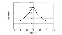
作成した磁気抵抗素子50の磁化固着層6の磁化向きと磁化自由層10の磁化の向きが逆向き、すなわち反平行(AP(Anti-Parallel))状態である場合の、抵抗変化率MRの印加電圧依存性を図3に示し、抵抗Rの印加電圧依存性を図4に示す。なお、印加電圧は上部電極14から下部電極2に電流を流すときを正にとり、下部電極2から上部電極14に電流を流すときを負にとってある。図3からわかるように、抵抗変化率MRは印加電圧の絶対値が0Vの状態から大きくなるにしたがって大きく低下する。これは、図4に示すようにAP状態の抵抗が0Vから電圧印加によって低下することによって起こる。
Application of the resistance change rate MR when the magnetization direction of the magnetization fixed
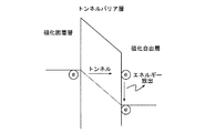
本発明者達が詳しく調査したところ、AP状態において電圧を印加することによる抵抗値の低下は、図5に示すように例えばピン層からの電子がトンネルバリア層を通過した後、透過先のフリー層のなかでエネルギーを放出するため、そのエネルギーによりフリー層が擾乱を受け、磁化方向が乱され、抵抗値が低下することに起因するとわかった。このときの電流Iを2回微分した値(d2I/dV2)を縦軸にとり、電圧Vを横軸にとったグラフを図6に示す。図6において実線で示すグラフは、Simmonsの式から導き出したものである。このSimmonsの式は、トンネルバリア層を2つの金属電極で挟んだ素子のI−V特性から導かれる。このSimmonsの式から導かれる特性と比較することより、図2に示す磁気抵抗素子50は、おおよそ0.08Vのあたりに極大点を持つことがわかる。これは、0Vから電圧が大きくなるにつれ、0.08Vまでは擾乱が大きくなることを示す。これより0.1V以上の電圧を印加することでトンネルした電子は磁性体の磁化を擾乱させることがわかる。なお、素子に印加される電圧は磁性層が金属なので、ほとんどトンネルバリア層に印加されることになる。
As a result of detailed investigations by the present inventors, the decrease in the resistance value due to the application of voltage in the AP state is, for example, that after electrons from the pinned layer pass through the tunnel barrier layer, the transmission destination is free as shown in FIG. It was found that because the energy is released in the layer, the free layer is disturbed by the energy, the magnetization direction is disturbed, and the resistance value decreases. FIG. 6 shows a graph in which the vertical axis represents the value (d 2 I / dV 2 ) obtained by differentiating the current I twice, and the horizontal axis represents the voltage V. The graph shown by the solid line in FIG. 6 is derived from the Simons equation. This Simons equation is derived from the IV characteristics of an element in which a tunnel barrier layer is sandwiched between two metal electrodes. By comparing with the characteristic derived from this Simons equation, it can be seen that the
次に、第2の参考例として、図2に示す第1の磁気抵抗素子において、トンネルバリア層の膜厚を1.0nmから0.6nmに変えた第2の磁気抵抗素子を作成した。そしてこの第2の磁気抵抗素子を、おおよそ100nm×150nmのサイズに加工した。この第2の磁気抵抗素子に電流を通電しながら、磁化自由層の磁化方向に平行な外部磁界を変化させ、磁化自由層の保持力Hcを測定し評価した結果を図7に示す。 Next, as a second reference example, a second magnetoresistive element in which the thickness of the tunnel barrier layer was changed from 1.0 nm to 0.6 nm in the first magnetoresistive element shown in FIG. The second magnetoresistive element was processed to a size of approximately 100 nm × 150 nm. FIG. 7 shows the result of measuring and evaluating the coercive force Hc of the magnetization free layer while changing the external magnetic field parallel to the magnetization direction of the magnetization free layer while passing a current through the second magnetoresistive element.
図7中の電流の向きは、磁化固着層から磁化自由層へ電流を流す向きを正としてある。なお、グラフg1は、電子を磁化固着層から磁化自由層へ注入した際の、磁化自由層の磁化の向きが磁化固着層に対して平行→反平行に変化するときのスイッチング磁界をプロットしたものであり、グラフg2は、磁化自由層の磁化の向きが反平行→平行に変化するときのスイッチング磁界をプロットしたものである。また、グラフg3は、磁化自由層から磁化固着層へ電子を注入した場合の、磁化自由層の磁化の向きが平行→反平行に変化するときのスイッチング磁界をプロットしたものであり、グラフg4は、磁化自由層の磁化の向きが反平行→平行に変化するときのスイッチング磁界をプロットしたものである。 The direction of current in FIG. 7 is positive when the current flows from the magnetization fixed layer to the magnetization free layer. The graph g 1 is when injected into magnetization free layer electrons from the magnetization pinned layer, the magnetization direction of the magnetization free layer is plotted switching magnetic field when varying parallel → anti-parallel to the magnetization pinned layer is intended, the graph g 2 are those in which a magnetization direction of the magnetization free layer is plotted switching magnetic field when varying antiparallel → parallel. A graph g 3 is a plot of the switching magnetic field when in the case of injecting electrons into the magnetization pinned layer from the magnetization free layer, the magnetization direction of the magnetization free layer changes in parallel → anti-parallel, the graph g 4 plots the switching magnetic field when the magnetization direction of the magnetization free layer changes from antiparallel to parallel.
図7からわかるように、磁化自由層にトンネルバリア層を介して電子を注入した場合における、磁化自由層の保持力Hc(同じ電流値に対する、グラフg1に示すスイッチング磁界と、グラフg2に示すスイッチング磁界との差)は、電流の大きさ(電流の絶対値)が大きくなるにつれて約67Oe/mAの割合で減少している。一方、上部電極からドリフトで電子を磁化自由層に注入した場合における、磁化自由層の保持力Hc(同じ電流値に対する、グラフg3に示すスイッチング磁界と、グラフg4に示すスイッチング磁界との差)は、電流の大きさ(電流の絶対値)が大きくなるにつれて28Oe/mAの割合で減少している。これらの現象を十分検討したところ、トンネルバリア層を介して電子が注入された場合、トンネルバリアに印加している電圧が、室温のエネルギー(おおよそ0.025eV)より十分に大きなエネルギーを電子に与える場合、トンネルバリア層を透過して磁化自由層に注入された電子が放出するエネルギーによって、磁化自由層の磁化(マグノン)が擾乱されることがわかった。 As can be seen from FIG. 7, in the case where electrons are injected through the tunnel barrier layer in the magnetization free layer, with respect to the holding force Hc (the same current value of the magnetization free layer, a switching magnetic field shown in the graph g 1, the graph g 2 The difference from the switching magnetic field shown) decreases at a rate of about 67 Oe / mA as the magnitude of current (absolute value of current) increases. On the other hand, the difference between when injected from the upper electrode an electron to the magnetization free layer in the drift, with respect to the holding force Hc (the same current value of the magnetization free layer, a switching magnetic field shown in the graph g 3, the switching magnetic field shown in the graph g 4 ) Decreases at a rate of 28 Oe / mA as the magnitude of the current (absolute value of the current) increases. When these phenomena are fully examined, when electrons are injected through the tunnel barrier layer, the voltage applied to the tunnel barrier gives the electrons an energy sufficiently larger than the room temperature energy (approximately 0.025 eV). In this case, it has been found that the magnetization (magnon) of the magnetization free layer is disturbed by the energy emitted by the electrons injected into the magnetization free layer through the tunnel barrier layer.
前述のように、電子が磁化自由層を散乱する効果が十分得られるエネルギーは0.1eV以上あればよく、上述のスピン角運動量移動による反転エネルギーにこの電子が磁化自由層を擾乱する効果を加えることで、反転電流を低減することができることがわかった。 As described above, it is sufficient that the energy for sufficiently obtaining the effect of scattering of the electrons in the magnetization free layer is 0.1 eV or more, and the effect of the electrons disturbing the magnetization free layer is added to the reversal energy due to the spin angular momentum transfer described above. Thus, it was found that the reversal current can be reduced.
そこで、本発明の第1実施形態による磁気抵抗素子は、磁化自由層の上下にトンネルバリア層を備えるように構成されている。すなわち、図1に示すように、第1実施形態の磁気抵抗素子1は、下部電極2と、この下部電極2上に形成された膜厚が例えば20nmのPtMnからなる反強磁性層4と、この反強磁性層4上に形成され膜厚が例えば2nmCoFe層、膜厚が例えば0.6nmのRu層、および膜厚が例えば2nmのCoFe層の積層構造を有する磁化固着層6と、この磁化固着層6上に形成された膜厚が例えば0.7nmのMgOからなる第1トンネルバリア層8と、この第1トンネルバリア層8上に形成され膜厚が例えば2nmのCoFeからなる磁化自由層(記憶層)10と、この磁化自由層10上に形成された膜厚が例えば0.55nmのアルミナからなる第2トンネルバリア層12と、この第2トンネルバリア層12上に形成された膜厚が例えば5nmのTaからなるキャップ層(図示せず)と、このキャップ層上に形成された上部電極14と、を備えている。
Therefore, the magnetoresistive element according to the first embodiment of the present invention is configured to include tunnel barrier layers above and below the magnetization free layer. That is, as shown in FIG. 1, the
このように、本実施形態の磁気抵抗素子は、磁化自由層の両側にトンネルバリア層を備える構成を有しているので、正負どちらの電流方向においても磁化自由層にトンネルバリア層を介して、高エネルギーの電子を注入することが可能となり、磁化反転の際の反転電流をより低減することができる。 As described above, since the magnetoresistive element of the present embodiment has a configuration including the tunnel barrier layer on both sides of the magnetization free layer, the magnetization free layer has the tunnel barrier layer interposed in both the positive and negative current directions. High energy electrons can be injected, and the reversal current at the time of magnetization reversal can be further reduced.
なお、本実施形態の磁気抵抗素子は、デュアルピン構造の磁気抵抗素子と構成が似ている。このデュアルピン構造の磁気抵抗素子は、第1磁化固着層、第1トンネルバリア層、磁化自由層、第2トンネルバリア層、および第2磁化固着層が順次積層された積層構造を有している。すなわち、デュアルピン構造の磁気抵抗素子は、本実施形態において、第2トンネルバリア層12と上部電極14との間に第2磁化固着層を設けた構成となっている。
The magnetoresistive element of the present embodiment is similar in configuration to the dual pin structure magnetoresistive element. This dual pin magnetoresistive element has a laminated structure in which a first magnetization fixed layer, a first tunnel barrier layer, a magnetization free layer, a second tunnel barrier layer, and a second magnetization fixed layer are sequentially laminated. . That is, the dual-pin magnetoresistive element has a configuration in which the second magnetization fixed layer is provided between the second
このデュアルピン構造の磁気抵抗素子は、図2に示す通常のシングルピン構造の磁気抵抗素子に比べ、第1磁化固着層から第2磁化固着層に向けて電流を流した場合の書き込み電流が低減する。しかしながら、デュアルピン構造の磁気抵抗素子は上下のトンネルバリア層の磁気抵抗効果が抵抗変化を打ち消す方向に働く。このため、本実施形態の磁気抵抗素子に比べて直列の磁気抵抗効果の大きさは低下し、出力が低下する問題がある。また磁気抵抗効果の大きさは、製造上のバラツキが大きく、結果として素子の抵抗バラツキが増えるといった問題がある。また、本実施形態に比べて積層膜数が増え、工程的にも長くなる問題もある。 This dual pin structure magnetoresistive element has a reduced write current when a current is passed from the first magnetization pinned layer to the second magnetization pinned layer, compared to the ordinary single pin structure magnetoresistive element shown in FIG. To do. However, the dual-pin magnetoresistive element works in the direction in which the magnetoresistive effect of the upper and lower tunnel barrier layers cancels the resistance change. For this reason, compared with the magnetoresistive element of this embodiment, there exists a problem that the magnitude | size of a serial magnetoresistive effect falls and an output falls. Further, the magnitude of the magnetoresistive effect has a problem in that the manufacturing variation is large, and as a result, the resistance variation of the element increases. In addition, the number of laminated films is increased as compared with the present embodiment, and there is a problem that the process becomes longer.
なお、本実施形態の磁気抵抗効果素子は、下部電極2と、後述する図9に示すプラグ45との間に、これらを電気的に接続する引き出し電極を設ければ、磁気メモリのメモリ素子として使用することができる。
Note that the magnetoresistive effect element according to the present embodiment can be used as a memory element of a magnetic memory if a lead electrode is provided between the
(第2実施形態)
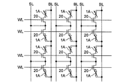
次に、本発明の第2実施形態による磁気メモリを図8乃至図13を参照して説明する。本実施形態に磁気メモリは、図8に示すようにマトリクス状に配列された複数のメモリセルを有し、各メモリセルは、磁気抵抗素子1Aと、選択トランジスタ20と、列毎に設けられたビット線BLおよびソース線SLと、行毎に設けられたワード線WLとを備えている。磁気抵抗素子1の一端は対応する列のビット線BLに接続され、他端は同じメモリセルの選択トランジスタ20のドレインに接続される。選択トランジスタ20のゲートは対応する行のワード線WLに接続される。また、同一列の隣接する2組のメモリセルの選択トランジスタ20のソースが共通に接続されて、対応する列のソース線SLに接続される。
(Second Embodiment)
Next, a magnetic memory according to a second embodiment of the present invention will be described with reference to FIGS. The magnetic memory in this embodiment has a plurality of memory cells arranged in a matrix as shown in FIG. 8, and each memory cell is provided for each column of the
本実施形態の磁気メモリに係る磁気抵抗素子1Aの断面を図9に示し、上からみた平面図を図10に示す。
FIG. 9 shows a cross section of the
基板40に選択トランジスタ20等が形成され、この選択トランジスタ20に一端が接続されたプラグ45が設けられている。そして、磁気抵抗素子1Aは、プラグ45の他端に接続される下部電極2と、下部電極2上に形成される反強磁性層4と、反強磁性層4上に形成される磁化固着層6と、磁化固着層6上に形成される第1トンネルバリア層8と、第1トンネルバリア層8上に形成される磁化自由層(記憶層)10と、磁化自由層10上に形成される第2トンネルバリア層12と、第2トンネルバリア層12上に形成されるキャップ層(図示せず)と、このキャップ層上に形成される上部電極14とを備えている。磁化自由層10から上部電極14までの積層膜は、下部電極2から第1トンネルバリア層8までの積層膜よりも膜面面積が小さくなるように構成されている。また、上部電極14は、対応するビット線BLに接続されている。また、本実施形態においては、図10に示すように、磁化自由層10とプラグ45とのそれぞれの中心を結ぶ線は、ビット線BLまたは磁化固着層6の長軸方向に平行となっている。
A
本実施形態に係る磁気抵抗素子1Aは、以下のように形成される。
The
まず、基板40に選択トランジスタ20等を形成し、この選択トランジスタ20に一端が接続されたプラグ45を設ける。続いて、プラグ45の他端に接続される下部電極2として膜厚が10nmのTa層と、反強磁性層4として膜厚20nmのPtMn層と、磁化固着層6として膜厚2nmCoFe層と膜厚0.6nmのRu層と膜厚2nmのCoFe層とからなる積層膜と、第1トンネルバリア層8として膜厚0.7nmのMgO層、磁化自由層10として膜厚2nmのCoFe層と、第2トンネルバリア層12として膜厚0.55nmのアルミナ層と、キャップ層(図示せず)として膜厚5nmのTa層と、上部電極14として膜厚60nmのTa層とを順次積層する。なお、アルミナ層12はAlを0.42nm堆積したのち、真空中で酸素ラジカルを用いてAlを酸化させることにより形成する。続いて、磁化固着層6の磁化を固着させるため、磁界中において330℃でアニールを行った。
First, the
次に、図11(a)に示すように、フォトリソグラフィー技術を用い、上部電極14から磁化自由層10までを100nm×150nmの所定の形状に加工する。このときの磁化自由層の長辺方向は図10に示すように磁化固着層の磁化の固着方向と平行にする。この後、保護膜16として膜厚30nmのSiNを堆積し、続いてフォトリソグラフィー技術を用い、保護膜16から下部電極2までを所定の形状に加工する。下部電極2の形状も、少しでも磁化固着層6の磁気異方性を高めるために、下部電極2の長辺を磁化固着層6の磁化の方向と平行にし、形状異方性を利用するとよい。磁化固着層6の異方性を強めることで磁化固着層6の磁化の擾乱を抑制することができ、反転電流を低減させることができる。
Next, as shown in FIG. 11A, the
次に、図11(b)に示すように、層間絶縁膜としてSiO2からなる絶縁膜(図示せず)を全面に堆積した後、CMP(Chemical Mechanical Polishing)を用いて、平坦化を施し、上部電極14の上面を露出させる。続いて、ビット線として、膜厚10nmのTi層、膜厚400nmのAl層、膜厚10nmのTi層、膜厚10nmのTiN層を順次積層して、所定の形状に加工することによりビット線BLを形成する(図11(c)参照)。その後、磁気抵抗素子を保護する保護膜や、ボンディング用の電極等を形成する。
Next, as shown in FIG. 11B, after an insulating film (not shown) made of SiO 2 is deposited on the entire surface as an interlayer insulating film, planarization is performed using CMP (Chemical Mechanical Polishing), The upper surface of the
本実施形態においては、第1トンネルバリア層8の面積規格化抵抗は10Ω/μm2、第2トンネルバリア層12の面積規格化抵抗は10Ω/μm2である。
In the present embodiment, the area normalized resistance of the first
参考までに、トンネルバリア層の材料がMgOとアルミナ(Al2O3)の場合のトンネルバリア層の厚さ(nm)と面積規格化抵抗Ra(Ω/μm2)の関係を図12に示す。界面の磁性体の酸化等の影響で多少のバラツキが生じる。特にAl2O3は上述のように、Alを堆積させた後、酸化することでAl2O3からなるバリアトンネル層を形成しているため、酸化工程の条件によっては大きく変化する。これに対して、MgOからなるトンネルバリア層は直接MgOを堆積することによって形成されるため、比較的安定している。 For reference, the relationship between the thickness (nm) of the tunnel barrier layer and the area normalized resistance Ra (Ω / μm 2 ) when the material of the tunnel barrier layer is MgO and alumina (Al 2 O 3 ) is shown in FIG. . Some variation occurs due to the influence of oxidation of the magnetic substance at the interface. In particular, since Al 2 O 3 is oxidized after depositing Al as described above to form a barrier tunnel layer made of Al 2 O 3 , it greatly varies depending on the conditions of the oxidation process. On the other hand, since the tunnel barrier layer made of MgO is formed by directly depositing MgO, it is relatively stable.
本実施形態に係る磁気抵抗素子の場合、書き込みに必要な電圧は、正および負の電圧でおおよそ0.4Vであった。読み出しをする際に、ある程度実用的な速度で読み出しを行おうとすると、回路的な容量時定数や感度の問題で、磁気抵抗素子にかける電圧を0.1V以上に設定する必要がある。一方、書き込みと読み出しは同じ電流経路であるため、読み出し時に磁気抵抗素子が誤書き込みされないためには、磁気抵抗素子のバラツキにもよるが、最低でも読み出しの3倍以上の電圧で書き込みできるように設計する必要がある。これらの制限から、書き込み電圧は0.4V以上で設計する必要がある。 In the case of the magnetoresistive element according to the present embodiment, the voltage required for writing is approximately 0.4 V for positive and negative voltages. At the time of reading, if reading is to be performed at a somewhat practical speed, it is necessary to set the voltage applied to the magnetoresistive element to 0.1 V or more due to problems of circuit capacity time constant and sensitivity. On the other hand, since writing and reading use the same current path, in order for the magnetoresistive element not to be erroneously written during reading, depending on variations in the magnetoresistive element, writing can be performed at a voltage at least three times that of reading. Need to design. Due to these limitations, it is necessary to design the write voltage at 0.4 V or higher.
0.4Vの書き込み電圧で書き込みをする際、擾乱を大きくするために与える0.08V以上の電圧(図6参照)を二つのトンネルバリア層に分配するには、第1トンネルバリア層8と第2トンネルバリア層のそれぞれの抵抗比は1:0.25〜1:4の範囲に設定することが必要となる。これは、図12に示す傾向から算出すると、トンネルバリア層8、12が同じ材料でかつそれぞれのトンネル接合の面積が実質的に同じである場合(例えば、第1実施形態の磁気抵抗効果素子の場合)、二つのトンネルバリア層の膜厚の差を0.14nm以内に設定することになる。0.14nmは、以下のように導かれる。MgOのRa(Ω/cm2)と膜厚dとの関係は、図12から、近似式として、
log(Ra)= 4.18×d−2.09
すなわち、 Ra=104.18×d−2.09
が得られる。ここで、二つのトンネル接合の面積が同じ場合、抵抗比はRaの比となる。第1トンネルバリア層8の膜厚をd1、第2トンネルバリア層12の膜厚をd2とすると、
104.18×d1−2.09/104.18×d2−2.09=1/4
となる。すなわち、
104.18×(d1−d2)=1/4
となり、
d1−d2≒0.14
が得られる。
本実施形態に係る磁気抵抗素子1Aは、第1実施形態と同様に、磁化自由層の両側にトンネルバリア層を備える構成を有しているので、正負どちらの電流方向においても磁化自由層にトンネルバリア層を介して、高エネルギーの電子を注入することが可能となり、磁化反転の際の反転電流をより低減することができる。
In order to distribute a voltage of 0.08 V or more (see FIG. 6), which is given to increase the disturbance, to the two tunnel barrier layers when writing with a write voltage of 0.4 V, the first
log (Ra) = 4.18 × d−2.09
That is, Ra = 10 4.18 × d−2.09
Is obtained. Here, when the area of the two tunnel junctions is the same, the resistance ratio is the ratio of Ra. If the film thickness of the first
10 4.18 × d1-2.09 / 10 4.18 × d2-2.09 = 1/4
It becomes. That is,
10 4.18 × (d1−d2) = 1/4
And
d1-d2≈0.14
Is obtained.
Since the
また、本実施形態においては、前述したように、磁化自由層10とプラグ45とのそれぞれの中心を結ぶ線は、ビット線BLまたは下部電極2の長軸方向に平行となっている(図10参照)。しかし、図13の平面図に示すように、磁化自由層10とプラグ45とのそれぞれの中心を結ぶ線は、ビット線BLまたは磁化固着層6の長軸方向(磁化固着層6の磁化の方向)に対して傾けることにより、
磁化固着層6と下部電極2に流れる電流磁界が磁化自由層10の磁化反転を助けることができる。例えば、図13に示すような構成にすることにより、ビット線BLに正の電圧を印加し、ビット線BLから電流を、磁気抵抗素子1Aを介してプラグ45に流すと、図13の矢印に示す方向に主に電流が流れる。この電流によって下部電極2上に生じる磁界の向きは、矢印の方向となる。元々スピン角運動量移動による反転を引き起こす力は、基本的に磁気抵抗素子内で無秩序な方向の力であるため、効率が悪いことが知られている。したがって、上記矢印の方向の磁界によって磁化自由層10の磁化の方向と90度直交する磁界の成分が生じ、この成分によって磁化自由層10の磁化方向と90度直交する磁界をアシストすることで、反転する際の方向が揃い、反転電流を下げることが可能となる。ここで重要なことは磁化自由層10の磁化の方向と90度直交する磁界をアシストすることである。図13に示すように磁気抵抗素子の中心(図13では、磁化自由層10の中心)と下部のトランジスタにつなぐためのプラグ45の中心とを結ぶ線を、磁化固着層の磁化の方向に対して傾ける角度は、本発明者達の実験によれば、0度〜45度が好ましかった。上記のように作製した磁気抵抗素子は、反転電流が低減し、バラツキも少なく、メモリとして良好に動作させることができた。
In the present embodiment, as described above, the line connecting the centers of the magnetization
The current magnetic field flowing through the magnetization pinned
(第3実施形態)
次に、本発明の第3実施形態による磁気メモリを、図14乃至図17(b)を参照して説明する。本実施形態の磁気メモリは、第2実施形態の磁気メモリと基本的な構成が同じであるため、変更した部分のみ説明する。大きく変更した部分は二点である。第1の点は、磁気抵抗素子の第2トンネルバリア層12の材料としてMgOを用いたこと、第2の点は、磁気抵抗素子の微細化を行ったことである。
(Third embodiment)
Next, a magnetic memory according to a third embodiment of the present invention will be described with reference to FIGS. 14 to 17B. Since the basic configuration of the magnetic memory of the present embodiment is the same as that of the magnetic memory of the second embodiment, only the changed part will be described. There are two major changes. The first point is that MgO is used as the material of the second
磁化自由層10の堆積までは第2実施形態と同様に行う。磁化自由層として膜厚2nmのCoFe層を堆積させた後、第2トンネルバリア層13として、膜厚0.6nmのMgO層を堆積し、引き続き第2実施形態と同様にキャップ層を堆積し、その後、第1上部電極14として膜厚15nmのTa層を積層した。一般的に金属の微細加工は難しく、その原因はRIE(Reactive Ion Etching)での加工時、反応生成物が磁気抵抗素子の側壁等に再付着し、形状にテーパーが生じサイズが大きくなることが原因である。そのため、微細加工するTaの膜厚をできるだけ薄くすることが重要となる。また、磁化固着層6の磁化を固着させるための磁界中アニールは360℃で行った。
The process up to the deposition of the magnetization
続いて、上部電極14から磁化自由層10までをフォトリソグラフィー技術を用いて40nm×60nmのサイズに加工した。その後、図14(a)に示すように保護膜16として膜厚20nmのSiN層を堆積し、続いて層間絶縁膜(図示せず)として膜厚20nmSiO2層を堆積した。本実施形態では、第1上部電極14から第1トンネルバリア層8までの段差hは高々15nm程度であり、平坦化して第1上部電極14の上面を露出するためには、段差の2倍以上絶縁膜を堆積することが望ましい。堆積膜の膜厚が大きくなると、第1上部電極14の上面を露出させるまでの研磨量が大きくなり、研磨不足、過剰等、製造上のバラツキにより歩留まりが低下する。このため、本実施形態では、SiN、SiO2の合計膜厚を段差hの2倍強とした。
Subsequently, the
続けて、CMPにより平坦化を行うが、通常のSiO2用のスラリーでは研磨速度が速く、今回のような精度が必要な研磨に不向きなため、本実施形態では、SiO2、Ta、SiNの研磨レートがおおよそ同程度である、Ta用のスラリーを用いて研磨を行った。本実施形態での研磨レートはSiO2でおおよそ、20nm/分であるため、おおよそ1.5分研磨することで、上部電極14の上面を露出することができた(図14(b)参照)。
Subsequently, planarization is performed by CMP. However, in the present embodiment, since a normal SiO 2 slurry has a high polishing rate and is not suitable for polishing that requires accuracy as in this case, in this embodiment, SiO 2 , Ta, and SiN are used. Polishing was performed using a Ta slurry having a polishing rate of approximately the same level. Since the polishing rate in this embodiment is approximately 20 nm / min with SiO 2 , the upper surface of the
しかる後、図14(c)に示すように、第2上部電極15として膜厚80nmのTa層を堆積し、フォトリソグラフィー技術を用い所定の形状に加工する。その後、第2上部電極15をマスクとして、下部電極2までエッチング除去し、自己整合的に下部電極2を所定の形状に加工し、本実施形態に係る磁気抵抗素子1Bを形成した(図15(a)参照)。
Thereafter, as shown in FIG. 14C, a Ta layer having a thickness of 80 nm is deposited as the second
続けて、図15(b)に示すように、層間絶縁膜18を堆積し、CMP工程で第2上部電極15の上面を露出させる。その後、膜厚10nmのTi層、膜厚400nmのAl層、膜厚10nmのTi層、膜厚10nmのTiN層を積層し、所定の形状に加工して、ビット配線BLを形成する。
Subsequently, as shown in FIG. 15B, an
第2実施形態の第2の点のポイントは、磁化自由層10を微細加工するために上部電極14の厚さを薄く設定することと、CMP工程での最初の第1上部電極14の露出工程を、他の段差がない、言い換えれば、下部電極2の加工前に行うことが肝心となる。その他の工程は適時、変更して作製することができる。例えば、第2上部電極15の上面の露出は、CMPによる平坦化ではなく、磁化自由層10のサイズより大きく加工した第2上部電極15へのビアを層間絶縁膜に形成することでもかまわない。
The second point of the second embodiment is that the thickness of the
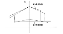
こうして作製した、磁気抵抗素子の特性を調べたところ、第3実施形態に係る磁気抵抗素子1Bの特性(実線で示す)は、図16に示すように第2実施形態に係る磁気抵抗素子1Aの特性(破線で示す)よりも電流をビット線からプラグ側に流した場合(正の電流を流した場合)の反転電流が低減していることが判った。この現象を詳しく調査したところ、この現象は、磁化自由層の上側の第2トンネルバリア層13にMgOを用いたことに起因することがわかった。
When the characteristics of the magnetoresistive element thus manufactured were examined, the characteristics (indicated by a solid line) of the
論文(W.H.Butler et al.,PHYSICAL REVIEW B, VOLUME 63,054416)に示されるように、CoFe系の磁性層とMgOを積層にした場合、電子が供給される磁性体内のマジョリティーのスピンとトンネル先の磁性体のマジョリティーのスピンが同方向の場合の電子のトンネル透過率が高いことが論じられている(図17(a)参照)。しかしながら、トンネル先の金属が非磁性の場合の効果については触れられていない。本実施形態に関連した実験によると図17(b)に示すように、電子を供給する磁性層のマジョリティーの電子スピンの透過率が、トンネル先が非磁性であっても高いことが新たにわかった。 As shown in the paper (WHButler et al., PHYSICAL REVIEW B, VOLUME 63,054416), when a CoFe-based magnetic layer and MgO are stacked, the spin of the majority in the magnetic body to which electrons are supplied and the tunnel destination It has been argued that the electron tunneling transmittance is high when the majority spins of the magnetic material are in the same direction (see FIG. 17A). However, no mention is made of the effect when the tunnel destination metal is non-magnetic. According to an experiment related to this embodiment, as shown in FIG. 17B, it is newly found that the majority electron spin transmittance of the magnetic layer supplying electrons is high even if the tunnel destination is non-magnetic. It was.
上記現象は、磁性体が金属の非磁性体と接触する場合、磁性体は非磁性体とスピン電子を交換しあう。そうすると界面近傍の磁性体のスピン偏極率が低下し、磁性体から出て行くスピンの偏極率を下げている可能性がある。金属に比べ、抵抗が高く(すなわち、電子のやりとりの少ない)、結晶系を揃えたMgOは、界面近傍の磁性体を劣化させず、高い偏極率の電子を磁性体から放出するのによい。 In the above phenomenon, when a magnetic material comes into contact with a metal nonmagnetic material, the magnetic material exchanges spin electrons with the nonmagnetic material. Then, there is a possibility that the spin polarization rate of the magnetic material in the vicinity of the interface is lowered, and the polarization rate of the spin coming out of the magnetic material is lowered. Compared to metals, MgO has higher resistance (that is, less exchange of electrons) and has a uniform crystal system, so it does not deteriorate the magnetic material near the interface and is good for emitting electrons with a high polarization rate from the magnetic material. .
したがって、本実施形態の構造において、トンネルバリア層13にMgOを用いた場合、磁化固着層6と磁化自由層10の磁化の向きがお互いに反平行(逆の向き)の場合に、電流を上部電極14から下部電極2の方向、すなわち電子が磁化固着層6から磁化自由層10に注入される場合、磁化固着層6から磁化自由層10に対して、磁化自由層10をより擾乱させるエネルギーを持った反対方向のスピンを持った電子が注入される。反転するまでは、主に注入される電子と反対のスピンを持った電子がマジョリティーであるから、磁化自由層10から上部電極14にはMgOからなるトンネルバリア層13を介して、磁化固着層6から主に注入される電子と逆のスピンを持った電子が選択的に通過する。結果として、磁化固着層6からのエネルギーを持った逆向きのスピンの注入と上部電極14への磁化自由層10のマジョリティースピンの透過によって、磁化自由層10が反転することになる。なお、上記、効果を顕著にするためには、トンネルバリア層13のMgOは、<100>方向へ優先配向させることで効果をより大きくできることがわかった。
Therefore, in the structure of the present embodiment, when MgO is used for the
以上説明したように、本実施形態によれば、磁化反転の際の反転電流をより低減することができる。さらに、第2実施形態の場合と同様に、図13に示すような構成とすることにより、バラツキも少なく、メモリとして良好に動作させることができた。 As described above, according to this embodiment, the reversal current at the time of magnetization reversal can be further reduced. Further, as in the case of the second embodiment, by adopting the configuration as shown in FIG. 13, there was little variation and the memory could be operated satisfactorily.
(第4実施形態)
本発明の第4実施形態の磁気抵抗素子を、図18を参照して説明する。第1乃至第3実施形態に係る磁気抵抗素子は、磁化固着層6および磁化自由層10の磁化の方向は、膜面に平行であった。これに対して本実施形態の磁気抵抗素子は、磁化固着層6Aおよび磁化自由層10Aとして、磁化の方向を膜面に対して垂直な方向へ磁化させたいわゆる垂直磁化材料を用いた構成となっている。したがって、本実施形態の磁気抵抗素子は、下部電極2と、磁化固着層6Aと、第1トンネルバリア層8と、磁化自由層10Aと、第2トンネルバリア層13と、上部電極14を備えており、第1乃至第3実施形態に係る磁気抵抗素子とは反強磁性層を備えていない点で異なっている。
(Fourth embodiment)
A magnetoresistive element according to a fourth embodiment of the present invention will be described with reference to FIG. In the magnetoresistive element according to the first to third embodiments, the magnetization directions of the magnetization fixed
本実施形態の磁気抵抗素子は、以下のように形成される。まず、選択トランジスタ等を形成した基板上に、下部電極2として膜厚が10nmのTa層と、CrTi系合金からなる膜厚20nmのバッファー層(図示せず)と、磁化固着層6Aとして膜厚5nmのFePt層と、第1トンネルバリア層8として膜厚0.7nmのMgO層と、磁化自由層10Aとして膜厚が1nmのFe層および膜厚が3nmのFePt層の積層膜と、第2トンネルバリア層13として膜厚が0.6nmのMgO層を順次堆積し、その後、キャップ層兼上部電極14として、膜厚が80nmのTi層を積層した後、磁化固着層、磁化自由層を垂直方向へ磁化させるために、400℃で規則化アニールを行い、第1乃至第3実施形態と同様に磁気抵抗素子を完成させた。なお、本実施形態においては、磁化の方向は膜面に垂直であるので、磁化固着層6Aの磁化の向きを固着する磁性材料が存在しない。このため、磁化固着層6Aの磁化の固着は行わず、保持力差をつけるため、磁化自由層10Aに対して磁化固着層6Aの磁化容易軸方向の保持力Hcおよび磁化困難軸方向の保持力Hkを大きくしている。
The magnetoresistive element of this embodiment is formed as follows. First, a Ta layer having a thickness of 10 nm as a
本実施形態の磁気抵抗素子も、第1実施形態と同様に、磁化自由層の両側にトンネルバリア層を備える構成を有しているので、正負どちらの電流方向においても磁化自由層にトンネルバリア層を介して、高エネルギーの電子を注入することが可能となり、磁化反転の際の反転電流をより低減することができる。 Similarly to the first embodiment, the magnetoresistive element of the present embodiment has a configuration including tunnel barrier layers on both sides of the magnetization free layer. Therefore, the tunnel barrier layer is included in the magnetization free layer in both positive and negative current directions. Thus, it becomes possible to inject electrons with high energy, and the reversal current at the time of magnetization reversal can be further reduced.
(第5実施形態)
次に、本発明の第5実施形態による磁気抵抗素子を説明する。本実施形態の磁気抵抗素子は、第4実施形態の磁気抵抗素子とは、磁化固着層6Aおよび磁化自由層10Aの垂直磁化材料が異なっている。本実施形態の磁気抵抗素子は以下の構成となっている。選択トランジスタ等を形成した基板上に、下部電極として膜厚が10nmのTa層と、TbCoFe系合金からなる膜厚が10nmの磁化固着層と、界面層として膜厚1nmのCo層と、第1トンネルバリア層として膜厚が0.7nmのMgO層、磁化自由層として膜厚が1nmのCo層および膜厚が3nmのTbCoFe層との積層膜と、第2トンネルバリア層として膜厚0.6nmのMgO層と、を堆積し、続いて、キャップ層兼上部電極として膜厚が80nmのTi層を積層し、以降は第4実施形態例と同様に磁気抵抗素子を完成させた。
(Fifth embodiment)
Next, a magnetoresistive element according to a fifth embodiment of the invention will be described. The magnetoresistive element of the present embodiment is different from the magnetoresistive element of the fourth embodiment in the perpendicular magnetization materials of the magnetization fixed
本実施形態の磁気抵抗素子も、第1実施形態と同様に、磁化自由層の両側にトンネルバリア層を備える構成を有しているので、正負どちらの電流方向においても磁化自由層にトンネルバリア層を介して、高エネルギーの電子を注入することが可能となり、磁化反転の際の反転電流をより低減することができる。 Similarly to the first embodiment, the magnetoresistive element of the present embodiment has a configuration including tunnel barrier layers on both sides of the magnetization free layer. Therefore, the tunnel barrier layer is included in the magnetization free layer in both positive and negative current directions. Thus, it becomes possible to inject electrons with high energy, and the reversal current at the time of magnetization reversal can be further reduced.
(第6実施形態)
次に、本発明の第6実施形態による磁気抵抗素子を説明する。本実施形態の磁気抵抗素子は、スピントルクを発生する第1トンネルバリア層の面積を大きくした構成となっている。磁化自由層(記憶層)にCoFe(B)やNiFe等の軟磁性材料を用いたスピン注入型の磁気抵抗素子の場合、スイッチング電流は、磁気抵抗素子の熱擾乱耐性を表す熱擾乱指数に比例する。したがって、磁気抵抗素子に必要な熱擾乱指数が決まると電流がおのずと決まる。
(Sixth embodiment)
Next, a magnetoresistive element according to a sixth embodiment of the invention will be described. The magnetoresistive element of this embodiment has a configuration in which the area of the first tunnel barrier layer that generates spin torque is increased. In the case of a spin-injection magnetoresistive element using a soft magnetic material such as CoFe (B) or NiFe for the magnetization free layer (memory layer), the switching current is proportional to the thermal disturbance index representing the thermal disturbance resistance of the magnetoresistive element. To do. Accordingly, when the thermal disturbance index required for the magnetoresistive element is determined, the current is naturally determined.
一方、トンネルバリア層の耐性を考えると、トンネルバリア層に流す電流密度は小さい程よく、同じ電流を流すなら、トンネルバリア層の面積を大きくした方が信頼性上、有利となる。しかし、通常の方法では、トンネルバリア層の面積は磁性体の面積と同じになり、同じ熱擾乱指数を保ったまま(すなわち、スイッチング電流を保ったまま)面積を大きくするためには、磁性体の膜厚を減らさなければならない。また、磁化固着層および磁化自由層の磁化の方向は、磁性体の形状によって誘起された形状異方性を利用しているため、形状に制限もある。本発明者達が用いたCoFeからなる磁性材料の場合、膜厚が1.5nmよりも小さくなると良好な形状異方性が発生せず、良好なヒステリシス特性を示さなくなった。 On the other hand, considering the resistance of the tunnel barrier layer, the current density flowing through the tunnel barrier layer is preferably as small as possible. If the same current is supplied, it is advantageous in terms of reliability to increase the area of the tunnel barrier layer. However, in the normal method, the area of the tunnel barrier layer is the same as the area of the magnetic body, and in order to increase the area while maintaining the same thermal disturbance index (ie, maintaining the switching current), the magnetic body The film thickness must be reduced. Further, the magnetization directions of the magnetization pinned layer and the magnetization free layer are limited in shape because they utilize shape anisotropy induced by the shape of the magnetic material. In the case of the magnetic material made of CoFe used by the present inventors, when the film thickness is smaller than 1.5 nm, good shape anisotropy does not occur, and good hysteresis characteristics are not exhibited.
本実施形態では、このような問題を解決できる構成となっている。以下、本実施形態の磁気抵抗素子の製造方法を図19(a)乃至図21を参照して説明する。 In the present embodiment, such a problem can be solved. Hereinafter, the manufacturing method of the magnetoresistive element of the present embodiment will be described with reference to FIGS.
まず、図19(a)に示すように、選択トランジスタ等を形成した基板(図示せず)上に、膜厚が10nmのTaからなる下部電極2と、PtMnからなる膜厚が20nmの反強磁性層4と、膜厚が2nmのCoFe層、膜厚が0.6nmのRu層、および膜厚が2nmのCoFe層の積層構造の磁化固着層6と、MgOからなる膜厚が0.8nmの第1トンネルバリア層8と、CoFeからなる膜厚が1.5nmの第1磁化自由層101と、NiFeからなる膜厚が6nmの第2磁化自由層102と、CoFeからなる膜厚が1nmの界面層(図示せず)と、MgOからなる膜厚が0.6nmの第2トンネルバリア層13と、を順次形成し、続いて、Taからなる膜厚が60nmの上部電極14を形成する。この後、磁化固着層6の磁化の向きを固着し、磁化固着層6と、第1トンネルバリア層との界面のCoFe層の結晶性を向上させるため、磁界中において360℃でアニールを行った。
First, as shown in FIG. 19A, on a substrate (not shown) on which a selection transistor or the like is formed, a
その後、フォトリソグラフィー技術を用いて、まず上部電極14から第2磁化自由層102までを30nm×100nmの所定の形状に加工する(図19(b)参照)。続いて、図19(c)に示すように、保護膜20として膜厚が30nmのSiN膜を堆積し、その後、フォトリソグラフィー技術を用いて、保護膜20から第1磁化自由層101までを所定の形状に加工する。
Then, using photolithography, firstly processing the
次に、図20(a)に示すように、保護膜22として膜厚が30nmのSiN膜を堆積し、フォトリソグラフィー技術を用いて保護膜22から下部電極2までを所定の形状に加工する。
Next, as shown in FIG. 20A, an SiN film having a thickness of 30 nm is deposited as the
次に、図20(b)に示すように、SiO2からなる層間絶縁膜24を形成したのち、CMPを用いて、平坦化を施し、上部電極14の上面を露出させる。この後、図20(c)に示すように、ビット線BLとして膜厚が10nmのTi層、膜厚が400nmのAl層、膜厚が10nmのTi層、膜厚が10nmのTiN層を積層し、所定の形状に加工して、磁気抵抗素子を完成する。
Next, as shown in FIG. 20B, after an
本実施形態での、第1磁化自由層101と第2磁化自由層102の平面図を図21に示す。第1磁化自由層101はある程度の形状異方性が誘起されるようにアスペクトをとっておくとよい。また、第2磁化自由層102は十分な形状異方性を付与させるために、アスペクトは3以上が望ましい。さらに、第1磁化自由層101と第2磁化自由層102は 磁化モーメントがおおよそ同じになるように設計するとよい。本実施形態の場合、第1磁化自由層101の磁化モーメントが1000emu/cc、第2磁化自由層102の磁化モーメント(界面層の磁化モーメントも含む)が800emu/ccであるので、比は17:15程度である。この場合、第1磁化自由層101が中間値等をとることなく、安定してスピン反転させることができた。また、第1磁化自由層101と第2磁化自由層102の膜面の面積比は4.8倍であるので、第1トンネルバリア層8に必要な電流密度を、例えば第1磁化自由層101と第2磁化自由層102の膜面面積が同一である場合に比べて、1/4.8にすることができ、信頼性が向上した。
FIG. 21 shows a plan view of the first magnetization
また、本実施形態の場合、MgOからなる第1トンネルバリア層8の膜厚は0.8nm、Raは約17.9Ω/μm2、面積は約0.0127μm2、MgOからなる第2トンネルバリア層13の膜厚は0.6nm、Raは約2.6Ω/μm2、面積は約0.00236μm2であるから、第1および第2トンネルバリア層8、13の抵抗値はそれぞれ1409Ω、1101Ωとなる。したがって、第1および第2トンネルバリア層8、13の抵抗値の比は1:0.79となる。すなわち、1:0.25〜4の範囲に入っている。
Further, in this embodiment, the thickness of the first
本実施形態の磁気抵抗素子も、第1実施形態と同様に、磁化自由層の両側にトンネルバリア層を備える構成を有しているので、正負どちらの電流方向においても磁化自由層にトンネルバリア層を介して、高エネルギーの電子を注入することが可能となり、磁化反転の際の反転電流をより低減することができる。 Similarly to the first embodiment, the magnetoresistive element of the present embodiment has a configuration including tunnel barrier layers on both sides of the magnetization free layer. Therefore, the tunnel barrier layer is included in the magnetization free layer in both positive and negative current directions. Thus, it becomes possible to inject electrons with high energy, and the reversal current at the time of magnetization reversal can be further reduced.
(第7実施形態)
次に、本発明の第7実施形態による磁気抵抗素子を図22(a)乃至図23(c)を参照して説明する。
(Seventh embodiment)
Next, a magnetoresistive element according to a seventh embodiment of the present invention will be described with reference to FIGS. 22 (a) to 23 (c).
本実施形態の磁気抵抗素子は、磁化自由層の熱擾乱耐性を軟磁気特性膜によって得た構成となっている。第4および第5実施形態では、材料の特性を活かして大きな垂直磁気異方性を利用して、微細化素子にして熱擾乱耐性を持たせることに対して、軟磁性体を用いた場合は、形状でほとんどの磁気特性を制御することができ、膜質のバラツキ等に左右されない、均一性の高い素子を作製することが可能である。ただし、大きな軟磁気特性膜で大きな磁気異方性を得るためには、出来るだけ大きな体積を有し、かつ形状異方性を利用するためにアスペクト比(膜面に平行な面における縦の長さ(紙面に垂直な方向の長さ)と横の長さ(紙面の左右方向の長さ)の比)の大きな形状にすることが望ましく、棒状が望ましい。本実施形態は以下の作製方法で磁化自由層を棒状に加工し、磁気抵抗素子を作製した。 The magnetoresistive element of this embodiment has a configuration in which the thermal disturbance resistance of the magnetization free layer is obtained by a soft magnetic property film. In the fourth and fifth embodiments, when a soft magnetic material is used for making a miniaturized element having thermal disturbance resistance by utilizing a large perpendicular magnetic anisotropy utilizing the characteristics of the material. Most of the magnetic characteristics can be controlled by the shape, and a highly uniform element that is not affected by variations in film quality or the like can be manufactured. However, in order to obtain a large magnetic anisotropy with a large soft magnetic property film, the aspect ratio (vertical length in a plane parallel to the film surface) has to be as large as possible and use the shape anisotropy. It is desirable to have a large shape (ratio of the length in the direction perpendicular to the paper surface) and the lateral length (length in the left-right direction of the paper surface), and a rod shape is desirable. In this embodiment, the magnetoresistive element was manufactured by processing the magnetization free layer into a rod shape by the following manufacturing method.
まず、図22(a)に示すように、選択トランジスタ等を形成した基板上に、膜厚が10nmのTaからなる下部電極2と、膜厚が20nmのPtMnからなる反強磁性層4と、膜厚が2nmのCoFe層、膜厚が0.6nmのRu層、および膜厚が2nmのCoFe層の積層構造を有する磁化固着層6と、膜厚が0.7nmのMgOからなる第1トンネルバリア層8と、膜厚が1.5nmのCoFeからなる第1磁化自由層10を順次堆積する。続いて図22(b)に示すように、膜厚が30nmのSiNからなる保護膜26を堆積し、フォトリソグラフィー技術を用いて保護膜26を平面形状として30nm×100nmの溝状に加工する。このとき、レジスト剥離工程で、露出した下地のCoFeからなる第1磁化自由層10を酸化させないようにする。
First, as shown in FIG. 22A, a
図22(c)に示すように、溝にNiFeをスパッタリング等で埋め込み、図22(c)に示すようにCMPを用いて、NiFeを棒状に加工する。このとき、棒状に加工されたNiFe膜28の膜厚は20nmとなるようにCMPを用いて調整した。この棒状に加工されたNiFe膜28は第2磁化自由層となり、第1磁化自由層10よりも幅(磁化困難軸方向(紙面の左右方向)の長さ)が狭い。
As shown in FIG. 22C, NiFe is buried in the groove by sputtering or the like, and as shown in FIG. 22C, NiFe is processed into a rod shape using CMP. At this time, the thickness of the
次に、図23(a)に示すように、膜厚1.5nmのCoFeからなる界面層30、膜厚0.6nmのMgOからなる第2トンネルバリア層13、膜厚が80nmのTaからなる上部電極14を順次堆積する。しかる後に、図23(b)に示すように、上部電極14から、下部電極2までを所定の形状に加工した。
Next, as shown in FIG. 23A, the
次に、図23(c)に示すように、SiO2からなる層間絶縁膜32を形成した後、CMPを用いて層間絶縁膜32を平坦化し、上部電極14の上面を露出させる。続いて、膜厚10nmのTi層、膜厚400nmのAl層、膜厚10nmのTi層、膜厚10nmのTiN層を順次積層し、所定の形状に加工することによりビット線BLを形成し、磁気抵抗素子を完成する。
Next, as shown in FIG. 23C, after an
本実施形態の磁気抵抗素子も、第1実施形態と同様に、磁化自由層の両側にトンネルバリア層を備える構成を有しているので、正負どちらの電流方向においても磁化自由層にトンネルバリア層を介して、高エネルギーの電子を注入することが可能となり、磁化反転の際の反転電流をより低減することができる。 Similarly to the first embodiment, the magnetoresistive element of the present embodiment has a configuration including tunnel barrier layers on both sides of the magnetization free layer. Therefore, the tunnel barrier layer is included in the magnetization free layer in both positive and negative current directions. Thus, it becomes possible to inject electrons with high energy, and the reversal current at the time of magnetization reversal can be further reduced.
なお、第4乃至第7実施形態の磁気抵抗素子は、第2乃至第3実施形態の磁気メモリの磁気抵抗素子として用いることができることは云うまでもない。 Needless to say, the magnetoresistive elements of the fourth to seventh embodiments can be used as the magnetoresistive elements of the magnetic memories of the second to third embodiments.
1 磁気抵抗素子
1A 磁気抵抗素子
1B 磁気抵抗素子
2 下部電極
4 反強磁性層
6 磁化固着層
8 第1トンネルバリア層
10 磁化自由層(記憶層)
12 第2トンネルバリア層
13 第2トンネルバリア層
14 上部電極
DESCRIPTION OF
12 Second
Claims (14)
前記磁化自由層の磁化の向きは、前記磁化固着層と前記非磁性層との間で通電することにより変化可能であり、
前記第1トンネルバリア層と前記第2トンネルバリア層の抵抗比が1:0.25〜1:4の範囲にあり、
前記磁化自由層は、前記第1トンネルバリア層側に設けられた第1軟磁性層と、前記第2トンネルバリア層側に設けられ前記第1軟磁性層よりも膜面の面積が狭い第2軟磁性層とを備えていることを特徴とする磁気抵抗素子。 A magnetization free layer having a first surface and a second surface opposite to the first surface and having a variable magnetization direction, and provided on the first surface side of the first surface and the second surface of the magnetization free layer. A magnetization fixed layer in which the magnetization direction is fixed; a first tunnel barrier layer provided between the magnetization free layer and the magnetization fixed layer; and a second tunnel provided on a second surface of the magnetization free layer A barrier layer, and a nonmagnetic layer provided to be in contact with a surface of the second tunnel barrier layer opposite to the magnetization free layer,
The magnetization direction of the magnetization free layer can be changed by energization between the magnetization pinned layer and the nonmagnetic layer,
Resistance ratio of the first tunnel barrier layer and the second tunnel barrier layer is 1: 0.25 to 1: Ri range near 4,
The magnetization free layer includes a first soft magnetic layer provided on the first tunnel barrier layer side and a second soft magnetic layer provided on the second tunnel barrier layer side and having a film surface area smaller than that of the first soft magnetic layer. A magnetoresistive element comprising a soft magnetic layer .
前記磁化自由層の磁化の向きは、前記磁化固着層と前記非磁性層との間で通電することにより変化可能であり、
前記第1トンネルバリア層と前記第2トンネルバリア層の抵抗比が1:0.25〜1:4の範囲にあり、
前記磁化自由層は、前記第1トンネルバリア層側に設けられた第1軟磁性層と、前記第2トンネルバリア層側に設けられ前記第1軟磁性層よりも磁化困難軸方向の長さが狭い第2軟磁性層とを備えていることを特徴とする磁気抵抗素子。 A magnetization free layer having a first surface and a second surface opposite to the first surface and having a variable magnetization direction, and provided on the first surface side of the first surface and the second surface of the magnetization free layer. A magnetization fixed layer in which the magnetization direction is fixed; a first tunnel barrier layer provided between the magnetization free layer and the magnetization fixed layer; and a second tunnel provided on a second surface of the magnetization free layer A barrier layer, and a nonmagnetic layer provided to be in contact with a surface of the second tunnel barrier layer opposite to the magnetization free layer,
The magnetization direction of the magnetization free layer can be changed by energization between the magnetization pinned layer and the nonmagnetic layer,
Resistance ratio of the first tunnel barrier layer and the second tunnel barrier layer is 1: 0.25 to 1: Ri range near 4,
The magnetization free layer has a first soft magnetic layer provided on the first tunnel barrier layer side and a length in the hard axis direction than the first soft magnetic layer provided on the second tunnel barrier layer side. A magnetoresistive element comprising a narrow second soft magnetic layer .
前記磁気抵抗素子の一端に接続される第1配線と、
前記磁気抵抗素子の他端と電気的に接続される第2配線と、
を備えたことを特徴とする磁気メモリ。 A magnetoresistive element according to any one of claims 1 to 7,
A first wiring connected to one end of the magnetoresistive element;
A second wiring electrically connected to the other end of the magnetoresistive element;
A magnetic memory comprising:
前記磁気抵抗素子の一端に接続される第1配線と、
前記磁気抵抗素子の他端と電気的に接続される第2配線と、
前記磁気抵抗素子の他端と前記第2配線との間に設けられた選択トランジスタと、
前記磁気抵抗素子の他端と前記選択トランジスタとの間に膜面に実質的に垂直に延在する接続部と、
を有し、
前記磁気抵抗素子を上面からみたときに前記磁化自由層の中心と前記接続部の中心とを結ぶ直線は、前記磁化固着層の磁化の向きに対して傾いていることを特徴とする磁気メモリ。 A magnetization free layer having a first surface and a second surface opposite to the first surface and having a variable magnetization direction, and provided on the first surface side of the first surface and the second surface of the magnetization free layer. A magnetization fixed layer in which the magnetization direction is fixed; a first tunnel barrier layer provided between the magnetization free layer and the magnetization fixed layer; and a second tunnel provided on a second surface of the magnetization free layer A barrier layer, and a nonmagnetic layer provided so as to be in contact with a surface of the second tunnel barrier layer opposite to the magnetization free layer, and the magnetization direction of the magnetization free layer is different from that of the magnetization pinned layer and the magnetization fixed layer. A magnetoresistive element that can be changed by energizing between the nonmagnetic layer and the resistance ratio of the first tunnel barrier layer to the second tunnel barrier layer is in the range of 1: 0.25 to 1: 4. When,
A first wiring connected to one end of the magnetoresistive element;
A second wiring electrically connected to the other end of the magnetoresistive element;
A select transistor provided between the other end of the magnetoresistive element and the second wiring;
A connection portion extending substantially perpendicular to the film surface between the other end of the magnetoresistive element and the selection transistor;
Have
A magnetic memory characterized in that when the magnetoresistive element is viewed from above, a straight line connecting the center of the magnetization free layer and the center of the connection portion is inclined with respect to the magnetization direction of the magnetization pinned layer.
前記磁気抵抗素子の一端に接続される第1配線と、
前記磁気抵抗素子の他端と電気的に接続される第2配線と、
前記磁気抵抗素子の他端と前記第2配線との間に設けられた選択トランジスタと、
前記磁気抵抗素子の他端と前記選択トランジスタとの間に膜面に実質的に垂直に延在する接続部と、
を有し、
前記磁気抵抗素子を上面からみたときに前記磁化自由層の中心と前記接続部の中心とを結ぶ直線は、前記磁化固着層の磁化の向きに対して傾いていることを特徴とする磁気メモリ。 A magnetization free layer having a first surface and a second surface opposite to the first surface and having a variable magnetization direction, and provided on the first surface side of the first surface and the second surface of the magnetization free layer. A magnetization fixed layer in which the magnetization direction is fixed; a first tunnel barrier layer provided between the magnetization free layer and the magnetization fixed layer; and a second tunnel provided on a second surface of the magnetization free layer And a nonmagnetic layer provided so as to be in contact with a surface of the second tunnel barrier layer opposite to the magnetization free layer, the magnetization direction of the magnetization free layer being different from that of the magnetization pinned layer. When the first tunnel barrier layer and the second tunnel barrier layer are formed of the same material and the area of the tunnel junction is substantially equal, the first tunnel barrier layer and the second tunnel barrier layer can be changed by energizing the nonmagnetic layer. 2 tunnel barrier layers and the thickness of the first tunnel barrier layer The difference is less than 0.14 nm, a magnetoresistive element,
A first wiring connected to one end of the magnetoresistive element;
A second wiring electrically connected to the other end of the magnetoresistive element;
A select transistor provided between the other end of the magnetoresistive element and the second wiring;
A connection portion extending substantially perpendicular to the film surface between the other end of the magnetoresistive element and the selection transistor;
Have
A magnetic memory characterized in that when the magnetoresistive element is viewed from above, a straight line connecting the center of the magnetization free layer and the center of the connection portion is inclined with respect to the magnetization direction of the magnetization pinned layer.
Priority Applications (5)
| Application Number | Priority Date | Filing Date | Title |
|---|---|---|---|
| JP2007016930A JP4384183B2 (en) | 2007-01-26 | 2007-01-26 | Magnetoresistive element and magnetic memory |
| US12/014,522 US7894246B2 (en) | 2007-01-26 | 2008-01-15 | Magnetoresistive element and magnetic memory |
| CN200810008901A CN100592544C (en) | 2007-01-26 | 2008-01-25 | Magnetoresistive element and magnetic memory |
| KR1020080008296A KR20080070597A (en) | 2007-01-26 | 2008-01-25 | Magnetoresistive element and magnetic memory |
| US12/851,275 US8173447B2 (en) | 2007-01-26 | 2010-08-05 | Magnetoresistive element and magnetic memory |
Applications Claiming Priority (1)
| Application Number | Priority Date | Filing Date | Title |
|---|---|---|---|
| JP2007016930A JP4384183B2 (en) | 2007-01-26 | 2007-01-26 | Magnetoresistive element and magnetic memory |
Related Child Applications (1)
| Application Number | Title | Priority Date | Filing Date |
|---|---|---|---|
| JP2009107971A Division JP5058206B2 (en) | 2009-04-27 | 2009-04-27 | Method for manufacturing magnetoresistive element |
Publications (2)
| Publication Number | Publication Date |
|---|---|
| JP2008186861A JP2008186861A (en) | 2008-08-14 |
| JP4384183B2 true JP4384183B2 (en) | 2009-12-16 |
Family
ID=39667689
Family Applications (1)
| Application Number | Title | Priority Date | Filing Date |
|---|---|---|---|
| JP2007016930A Active JP4384183B2 (en) | 2007-01-26 | 2007-01-26 | Magnetoresistive element and magnetic memory |
Country Status (4)
| Country | Link |
|---|---|
| US (2) | US7894246B2 (en) |
| JP (1) | JP4384183B2 (en) |
| KR (1) | KR20080070597A (en) |
| CN (1) | CN100592544C (en) |
Cited By (1)
| Publication number | Priority date | Publication date | Assignee | Title |
|---|---|---|---|---|
| US10964884B2 (en) | 2019-03-18 | 2021-03-30 | Toshiba Memory Corporation | Magnetic memory device having an incline side surface |
Families Citing this family (34)
| Publication number | Priority date | Publication date | Assignee | Title |
|---|---|---|---|---|
| JP4444241B2 (en) * | 2005-10-19 | 2010-03-31 | 株式会社東芝 | Magnetoresistive element, magnetic random access memory, electronic card and electronic device |
| JP5143444B2 (en) * | 2007-02-13 | 2013-02-13 | 株式会社日立製作所 | Magnetoresistive element, magnetic memory cell and magnetic random access memory using the same |
| JP2008205186A (en) * | 2007-02-20 | 2008-09-04 | Sony Corp | Storage cell and memory |
| JP4738395B2 (en) * | 2007-09-25 | 2011-08-03 | 株式会社東芝 | Magnetoresistive element and magnetic random access memory using the same |
| JP2009239121A (en) * | 2008-03-27 | 2009-10-15 | Toshiba Corp | Magnetoresistive element and magnetic random access memory |
| US7939188B2 (en) * | 2008-10-27 | 2011-05-10 | Seagate Technology Llc | Magnetic stack design |
| US8045366B2 (en) * | 2008-11-05 | 2011-10-25 | Seagate Technology Llc | STRAM with composite free magnetic element |
| JP2010135512A (en) * | 2008-12-03 | 2010-06-17 | Sony Corp | Resistance change memory device |
| WO2010067520A1 (en) * | 2008-12-10 | 2010-06-17 | 株式会社日立製作所 | Magnetoresistance effect element and magnetic memory cell and magnetic random access memory using same |
| JP2010182824A (en) * | 2009-02-04 | 2010-08-19 | Toshiba Corp | Method of manufacturing magnetic random access memory, and method of manufacturing embedded memory |
| JP2010232374A (en) * | 2009-03-26 | 2010-10-14 | Nippon Hoso Kyokai <Nhk> | Magnetoresistive element, and magnetic random access memory and spatial light modulator using the same |
| US8344433B2 (en) * | 2009-04-14 | 2013-01-01 | Qualcomm Incorporated | Magnetic tunnel junction (MTJ) and methods, and magnetic random access memory (MRAM) employing same |
| US8455267B2 (en) | 2009-05-14 | 2013-06-04 | Qualcomm Incorporated | Magnetic tunnel junction device and fabrication |
| WO2010143248A1 (en) * | 2009-06-08 | 2010-12-16 | 株式会社日立製作所 | Tunnel magnetic resistance effect element and random access memory using same |
| US8455965B2 (en) * | 2009-11-30 | 2013-06-04 | Qualcomm Incorporated | Fabrication and integration of devices with top and bottom electrodes including magnetic tunnel junctions |
| JP2011166015A (en) * | 2010-02-12 | 2011-08-25 | Renesas Electronics Corp | Semiconductor device and method of manufacturing the same |
| US8324697B2 (en) * | 2010-06-15 | 2012-12-04 | International Business Machines Corporation | Seed layer and free magnetic layer for perpendicular anisotropy in a spin-torque magnetic random access memory |
| JP2012015213A (en) * | 2010-06-29 | 2012-01-19 | Sony Corp | Storage element, manufacturing method thereof, and memory |
| JP2012064623A (en) * | 2010-09-14 | 2012-03-29 | Sony Corp | Storage element and memory unit |
| KR101463948B1 (en) * | 2010-11-08 | 2014-11-27 | 삼성전자주식회사 | Magnetic memory devices |
| CN102682840A (en) * | 2011-03-18 | 2012-09-19 | 中国科学院微电子研究所 | Method and structure for improving reliability of non-volatile resistive memory |
| US8767446B2 (en) * | 2011-10-12 | 2014-07-01 | International Business Machines Corporation | Multi-bit spin-momentum-transfer magnetoresistence random access memory with single magnetic-tunnel-junction stack |
| US9054030B2 (en) | 2012-06-19 | 2015-06-09 | Micron Technology, Inc. | Memory cells, semiconductor device structures, memory systems, and methods of fabrication |
| KR102017623B1 (en) | 2012-08-30 | 2019-09-03 | 삼성전자주식회사 | Magnetic Memory Device |
| JP2014203931A (en) | 2013-04-03 | 2014-10-27 | 株式会社東芝 | Magnetic memory, spin element, and spin mos transistor |
| CN103675094A (en) * | 2013-12-16 | 2014-03-26 | 无锡乐尔科技有限公司 | Non-destructive testing device |
| JP2015179779A (en) * | 2014-03-19 | 2015-10-08 | 株式会社東芝 | Strain detection element, pressure sensor, microphone, blood pressure sensor, and touch panel |
| JP2015213125A (en) * | 2014-05-02 | 2015-11-26 | 日本放送協会 | Spin injection magnetization reversal element |
| CN107578791B (en) * | 2016-07-04 | 2020-05-22 | 中国科学院物理研究所 | Spin torque oscillator with high output power and application thereof |
| CN106206935B (en) * | 2016-07-14 | 2019-01-04 | 华中科技大学 | A method of control spin wave transmission |
| KR20180016874A (en) * | 2016-08-08 | 2018-02-20 | 에스케이하이닉스 주식회사 | Electronic device and method for fabricating the same |
| US10564229B2 (en) * | 2017-10-16 | 2020-02-18 | Tdk Corporation | Tunnel magnetoresistive effect element, magnetic memory, and built-in memory |
| KR102470367B1 (en) * | 2017-11-24 | 2022-11-24 | 삼성전자주식회사 | Method of manufacturing a magnetoresistive random access device |
| KR20200142159A (en) | 2019-06-11 | 2020-12-22 | 삼성전자주식회사 | Magnetic memory device |
Family Cites Families (19)
| Publication number | Priority date | Publication date | Assignee | Title |
|---|---|---|---|---|
| US6130814A (en) * | 1998-07-28 | 2000-10-10 | International Business Machines Corporation | Current-induced magnetic switching device and memory including the same |
| US6178074B1 (en) * | 1998-11-19 | 2001-01-23 | International Business Machines Corporation | Double tunnel junction with magnetoresistance enhancement layer |
| US6611405B1 (en) * | 1999-09-16 | 2003-08-26 | Kabushiki Kaisha Toshiba | Magnetoresistive element and magnetic memory device |
| JP4693292B2 (en) * | 2000-09-11 | 2011-06-01 | 株式会社東芝 | Ferromagnetic tunnel junction device and manufacturing method thereof |
| JP3959335B2 (en) * | 2002-07-30 | 2007-08-15 | 株式会社東芝 | Magnetic storage device and manufacturing method thereof |
| US6958927B1 (en) * | 2002-10-09 | 2005-10-25 | Grandis Inc. | Magnetic element utilizing spin-transfer and half-metals and an MRAM device using the magnetic element |
| JP4253225B2 (en) * | 2003-07-09 | 2009-04-08 | 株式会社東芝 | Magnetoresistive element and magnetic memory |
| US7598555B1 (en) * | 2003-08-22 | 2009-10-06 | International Business Machines Corporation | MgO tunnel barriers and method of formation |
| US7166881B2 (en) * | 2003-10-13 | 2007-01-23 | Taiwan Semiconductor Manufacturing Company, Ltd. | Multi-sensing level MRAM structures |
| US20050141148A1 (en) * | 2003-12-02 | 2005-06-30 | Kabushiki Kaisha Toshiba | Magnetic memory |
| JP2006165059A (en) | 2004-12-02 | 2006-06-22 | Sony Corp | Storage element and memory |
| JP2006190838A (en) | 2005-01-06 | 2006-07-20 | Sony Corp | Memory element and memory |
| JP2006294191A (en) * | 2005-04-14 | 2006-10-26 | Toshiba Corp | Method for reading data from magnetic random access memory |
| JP4444241B2 (en) * | 2005-10-19 | 2010-03-31 | 株式会社東芝 | Magnetoresistive element, magnetic random access memory, electronic card and electronic device |
| JP2007335727A (en) * | 2006-06-16 | 2007-12-27 | Tdk Corp | Method of manufacturing magnetoresistance effect element and thin film magnetic head and method of manufacturing same |
| JP2008098523A (en) * | 2006-10-13 | 2008-04-24 | Toshiba Corp | Magneto-resistance effect element, and magnetic memory |
| US7602033B2 (en) * | 2007-05-29 | 2009-10-13 | Headway Technologies, Inc. | Low resistance tunneling magnetoresistive sensor with composite inner pinned layer |
| US7978439B2 (en) * | 2007-06-19 | 2011-07-12 | Headway Technologies, Inc. | TMR or CPP structure with improved exchange properties |
| JP2009239121A (en) * | 2008-03-27 | 2009-10-15 | Toshiba Corp | Magnetoresistive element and magnetic random access memory |
-
2007
- 2007-01-26 JP JP2007016930A patent/JP4384183B2/en active Active
-
2008
- 2008-01-15 US US12/014,522 patent/US7894246B2/en active Active
- 2008-01-25 KR KR1020080008296A patent/KR20080070597A/en not_active Application Discontinuation
- 2008-01-25 CN CN200810008901A patent/CN100592544C/en not_active Expired - Fee Related
-
2010
- 2010-08-05 US US12/851,275 patent/US8173447B2/en active Active
Cited By (1)
| Publication number | Priority date | Publication date | Assignee | Title |
|---|---|---|---|---|
| US10964884B2 (en) | 2019-03-18 | 2021-03-30 | Toshiba Memory Corporation | Magnetic memory device having an incline side surface |
Also Published As
| Publication number | Publication date |
|---|---|
| US20080180859A1 (en) | 2008-07-31 |
| KR20080070597A (en) | 2008-07-30 |
| US8173447B2 (en) | 2012-05-08 |
| CN100592544C (en) | 2010-02-24 |
| US7894246B2 (en) | 2011-02-22 |
| JP2008186861A (en) | 2008-08-14 |
| CN101232073A (en) | 2008-07-30 |
| US20100315864A1 (en) | 2010-12-16 |
Similar Documents
| Publication | Publication Date | Title |
|---|---|---|
| JP4384183B2 (en) | Magnetoresistive element and magnetic memory | |
| JP5623507B2 (en) | Magnetic layered body having spin torque switching and having a layer for assisting switching of spin torque | |
| JP5460606B2 (en) | Spin injection MRAM device with separate CPP assisted writing | |
| JP5867030B2 (en) | Memory element and memory device | |
| JP6290487B1 (en) | Magnetic memory | |
| JP5201539B2 (en) | Magnetic random access memory | |
| WO2014050379A1 (en) | Storage element, storage device, and magnetic head | |
| JP5987613B2 (en) | Storage element, storage device, magnetic head | |
| JP2013115413A (en) | Storage element, storage device | |
| US20140062530A1 (en) | Switching mechanism of magnetic storage cell and logic unit using current induced domain wall motions | |
| US20070121373A1 (en) | Magnetic memory | |
| WO2013080436A1 (en) | Storage element, and storage device | |
| US20140301135A1 (en) | Mram having novelself-referenced read method | |
| JP2013115399A (en) | Storage element, storage device | |
| US9875779B2 (en) | Storage element and memory | |
| JPWO2008108109A1 (en) | Magnetic memory cell and magnetic random access memory | |
| JP2005203702A (en) | Magnetoresistice effect element and magnetic memory device | |
| JP5058206B2 (en) | Method for manufacturing magnetoresistive element | |
| KR20070058364A (en) | Storage element and memory | |
| WO2017169291A1 (en) | Magnetoresistive element, memory element, and electronic apparatus | |
| JP2011253884A (en) | Magnetic memory device | |
| WO2005020327A1 (en) | Magnetic storage cell and magnetic memory device | |
| JP2004023015A (en) | Magnetoresistive effect element and method of manufacturing the same, and magnetic memory device | |
| JP2009146995A (en) | Magnetic memory device | |
| WO2013080437A1 (en) | Storage element, and storage device |
Legal Events
| Date | Code | Title | Description |
|---|---|---|---|
| A977 | Report on retrieval |
Free format text: JAPANESE INTERMEDIATE CODE: A971007 Effective date: 20090220 |
|
| A131 | Notification of reasons for refusal |
Free format text: JAPANESE INTERMEDIATE CODE: A131 Effective date: 20090227 |
|
| A521 | Request for written amendment filed |
Free format text: JAPANESE INTERMEDIATE CODE: A523 Effective date: 20090427 |
|
| TRDD | Decision of grant or rejection written | ||
| A01 | Written decision to grant a patent or to grant a registration (utility model) |
Free format text: JAPANESE INTERMEDIATE CODE: A01 Effective date: 20090901 |
|
| A01 | Written decision to grant a patent or to grant a registration (utility model) |
Free format text: JAPANESE INTERMEDIATE CODE: A01 |
|
| A61 | First payment of annual fees (during grant procedure) |
Free format text: JAPANESE INTERMEDIATE CODE: A61 Effective date: 20090924 |
|
| FPAY | Renewal fee payment (event date is renewal date of database) |
Free format text: PAYMENT UNTIL: 20121002 Year of fee payment: 3 |
|
| R151 | Written notification of patent or utility model registration |
Ref document number: 4384183 Country of ref document: JP Free format text: JAPANESE INTERMEDIATE CODE: R151 |
|
| FPAY | Renewal fee payment (event date is renewal date of database) |
Free format text: PAYMENT UNTIL: 20121002 Year of fee payment: 3 |
|
| FPAY | Renewal fee payment (event date is renewal date of database) |
Free format text: PAYMENT UNTIL: 20131002 Year of fee payment: 4 |
|
| S111 | Request for change of ownership or part of ownership |
Free format text: JAPANESE INTERMEDIATE CODE: R313111 |
|
| R350 | Written notification of registration of transfer |
Free format text: JAPANESE INTERMEDIATE CODE: R350 |