JP4383445B2 - Timing synchronization in M-DPSK channel - Google Patents
Timing synchronization in M-DPSK channel Download PDFInfo
- Publication number
- JP4383445B2 JP4383445B2 JP2006508656A JP2006508656A JP4383445B2 JP 4383445 B2 JP4383445 B2 JP 4383445B2 JP 2006508656 A JP2006508656 A JP 2006508656A JP 2006508656 A JP2006508656 A JP 2006508656A JP 4383445 B2 JP4383445 B2 JP 4383445B2
- Authority
- JP
- Japan
- Prior art keywords
- signal
- sample
- module
- correlation
- symbol
- Prior art date
- Legal status (The legal status is an assumption and is not a legal conclusion. Google has not performed a legal analysis and makes no representation as to the accuracy of the status listed.)
- Expired - Fee Related
Links
- 238000001514 detection method Methods 0.000 claims description 25
- 230000010363 phase shift Effects 0.000 claims description 18
- 238000000034 method Methods 0.000 claims description 8
- 238000000926 separation method Methods 0.000 claims description 6
- 238000005070 sampling Methods 0.000 claims description 5
- 238000011084 recovery Methods 0.000 claims description 3
- 238000004891 communication Methods 0.000 description 7
- 238000010586 diagram Methods 0.000 description 6
- 230000006870 function Effects 0.000 description 4
- 238000013459 approach Methods 0.000 description 3
- 238000004364 calculation method Methods 0.000 description 3
- 230000002596 correlated effect Effects 0.000 description 2
- 230000010365 information processing Effects 0.000 description 2
- 230000005540 biological transmission Effects 0.000 description 1
- 230000001413 cellular effect Effects 0.000 description 1
- 238000012937 correction Methods 0.000 description 1
- 230000000875 corresponding effect Effects 0.000 description 1
- 230000000694 effects Effects 0.000 description 1
- 238000012986 modification Methods 0.000 description 1
- 230000004048 modification Effects 0.000 description 1
- 238000010606 normalization Methods 0.000 description 1
- 238000012545 processing Methods 0.000 description 1
Images


Classifications
-
- H—ELECTRICITY
- H04—ELECTRIC COMMUNICATION TECHNIQUE
- H04L—TRANSMISSION OF DIGITAL INFORMATION, e.g. TELEGRAPHIC COMMUNICATION
- H04L7/00—Arrangements for synchronising receiver with transmitter
- H04L7/02—Speed or phase control by the received code signals, the signals containing no special synchronisation information
-
- H—ELECTRICITY
- H04—ELECTRIC COMMUNICATION TECHNIQUE
- H04L—TRANSMISSION OF DIGITAL INFORMATION, e.g. TELEGRAPHIC COMMUNICATION
- H04L7/00—Arrangements for synchronising receiver with transmitter
- H04L7/04—Speed or phase control by synchronisation signals
- H04L7/041—Speed or phase control by synchronisation signals using special codes as synchronising signal
- H04L7/042—Detectors therefor, e.g. correlators, state machines
-
- H—ELECTRICITY
- H04—ELECTRIC COMMUNICATION TECHNIQUE
- H04L—TRANSMISSION OF DIGITAL INFORMATION, e.g. TELEGRAPHIC COMMUNICATION
- H04L27/00—Modulated-carrier systems
- H04L27/18—Phase-modulated carrier systems, i.e. using phase-shift keying
-
- H—ELECTRICITY
- H04—ELECTRIC COMMUNICATION TECHNIQUE
- H04L—TRANSMISSION OF DIGITAL INFORMATION, e.g. TELEGRAPHIC COMMUNICATION
- H04L27/00—Modulated-carrier systems
- H04L27/18—Phase-modulated carrier systems, i.e. using phase-shift keying
- H04L27/22—Demodulator circuits; Receiver circuits
-
- H—ELECTRICITY
- H04—ELECTRIC COMMUNICATION TECHNIQUE
- H04L—TRANSMISSION OF DIGITAL INFORMATION, e.g. TELEGRAPHIC COMMUNICATION
- H04L27/00—Modulated-carrier systems
- H04L27/32—Carrier systems characterised by combinations of two or more of the types covered by groups H04L27/02, H04L27/10, H04L27/18 or H04L27/26
Description
[開示の分野]
この開示は、無線ディジタル通信システムに関し、詳細には、差動位相偏移信号を用いたディジタル同期に関する。
[Field of Disclosure]
This disclosure relates to wireless digital communication systems, and in particular to digital synchronization using differential phase shift signals.
[背景]
ディジタル通信において、バイナリ情報は、送信機から受信機へシンボルのシーケンスを介して通信され、そして各シンボルは、1組の状態を有する。これらのシンボルの異なる状態を用いて、送信されるべき情報ビットを表す。各シンボルは、1又はそれより多いビットを表し得る。
[background]
In digital communications, binary information is communicated from a transmitter to a receiver via a sequence of symbols, and each symbol has a set of states. Different states of these symbols are used to represent the information bits to be transmitted. Each symbol may represent one or more bits.
無線ディジタル通信において、送信されるべき信号は、搬送波周波数と呼ばれるその周波数中心を特定の周波数へ偏移させることにより変調される。変調の1つの特定の方法は、シンボル周期と呼ばれる或る一定の周期の持続時間の間搬送波周波数の位相を変える方法であり、そこにおいて、シンボルの位相は、ディジタル情報を表す。この変調方法は、位相偏移変調(PSK)と呼ばれる。 In wireless digital communications, the signal to be transmitted is modulated by shifting its frequency center, called the carrier frequency, to a specific frequency. One particular method of modulation is to change the phase of the carrier frequency for a certain period of time called the symbol period, where the phase of the symbol represents digital information. This modulation method is called phase shift keying (PSK).
PSK変調されたシンボルの受信機での検出は、送信機の局部発振器周波数と受信機の局部発振器周波数との間の正確な一致を必要とする。2つの周波数のいずれの不一致も、受信機での情報ビット・ストリームを回復する能力を劣化させる。2つの発振器間の周波数差は、受信機で見られる搬送波周波数誤差と呼ばれる。受信機の信頼性への周波数誤差の影響は、差動位相偏移(DPSK)変調を用いることにより最小にすることができ、そのDPSK変調においては、情報ビットは、現在のシンボルとその前のシンボルとの間の位相差の中に符号化される。この位相差がM個の状態を有する場合、そのDPSK変調は、M−DPSK変調と呼ばれる。 Detection of PSK modulated symbols at the receiver requires an exact match between the local oscillator frequency of the transmitter and the local oscillator frequency of the receiver. Any mismatch between the two frequencies degrades the ability to recover the information bit stream at the receiver. The frequency difference between the two oscillators is called the carrier frequency error seen at the receiver. The effect of frequency error on receiver reliability can be minimized by using differential phase shift (DPSK) modulation, where the information bits are the current symbol and the previous one. It is encoded in the phase difference between the symbols. If this phase difference has M states, the DPSK modulation is called M-DPSK modulation.
2−DPSKと呼ばれるDPSKの最も単純なバージョンにおいては、いずれの隣り合ったシンボル同士間に2つの有り得る位相差、典型的には、ゼロ度及び180度(πラジアン)がある。従って、各シンボルは、1ビットを表す。2より多い位相状態を用いることにより、複数のビットを各シンボルにより表し得る。例えば、4−DPSKは、1シンボル当たり4つの有り得る位相差異を要求する2ビットを表す。一般的に、この種類の変調方法は、M−DPSKと呼ばれ、ここで、Mは有り得る位相変化の整数であり、それは、典型的には2の累乗であり、そして各シンボルは、log2(M)ビットを表す。 In the simplest version of DPSK, called 2-DPSK, there are two possible phase differences between any adjacent symbols, typically zero degrees and 180 degrees (π radians). Therefore, each symbol represents one bit. By using more than two phase states, multiple bits can be represented by each symbol. For example, 4-DPSK represents 2 bits that require four possible phase differences per symbol. In general, this type of modulation method is called M-DPSK, where M is an integer of possible phase changes, which are typically powers of 2, and each symbol is log 2 (M) represents a bit.
複数の送信機が1つの通信チャネルを共用するディジタル通信においては、単一の送信に含まれる送信されるシンボルのシーケンスは、1つのパケットに特定のフォーマットを用いて編成される。パケットは、典型的には、AGC(自動利得制御)のためのプリアンブル・フィールド、受信機がタイミング及び搬送波周波数に関して送信機と同期するための同期化フィールド、メッセージIDフィールド、誤り訂正フィールド、並びにデータ・ペイロード(data payload)のような異なるフィールドを含む。パケットを受信するため、受信機は、その局部周波数及びパケット到着タイミングを送信機のそれに対して同期させねばならない。そのような特定のディジタル通信実行標準の一例は、一般的に、ブルートゥース・ハイ・レート(Bluetooth High Rate)と呼ばれて知られている。 In digital communications in which multiple transmitters share a communication channel, the sequence of symbols to be transmitted included in a single transmission is organized into a single packet using a specific format. The packet is typically a preamble field for AGC (Automatic Gain Control), a synchronization field for the receiver to synchronize with the transmitter with respect to timing and carrier frequency, a message ID field, an error correction field, and data. Include different fields, such as a data payload. In order to receive a packet, the receiver must synchronize its local frequency and packet arrival timing with that of the transmitter. One example of such a specific digital communications implementation standard is commonly known as Bluetooth High Rate.
受信機と送信機との間のタイミングの同期化を実行する広く用いられているアプローチは、到来する被受信信号と所定の同期パターン信号との相関を計算する方法である。相関演算において、受信機は、所定の同期パターン信号を表す値のシーケンスを受信された信号値のシーケンスと乗算し、そしてこれらの乗算結果同士を加算して、相関を与える。相関の結果が或る一定のスレッショルドより上に行くとき、受信機は、パケットの到着が検出されたことを決定し、そして当該到着の時刻を用いて、前述の各フィールドの位置にマークを付す。このプロセスは、タイミング同期と呼ばれる。各相関計算に対して、乗算及び加算のシーケンスを計算することが要求され、そして各乗算は、2つのマルチビット(multi−bit)値の乗算である。この相関は、各サンプルが受信されるにつれて計算されることが必要である。相関を正規化して、到来する被受信信号の未知のパワー・レベルを補償するため、追加の回路が必要とされる。この正規化演算は、相関のための計算と同じオーダの計算を要求し、結果的に、従来の同期化アプローチは、パワー及びコストの面で不十分であることになる。 A widely used approach for performing timing synchronization between a receiver and a transmitter is to calculate the correlation between an incoming received signal and a predetermined synchronization pattern signal. In the correlation calculation, the receiver multiplies the sequence of values representing a predetermined synchronization pattern signal with the received sequence of signal values, and adds these multiplication results together to provide a correlation. When the result of the correlation goes above a certain threshold, the receiver determines that the arrival of the packet has been detected and marks the position of each of the aforementioned fields using the time of arrival of the packet. . This process is called timing synchronization. For each correlation calculation, it is required to calculate a sequence of multiplication and addition, and each multiplication is a multiplication of two multi-bit values. This correlation needs to be calculated as each sample is received. Additional circuitry is required to normalize the correlation and compensate for the unknown power level of the incoming received signal. This normalization operation requires the same order of computation as the computation for correlation, and as a result, the conventional synchronization approach is insufficient in terms of power and cost.
従って、必要とされるものは、無線通信システムにおいて、パケットの到着を検出するためパワー及びコストの面で効率的なタイミング同期を容易にする方法及び装置である。
[実施形態の詳細な説明]
以下のことは、2−DPSKチャネル上に送信されたパケットのタイミング同期に適用された本開示の好適な実施形態である。当業者は、いずれの他のM−DPSKシステムへのこの方法の拡張を容易に行うことができる。
Therefore, what is needed is a method and apparatus that facilitates efficient timing synchronization in terms of power and cost to detect packet arrivals in a wireless communication system.
[Detailed Description of Embodiment]
The following is a preferred embodiment of the present disclosure applied to timing synchronization of packets transmitted over a 2-DPSK channel. One skilled in the art can easily extend this method to any other M-DPSK system.
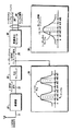
図1において、復調器10は、送信された信号5を受信する。なお、その送信された信号5の中に、搬送波周波数が、2−DPSKを用いて変調されている。典型的には、送信された信号5は、ブルートゥースのハイ・レート又は中間レート、標準準拠信号、又は802.11(b)準拠標準のような無線信号であろう。復調器10は、搬送波周波数を除去して、2−DPSKベースバンド信号15を生成する。当該2−DPSKベースバンド信号15は、複素値の信号であり、当該2−DPSKベースバンド信号15の実数部分は、同相信号(I)であり、当該信号の虚数部分は、直交信号(Q)と呼ばれる。
In FIG. 1, a
アナログ/ディジタル(A/D)サンプリング・モジュール20は、ディジタル・サンプル値の2つのシーケンスを、複素値のIQ信号15から生成する。ビュー26は、2つのシンボルの表示を有するサンプリングされた信号25を示す。2つのシンボルのそれぞれの中心が、示されている。1シンボル当たり4サンプルの図示されたサンプリング速度は、典型的なサンプリング速度であるが、しかし他のサンプリング速度を用いることもできる。
Analog / digital (A / D)
同期検出モジュール30は、サンプリングされた2−DPSKベースバンド信号25を用いて、パケット到着タイミング、又はパケットの開始を表すためシンボル中心サンプル・インデックス35及びサンプル間隔フラクション(Sample Interval Fraction)45値を発生する。より詳細には、シンボル中心サンプル・インデックス35及びサンプル間隔フラクション45は、パケットの中の特定のシンボル中心の位置、典型的には同期パターンの最初のシンボルを識別する。この検出されたタイミングを用いて、パケットの残りのフィールドのタイミングを導出する。シンボル中心サンプル・インデックス35は、同期パターン信号の一部分を表すビュー38を参照すると、シンボル中心の前のサンプルを示し、サンプルn+2は、インデックスされた又は識別されたサンプルである。サンプル間隔フラクション45は、シンボル中心サンプル・インデックス35からのシンボル中心の精細な時間推定を与える。サンプル間隔フラクション45の値は、サンプル周期の一部を表し、このサンプル周期の一部を用いて、特定のサンプルに対する唯1つのインデックスにより得られるタイミング解像度より良好なタイミング解像度を与える。
The
図2において、位相差分検出モジュール110は、複素値のサンプリングされた2−DPSKベースバンド信号25を用いて、位相差分サンプル115を生成する。なお、この位相差分サンプル115は、シンボル分離(symbol separation)を有する2つの信号値間の位相差を表す複素値である。シンボル分離は、重なっている部分を含まない1シンボル当たりのサンプルの数と理解される。例えば、1シンボルの間隔を有する2つの符号付きのサンプルは、ここで示されるように、ビュー26(図1)におけるサンプルn+1及びn+5であろう。
In FIG. 2, the phase
ビット相関モジュール120の内部で、ビット回復モジュール122が、位相差分サンプル115を用いて、候補ビット・ストリーム127を発生し、そしてバイナリ相関モジュール126は、候補ビット・ストリーム127を所定の同期ビット・パターン124と相関させて、ビット相関値125を生成する。所定の同期ビット・パターン124のそれらの値は、特定の同期パターンが生成するであろう単一ビット値の期待されたシーケンスを表す単一ビットのシーケンスである。ビット相関モジュール120の動作は、図3を参照してより詳細に説明される。
Within
信号相関モジュール130の内部で、サンプル相関モジュール132は、位相差分サンプル115を所定の同期シンボル・パターン134と相関させて、信号相関値135を生成する。シンボル中心での信号値が大きさにおいて等しいが、一方それらの極性が異なるので、所定の同期シンボル・パターン134は、そのシンボル中心での同期パターン信号の信号値を表すビットのシーケンスでもって表されることができる。それを行うことにより、相関演算における乗算及び加算/減算は、加算/減算のみに還元され、従ってコスト及びパワーを著しく低減する。一実施形態において、所定の同期シンボル・パターン134は、所定の同期ビット・パターン124と、それらが所定の同期ビット・パターン124と同じであることができる点で関連付けられる。信号相関値135は、4サンプル毎のサンプルを用いたサンプル・レートで相関値を表す。計算の効率を増すため、信号相関値135が、シンボルの中心にあると仮定された、1シンボル当たり唯1つのサンプルを用いて計算される。図4を参照する。この効率的なアプローチを用いて、所定の同期シンボル・パターン134は、+1又は−1により表されるシンボル値のシーケンスまで低減(還元)され、従って、乗算が、加算及び減算に還元される。
Within the
タイミング検出論理モジュール140内のデータ・パケット検出モジュール142は、ビット相関値125を用いて、ピーク到着インディケータを発生する。ピーク決定モジュール144は、このピーク到着インディケータ及び信号相関値135を用いて、シンボル中心サンプル・インデックス35及びサンプル間隔フラクション45を発生する。
The data
図3において、位相差分検出モジュール110が複素値のサンプリングされた2−DPSKベースバンド信号25から複素値の位相差分サンプル115を計算することが示される。信号25からの各複素サンプルx(n)が、1シンボル時間早く現れる複素サンプルの共役と乗算される。複素共役計算を用いて、2つのサンプルの位相差xd(n)を生成する。
In FIG. 3, it is shown that the phase
ビット回復モジュール122において、位相差分サンプル115の実数部が、ゼロのスレッショルドに対して比較されて、位相差分サンプル115から候補ビット・ストリーム127を発生し、そこにおいて、候補ビット・ストリーム127の各ビットは、+1又は−1のいずれかの値を有するよう取られる。位相差分サンプル115の虚数部は、この実施形態においては無視される。それは、所定の同期ビット・パターン124が、位相差がゼロ度のとき1で符号化され、そして位相差が180度のとき0で符号化されるからである。バイナリ相関モジュール126において、それぞれのビットが+1又は−1のいずれかの値であるK個のビット(S′1−S′K)を有する所定の同期ビット・パターン124は、上記サンプル・レートで、1ビット・シフト・レジスタに格納されている候補ビット・ストリーム127からのビットと相関されて、ビット相関値125を発生する。示された実施形態は、4サンプルのシンボル分離を有する。この相関の結果、即ち、各サンプル時間に対して1マルチビット・ディジタル値は、ビット相関値125を構成する。バイナリ相関モジュール126における相関が標準の信号相関で用いられるマルチビット・ディジタル値の非常にコストのかかる乗算より単一ビット値の単純な乗算を用いるので、高い効率が実現されることに注目されたい。
In the
図4は、信号相関モジュール130の特定の実現形態を示す。それぞれが+1又は−1の値を有するK個の単一ビット値(S* 1−S* K)を有する所定の同期シンボル・パターン134は、サンプル相関モジュール132により上記シンボル分離(4ビット毎)で位相差分サンプル115と相関される。この結果が、マルチビット値を格納する先入れ先出しレジスタ・スタックに格納される。この相関の結果、即ち、各サンプル時間に対して1マルチビット値は、信号相関値135を構成する。サンプル相関モジュール132に用いられるサンプルがシンボル分離にあるので、且つ所定の同期シンボル・パターン134が+1又は−1のシーケンスであるので、サンプル相関モジュール132における乗算は、加算及び減算に単純化されることに注目されたい。
FIG. 4 shows a specific implementation of the
図5は、タイミング検出論理モジュール140の特定の実施形態を示す。データ・パケット検出モジュール142のレジスタR2(4)及びR2(5)は、ビット相関値125の2つの連続値を連続的に格納する。R2(4)の中の値が(パケット・フォーマットに用いられる特定の同期パターンに適している)スレッショルドPより大きく、且つR2(5)の中の値がR2(4)の中の値より小さいとき、同期パターン又はパケットが検出され、そしてピーク到着インディケータがアサートされ、それがピーク決定モジュール144を活性化する。
FIG. 5 illustrates a specific embodiment of the timing
ピーク決定モジュール144は、5個の連続の信号相関値135を連続的に格納する。これらの値は、レジスタR1(1)乃至R1(5)に格納される。信号相関値R1(4)及びビット相関値R2(4)は、R1(5)及びR2(5)が対応するサンプル時間と同じサンプル時間に対応する。ピーク到着インディケータが設定されるとき、レジスタR1(1)乃至R1(5)の中の値は、ピーク到着インディケータの直前のシンボル時間にわたる信号相関値である。ピーク決定モジュール144におけるピーク同調アルゴリズムは、シンボル中心サンプル・インデックス35として、最大値を有するレジスタR1(1)乃至R1(5)を選択する。この最大値及びその隣接値を多項式推定で用いて、2次多項式曲線ピークを見つける。シンボル相関値と一致した非線形多項式に基づくこのピークは、真のピーク到着時間をより高い解像度で表す。シンボル中心サンプル・インデックス35は、真のピークの前のサンプル・インデックスであり、そしてサンプル間隔フラクション45は、シンボル中心サンプル・インデックス35から推定の真のピークまでのフラクショナルなサンプル間隔(fractional sample interval)を表す。
The
本出願における様々な機能及び構成要素は、データ・プロセッサ、又は複数の処理装置のような情報処理機械を用いて実行され得る。そのようなデータ・プロセッサは、マイクロプロセッサ、マイクロコントローラ、マイクロコンピュータ、ディジタル信号プロセッサ、状態機械、論理回路、及び/又は、ディジタル情報を操作命令に基づいて又は事前定義された要領で操作するいずれの装置であり得る。一般的に、ブロック図により表された様々な機能及びシステムは、本明細書にリストされた1又はそれより多い実現技術を用いて当業者により容易に実現される。命令を発行するデータ・プロセッサを用いるとき、その命令はメモリに格納される。そのようなメモリは、単一のメモリ装置又は複数のメモリ装置であり得る。そのようなメモリ装置は、読み出し専用メモリ・デバイス、ランダム・アクセス・メモリ・デバイス、磁気テープ・メモリ、フロッピィ・ディスク(登録商標)メモリ、ハード・ドライブ・メモリ、外部テープ、及び/又はディジタル情報を格納するいずれの装置であり得る。データ・プロセッサが、その機能のうちの1又はそれより多くの機能を状態機械又は論理回路を介して実行するとき、対応の命令を格納するメモリは、状態機械及び/又は論理回路を含む回路内に組み込まれ得るか、又はそれは、当該機能が組み合わせ論理を用いて実行されるので必要でない場合もあることに注目されたい。そのような情報処理機械は、コンピュータ、パーソナル・ディジタル・アシスタント(PDA)、ハンドヘルド計算装置、ケーブル・セットトップ・ボックス、インターネット・ケーブル・デバイス(例えば、セルラフォンのような)、及び類似のもののようなシステム、又はその一部であり得る。 The various functions and components in this application may be performed using an information processing machine such as a data processor or multiple processing units. Such a data processor may be a microprocessor, microcontroller, microcomputer, digital signal processor, state machine, logic circuit, and / or any one that manipulates digital information based on operational instructions or in a predefined manner. It can be a device. In general, the various functions and systems represented by the block diagrams are readily implemented by one of ordinary skill in the art using one or more implementation techniques listed herein. When using a data processor that issues instructions, the instructions are stored in memory. Such memory can be a single memory device or multiple memory devices. Such memory devices may include read only memory devices, random access memory devices, magnetic tape memory, floppy disk memory, hard drive memory, external tape, and / or digital information. It can be any device that stores. When a data processor performs one or more of its functions through a state machine or logic circuit, the memory that stores the corresponding instruction is in a circuit that includes the state machine and / or logic circuit. Note that it may or may not be necessary because the function is performed using combinatorial logic. Such information processing machines such as computers, personal digital assistants (PDAs), handheld computing devices, cable set-top boxes, Internet cable devices (such as cellular phones), and the like It can be a system or part thereof.
図面の前述の詳細な説明においては、その一部を形成し、また、開示を実行し得る例示的な特定の実施形態を示す添付図面に言及した。これらの実施形態は、当業者がこの開示を実行するのを可能にする程十分に詳細に説明され、そして他の実施形態を利用し得ること、及び論理的、機械的、化学的及び電気的変更がこの開示の趣旨又は範囲を逸脱することなしに行い得ることが理解される筈である。当業者がこの開示を実行するのを可能にするためには必要でない詳細を避けるため、この記載は、当業者に既知である或る一定の情報を省略している。更に、この開示の教示を取り入れる多くの他の変更された実施形態が、当業者により容易に構成され得る。従って、本発明は、本明細書に記載した特定の形式に限定する意図ではなく、反対に、特許請求の範囲に合理的に含まれることができるような代替、変更及び等価物をカバーすることを意図するものである。 In the foregoing detailed description of the drawings, reference has been made to the accompanying drawings that form a part hereof, and in which are shown by way of illustration specific embodiments in which the disclosure may be practiced. These embodiments are described in sufficient detail to enable those skilled in the art to practice this disclosure, and that other embodiments may be utilized, and logical, mechanical, chemical and electrical It should be understood that changes can be made without departing from the spirit or scope of this disclosure. To avoid details not necessary to enable those skilled in the art to practice this disclosure, this description omits certain information known to those skilled in the art. Moreover, many other modified embodiments that incorporate the teachings of this disclosure can be readily constructed by those skilled in the art. Accordingly, the present invention is not intended to be limited to the particular forms described herein, but on the contrary, covers alternatives, modifications and equivalents that may be reasonably included in the claims. Is intended.
Claims (5)
前記復調器の出力に結合された入力と、サンプリングされた差動位相偏移ベースバンド信号(25)を与えるための出力とを備えるアナログ/ディジタルサンプリング・モジュール(20)と、
前記復調器の出力に結合された入力と、受信されたシンボルの中心に対するサンプルの事前定義された関係を有する前記サンプリングされた差動位相偏移ベースバンド信号のサンプルを識別するシンボル中心サンプル・インデックス(35)を与えるための第1の出力と、前記シンボル中心サンプル・インデックスにより識別されたサンプルから前記受信されたシンボルの推定された中心までのサンプル周期のフラクショナルな部分を識別するサンプル間隔フラクション(45)を与えるための第2の出力とを備える同期検出モジュール(30)と
を備える差動位相偏移信号受信機。A demodulator (10) comprising a first input for receiving a differential phase shift signal (5) and an output for providing a differential phase shift baseband signal (15);
An analog / digital sampling module (20) comprising an input coupled to the output of the demodulator and an output for providing a sampled differential phase shifted baseband signal (25);
A symbol center sample index that identifies a sample of the sampled differential phase shifted baseband signal having a predefined relationship of samples to the center of the received symbol and an input coupled to the output of the demodulator A first output for providing (35) and a sample interval fraction that identifies a fractional portion of the sample period from the sample identified by the symbol center sample index to the estimated center of the received symbol ( 45) a differential phase shift signal receiver comprising a synchronization detection module (30) with a second output for providing.
前記のサンプリングされた差動位相偏移ベースバンド信号を受け取り、位相差分サンプル(115)のシーケンスを生成するための位相差分検出モジュール(110)と、
前記位相差分検出モジュールに応答する信号相関モジュール(130)と、を備え、
前記信号相関モジュールが、サンプル相関モジュール(132)を含み、
前記サンプル相関モジュール(132)が、位相差分サンプルのシーケンスを受け取るための第1の入力と、所定の同期シンボル・パターン(134)を受け取るための第2の入力とを有し、
前記所定の同期シンボル・パターンが、所定の同期ビット・パターンと関連付けられ、
前記サンプル相関モジュールが、シンボル相関値を生成し、
前記同期検出モジュールが更に、前記信号相関モジュールに応答して、シンボル中心サンプル・インデックス及びサンプル間隔フラクションを発生するタイミング検出モジュール(140)を備える
請求項1記載の差動位相偏移信号受信機。The synchronization detection module is
A phase difference detection module (110) for receiving the sampled differential phase shift baseband signal and generating a sequence of phase difference samples (115);
A signal correlation module (130) responsive to the phase difference detection module;
The signal correlation module includes a sample correlation module (132);
The sample correlation module (132) has a first input for receiving a sequence of phase difference samples and a second input for receiving a predetermined synchronization symbol pattern (134);
The predetermined synchronization symbol pattern is associated with a predetermined synchronization bit pattern;
The sample correlation module generates a symbol correlation value;
The differential phase shift signal receiver of claim 1, wherein the synchronization detection module further comprises a timing detection module (140) responsive to the signal correlation module to generate a symbol center sample index and a sample interval fraction.
差動位相偏移変調信号を受信して、位相差分サンプル(115)のシーケンスを生成するための位相差分検出モジュール(110)と、
前記位相差分検出モジュールに応答するビット相関モジュール(120)と、を備え、
前記ビット相関モジュールが、位相差分サンプルのシーケンスに応答して、回復された候補ビット・ストリーム(127)を生成するビット回復モジュール(122)を含み、
前記ビット相関モジュールが、バイナリ相関モジュール(126)を含み、
前記バイナリ相関モジュールが、前記の回復された候補ビット・ストリームを受け取るための第1の入力と、所定の同期ビット・パターン(124)を受け取るための第2の入力とを有し、
前記バイナリ相関モジュールが、ビット相関値(125)を生成し、
前記差動位相偏移信号受信機が更に、前記位相差分検出モジュールに応答する信号相関モジュール(130)を備え、
前記信号相関モジュールが、サンプル相関モジュール(132)を含み、
前記サンプル相関モジュールが、位相差分サンプルのシーケンスを受け取るための第1の入力と、所定の同期シンボル・パターン(134)を受け取るための第2の入力とを有し、
前記サンプル相関モジュールが、位相差分サンプルの選択されたサブセットについて相関を実行し、
前記信号相関モジュールが、信号相関値(135)を生成し、
前記差動位相偏移信号受信機が更に、前記ビット相関モジュールに応答し且つ前記信号相関モジュールに応答するタイミング検出論理モジュール(40)を備え、
前記タイミング検出論理モジュールが、同期インディケータをビット相関値及び信号相関値に基づいて発生する、差動位相偏移信号受信機。A differential phase shift signal receiver,
A phase difference detection module (110) for receiving a differential phase shift keyed signal and generating a sequence of phase difference samples (115);
A bit correlation module (120) responsive to the phase difference detection module;
The bit correlation module includes a bit recovery module (122) that generates a recovered candidate bit stream (127) in response to the sequence of phase difference samples;
The bit correlation module includes a binary correlation module (126);
The binary correlation module has a first input for receiving the recovered candidate bit stream and a second input for receiving a predetermined synchronization bit pattern (124);
The binary correlation module generates a bit correlation value (125);
The differential phase shift signal receiver further comprises a signal correlation module (130) responsive to the phase difference detection module;
The signal correlation module includes a sample correlation module (132);
The sample correlation module has a first input for receiving a sequence of phase difference samples and a second input for receiving a predetermined synchronization symbol pattern (134);
The sample correlation module performs correlation on a selected subset of phase difference samples;
The signal correlation module generates a signal correlation value (135);
The differential phase shift signal receiver further comprises a timing detection logic module (40) responsive to the bit correlation module and responsive to the signal correlation module;
A differential phase shift signal receiver, wherein the timing detection logic module generates a synchronization indicator based on a bit correlation value and a signal correlation value.
差動位相偏移変調信号(5)を受信するステップと、
前記差動位相偏移変調信号を復調して、ベースバンド差動位相偏移信号(15)を生成するステップと、
前記ベースバンド差動位相偏移信号から導出された位相差分サンプル(115)のシーケンスを決定するステップと、
前記位相差分サンプルのシーケンスから候補ビット・ストリーム(127)を回復するステップと、
前記候補ビット・ストリームを所定の同期ビット・パターンと相関させて、ビット・ストリーム相関値(125)を生成するステップと、
シンボル分離において前記位相差分サンプルのシーケンスを所定の同期シンボル・パターンと相関させて、信号相関値(135)を生成するステップと、
ビット・ストリーム相関値をスレッショルドと比較して、データ・パケットを検出するステップと、
前記の検出されたデータ・パケットのピーク同調を実行して、サンプル間隔フラクションを前記信号相関値に基づいて決定するステップと、
前記の検出されたデータ・パケットの開始時間に関する同期化タイミングを、前記の検出されたデータ・パケット及び前記サンプル間隔フラクションに基づいて決定するステップと
を備える方法。A method for synchronizing a received differential phase shift signal, comprising:
Receiving a differential phase shift keying signal (5);
Demodulating the differential phase shift keyed signal to generate a baseband differential phase shift signal (15);
Determining a sequence of phase difference samples (115) derived from the baseband differential phase shift signal;
Recovering a candidate bit stream (127) from the sequence of phase difference samples;
Correlating the candidate bit stream with a predetermined synchronization bit pattern to generate a bit stream correlation value (125);
Correlating the sequence of phase difference samples with a predetermined synchronization symbol pattern in symbol separation to generate a signal correlation value (135);
Comparing the bit stream correlation value with a threshold to detect a data packet;
Performing peak tuning of the detected data packet to determine a sample interval fraction based on the signal correlation value;
Determining a synchronization timing for a start time of the detected data packet based on the detected data packet and the sample interval fraction.
Applications Claiming Priority (2)
| Application Number | Priority Date | Filing Date | Title |
|---|---|---|---|
| US10/391,978 US6973142B2 (en) | 2003-03-19 | 2003-03-19 | Timing synchronization for M-DPSK channels |
| PCT/US2004/003095 WO2004095720A2 (en) | 2003-03-19 | 2004-02-04 | Timing synchronization for m-dpsk channels |
Publications (3)
| Publication Number | Publication Date |
|---|---|
| JP2006523420A JP2006523420A (en) | 2006-10-12 |
| JP2006523420A5 JP2006523420A5 (en) | 2007-03-22 |
| JP4383445B2 true JP4383445B2 (en) | 2009-12-16 |
Family
ID=32987804
Family Applications (1)
| Application Number | Title | Priority Date | Filing Date |
|---|---|---|---|
| JP2006508656A Expired - Fee Related JP4383445B2 (en) | 2003-03-19 | 2004-02-04 | Timing synchronization in M-DPSK channel |
Country Status (6)
| Country | Link |
|---|---|
| US (1) | US6973142B2 (en) |
| EP (1) | EP1606874A4 (en) |
| JP (1) | JP4383445B2 (en) |
| KR (1) | KR101067265B1 (en) |
| TW (1) | TWI335165B (en) |
| WO (1) | WO2004095720A2 (en) |
Cited By (5)
| Publication number | Priority date | Publication date | Assignee | Title |
|---|---|---|---|---|
| US9825791B2 (en) | 2015-12-30 | 2017-11-21 | Abov Semiconductor Co., Ltd. | Method and device for receiving frequency-shift keying signal |
| US9831902B2 (en) | 2015-12-30 | 2017-11-28 | Abov Semiconductor Co., Ltd. | Bluetooth smart signal receiving method and device using improved automatic gain control |
| US9912503B2 (en) | 2015-12-30 | 2018-03-06 | Abov Semiconductor Co., Ltd. | Bluetooth signal receiving method and device using improved carrier frequency offset compensation |
| US9954701B2 (en) | 2015-12-30 | 2018-04-24 | Abov Semiconductor Co., Ltd. | Bluetooth signal receiving method and device using improved packet detection and symbol timing acquisition |
| US10015029B2 (en) | 2015-12-30 | 2018-07-03 | Abov Semiconductor Co., Ltd. | Bluetooth signal receiving method and device using improved symbol timing offset compensation |
Families Citing this family (9)
| Publication number | Priority date | Publication date | Assignee | Title |
|---|---|---|---|---|
| KR20050062025A (en) * | 2003-12-19 | 2005-06-23 | 삼성전자주식회사 | Icmp packet generating system and method for multiple field errors of an ip packet |
| KR100867319B1 (en) * | 2005-08-08 | 2008-11-06 | 삼성전자주식회사 | Apparatus and method for detecting unsynchronized transmission in wireless communication system |
| US8098692B2 (en) * | 2006-08-29 | 2012-01-17 | Koninklijke Philips Electronics N.V. | Method and apparatus for high speed LVDS communication |
| KR100826248B1 (en) * | 2006-11-22 | 2008-04-29 | 삼성전자주식회사 | Demodulation method by detecting phase and apparatus thereof |
| KR101421406B1 (en) * | 2008-02-01 | 2014-07-23 | 성균관대학교산학협력단 | Correlation apparatus and method for frequency synchronization in broadband wireless access communicaion system |
| JP5214990B2 (en) * | 2008-02-06 | 2013-06-19 | ローム株式会社 | Differential phase shift keying (Differential Phase Shift Keying) signal demodulating circuit and radio equipment using the same |
| US9071470B2 (en) * | 2008-04-04 | 2015-06-30 | Maxlinear, Inc. | Low-complexity digital radio interface |
| US8488655B2 (en) * | 2009-04-14 | 2013-07-16 | Texas Instruments Incorporated | PHY layer parameters for body area network (BAN) devices |
| US10129014B2 (en) * | 2017-01-25 | 2018-11-13 | Samsung Electronics Co., Ltd. | System and method of performing initial timing synchronization of receivers of modulated signals |
Family Cites Families (11)
| Publication number | Priority date | Publication date | Assignee | Title |
|---|---|---|---|---|
| JPH06284159A (en) * | 1993-03-29 | 1994-10-07 | Toshiba Corp | Digital demodulator |
| US5854808A (en) * | 1993-09-14 | 1998-12-29 | Pacific Communication Sciences | Methods and apparatus for detecting the presence of a prescribed signal in a channel of a communications system |
| JP3414558B2 (en) * | 1995-08-25 | 2003-06-09 | 沖電気工業株式会社 | Maximum correlation value timing estimation circuit and receiving device |
| JP2850949B2 (en) * | 1995-12-15 | 1999-01-27 | 日本電気株式会社 | Digital PLL device |
| US5812207A (en) * | 1996-12-20 | 1998-09-22 | Intel Corporation | Method and apparatus for supporting variable oversampling ratios when decoding vertical blanking interval data |
| US6134286A (en) * | 1997-10-14 | 2000-10-17 | Ericsson Inc. | Synchronization techniques and systems for radiocommunication |
| US6587500B1 (en) * | 1999-12-17 | 2003-07-01 | Telefonaktiebolaget Lm Ericsson (Publ) | Symbol sampling time settlement of a hard decision radio receiver |
| US6643336B1 (en) | 2000-04-18 | 2003-11-04 | Widcomm, Inc. | DC offset and bit timing system and method for use with a wireless transceiver |
| US6424673B1 (en) | 2000-11-10 | 2002-07-23 | Motorola, Inc. | Method and apparatus in a wireless communication system for facilitating detection of, and synchronization with, a predetermined synchronization signal |
| US6738437B2 (en) * | 2001-03-15 | 2004-05-18 | Qualcomm Incorporated | Symbol recovery from an oversampled hard-decision binary stream |
| US7003056B2 (en) * | 2002-07-29 | 2006-02-21 | Freescale Semiconducter, Inc. | Symbol timing tracking and method therefor |
-
2003
- 2003-03-19 US US10/391,978 patent/US6973142B2/en not_active Expired - Lifetime
-
2004
- 2004-02-04 EP EP04708129A patent/EP1606874A4/en not_active Withdrawn
- 2004-02-04 JP JP2006508656A patent/JP4383445B2/en not_active Expired - Fee Related
- 2004-02-04 KR KR1020057017460A patent/KR101067265B1/en active IP Right Grant
- 2004-02-04 WO PCT/US2004/003095 patent/WO2004095720A2/en active Application Filing
- 2004-02-05 TW TW093102641A patent/TWI335165B/en not_active IP Right Cessation
Cited By (5)
| Publication number | Priority date | Publication date | Assignee | Title |
|---|---|---|---|---|
| US9825791B2 (en) | 2015-12-30 | 2017-11-21 | Abov Semiconductor Co., Ltd. | Method and device for receiving frequency-shift keying signal |
| US9831902B2 (en) | 2015-12-30 | 2017-11-28 | Abov Semiconductor Co., Ltd. | Bluetooth smart signal receiving method and device using improved automatic gain control |
| US9912503B2 (en) | 2015-12-30 | 2018-03-06 | Abov Semiconductor Co., Ltd. | Bluetooth signal receiving method and device using improved carrier frequency offset compensation |
| US9954701B2 (en) | 2015-12-30 | 2018-04-24 | Abov Semiconductor Co., Ltd. | Bluetooth signal receiving method and device using improved packet detection and symbol timing acquisition |
| US10015029B2 (en) | 2015-12-30 | 2018-07-03 | Abov Semiconductor Co., Ltd. | Bluetooth signal receiving method and device using improved symbol timing offset compensation |
Also Published As
| Publication number | Publication date |
|---|---|
| TW200428840A (en) | 2004-12-16 |
| US20040184564A1 (en) | 2004-09-23 |
| TWI335165B (en) | 2010-12-21 |
| EP1606874A2 (en) | 2005-12-21 |
| KR20050118285A (en) | 2005-12-16 |
| KR101067265B1 (en) | 2011-09-26 |
| US6973142B2 (en) | 2005-12-06 |
| WO2004095720A2 (en) | 2004-11-04 |
| WO2004095720A3 (en) | 2005-02-24 |
| JP2006523420A (en) | 2006-10-12 |
| EP1606874A4 (en) | 2008-06-04 |
Similar Documents
| Publication | Publication Date | Title |
|---|---|---|
| US5787123A (en) | Receiver for orthogonal frequency division multiplexed signals | |
| JP4383445B2 (en) | Timing synchronization in M-DPSK channel | |
| KR0136718B1 (en) | Synchronisation of ofdm signals | |
| US9991930B2 (en) | Configurable correlator for joint timing and frequency synchronization and demodulation | |
| WO2001028146A1 (en) | Apparatus for and method of adaptive synchronization in a spread spectrum communications receiver | |
| US7415078B2 (en) | Demodulation for phase modulation | |
| US20100215127A1 (en) | Method for estimating a carrier-frequency shift in a telecommunication signals receiver, notably a mobile device | |
| US8472569B2 (en) | Fine symbol timing estimation | |
| KR100359596B1 (en) | Signal communication system that can recognize reception of desired signal | |
| US9912511B2 (en) | Systems and methods for time synchronization between transmitters and receivers in a communication system | |
| JP5213580B2 (en) | Carrier offset detection circuit and detection method, and information communication device | |
| CN101115042A (en) | Transmitting apparatus and method, receiving apparatus and method | |
| JP2009010474A (en) | Signal processing section, and radio | |
| KR102097367B1 (en) | Independent packet detection method using orthogonal synchronization words and receiver thereof | |
| WO2008010283A1 (en) | Signal detecting apparatus | |
| JP4054032B2 (en) | Frame synchronization detection method | |
| JP3973332B2 (en) | Digital modulation / demodulation synchronization system | |
| CN114128154A (en) | Method for generating a signal comprising a time-sequential chirp, method for estimating a vehicle symbol using this signal, computer program product and corresponding devices | |
| JP5094469B2 (en) | Timing reproducing apparatus and receiving apparatus | |
| JP2007312347A (en) | Symbol timing detection apparatus and wireless terminal device | |
| JP2000151732A (en) | Carrier phase estimation device and demodulator using the estimation device | |
| JP3688260B2 (en) | Carrier frequency synchronization method and carrier frequency synchronization circuit for OFDM signal demodulator | |
| JP4803079B2 (en) | Demodulator | |
| JP2000151545A (en) | Demodulator, demodulation method and provision medium | |
| JP4847373B2 (en) | Frame synchronization detection method |
Legal Events
| Date | Code | Title | Description |
|---|---|---|---|
| A521 | Request for written amendment filed |
Free format text: JAPANESE INTERMEDIATE CODE: A523 Effective date: 20070202 |
|
| A621 | Written request for application examination |
Free format text: JAPANESE INTERMEDIATE CODE: A621 Effective date: 20070202 |
|
| A977 | Report on retrieval |
Free format text: JAPANESE INTERMEDIATE CODE: A971007 Effective date: 20090819 |
|
| TRDD | Decision of grant or rejection written | ||
| A01 | Written decision to grant a patent or to grant a registration (utility model) |
Free format text: JAPANESE INTERMEDIATE CODE: A01 Effective date: 20090825 |
|
| A01 | Written decision to grant a patent or to grant a registration (utility model) |
Free format text: JAPANESE INTERMEDIATE CODE: A01 |
|
| A61 | First payment of annual fees (during grant procedure) |
Free format text: JAPANESE INTERMEDIATE CODE: A61 Effective date: 20090918 |
|
| FPAY | Renewal fee payment (event date is renewal date of database) |
Free format text: PAYMENT UNTIL: 20121002 Year of fee payment: 3 |
|
| R150 | Certificate of patent or registration of utility model |
Ref document number: 4383445 Country of ref document: JP Free format text: JAPANESE INTERMEDIATE CODE: R150 Free format text: JAPANESE INTERMEDIATE CODE: R150 |
|
| FPAY | Renewal fee payment (event date is renewal date of database) |
Free format text: PAYMENT UNTIL: 20131002 Year of fee payment: 4 |
|
| R250 | Receipt of annual fees |
Free format text: JAPANESE INTERMEDIATE CODE: R250 |
|
| R250 | Receipt of annual fees |
Free format text: JAPANESE INTERMEDIATE CODE: R250 |
|
| R250 | Receipt of annual fees |
Free format text: JAPANESE INTERMEDIATE CODE: R250 |
|
| S111 | Request for change of ownership or part of ownership |
Free format text: JAPANESE INTERMEDIATE CODE: R313113 |
|
| R350 | Written notification of registration of transfer |
Free format text: JAPANESE INTERMEDIATE CODE: R350 |
|
| R250 | Receipt of annual fees |
Free format text: JAPANESE INTERMEDIATE CODE: R250 |
|
| R250 | Receipt of annual fees |
Free format text: JAPANESE INTERMEDIATE CODE: R250 |
|
| R250 | Receipt of annual fees |
Free format text: JAPANESE INTERMEDIATE CODE: R250 |
|
| R250 | Receipt of annual fees |
Free format text: JAPANESE INTERMEDIATE CODE: R250 |
|
| R250 | Receipt of annual fees |
Free format text: JAPANESE INTERMEDIATE CODE: R250 |
|
| R250 | Receipt of annual fees |
Free format text: JAPANESE INTERMEDIATE CODE: R250 |
|
| LAPS | Cancellation because of no payment of annual fees |