JP4374463B2 - Oscillation frequency control circuit - Google Patents
Oscillation frequency control circuit Download PDFInfo
- Publication number
- JP4374463B2 JP4374463B2 JP2006349519A JP2006349519A JP4374463B2 JP 4374463 B2 JP4374463 B2 JP 4374463B2 JP 2006349519 A JP2006349519 A JP 2006349519A JP 2006349519 A JP2006349519 A JP 2006349519A JP 4374463 B2 JP4374463 B2 JP 4374463B2
- Authority
- JP
- Japan
- Prior art keywords
- voltage
- control
- information
- circuit
- reference signal
- Prior art date
- Legal status (The legal status is an assumption and is not a legal conclusion. Google has not performed a legal analysis and makes no representation as to the accuracy of the status listed.)
- Active
Links
Images


Classifications
-
- H—ELECTRICITY
- H03—ELECTRONIC CIRCUITRY
- H03L—AUTOMATIC CONTROL, STARTING, SYNCHRONISATION, OR STABILISATION OF GENERATORS OF ELECTRONIC OSCILLATIONS OR PULSES
- H03L7/00—Automatic control of frequency or phase; Synchronisation
- H03L7/06—Automatic control of frequency or phase; Synchronisation using a reference signal applied to a frequency- or phase-locked loop
- H03L7/08—Details of the phase-locked loop
- H03L7/14—Details of the phase-locked loop for assuring constant frequency when supply or correction voltages fail or are interrupted
-
- H—ELECTRICITY
- H03—ELECTRONIC CIRCUITRY
- H03L—AUTOMATIC CONTROL, STARTING, SYNCHRONISATION, OR STABILISATION OF GENERATORS OF ELECTRONIC OSCILLATIONS OR PULSES
- H03L7/00—Automatic control of frequency or phase; Synchronisation
- H03L7/06—Automatic control of frequency or phase; Synchronisation using a reference signal applied to a frequency- or phase-locked loop
- H03L7/08—Details of the phase-locked loop
- H03L7/085—Details of the phase-locked loop concerning mainly the frequency- or phase-detection arrangement including the filtering or amplification of its output signal
- H03L7/095—Details of the phase-locked loop concerning mainly the frequency- or phase-detection arrangement including the filtering or amplification of its output signal using a lock detector
-
- H—ELECTRICITY
- H03—ELECTRONIC CIRCUITRY
- H03L—AUTOMATIC CONTROL, STARTING, SYNCHRONISATION, OR STABILISATION OF GENERATORS OF ELECTRONIC OSCILLATIONS OR PULSES
- H03L7/00—Automatic control of frequency or phase; Synchronisation
- H03L7/06—Automatic control of frequency or phase; Synchronisation using a reference signal applied to a frequency- or phase-locked loop
- H03L7/08—Details of the phase-locked loop
- H03L7/085—Details of the phase-locked loop concerning mainly the frequency- or phase-detection arrangement including the filtering or amplification of its output signal
- H03L7/093—Details of the phase-locked loop concerning mainly the frequency- or phase-detection arrangement including the filtering or amplification of its output signal using special filtering or amplification characteristics in the loop
-
- H—ELECTRICITY
- H03—ELECTRONIC CIRCUITRY
- H03L—AUTOMATIC CONTROL, STARTING, SYNCHRONISATION, OR STABILISATION OF GENERATORS OF ELECTRONIC OSCILLATIONS OR PULSES
- H03L7/00—Automatic control of frequency or phase; Synchronisation
- H03L7/06—Automatic control of frequency or phase; Synchronisation using a reference signal applied to a frequency- or phase-locked loop
- H03L7/08—Details of the phase-locked loop
- H03L7/14—Details of the phase-locked loop for assuring constant frequency when supply or correction voltages fail or are interrupted
- H03L7/146—Details of the phase-locked loop for assuring constant frequency when supply or correction voltages fail or are interrupted by using digital means for generating the oscillator control signal
Description
本発明は、発振器の発振周波数制御回路に係り、特に、出力信号に同期させ、自己の周波数を補正し、高安定な基準信号がないときでも一定期間安定に保つことができる発振周波数制御回路に関する。 The present invention relates to an oscillation frequency control circuit of an oscillator, and more particularly to an oscillation frequency control circuit that can be synchronized with an output signal, correct its own frequency, and can be kept stable for a certain period even when there is no highly stable reference signal. .
次世代移動体通信及び地上デジタル放送などの基地局では、周波数基準信号に対する要求精度は益々高まっている。
周波数基準信号として、セシウム周波数基準発振器、ルビシウム周波数基準発振器、GPS信号による周波数同期型の基準発振器などが、放送、通信分野のシステムで利用されている。
In base stations such as next-generation mobile communication and digital terrestrial broadcasting, the required accuracy for frequency reference signals is increasing.
As a frequency reference signal, a cesium frequency reference oscillator, a rubidium frequency reference oscillator, a frequency-synchronized reference oscillator using a GPS signal, and the like are used in systems in the broadcasting and communication fields.
しかしながら、これらの発振器は、一般的に高価であるため、それら発振器からの基準信号は分配して装置の基準信号源として使用される。 However, since these oscillators are generally expensive, the reference signals from these oscillators are distributed and used as a reference signal source for the device.
分配された基準信号は、通信システムの基準クロックに使用される。
具体的には、PLL(Phase Locked Loop)回路の位相比較のリファレンス信号、DSP(Digital Signal Processor)、FPGA(Field Programmable Gate Array)などの基準クロック信号、DA(Digital/Analog)コンバータ、AD(Analog/Digital)コンバータのサンプリングクロックとして使用される。
The distributed reference signal is used as a reference clock for the communication system.
Specifically, reference signal for phase comparison of PLL (Phase Locked Loop) circuit, reference clock signal such as DSP (Digital Signal Processor), FPGA (Field Programmable Gate Array), DA (Digital / Analog) converter, AD (Analog) / Digital) Used as a sampling clock for the converter.
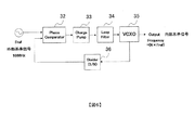
[従来のPLL回路:図6]
次に、従来のPLL回路について図6を参照しながら説明する。図6は、一般的PLL回路の構成ブロック図である。
PLL回路は、図6に示すように、外部基準信号(Fref )と1/N分周された信号を比較し、位相差信号を出力する位相比較器(Phase Comparator)32と、位相差をパルス幅の電圧で出力するチャージポンプ(Charge Pump)33と、チャージポンプ33からの出力電圧を平滑化するループフィルタ(Loop Filter)34と、ループフィルタ34からの制御電圧によって周波数を変更して希望する周波数(内部基準信号:Output Frequency)を発振出力する電圧制御機能付き水晶発振器(VCXO:Voltage Controlled Crystal Oscillator)35と、VCXO35の出力(内部基準信号)を1/Nに分周する分周器(Divider)36とを備えている。
尚、内部基準信号は、N×Fref の信号である。
[Conventional PLL circuit: FIG. 6]
Next, a conventional PLL circuit will be described with reference to FIG. FIG. 6 is a configuration block diagram of a general PLL circuit.
As shown in FIG. 6, the PLL circuit compares an external reference signal (Fref) with a signal divided by 1 / N, and outputs a phase difference signal (Phase Comparator) 32 and pulses the phase difference. A
The internal reference signal is an N × Fref signal.
PLL回路は、外部より入力された基準信号と内部のVCXO35の位相差が一定になるよう、内部のVCXO35に対してフィードバック制御をかけることで、基準信号に同期した発振器出力を得るものである。
The PLL circuit obtains an oscillator output synchronized with the reference signal by applying feedback control to the
具体的には、位相比較器32は、高安定な外部基準信号と、入力電圧により周波数制御するVCXO35からの出力信号との位相を比較し、位相比較結果を平滑化した直流電圧がVCXO35にフィードバックされるPLL制御を行うことで、高精度の信号生成を行うものである。
PLL回路は、通信、放送装置などにおいて広く使用されている。
Specifically, the
The PLL circuit is widely used in communication and broadcasting apparatuses.
尚、従来の発振器における発振周波数制御回路に関する先行技術として、特開2000−083003号公報(特許文献1)、特開2003−179489号公報(特許文献2)がある。 As prior arts related to an oscillation frequency control circuit in a conventional oscillator, there are JP-A-2000-083003 (Patent Document 1) and JP-A-2003-179489 (Patent Document 2).
特許文献1には、周波数カウンタがパルス幅に対応する時間内に入力されるVCO(Voltage Controlled Oscillator)の出力信号に同期した計数動作を行っており、VCOの発振周波数に対応した計数値がラッチ回路に保持され、CPUは係数値が所定範囲内から外れている場合には、VCOの印加電圧を変化させてフリーラン周波数が所定範囲になるよう調整するフレーラン周波数調整方式が記載されている。
In
また、特許文献2には、マイクロコンピュータが、位相比較器の出力が所定レベルにある期間中にVCOの出力パルス信号のパルスをカウントし、そのカウント値に応じて制御用のデータを更新し、そのデータをDAC(Digital Analog Converter)でアナログ信号としてLPF(Low Pass Filter)からの信号と結合させてVCOの周波数制御信号とする電圧制御発振器の自走周波数の自動調整機能を有する位相ロックループ回路が記載されている。
Further, in
しかしながら、上記従来のPLL回路では、基準信号の入力がなくなったときは、位相比較ができなくなるため、他の外部基準信号への切り替えを行うか、または電圧制御発振器のフリーラン(自走)で動作することになるが、予備系の他の外部基準信号への切り替え時は、再びPLL制御が行われるので、基準信号の偏差が外部基準信号に依存するので問題とならないが、自走したときには切り替え時の位相比較結果により周波数が過剰に制御され、上限又は下限の周波数に張り付いて周波数ズレが大きくなるという問題点があった。 However, in the above conventional PLL circuit, when no reference signal is input, phase comparison cannot be performed. Therefore, switching to another external reference signal is performed, or the voltage controlled oscillator is free-runned (self-running). Although it will operate, when switching to another external reference signal in the standby system, PLL control is performed again, so there is no problem because the deviation of the reference signal depends on the external reference signal, but when self-running There is a problem in that the frequency is excessively controlled by the phase comparison result at the time of switching, and the frequency shift increases due to sticking to the upper limit or lower limit frequency.
自走した時でも、短期的な問題解決として、電圧制御発振器として温度補償型の高安定な水晶発振器(VC−TCXO)が使われることがある。
しかしながら、この場合、例えば、±0.5ppmの周波数安定度で動作するが、経年変化があるため、長期間性能を満足させることはできないものである。
Even when self-running, as a short-term problem-solving, a temperature-compensated highly stable crystal oscillator (VC-TCXO) may be used as a voltage-controlled oscillator.
However, in this case, for example, although it operates with a frequency stability of ± 0.5 ppm, the performance cannot be satisfied for a long time due to aging.
例えば、エージング特性として年±1ppm程度の変動があると仮定すると、10年経過すると最大で10.5ppmの周波数偏差が発生する。これは、通信している搬送波出力周波数が800MHzとすると、基準周波数の周波数偏差と同様に、8.4kHzの周波数ズレが発生する。このような周波数偏差はシステムとして許容できない。 For example, assuming that there is a fluctuation of about ± 1 ppm per year as the aging characteristic, a frequency deviation of 10.5 ppm at maximum occurs after 10 years. If the carrier wave output frequency in communication is 800 MHz, a frequency deviation of 8.4 kHz occurs as in the case of the frequency deviation of the reference frequency. Such a frequency deviation is unacceptable as a system.
また、電圧制御機能付き恒温槽水晶発振器(VC−OCXO)が使用される高安定なシステムの場合でも、エージング特性として長期間では周波数偏差が発生するため、一定期間毎に校正作業が発生し、校正作業が面倒であるとの問題点があった。 In addition, even in the case of a highly stable system in which a constant-temperature bath crystal oscillator with a voltage control function (VC-OCXO) is used, frequency deviation occurs over a long period of time as aging characteristics, so calibration work occurs every fixed period, There was a problem that the calibration work was troublesome.
また、特許文献1,2では、VCOの出力をカウントして、若しくは位相比較器の出力をカウントして自走周波数の調整を行うものであるが、外部基準信号の異常を直接検出して周波数調整を行うものではなく、更に経年変化に十分対応できるものとはなっていなかった。
In
[VCXOの制御電圧特性:図7]
尚、VCXOの制御電圧特性を図7に示す。図7は、電圧制御機能付き水晶発振器の制御電圧特性例を示す図である。図7において、横軸は制御電圧であり、縦軸は周波数偏差である。
図7の例のVCXOでは、制御電圧が0〜4Vであれば、動作可能であるが、4V以上では動作不能となる。
VCXOの場合でも、時間の経過に伴って、周波数偏差が上昇するため、適正な制御電圧が変化するものである。
[Control voltage characteristics of VCXO: FIG. 7]
The control voltage characteristics of VCXO are shown in FIG. FIG. 7 is a diagram illustrating an example of control voltage characteristics of a crystal oscillator with a voltage control function. In FIG. 7, the horizontal axis represents the control voltage, and the vertical axis represents the frequency deviation.
The VCXO in the example of FIG. 7 can operate when the control voltage is 0 to 4V, but cannot operate when the control voltage is 4V or higher.
Even in the case of VCXO, the frequency deviation increases with the passage of time, so that an appropriate control voltage changes.
本発明は上記実情に鑑みて為されたもので、自己の周波数を補正し、高安定な基準信号の入力がなく、自走したときでも発振周波数を安定に保つことができる発振周波数制御回路を提供することを目的とする。 The present invention has been made in view of the above circumstances, and an oscillation frequency control circuit that corrects its own frequency, does not have a highly stable reference signal input, and can keep the oscillation frequency stable even when it is self-running. The purpose is to provide.
上記従来例の問題点を解決するための本発明は、発振周波数制御回路において、電圧制御発振器と、前記電圧制御発振器からの出力を分周する分周器と、外部基準信号と分周器からの出力の位相を比較し、位相差信号を出力する位相比較器と、位相比較器からの出力を平滑化して電圧制御発振器に制御電圧を出力するループフィルタと、ループフィルタからの出力について電圧レベルを検出して最新の制御電圧情報を出力するレベル検出回路と、外部基準信号を検波する検波回路と、パルス生成の情報が入力されるとパルスを生成してループフィルタに出力するパルス生成回路と、電圧制御発振器に出力される制御電圧の値を制御電圧情報として、複数の制御電圧情報とそれに対応するパルス生成の情報を記憶する電圧・パルス生成の情報テーブルを記憶し、レベル検出回路で検出された電圧レベルを最新の制御電圧情報として記憶するメモリと、位相比較器とループフィルタとの接続をオン/オフするスイッチと、レベル検出回路で検出された電圧レベルを入力し、当該電圧レベルを最新の制御電圧情報としてメモリに記憶されている最新の制御電圧情報を更新すると共に、検波回路で検出された外部基準信号のレベルが適正範囲内であればスイッチをオンとし、レベルが適正範囲外であればスイッチをオフとしてメモリに記憶された更新された最新の制御電圧情報を読み取り、当該最新の制御電圧情報に対応するパルス生成の情報を電圧・パルス生成の情報テーブルから読み取り、当該パルス生成の情報をパルス生成回路に出力する制御部とを有し、パルス生成回路は、パルス幅変調回路であり、制御部から出力されるパルス生成の情報は、パルス幅変調デューティーサイクルの情報であることを特徴とする。 The present invention for solving the problems of the above-described conventional example includes, in an oscillation frequency control circuit, a voltage controlled oscillator, a frequency divider for dividing the output from the voltage controlled oscillator, an external reference signal, and a frequency divider. A phase comparator that outputs a phase difference signal, a loop filter that smoothes the output from the phase comparator and outputs a control voltage to a voltage controlled oscillator, and a voltage level for the output from the loop filter A level detection circuit that detects the current and outputs the latest control voltage information, a detection circuit that detects an external reference signal, a pulse generation circuit that generates a pulse and outputs it to a loop filter when pulse generation information is input, , as the control voltage information the value of the control voltage output to the voltage controlled oscillator, the voltage pulse generation information te for storing information of a pulse generator and the corresponding plurality of control voltage information Stores table, a memory for storing a voltage level detected by the level detection circuit as the latest control voltage information, a switch for turning on / off the connection between the phase comparator and the loop filter, which is detected by the level detection circuit Input the voltage level, update the latest control voltage information stored in the memory as the latest control voltage information , and if the level of the external reference signal detected by the detection circuit is within the appropriate range If the switch is turned on and the level is out of the proper range, the switch is turned off, the latest updated control voltage information stored in the memory is read, and the pulse generation information corresponding to the latest control voltage information is read as voltage / pulse. reading from the generation of information table, and a control unit for outputting information of the pulse generator to the pulse generating circuit, pulse generating circuit, pulse A modulation circuit, a pulse generation information output from the control unit is characterized in that the information of the pulse width modulation duty cycle.
本発明は、上記発振周波数制御回路において、メモリに記憶された制御電圧情報を、電圧制御発振器を制御可能な制御電圧において中心制御電圧の値としたことを特徴とする。 The present invention is characterized in that, in the oscillation frequency control circuit, the control voltage information stored in the memory is a value of a central control voltage in a control voltage capable of controlling the voltage controlled oscillator.
本発明は、上記発振周波数制御回路において、メモリには、経年変化の時間に対する適正な制御電圧情報とそれに対応するパルス生成の情報を記憶する経年変化特性テーブルを記憶し、制御部は、内部にタイマーを備えて時間を計測し、外部基準信号のレベルが適正範囲外であるときに、メモリの経年変化特性テーブルから計測した時間に応じた制御電圧情報を検索し、検索した制御電圧情報に対応するパルス生成の情報を読み取り、パルス生成回路に出力することを特徴とする。 The present invention is the oscillation frequency control circuit, the memory stores the aging characteristics table storing proper control voltage information and the pulse generation information corresponding thereto with respect to time warp the year changes, the control unit, the internal The timer is equipped with a timer to measure the time, and when the level of the external reference signal is outside the appropriate range, the control voltage information corresponding to the measured time is retrieved from the aging characteristics table of the memory, and the retrieved control voltage information The corresponding pulse generation information is read and output to the pulse generation circuit.
本発明は、上記発振周波数制御回路において、電圧制御発振器の代わりに、電圧制御機能付き水晶発振器、温度補償型の水晶発振器又は電圧制御機能付き恒温槽水晶発振器を用いたことを特徴とする。 The present invention is characterized in that, in the oscillation frequency control circuit, a crystal oscillator with a voltage control function, a temperature compensation type crystal oscillator, or a thermostat crystal oscillator with a voltage control function is used instead of the voltage control oscillator.
本発明は、上記発振周波数制御回路を用いた校正方法において、外部基準信号が入力される端子から外部基準信号を入力させない状態とし、周波数偏差が上昇又は下降するタイミングで前記端子から外部基準信号を入力し、その後、外部基準信号の入力を停止することで、制御部が、中心制御電圧の値に従って自走制御し、周波数偏差が中心周波数に戻ってきて校正が為されることを特徴とする。 The present invention provides a calibration method using the oscillation frequency control circuit, a state which does not enter the external reference signal from a terminal to which the external reference signal is input, the external reference signal from the terminal at a timing when the frequency shift increases or decreases After inputting, the input of the external reference signal is stopped, so that the control unit performs free-running control according to the value of the center control voltage, and the frequency deviation returns to the center frequency and calibration is performed. .
本発明は、上記発振周波数制御回路を用いた校正方法において、外部基準信号が入力される端子から外部基準信号を入力させない状態とし、周波数偏差が上昇するタイミングで前記端子から外部基準信号を入力し、その後、外部基準信号の入力を停止することで、制御部が、経年変化特性テーブルを参照し、計測した時間に応じた制御電圧の値に従って自走制御し、周波数偏差が中心周波数に戻ってきて校正が為されることを特徴とする。 The present invention provides a calibration method using the oscillation frequency control circuit, a state which does not enter the external reference signal from a terminal to which the external reference signal is input, inputting an external reference signal from the terminal at a timing when the frequency deviation is increased After that, by stopping the input of the external reference signal, the control unit refers to the aging characteristic table and performs self-running control according to the value of the control voltage corresponding to the measured time, and the frequency deviation returns to the center frequency. It is characterized by being calibrated.
本発明によれば、電圧制御発振器と、前記電圧制御発振器からの出力を分周する分周器と、外部基準信号と分周器からの出力の位相を比較し、位相差信号を出力する位相比較器と、位相比較器からの出力を平滑化して電圧制御発振器に制御電圧を出力するループフィルタと、ループフィルタからの出力について電圧レベルを検出して最新の制御電圧情報を出力するレベル検出回路と、外部基準信号を検波する検波回路と、パルス生成の情報が入力されるとパルスを生成してループフィルタに出力するパルス生成回路と、電圧制御発振器に出力される制御電圧の値を制御電圧情報として、複数の制御電圧情報とそれに対応するパルス生成の情報を記憶する電圧・パルス生成の情報テーブルを記憶し、レベル検出回路で検出された電圧レベルを最新の制御電圧情報として記憶するメモリと、位相比較器とループフィルタとの接続をオン/オフするスイッチと、レベル検出回路で検出された電圧レベルを入力し、当該電圧レベルを最新の制御電圧情報としてメモリに記憶されている最新の制御電圧情報を更新すると共に、検波回路で検出された外部基準信号のレベルが適正範囲内であればスイッチをオンとし、レベルが適正範囲外であればスイッチをオフとしてメモリに記憶された更新された最新の制御電圧情報を読み取り、当該最新の制御電圧情報に対応するパルス生成の情報を電圧・パルス生成の情報テーブルから読み取り、当該パルス生成の情報をパルス生成回路に出力する制御部とを有し、パルス生成回路は、パルス幅変調回路であり、制御部から出力されるパルス生成の情報は、パルス幅変調デューティーサイクルの情報である、発振周波数制御回路としているので、自己の周波数を補正し、高安定な基準信号の入力がなく、自走したときでも発振周波数を安定に保つことができる効果がある。 According to the present invention, the voltage-controlled oscillator, the frequency divider that divides the output from the voltage-controlled oscillator, and the phase that outputs the phase difference signal by comparing the phase of the output from the external reference signal and the frequency divider A comparator, a loop filter that smoothes the output from the phase comparator and outputs a control voltage to the voltage controlled oscillator, and a level detection circuit that detects the voltage level of the output from the loop filter and outputs the latest control voltage information When a detector circuit for detecting an external reference signal, and a pulse generation circuit which outputs to the loop filter when the pulse generation information is input to generate a pulse, controls the value of the control voltage output to the voltage controlled oscillator voltage as the information, it stores the information table of the voltage pulse generator for storing the pulse generation information corresponding thereto and a plurality of control voltage information, the voltage level detected by the level detection circuit outermost A memory for storing a control voltage information, a switch for turning on / off the connection between the phase comparator and the loop filter, enter the voltage level detected by the level detection circuit, the voltage level as the latest control voltage information Updates the latest control voltage information stored in the memory and turns on the switch if the level of the external reference signal detected by the detection circuit is within the proper range, and turns off the switch if the level is outside the proper range The latest updated control voltage information stored in the memory is read, the pulse generation information corresponding to the latest control voltage information is read from the voltage / pulse generation information table, and the pulse generation information is read from the pulse generation circuit. The pulse generation circuit is a pulse width modulation circuit, and the pulse generation information output from the control unit is Pulse width Ru information der modulation duty cycle, since the oscillation frequency control circuit corrects the frequency of the self, no input of highly stable reference signal, to keep the oscillation frequency stably even when the self-propelled There is an effect.
本発明によれば、上記発振周波数制御回路において、メモリに記憶された制御電圧情報を、電圧制御発振器を制御可能な制御電圧において中心制御電圧の値とした上記周波数発振回路としているので、自己の周波数を補正し、発振周波数を安定に保つことができる効果がある。 According to the present invention, in the oscillation frequency control circuit, the control voltage information stored in the memory is the frequency oscillation circuit having the value of the center control voltage in the control voltage that can control the voltage controlled oscillator. There is an effect that the frequency can be corrected and the oscillation frequency can be kept stable.
本発明によれば、メモリには、経年変化の時間に対する適正な制御電圧情報とそれに対応するパルス生成の情報を記憶する経年変化特性テーブルを記憶し、制御部は、内部にタイマーを備えて時間を計測し、外部基準信号のレベルが適正範囲外であるときに、メモリの経年変化特性テーブルから計測した時間に応じた制御電圧情報を検索し、検索した制御電圧情報に対応するパルス生成の情報を読み取り、パルス生成回路に出力する上記発振周波数制御回路としているので、周波数補正を経年変化に対応させることができる効果がある。 According to the present invention, the memory stores the aging characteristics table storing proper control voltage information and the pulse generation information corresponding thereto with respect to time warp the year changes, the control unit includes a timer inside When the time is measured and the level of the external reference signal is outside the appropriate range, control voltage information corresponding to the measured time is retrieved from the aging characteristics table of the memory, and pulse generation corresponding to the retrieved control voltage information is performed. Since the oscillation frequency control circuit that reads information and outputs it to the pulse generation circuit is used, there is an effect that frequency correction can be made to cope with aging.
本発明によれば、外部基準信号が入力される端子から外部基準信号を入力させない状態とし、周波数偏差が上昇又は下降するタイミングで前記端子から外部基準信号を入力し、その後、外部基準信号の入力を停止することで、制御部が、中心制御電圧の値に従って自走制御し、周波数偏差が中心周波数に戻ってきて校正が為される上記発振周波数制御回路を用いた校正方法としているので、特別の装置を用いなくても校正できる効果がある。 According to the present invention, a state that does not enter the external reference signal from a terminal to which the external reference signal is input, inputting an external reference signal from the terminal at a timing when the frequency deviation rises or falls, then the input of the external reference signal Since the control unit performs the self-running control according to the value of the center control voltage, and the calibration method using the oscillation frequency control circuit in which the frequency deviation returns to the center frequency and is calibrated, it is special. There is an effect that can be calibrated without using the device.
本発明によれば、外部基準信号が入力される端子から外部基準信号を入力させない状態とし、周波数偏差が上昇するタイミングで前記端子から外部基準信号を入力し、その後、外部基準信号の入力を停止することで、制御部が、経年変化特性テーブルを参照し、計測した時間に応じた制御電圧の値に従って自走制御し、周波数偏差が中心周波数に戻ってきて校正が為される上記発振周波数制御回路を用いた校正方法としているので、特別の装置を用いることなく、経年変化に対応した校正ができる効果がある。 According to the present invention, a state that does not enter the external reference signal from a terminal to which the external reference signal is input, inputting an external reference signal from the terminal at a timing when the frequency deviation is increased, then stopped the input of the external reference signal By doing so, the control unit refers to the aging characteristic table, performs self-running control according to the value of the control voltage according to the measured time, and the oscillation frequency control in which the frequency deviation returns to the center frequency and the calibration is performed. Since the calibration method uses a circuit, there is an effect that calibration corresponding to aging can be performed without using a special device.
[実施の形態の概要]
本発明の実施の形態について図面を参照しながら説明する。
本発明の実施の形態に係る発振周波数制御回路は、電圧制御発振器と、電圧制御発振器からの出力を分周する分周器と、外部基準信号と分周器からの出力の位相を比較し、位相差信号を出力する位相比較器と、位相比較器からの出力を平滑化して出力するループフィルタと、外部基準信号を検波する検波回路と、パルス生成の情報が入力されるとパルスを生成してループフィルタに出力するパルス生成回路と、規定の電圧情報とそれに対応するパルス生成の情報を記憶するメモリと、位相比較器とループフィルタとの接続をオン/オフするスイッチと、検波回路で検出された外部基準信号のレベルが適正範囲内であればスイッチをオンとし、レベルが適正範囲外であればスイッチをオフとしてメモリに記憶されたパルス生成の情報をパルス発生回路に出力する制御部とを有するものであり、自己の周波数を補正し、高安定な基準信号の入力がなく、自走したときでも発振周波数を安定に保つことができるものである。
[Outline of the embodiment]
Embodiments of the present invention will be described with reference to the drawings.
The oscillation frequency control circuit according to the embodiment of the present invention compares the phase of the output from the voltage controlled oscillator, the frequency divider that divides the output from the voltage controlled oscillator, the external reference signal and the frequency divider, A phase comparator that outputs a phase difference signal, a loop filter that smoothes and outputs the output from the phase comparator, a detection circuit that detects an external reference signal, and a pulse when information on pulse generation is input Detecting with a pulse generation circuit that outputs to the loop filter, a memory that stores the specified voltage information and the corresponding pulse generation information, a switch that turns on / off the connection between the phase comparator and the loop filter, and a detection circuit If the level of the external reference signal is within the proper range, the switch is turned on, and if the level is outside the proper range, the switch is turned off and the pulse generation information stored in the memory is generated. Those having a control unit for outputting to the circuit, and corrects the frequency of the self, no input of highly stable reference signal, in which even can keep the oscillation frequency stability when the self-propelled.
また、本発明の実施の形態に係る発振周波数制御回路は、上記発振周波数制御回路において、メモリに経年変化の時間に対する適正な制御電圧とそれに対応するパルス生成の情報を記憶する経年変化特性テーブルを記憶し、制御部が、内部にタイマーを備えて時間を計測し、外部基準信号のレベルが適正範囲外であるときに、メモリの経年変化特性テーブルから計測した時間に応じた制御電圧を検索し、検索した制御電圧に対応するパルス生成の情報を読み取り、パルス生成回路に出力するものであり、周波数補正を経年変化に対応させることができるものである。 In addition, the oscillation frequency control circuit according to the embodiment of the present invention includes an aging characteristic table that stores an appropriate control voltage with respect to aging time and information on pulse generation corresponding to the aging time in the oscillation frequency control circuit. The control unit is equipped with an internal timer to measure time, and when the level of the external reference signal is outside the proper range, the control voltage corresponding to the measured time is retrieved from the aging characteristics table of the memory. The pulse generation information corresponding to the searched control voltage is read and output to the pulse generation circuit, and the frequency correction can be made to correspond to the secular change.
また、本発明の実施の形態に係る発振周波数制御回路は、上記発振周波数制御回路において、ループフィルタからの出力について電圧レベルを検出して最新の電圧情報を制御部に出力するレベル検出回路を設け、メモリに最新の電圧情報と、複数の電圧情報とそれに対応するパルス生成の情報を記憶する電圧・パルス生成の情報テーブルを記憶し、制御部が、レベル検出回路から入力された最新の電圧情報でメモリの最新の電圧情報を更新し、外部基準信号のレベルが適正範囲外であるときに、メモリの電圧・パルス生成の情報テーブルから最新の電圧情報に対応するパルス生成の情報を読み取り、パルス生成回路に出力するものであり、基準信号の入力がなく、自走したときでもそれまでの状態を引き継いで発振周波数を安定に保つことができるものである。 In addition, the oscillation frequency control circuit according to the embodiment of the present invention includes a level detection circuit that detects the voltage level of the output from the loop filter and outputs the latest voltage information to the control unit in the oscillation frequency control circuit. The latest voltage information in the memory, a plurality of voltage information and a voltage / pulse generation information table for storing the corresponding pulse generation information are stored, and the control unit receives the latest voltage information input from the level detection circuit. To update the latest voltage information of the memory, and when the level of the external reference signal is outside the proper range, read the pulse generation information corresponding to the latest voltage information from the voltage / pulse generation information table of the memory. This is output to the generator circuit, and there is no reference signal input. Even when it is free-running, it can take over the previous state and keep the oscillation frequency stable. It is kill things.
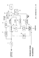
[発振周波数制御回路:図1]
本発明の実施の形態に係る発振周波数制御回路について図1を参照しながら説明する。図1は、本発明の実施の形態に係る発振周波数制御回路の構成ブロック図である。
本発明の実施の形態に係る発振周波数制御回路(本回路)は、図1に示すように、フィルタ11と、位相比較器12と、スイッチ13と、ループフィルタ14と、電圧制御発振器15と、分周器16と、検波回路17と、増幅器18と、CPU(Central Processing Unit)20と、メモリ21と、PWM(Pulse Width Modulation)回路22と、レベル検出回路23と、ADコンバータ24と、ADコンバータ25とから構成されている。
[Oscillation frequency control circuit: Fig. 1]
An oscillation frequency control circuit according to an embodiment of the present invention will be described with reference to FIG. FIG. 1 is a block diagram showing the configuration of an oscillation frequency control circuit according to an embodiment of the present invention.
As shown in FIG. 1, an oscillation frequency control circuit (this circuit) according to an embodiment of the present invention includes a
[本回路の各部]
フィルタ11は、例えば、10MHzの外部基準信号を帯域制限するフィルタである。基本構成として必須ではないが、外部基準信号の高周波成分を除去する働きがある。
位相比較器12は、フィルタ11から出力された基準信号と、分周器16で分周された信号の位相を比較し、位相差信号を出力する。
尚、位相比較器12は、外部基準信号と分周信号との位相を比較して同期(ロック)を検出した場合は、CPU20にロック検出信号を出力し、非同期(アンロック)を検出した場合は、CPU20にアンロック検出信号を出力する。
[Each part of this circuit]
The
The
When the
スイッチ13は、CPU20からの切替指示により、位相比較器12とループフィルタ14との接続のオン/オフを切り替える。つまり、CPU20からオンの指示が入力されると、位相比較器12からの出力をループフィルタ14に供給し、CPU20からオフの指示が入力されると、位相比較器12とループフィルタ14との接続を断とするものである。
The
ループフィルタ14は、位相比較器12からの出力電圧を平滑化するフィルタである。つまり、電圧制御発振器15の制御入力端子の電圧が平滑化されるものである。
電圧制御発振器15は、ループフィルタ14からの制御電圧によって周波数を変更して希望する周波数(内部基準信号)を発振出力する。
尚、電圧制御発振器(VCO)の代わりに、電圧制御付き水晶発振器(VCXO)、電圧制御機能付き恒温槽水晶発振器(VC−OCXO)等を用いてもよい。
The
The voltage controlled
In place of the voltage controlled oscillator (VCO), a crystal oscillator with voltage control (VCXO), a thermostat crystal oscillator with voltage control function (VC-OCXO), or the like may be used.
分周器16は、電圧制御発振器15から出力される内部基準信号を1/Nに分周する。
検波回路17は、フィルタ11からの出力信号のレベル検波を行う。
増幅器18は、検波回路17で検波された信号を増幅する。
The
The
The
CPU20は、ADコンバータ25からの制御電圧情報を入力し、最新の制御電圧情報としてメモリ21に記憶する。具体的には、CPU20は、ADコンバータ25から制御電圧情報が常時入力され、前回入力した制御電圧情報と変更がなければメモリ21の更新は行わず、変更があればメモリ21の制御電圧情報を更新する。
The
また、CPU20は、ADコンバータ24からの外部基準信号(外部REF)の検出されたレベルを入力し、メモリ21に記憶された適正範囲(第1のしきい値から第2のしきい値の間の範囲)内であるか否かを判定し、適正範囲内であればスイッチ13へはオンの指示を出力し、適正範囲外であればスイッチ13へはオフの指示を出力する。
Further, the
また、CPU20は、外部REFの検出レベルが適正範囲外であれば、メモリ21内に格納された電圧・PWMデューティーサイクルテーブルを参照し、現在(最新)の制御電圧の電圧情報に基づくPWMデューティーサイクルに従ったパルス幅の情報をPWM回路22に出力する。
Further, if the detection level of the external REF is out of the proper range, the
メモリ21は、最新の制御電圧情報、外部REFの検出レベルに対して適正範囲の基準となる第1のしきい値及び第2のしきい値、更に、電圧・PWMデューティーサイクルテーブルが記憶されている。
制御電圧情報は、レベル検出回路23で検出され、変更となった場合にメモリ21で更新され、最新の値として保持される。
The
The control voltage information is detected by the
[電圧・PWMデューティーサイクルテーブル:図2]
ここで、電圧・PWMデューティーサイクルテーブルについて図2を参照しながら説明する。図2は、電圧・PWMデューティーサイクルテーブルの概略図である。
電圧・PWMデューティーサイクルテーブルは、図2に示すように、電圧情報に対してパルス幅を特定するためのPWMデューティーサイクル(%)が記憶されている。
[Voltage / PWM duty cycle table: Fig. 2]
Here, the voltage / PWM duty cycle table will be described with reference to FIG. FIG. 2 is a schematic diagram of a voltage / PWM duty cycle table.
As shown in FIG. 2, the voltage / PWM duty cycle table stores a PWM duty cycle (%) for specifying a pulse width for voltage information.
ここで、電圧情報は、ループフィルタ14をからの制御電圧の値(制御電圧情報)を維持するために、PWM回路22からループフィルタ14に出力されるパルスのPWMデューティーサイクルを予め定めたものとなっている。
従って、レベル検出回路23で検出された制御電圧情報に対応するPWMデューティーサイクルを電圧・PWMデューティーサイクルテーブルから読み取り、そのサイクルに応じたパルスをPWM回路22がループフィルタ14に出力すると、ループフィルタ14から以前と同様の制御電圧が電圧制御発振器15に出力される。
Here, the voltage information is obtained by predetermining the PWM duty cycle of the pulse output from the
Accordingly, when the PWM duty cycle corresponding to the control voltage information detected by the
PWM回路22は、CPU20から入力されるPWMデューティーサイクルのデータをパルス幅変調して所望のパルス信号をループフィルタ14に出力する。CPU20から電圧情報のデータが出力されるのであれば、PWM回路に代えてDA(Digital/Analog)コンバータを用いることができる。
The
レベル検出回路23は、ループフィルタ14から出力される直流電圧を検出して制御電圧情報としてADコンバータ25に出力する。
ADコンバータ24は、増幅器18から出力された外部REFの検出レベルをアナログ信号からデジタル信号に変換してCPU20に出力する。
ADコンバータ25は、レベル検出回路23からの制御電圧情報をアナログ信号からデジタル信号に変換してCPU20に入力する。
The
The
The
尚、本回路において、外部基準信号の入力異常については、検波回路17及び増幅器18から出力される外部REFの検出レベルによってCPU20は、認識できるため、位相比較器12からのアンロック検出信号は用いていない。
In this circuit, the input abnormality of the external reference signal can be recognized by the
[本回路の動作]
本回路における動作について説明する。
本回路は、正常時、スイッチ13はオンで位相比較器12とループフィルタ14は接続された状態となっている。そして、位相比較器12は、外部基準信号と分周器16からの信号の位相差の信号を、ループフィルタ14を介して電圧制御発振器15に出力し、電圧制御発振器15における発振周波数を制御している。この際、レベル検出回路23は、最新の制御電圧を検出し、ADコンバータ25を介してCPU20に出力し、CPU20は、制御電圧情報に変更があれば、メモリ21で最新の制御電圧情報を更新する。
[Operation of this circuit]
The operation in this circuit will be described.
In this circuit, when the switch is normal, the
そして、本回路において、外部基準信号は、検波回路17で検波され、増幅器18で増幅されて、外部REFのレベルが検出され、ADコンバータ24を介してCPU20に出力される。
In this circuit, the external reference signal is detected by the
CPU20では、入力された外部REFの検出レベルが適正範囲内であるか否かを判定する。具体的には、メモリ21に記憶された適正範囲を示す第1のしきい値と第2のしきい値との間に外部REFの検出レベルの値があれば適正範囲内と判定し、第1のしきい値と第2のしきい値との間に外部REFの検出レベルの値がなければ適正範囲外と判定する。
The
判定結果、CPU20は、適正範囲内であれば、正常状態としてスイッチ13をオン状態に維持し、適正範囲外であれば、異常状態としてスイッチ13をオフ状態として、位相比較器12とループフィルタ14との接続を断とする。
As a result of the determination, if the
更に、異常状態では、CPU20は、メモリ21に記憶された最新の制御電圧情報を読み取り、その電圧情報に対応するPMWデューティーサイクルを電圧・PMWデューティーサイクルテーブルから読み取り、そのPWMデューティーサイクルとなるパルスを形成するための情報(データ)をPWM回路22に出力する。
PWM回路22は、CPU20から入力されたパルス形成の情報に従ってパルスを生成し、ループフィルタ14を介して電圧制御発振器15に制御電圧を出力する。
Further, in an abnormal state, the
The
これにより、外部基準信号に異常が発生した場合、特に、外部基準信号の入力がなくなった場合(自走の場合)等に、CPU20は、検波回路17、増幅器18からの出力により直ちに異常を検出し、位相比較器12の出力を切断して、これまで電圧制御発振器15を制御していた制御電圧と同様のパルスをPWM回路22から出力するものである。
つまり、位相比較器12の出力に代えて、PWM回路22からの出力を用いることで、これまでの状態を引き継いで電圧制御発振器15での周波数発振を適正化できるものである。
As a result, when an abnormality occurs in the external reference signal, particularly when no external reference signal is input (in the case of self-running), the
That is, by using the output from the
[別の実施の形態1]
尚、上記例では、PWM回路22から出力されるパルスを、レベル検出回路23で検出された最新の制御電圧情報に基づいて生成するようにしたが、デフォルトの電圧情報を記憶し、そのデフォルトの電圧情報に対応するPWMデューティーサイクルに基づいてパルス生成の情報を出力するようにしてもよい。
[Another embodiment 1]
In the above example, the pulse output from the
具体的には、メモリ21には、電圧制御発振器15に対する制御電圧において、その適正範囲内の中心電圧値を記憶しておき、それに対応するPWMデューティーサイクルは、50%となるから、電圧制御発振器14の制御電圧が0〜3.3Vで動作するのであれば、3.3/2Vの制御電圧に設定する。尚、中心電圧値以外の任意の電圧値を記憶して対応する制御電圧を設定してもよい。
デフォルトの電圧情報を用いれば、レベル検出回路23及びADコンバータ25の部品、メモリ21内の電圧・PMWデューティーサイクルテーブルを不要とすることができる。
Specifically, in the control voltage for the voltage controlled
If the default voltage information is used, the components of the
[校正]
本回路における校正について図3を参照しながら説明する。図3は、校正時の特性を示す図である。
本回路において、図3に示すように、外部基準信号が入力されない状態で時間が経過すると、周波数偏差が上昇又は下降する。図では上昇を示している。そこで、特定のタイミングで、適正な基準信号を入力して、その後、基準信号の入力を停止すると、自走制御により周波数偏差が中心周波数に戻ってきて校正が為されるようになっている。図3では、校正を2回繰り返している。
[Proofreading]
Calibration in this circuit will be described with reference to FIG. FIG. 3 is a diagram showing characteristics at the time of calibration.
In this circuit, as shown in FIG. 3, when time passes without an external reference signal being input, the frequency deviation increases or decreases. The figure shows a rise. Therefore, when an appropriate reference signal is input at a specific timing and then the input of the reference signal is stopped, the frequency deviation returns to the center frequency by self-running control, and calibration is performed. In FIG. 3, the calibration is repeated twice.
この校正では、電圧制御発振器15に対する制御電圧の制御範囲内における中心電圧値を用いて周波数制御を行っている。
本回路によれば、校正時に特別な回路を接続しなくても、校正作業を行うことができる効果がある。
In this calibration, frequency control is performed using the center voltage value within the control range of the control voltage for the voltage controlled
According to this circuit, the calibration work can be performed without connecting a special circuit during calibration.
[経年変化の電圧特性:図4]
次に、本回路における経年変化に対する最適な制御電圧特性例を図4に示す。図4は、経年変化・制御電圧特性を示す図である。
図4に示すように、本回路においては、時間の経過と共に、最適な制御電圧が小さくなっている(但し、周波数偏差として上昇する場合を示している)。
[Voltage characteristics of aging: Fig. 4]
Next, FIG. 4 shows an example of optimum control voltage characteristics with respect to secular change in this circuit. FIG. 4 is a diagram showing aging / control voltage characteristics.
As shown in FIG. 4, in this circuit, the optimum control voltage decreases with time (however, the case where the frequency deviation increases) is shown.
[別の実施の形態2]
更に、別の実施の形態(別の実施の形態2)として、本回路を上記経年変化に対応した構成とするものである。この別の実施の形態2について図5を参照しながら説明する。図5は、経年変化特性テーブルの概略図である。
本回路において、メモリ21には、電圧・PMWデューティーサイクルテーブルが格納されているが、そのテーブルの代わりに、図5の経年変化特性テーブルを利用するものである。
[Another embodiment 2]
Furthermore, as another embodiment (another embodiment 2), this circuit has a configuration corresponding to the above-mentioned secular change. Another
In this circuit, the
図5の経年変化特性テーブルは、電圧情報とPWMデューティーサイクルの関係に、更に時間のファクタを設けている。
具体的には、時間の経過に対して適正な電圧情報が設定され、更にその電圧情報に対応してPWMデューティーサイクルが設定されてテーブルとして記憶されている。
CPU20は、内部にタイマーを備え、時間の経過を測定している。
The aging characteristic table of FIG. 5 further provides a time factor in the relationship between the voltage information and the PWM duty cycle.
Specifically, voltage information appropriate for the passage of time is set, and a PWM duty cycle is set corresponding to the voltage information and stored as a table.
The
別の実施の形態2では、外部基準信号の検出レベルが適正範囲外であるときに、CPU20が、スイッチ13をオフにし、内部のタイマーで測定している時間を参照し、当該時間に対応する電圧情報からPWMデューティーサイクルを検索し、当該PWMデューティーサイクルに従ったパルスを生成するための情報をPWM回路22に出力し、PWM回路22で所望のパルスを生成してループフィルタ14を介して電圧制御発振器15に制御電圧を出力するものである。
In another
これにより、別の実施の形態2では、CPU20が、外部基準信号の異常時に経年変化に対応した電圧情報、それに応じたPWMデューティーサイクルに従って生成したパルスにより発振周波数の補正を行うようにしているので、周波数制御回路を経年変化に対応させることができる効果がある。
As a result, in another
また、別の実施の形態2における回路構成において、校正を行うようにしてもよい。
この場合、CPU20は時間経過を計測しており、校正作業のときは経年変化特性テーブルを参照して時間経過に対応した電圧値を用いて周波数制御を行う。これにより、校正作業を周波数制御回路の経年変化に対応させることができる効果がある。
Further, calibration may be performed in the circuit configuration according to the second embodiment.
In this case, the
本発明は、自己の周波数を補正し、高安定な基準信号の入力がなく、自走したときでも発振周波数を安定に保つことができる発振周波数制御回路に好適である。 The present invention is suitable for an oscillation frequency control circuit that corrects its own frequency, does not receive a highly stable reference signal, and can keep the oscillation frequency stable even when it is free-running.
11…フィルタ、 12…位相比較器、 13…スイッチ、 14…ループフィルタ、 15…電圧制御発振器、 16…分周器、 17…検波回路、 18…増幅器、 20…CPU、 21…メモリ、 22…PWM回路、 23…レベル検出回路、 24…ADコンバータ、 25…ADコンバータ、 32…位相比較器、 33…チャージポンプ、 34…ループフィルタ、 35…VCXO、 36…分周器
DESCRIPTION OF
Claims (6)
外部基準信号と前記分周器からの出力の位相を比較し、位相差信号を出力する位相比較器と、
前記位相比較器からの出力を平滑化して前記電圧制御発振器に制御電圧を出力するループフィルタと、
前記ループフィルタからの出力について電圧レベルを検出して最新の制御電圧情報を出力するレベル検出回路と、
外部基準信号を検波する検波回路と、
パルス生成の情報が入力されるとパルスを生成して前記ループフィルタに出力するパルス生成回路と、
前記電圧制御発振器に出力される制御電圧の値を制御電圧情報として、複数の制御電圧情報とそれに対応するパルス生成の情報を記憶する電圧・パルス生成の情報テーブルを記憶し、前記レベル検出回路で検出された電圧レベルを最新の制御電圧情報として記憶するメモリと、
前記位相比較器と前記ループフィルタとの接続をオン/オフするスイッチと、
前記レベル検出回路で検出された電圧レベルを入力し、当該電圧レベルを最新の制御電圧情報として前記メモリに記憶されている最新の制御電圧情報を更新すると共に、前記検波回路で検出された外部基準信号のレベルが適正範囲内であれば前記スイッチをオンとし、前記レベルが適正範囲外であれば前記スイッチをオフとして前記メモリに記憶された更新された最新の制御電圧情報を読み取り、当該最新の制御電圧情報に対応するパルス生成の情報を前記電圧・パルス生成の情報テーブルから読み取り、当該パルス生成の情報を前記パルス生成回路に出力する制御部とを有し、
前記パルス生成回路は、パルス幅変調回路であり、前記制御部から出力されるパルス生成の情報は、パルス幅変調デューティーサイクルの情報であることを特徴とする発振周波数制御回路。 A voltage controlled oscillator, and a frequency divider for dividing the output from the voltage controlled oscillator;
A phase comparator that compares the phase of the output from the frequency divider with an external reference signal, and outputs a phase difference signal;
A loop filter that smoothes the output from the phase comparator and outputs a control voltage to the voltage controlled oscillator;
A level detection circuit that detects the voltage level of the output from the loop filter and outputs the latest control voltage information;
A detection circuit for detecting an external reference signal;
A pulse generation circuit that generates a pulse when pulse generation information is input and outputs the pulse to the loop filter;
As the control voltage information the value of the control voltage output to the voltage controlled oscillator, and stores information table of the voltage pulse generator for storing the pulse generation information corresponding thereto and a plurality of control voltage information, the level detection circuit A memory for storing the voltage level detected in step 1 as the latest control voltage information ;
A switch for turning on / off the connection between the phase comparator and the loop filter;
The voltage level detected by the level detection circuit is input, the latest control voltage information stored in the memory is updated with the voltage level as the latest control voltage information, and the external reference detected by the detection circuit If the signal level is within the proper range, the switch is turned on, and if the level is outside the proper range, the switch is turned off and the latest control voltage information stored in the memory is read, and the latest A control unit that reads pulse generation information corresponding to control voltage information from the voltage / pulse generation information table and outputs the pulse generation information to the pulse generation circuit;
The pulse generation circuit is a pulse width modulation circuit, and the pulse generation information output from the control unit is information of a pulse width modulation duty cycle.
制御部は、内部にタイマーを備えて時間を計測し、外部基準信号のレベルが適正範囲外であるときに、前記メモリの経年変化特性テーブルから計測した時間に応じた制御電圧情報を検索し、検索した制御電圧情報に対応するパルス生成の情報を読み取り、パルス生成回路に出力することを特徴とする請求項1記載の発振周波数制御回路。 The memory stores the aging characteristics table storing proper control voltage information and the pulse generation information corresponding thereto with respect to time warp the year change,
The control unit includes a timer inside to measure time, and when the level of the external reference signal is outside the appropriate range, retrieves control voltage information according to the measured time from the aging characteristic table of the memory, 2. The oscillation frequency control circuit according to claim 1, wherein information on pulse generation corresponding to the searched control voltage information is read and output to the pulse generation circuit.
Priority Applications (7)
| Application Number | Priority Date | Filing Date | Title |
|---|---|---|---|
| JP2006349519A JP4374463B2 (en) | 2006-12-26 | 2006-12-26 | Oscillation frequency control circuit |
| KR1020087030507A KR101077730B1 (en) | 2006-12-26 | 2007-10-31 | Oscillation frequency control circuit |
| PCT/JP2007/071209 WO2008078452A1 (en) | 2006-12-26 | 2007-10-31 | Oscillation frequency control circuit |
| EP07830943A EP2066035B1 (en) | 2006-12-26 | 2007-10-31 | Oscillation frequency control circuit |
| BRPI0717254-0A BRPI0717254A2 (en) | 2006-12-26 | 2007-10-31 | OSCILLATION FREQUENCY CONTROL CIRCUIT |
| CN2007800258242A CN101490960B (en) | 2006-12-26 | 2007-10-31 | Oscillation frequency control circuit |
| US12/320,321 US20090134946A1 (en) | 2006-12-26 | 2009-01-23 | Oscillation frequency control circuit |
Applications Claiming Priority (1)
| Application Number | Priority Date | Filing Date | Title |
|---|---|---|---|
| JP2006349519A JP4374463B2 (en) | 2006-12-26 | 2006-12-26 | Oscillation frequency control circuit |
Publications (3)
| Publication Number | Publication Date |
|---|---|
| JP2008160677A JP2008160677A (en) | 2008-07-10 |
| JP2008160677A5 JP2008160677A5 (en) | 2008-11-06 |
| JP4374463B2 true JP4374463B2 (en) | 2009-12-02 |
Family
ID=39562246
Family Applications (1)
| Application Number | Title | Priority Date | Filing Date |
|---|---|---|---|
| JP2006349519A Active JP4374463B2 (en) | 2006-12-26 | 2006-12-26 | Oscillation frequency control circuit |
Country Status (7)
| Country | Link |
|---|---|
| US (1) | US20090134946A1 (en) |
| EP (1) | EP2066035B1 (en) |
| JP (1) | JP4374463B2 (en) |
| KR (1) | KR101077730B1 (en) |
| CN (1) | CN101490960B (en) |
| BR (1) | BRPI0717254A2 (en) |
| WO (1) | WO2008078452A1 (en) |
Families Citing this family (10)
| Publication number | Priority date | Publication date | Assignee | Title |
|---|---|---|---|---|
| CN101651456B (en) | 2008-08-12 | 2012-03-21 | 博通集成电路(上海)有限公司 | Circuit for recovering clock signals |
| JP5277919B2 (en) * | 2008-12-10 | 2013-08-28 | 株式会社Jvcケンウッド | Reference signal oscillation device and reference signal oscillation method |
| JP5198316B2 (en) * | 2009-02-19 | 2013-05-15 | 富士通セミコンダクター株式会社 | PLL circuit and oscillation device |
| US20100220006A1 (en) * | 2009-02-27 | 2010-09-02 | Amir Arab | Global positioning systems based disciplined reference clock |
| CN101841329A (en) * | 2010-06-12 | 2010-09-22 | 中兴通讯股份有限公司 | Phase-locked loop, and voltage-controlled device and method |
| CN104467123B (en) * | 2014-12-31 | 2017-08-08 | 展讯通信(上海)有限公司 | Charging method, device, charger, electronic installation and equipment |
| JP2017194789A (en) * | 2016-04-19 | 2017-10-26 | ローム株式会社 | Clock generation device, electronic circuit, integrated circuit, and electrical appliance |
| JP2018085563A (en) | 2016-11-21 | 2018-05-31 | ソニーセミコンダクタソリューションズ株式会社 | Oscillator and oscillation method |
| EP3573241B1 (en) * | 2018-05-24 | 2022-08-03 | The Swatch Group Research and Development Ltd | Reference oscillator with variable duty cycle, frequency synthesiser and signal receiver with the reference oscillator |
| JP6826165B1 (en) * | 2019-08-06 | 2021-02-03 | 株式会社京三製作所 | Pulsed high frequency monitor |
Family Cites Families (15)
| Publication number | Priority date | Publication date | Assignee | Title |
|---|---|---|---|---|
| JPH01222519A (en) * | 1988-03-01 | 1989-09-05 | Toyo Commun Equip Co Ltd | Control system for oscillation circuit |
| JPH0450935U (en) * | 1990-09-06 | 1992-04-28 | ||
| FI91821C (en) * | 1991-02-22 | 1994-08-10 | Nokia Mobile Phones Ltd | Automatic frequency control switching of the radio telephone |
| JPH04369927A (en) * | 1991-06-19 | 1992-12-22 | Hitachi Ltd | Pll oscillator |
| US5334952A (en) * | 1993-03-29 | 1994-08-02 | Spectralink Corporation | Fast settling phase locked loop |
| JP2581398B2 (en) * | 1993-07-12 | 1997-02-12 | 日本電気株式会社 | PLL frequency synthesizer |
| IL120119A0 (en) | 1997-01-31 | 1997-04-15 | Binder Yehuda | Method and system for calibrating a crystal oscillator |
| US6345079B1 (en) * | 1997-10-29 | 2002-02-05 | Victor Company Of Japan, Ltd. | Clock signal generation apparatus |
| US6313708B1 (en) * | 2000-07-26 | 2001-11-06 | Marconi Communications, Inc. | Analog phase locked loop holdover |
| US6914489B2 (en) * | 2002-09-26 | 2005-07-05 | Koninklijke Philips Electronics N.V. | Voltage-controlled oscillator presetting circuit |
| US7015762B1 (en) * | 2004-08-19 | 2006-03-21 | Nortel Networks Limited | Reference timing signal apparatus and method |
| JP2006121171A (en) * | 2004-10-19 | 2006-05-11 | Matsushita Electric Ind Co Ltd | Clock supplying device with frequency correction function |
| US8022773B2 (en) * | 2004-12-17 | 2011-09-20 | Mitsubishi Electric Corporation | Clock signal generation device, and wireless base station |
| JP4424546B2 (en) * | 2005-01-13 | 2010-03-03 | Okiセミコンダクタ株式会社 | Pulse width modulation circuit |
| JP4625494B2 (en) * | 2007-12-25 | 2011-02-02 | 日本電波工業株式会社 | Oscillation frequency control circuit |
-
2006
- 2006-12-26 JP JP2006349519A patent/JP4374463B2/en active Active
-
2007
- 2007-10-31 BR BRPI0717254-0A patent/BRPI0717254A2/en not_active IP Right Cessation
- 2007-10-31 KR KR1020087030507A patent/KR101077730B1/en not_active IP Right Cessation
- 2007-10-31 CN CN2007800258242A patent/CN101490960B/en active Active
- 2007-10-31 WO PCT/JP2007/071209 patent/WO2008078452A1/en active Application Filing
- 2007-10-31 EP EP07830943A patent/EP2066035B1/en active Active
-
2009
- 2009-01-23 US US12/320,321 patent/US20090134946A1/en not_active Abandoned
Also Published As
| Publication number | Publication date |
|---|---|
| US20090134946A1 (en) | 2009-05-28 |
| BRPI0717254A2 (en) | 2013-10-08 |
| CN101490960B (en) | 2013-01-02 |
| EP2066035A1 (en) | 2009-06-03 |
| KR20090026146A (en) | 2009-03-11 |
| EP2066035B1 (en) | 2012-09-12 |
| EP2066035A4 (en) | 2010-09-29 |
| WO2008078452A1 (en) | 2008-07-03 |
| KR101077730B1 (en) | 2011-10-27 |
| CN101490960A (en) | 2009-07-22 |
| JP2008160677A (en) | 2008-07-10 |
Similar Documents
| Publication | Publication Date | Title |
|---|---|---|
| JP4374463B2 (en) | Oscillation frequency control circuit | |
| JP4625494B2 (en) | Oscillation frequency control circuit | |
| US7332979B2 (en) | Low noise reference oscillator with fast start-up | |
| US8248113B2 (en) | Method and apparatus for accurate clock synthesis | |
| JP4355350B2 (en) | Oscillation frequency control circuit | |
| US8766736B2 (en) | Methods of frequency versus temperature compensation of existing crystal oscillators | |
| US20130285753A1 (en) | Automatic self-calibrated oscillation method and apparatus using the same | |
| KR101515099B1 (en) | Charge pump charge pump calibration apparatus and phase lock loop comprising the same | |
| JP5145398B2 (en) | Oscillation frequency control circuit | |
| US7151414B2 (en) | Method and circuit for frequency synthesis using a low drift current controlled oscillator with wide output frequency range | |
| JP5027265B2 (en) | PLL device | |
| JP5426316B2 (en) | Frequency synthesizer | |
| JP2011040967A (en) | Pll circuit | |
| US11829198B2 (en) | Clock circuit portions | |
| JP5063833B2 (en) | High-frequency signal generator based on the time base of the clock | |
| US20060034409A1 (en) | Digital vco and pll circuit using the digital vco | |
| JP2000323987A (en) | Pll circuit | |
| JP2004172686A (en) | Reference signal generator | |
| JPH09321621A (en) | Frequency synthesizer | |
| JPH1065528A (en) | Pll circuit |
Legal Events
| Date | Code | Title | Description |
|---|---|---|---|
| A521 | Request for written amendment filed |
Free format text: JAPANESE INTERMEDIATE CODE: A523 Effective date: 20080919 |
|
| A621 | Written request for application examination |
Free format text: JAPANESE INTERMEDIATE CODE: A621 Effective date: 20080919 |
|
| A871 | Explanation of circumstances concerning accelerated examination |
Free format text: JAPANESE INTERMEDIATE CODE: A871 Effective date: 20080919 |
|
| A975 | Report on accelerated examination |
Free format text: JAPANESE INTERMEDIATE CODE: A971005 Effective date: 20081003 |
|
| A131 | Notification of reasons for refusal |
Free format text: JAPANESE INTERMEDIATE CODE: A131 Effective date: 20081125 |
|
| A521 | Request for written amendment filed |
Free format text: JAPANESE INTERMEDIATE CODE: A523 Effective date: 20090123 |
|
| A131 | Notification of reasons for refusal |
Free format text: JAPANESE INTERMEDIATE CODE: A131 Effective date: 20090421 |
|
| A521 | Request for written amendment filed |
Free format text: JAPANESE INTERMEDIATE CODE: A523 Effective date: 20090618 |
|
| TRDD | Decision of grant or rejection written | ||
| A01 | Written decision to grant a patent or to grant a registration (utility model) |
Free format text: JAPANESE INTERMEDIATE CODE: A01 Effective date: 20090818 |
|
| A01 | Written decision to grant a patent or to grant a registration (utility model) |
Free format text: JAPANESE INTERMEDIATE CODE: A01 |
|
| A61 | First payment of annual fees (during grant procedure) |
Free format text: JAPANESE INTERMEDIATE CODE: A61 Effective date: 20090820 |
|
| R150 | Certificate of patent or registration of utility model |
Ref document number: 4374463 Country of ref document: JP Free format text: JAPANESE INTERMEDIATE CODE: R150 Free format text: JAPANESE INTERMEDIATE CODE: R150 |
|
| FPAY | Renewal fee payment (event date is renewal date of database) |
Free format text: PAYMENT UNTIL: 20120918 Year of fee payment: 3 |
|
| FPAY | Renewal fee payment (event date is renewal date of database) |
Free format text: PAYMENT UNTIL: 20120918 Year of fee payment: 3 |
|
| FPAY | Renewal fee payment (event date is renewal date of database) |
Free format text: PAYMENT UNTIL: 20120918 Year of fee payment: 3 |
|
| FPAY | Renewal fee payment (event date is renewal date of database) |
Free format text: PAYMENT UNTIL: 20130918 Year of fee payment: 4 |
|
| R250 | Receipt of annual fees |
Free format text: JAPANESE INTERMEDIATE CODE: R250 |
|
| R250 | Receipt of annual fees |
Free format text: JAPANESE INTERMEDIATE CODE: R250 |
|
| R250 | Receipt of annual fees |
Free format text: JAPANESE INTERMEDIATE CODE: R250 |
|
| S531 | Written request for registration of change of domicile |
Free format text: JAPANESE INTERMEDIATE CODE: R313531 |
|
| R350 | Written notification of registration of transfer |
Free format text: JAPANESE INTERMEDIATE CODE: R350 |
|
| R250 | Receipt of annual fees |
Free format text: JAPANESE INTERMEDIATE CODE: R250 |
|
| R250 | Receipt of annual fees |
Free format text: JAPANESE INTERMEDIATE CODE: R250 |
|
| R250 | Receipt of annual fees |
Free format text: JAPANESE INTERMEDIATE CODE: R250 |
|
| R250 | Receipt of annual fees |
Free format text: JAPANESE INTERMEDIATE CODE: R250 |
|
| R250 | Receipt of annual fees |
Free format text: JAPANESE INTERMEDIATE CODE: R250 |
|
| R250 | Receipt of annual fees |
Free format text: JAPANESE INTERMEDIATE CODE: R250 |
|
| R250 | Receipt of annual fees |
Free format text: JAPANESE INTERMEDIATE CODE: R250 |
|
| R250 | Receipt of annual fees |
Free format text: JAPANESE INTERMEDIATE CODE: R250 |
|
| R250 | Receipt of annual fees |
Free format text: JAPANESE INTERMEDIATE CODE: R250 |