JP4370880B2 - Optical element manufacturing method, recording and / or reproducing apparatus, and optical microscope apparatus - Google Patents
Optical element manufacturing method, recording and / or reproducing apparatus, and optical microscope apparatus Download PDFInfo
- Publication number
- JP4370880B2 JP4370880B2 JP2003374676A JP2003374676A JP4370880B2 JP 4370880 B2 JP4370880 B2 JP 4370880B2 JP 2003374676 A JP2003374676 A JP 2003374676A JP 2003374676 A JP2003374676 A JP 2003374676A JP 4370880 B2 JP4370880 B2 JP 4370880B2
- Authority
- JP
- Japan
- Prior art keywords
- optical
- lens
- probe
- light beam
- light
- Prior art date
- Legal status (The legal status is an assumption and is not a legal conclusion. Google has not performed a legal analysis and makes no representation as to the accuracy of the status listed.)
- Expired - Fee Related
Links
Images


Landscapes
- Microscoopes, Condenser (AREA)
- Lenses (AREA)
- Optical Head (AREA)
Description
本発明は、近接場光を利用した光学素子の製造方法、このような光学素子を搭載した光学ヘッドを用いた記録及び/又は再生装置及び光学顕微鏡装置に関する。 The present invention relates to a method of manufacturing an optical device using the near-field light, a recording and / or reproducing apparatus and an optical microscope apparatus using an optical head having an optical element mounted such as this.
近年、磁気ディスクや光ディスク等の記録媒体における記録密度の増加には著しいものがある。特に、光記録媒体の場合には、高記録密度化に対応して様々な記録再生方式が提案されている。例えば、ソリッド・イマージョン・レンズ(Solid Immersion Lens:以下、SILと称する。)やソリッド・イマージョン・ミラー(Solid Immersion Mirror:以下、SIMと称する。)等を光学素子として用い、近接場(ニアフィールド)によるエバネッセント波を利用して、これまでの回折限界を超える高NAでの再生を可能としている。 In recent years, there has been a remarkable increase in recording density in recording media such as magnetic disks and optical disks. In particular, in the case of optical recording media, various recording / reproducing systems have been proposed in response to higher recording densities. For example, a solid immersion lens (hereinafter referred to as SIL), a solid immersion mirror (hereinafter referred to as SIM) or the like is used as an optical element, and a near field (near field). By using the evanescent wave by, reproduction with a high NA exceeding the conventional diffraction limit is made possible.
しかしながら、光記録媒体において、1テラビット/インチ2を超える記録密度を実現することは、物理的な制約のため非常に困難であると考えられている。特に、SILの場合、半球レンズに集光される光ビームのスポット径は、λ/NA(λ:波長,NA:開口数)で決まり、レンズの高NA化や光ビームの短波長化を考えても、スポット径を100nm以下まで低減することは困難である。 However, it is considered very difficult to achieve a recording density exceeding 1 terabit / inch 2 in an optical recording medium due to physical limitations. In particular, in the case of SIL, the spot diameter of the light beam collected on the hemispherical lens is determined by λ / NA (λ: wavelength, NA: numerical aperture), and considering higher lens NA and shorter light beam wavelength. However, it is difficult to reduce the spot diameter to 100 nm or less.
一方、光記録媒体の記録密度の限界を超える方法として、近接場光学顕微鏡(Scanning Near-field Optical Microscope:以下、SNOMと称する。)を用い、ナノメータオーダのドメインを記録再生する方法が提案されている。その中でも、特にSIAM(Scanning Interferometric Apertureless Microscope)方式では、外部照明光の中に金属プローブ(AFMカンチレバー)を配置し、このプローブ周辺に生じる近接場光を用いた検出を行うことで、従来のSNOMに比べて、1nm程度の高分解能での検出を可能としている(例えば、非特許文献1,2を参照。)。
On the other hand, as a method of exceeding the recording density limit of an optical recording medium, a method of recording and reproducing a nanometer order domain using a scanning near-field optical microscope (hereinafter referred to as SNOM) has been proposed. Yes. In particular, in the SIAM (Scanning Interferometric Apertureless Microscope) system, a metal probe (AFM cantilever) is placed in the external illumination light, and detection using the near-field light generated around this probe is performed, so that the conventional SNOM is performed. Compared to the above, detection with a high resolution of about 1 nm is possible (for example, see Non-Patent
これらSNOM技術は、いわゆる原子間力顕微鏡(Atomic Force Microscope:以下、AFMと称する。)をベースとした技術であり、このAFMを用いるメモリにおいては、AFMチップ先端の接触摩耗や、カンチレバーの共振周波数等の機械的な理由から、データレートの高速化を実現することは困難である。また、AFMチップ先端の接触摩耗によって、検出感度が低下してしまうことから、AFMメモリの高信頼性を実現することは極めて困難である。 These SNOM technologies are based on a so-called atomic force microscope (hereinafter referred to as AFM), and in a memory using this AFM, contact wear at the tip of the AFM tip and the resonance frequency of the cantilever. For mechanical reasons such as these, it is difficult to increase the data rate. In addition, since the detection sensitivity is reduced due to contact wear at the tip of the AFM tip, it is extremely difficult to achieve high reliability of the AFM memory.
そこで、この問題を解決する方法として、レンズにプローブを埋め込むという方法が提案されている(例えば、特許文献1を参照。)。しかしながら、上記特許文献1には、半球状レンズの下面にトレンチ溝を形成し、このトレンチ溝にプローブ膜を埋め込むことによって、プローブを形成するという方法が提案されているものの、トレンチ溝の深さは、一般に数10〜100nm程度であり、この面に摺動摩耗が生じた場合、プローブの摩耗によって検出感度が低下してしまう。このため、光学素子の信頼性を確保することは非常に困難である。
Therefore, as a method for solving this problem, a method of embedding a probe in a lens has been proposed (see, for example, Patent Document 1). However, although
そこで、本発明は、このような従来の事情に鑑みて提案されたものであり、従来の光学系で集光される光ビームのスポットよりも微小なマークを検出し得ると共に、プローブの摩耗による影響を受けることなく、高分解能での検出が可能な光学素子を搭載した光学ヘッドを用いた記録及び/又は再生装置を提供することを目的とする。 Therefore, the present invention has been proposed in view of such a conventional situation, and can detect a mark smaller than a spot of a light beam collected by a conventional optical system, and also by wear of a probe. It is an object of the present invention to provide a recording and / or reproducing apparatus using an optical head equipped with an optical element that can be detected with high resolution without being affected.
また、本発明は、そのような信頼性の高い光学素子を容易に作製可能であり且つ再現性に優れた光学素子の製造方法を提供することを目的とする。 It is another object of the present invention to provide a method for manufacturing an optical element that can easily produce such a highly reliable optical element and has excellent reproducibility.
また、本発明は、そのような光学素子を搭載することによって、検出感度及び検出速度の大幅な向上を可能とした光学ヘッドを用いた記録及び/又は再生装置を提供することを目的とする。 Another object of the present invention is to provide a recording and / or reproducing apparatus using an optical head that can significantly improve detection sensitivity and detection speed by mounting such an optical element.
また、本発明は、そのような光学ヘッドを用いて、光記録媒体に対する信号の記録及び/又は再生を高密度に行うことを可能とした記録及び/又は再生装置を提供することを目的とする。 It is another object of the present invention to provide a recording and / or reproducing apparatus capable of recording and / or reproducing signals on an optical recording medium with high density using such an optical head. .
また、本発明は、そのような光学ヘッドを用いて、試料に対する観察を高分解能で行うことを可能とした光学顕微鏡装置を提供することを目的とする。 It is another object of the present invention to provide an optical microscope apparatus that can perform observation on a sample with high resolution using such an optical head.
本発明に係る光学素子の製造方法は、第1の光学ガラスの一主面上にプローブとなる膜を成膜した後に、各光学素子に対応した複数のプローブをリソグラフィ技術によりパターン形成するプローブ形成工程と、複数のプローブが形成された第1の光学ガラスと、この第1の光学ガラスと同質の第2の光学ガラスとを互いに突き合わされて接合される接合面の間に当該プローブが位置するように接合し、接合一体化された光学ガラスブロックを形成するブロック形成工程と、光学ガラスブロックに対して球面研磨加工を施すことによって、各光学素子毎に分割された球状のレンズ体を形成する球面研磨工程と、球状のレンズ体に対して平面研磨加工を施すことによって、接合面と直交する面をプローブの先端部が臨む位置まで平坦化し、この面を集光された光ビームの出射面とする半球状又は超半球状のレンズ体を形成する平面研磨工程とを有することを特徴としている。 The optical element manufacturing method according to the present invention includes a probe formation in which a film serving as a probe is formed on one main surface of a first optical glass, and then a plurality of probes corresponding to each optical element are patterned by a lithography technique. The probe is located between the bonding surface where the first optical glass on which the plurality of probes are formed and the second optical glass of the same quality as the first optical glass are abutted and bonded to each other. And forming a spherical lens body divided for each optical element by applying a spherical polishing process to the optical glass block. By subjecting the spherical polishing process and surface polishing to the spherical lens body, the surface orthogonal to the bonding surface is flattened to the position where the tip of the probe faces, and this surface It is characterized by having a surface polishing step of forming a hemispherical or hyper-hemispherical lens body and the exit surface of the collected light beam.
また、本発明に係る記録及び/又は再生装置は、近接場光を利用して光記録媒体に対する信号の記録及び/又は再生を行うものであり、光ビームを出射する光源と、光記録媒体に近接した状態で対向配置され、光源から出射された光ビームを集光させて光記録媒体の信号記録面に照射する光学ヘッドと、光記録媒体の信号記録面で反射された光ビームの光強度の変化を検出する光強度検出手段とを備える。また、光学ヘッドは、光源から出射された光ビームを集光させる対物レンズと、対物レンズにより集光される光ビームの光路中に配置された光学素子と、対物レンズ及び光学素子を支持する支持体とを備える。そして、光学素子は、第1のレンズ素子と第2のレンズ素子とが互いの接合面を突き合わせて接合されると共に、この接合面と直交する面を対物レンズにより集光された光ビームの出射面とするレンズ体と、第1のレンズ素子と第2のレンズ素子との間に配置されると共に、レンズ体の出射面に臨む先端部が当該レンズ体の出射面に集光される光ビームのスポットよりも小となるプローブとを備えることを特徴としている。 The recording and / or reproducing apparatus according to the present invention performs recording and / or reproduction of a signal on an optical recording medium using near-field light, and includes a light source that emits a light beam and an optical recording medium. An optical head that is disposed opposite to each other, condenses the light beam emitted from the light source and irradiates the signal recording surface of the optical recording medium, and the light intensity of the light beam reflected by the signal recording surface of the optical recording medium Light intensity detecting means for detecting a change in the light intensity. The optical head includes an objective lens for condensing the light beam emitted from the light source, an optical element disposed in the optical path of the light beam collected by the objective lens, and a support for supporting the objective lens and the optical element. With body. In the optical element, the first lens element and the second lens element are joined by abutting each other's joint surface, and the surface orthogonal to the joint surface is emitted by the objective lens. A light beam that is disposed between the lens body serving as a surface, the first lens element, and the second lens element, and whose front end facing the exit surface of the lens body is condensed on the exit surface of the lens body And a probe that is smaller than the spot.
また、本発明に係る光学顕微鏡装置は、近接場光を利用して試料の観察を行うものであり、光ビームを出射する光源と、試料と近接した状態で対向配置され、光源から出射された光ビームを集光させて試料の表面に照射する光学ヘッドと、試料の表面で反射された光ビームの光強度の変化を検出する光強度検出手段とを備える。また、光学ヘッドは、光源から出射された光ビームを集光させる対物レンズと、対物レンズにより集光される光ビームの光路中に配置された光学素子と、対物レンズ及び光学素子を支持する支持体とを備える。そして、光学素子は、第1のレンズ素子と第2のレンズ素子とが互いの接合面を突き合わせて接合されると共に、この接合面と直交する面を対物レンズにより集光された光ビームの出射面とするレンズ体と、第1のレンズ素子と第2のレンズ素子との間に配置されると共に、レンズ体の出射面に臨む先端部が当該レンズ体の出射面に集光される光ビームのスポットよりも小となるプローブとを備えることを特徴としている。 The optical microscope apparatus according to the present invention is for observing a sample using near-field light. The light microscope emits a light beam and is opposed to the sample in a state of being close to the sample and emitted from the light source. An optical head for condensing the light beam to irradiate the surface of the sample, and a light intensity detecting means for detecting a change in light intensity of the light beam reflected by the surface of the sample. The optical head includes an objective lens for condensing the light beam emitted from the light source, an optical element disposed in the optical path of the light beam collected by the objective lens, and a support for supporting the objective lens and the optical element. With body. In the optical element, the first lens element and the second lens element are joined by abutting each other's joint surface, and the surface orthogonal to the joint surface is emitted by the objective lens. A light beam that is disposed between the lens body serving as a surface, the first lens element, and the second lens element, and whose front end facing the exit surface of the lens body is condensed on the exit surface of the lens body And a probe that is smaller than the spot.
以上のように、本発明に用いる光学素子では、プローブのレンズ体の出射面に臨む先端部が当該レンズ体の出射面に集光される光ビームのスポットよりも小となることから、当該光ビームのスポットよりも微小なマークを検出することが可能である。また、プローブは、互いの接合面を突き合わせて接合される第1のレンズ素子と第2のレンズ素子との間に配置されることから、この接合面と直交する光ビームの出射面に臨む当該プローブの先端部を光軸方向に長尺且つ微細な形状とすることが可能である。したがって、プローブの先端部の摩耗による影響を受けることなく、高分解能での検出が可能となり、信頼性を大幅に向上させることが可能である。 As described above, in the optical element used in the present invention , the tip of the probe facing the exit surface of the lens body is smaller than the spot of the light beam collected on the exit surface of the lens body. It is possible to detect a mark smaller than the beam spot. In addition, since the probe is disposed between the first lens element and the second lens element that are joined by abutting each other's joint surface, the probe faces the light beam emission surface orthogonal to the joint surface. The tip of the probe can be elongated and fine in the optical axis direction. Therefore, detection with high resolution is possible without being affected by wear of the tip of the probe, and reliability can be greatly improved.
また、本発明に係る光学素子の製造方法では、レンズ体の出射面に集光される光ビームのスポットよりも微小なマークを検出し得ると共に、プローブの先端部の摩耗による影響を受けることなく、高分解能での検出が可能な信頼性の高い上記光学素子を容易且つ再現性に優れた方法で一括作製することが可能である。 Further, in the method for manufacturing an optical element according to the present invention, it is possible to detect a mark smaller than the spot of the light beam collected on the exit surface of the lens body, and without being affected by the wear of the probe tip. The above-described highly reliable optical element that can be detected with high resolution can be manufactured in a batch by an easy and excellent reproducibility method.
また、本発明に係る記録及び/又は再生装置では、以上のような光学素子を搭載した光学ヘッドを用いることで、光記録媒体に対する信号の記録及び/又は再生を高密度に行うことが可能である。 Further, in the recording and / or reproducing apparatus according to the present invention, it is possible to record and / or reproduce signals on the optical recording medium with high density by using the optical head equipped with the optical element as described above. is there.
また、本発明に係る光学顕微鏡装置では、そのような光学ヘッドを用いることで、試料に対する観察を高分解能で行うことが可能である。 Moreover, in the optical microscope apparatus according to the present invention, it is possible to perform observation on the sample with high resolution by using such an optical head.
以下、本発明について図面を参照しながら詳細に説明する。 Hereinafter, the present invention will be described in detail with reference to the drawings.
先ず、本発明を適用した光学素子の一構成例について説明する。 First, a configuration example of an optical element to which the present invention is applied will be described.
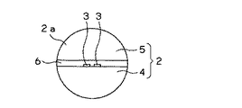
図1に示すように、本発明を適用した光学素子1は、近接場での位相変化を検出可能とするものであり、SIL(Solid Immersion Lens)と呼ばれるレンズ体2にプローブ3が埋め込まれた構造を有している。
As shown in FIG. 1, an
具体的に、このレンズ体2は、高屈折率の光学ガラスからなる球体の一部を平らに削り取り、研磨して形成された半球状のレンズであり、平面側を集光された光ビームの出射面2aとし、球面側を集光された光ビームが入射される入射面2bとしている。さらに、このレンズ体2は、出射面2aと直交する方向、すなわち光軸Aに沿った方向に2分割された第1のレンズ素子4と第2のレンズ素子5とから構成されている。これら第1のレンズ素子4及び第2のレンズ素子5は、球体をその中心を通り且つ互い直交する2平面により4分割されてなる、いわゆる1/4球であり、出射面2aと直交する互いの接合面4a,5aを突き合わせて溶着又は光学接着剤を用いて接着により接合することで、全体略半球状のレンズ体2を構成している。
Specifically, the
プローブ3は、図2及び図3に示すように、金属や、半金属、レンズ体2と異なる屈折率を有する透明導電材等の導体又は誘電体からなる。また、このプローブ3は、第1のレンズ素子4と第2のレンズ素子5との間に配置されるように、互いに接合される第1のレンズ素子4と第2のレンズ素子5との何れか一方の接合面(ここでは、接合面4a)にリソグラフィ技術を用いてパターン形成されている。具体的に、このプローブ3は、レンズ体2の光軸中心において、先端部3aが出射面2aに臨むと共に、光軸方向に長尺且つ微細な形状とされている。
As shown in FIGS. 2 and 3, the
ここで、レンズ体2の出射面2aに臨むプローブ3の先端部3aは、図4及び図5に示すように、このレンズ体2の出射面2aに集光される光ビームのスポットよりも小となる大きさ(幅、厚さ)で形成されている。ここでは、例えば幅が20nm程度、厚さが20nm程度となる大きさで略矩形状に形成されている。
Here, the
なお、SILのような半球レンズの場合、レンズ体2の入射面2bから入射された光ビームは、出射面2aに対して垂直に入射する。このとき、レンズ体2の出射面2bに集光される光ビームのスポットは、1.22×λ/NAで決まる。また、開口数NA=n・sinθ(n:屈折率)である。
In the case of a hemispherical lens such as SIL, the light beam incident from the
また、このプローブ3は、レンズ体2の内部に埋めまれる基端部3b側がレンズ体2の出射面2aに臨む先端部3a側よりも大となる形状を有している。
Further, the
これにより、光学顕微鏡を用いて、レンズ体2に埋め込まれたプローブ3の位置確認を容易に行うことができる。特に、プローブ3の大きさが光学顕微鏡の分解能の限界となる100〜200nm程度以下となった場合には、このプローブ3の先端部3aの位置を光学顕微鏡で確認することは困難であり、このプローブ3の先端部3aとレンズ体2の出射面2aに集光される光ビームのスポットとの位置合わせができなくなる。そこで、プローブ3の基端部3b側を光学顕微鏡の焦点深度の数倍程度の深さから光学顕微鏡の分解能の限界以上の大きさ(幅、厚さ)とすることで、このプローブ3の位置確認が可能となる。
Thereby, the position confirmation of the
なお、プローブ3の基端部3b側は、レンズ体2の入射面2bから入射する光ビームを邪魔しない形状、すなわちレンズ体2に埋め込まれたプローブ3によって光ビームが屈折したり、反射によってレンズ体2の内部で光ビームの軌跡が影響を受けない形状とする必要がある。これにより、レンズ体2の光軸中心から入射した光ビームは、レンズ体2の出射面2bに集光された際に、超解像のスポットを形成することになる。
The
また、プローブ3が形成された第1のレンズ素子4の接合面4a上には、図3に示すように、このプローブ3を保護するための保護層6aと、第1のレンズ素子4と第2のレンズ素子5とを接着するための接着層6bとが形成されている。すなわち、第1のレンズ素子4と第2のレンズ素子5との間には、保護層6a及び接着層6bからなる中間層6が形成されている。保護層6aは、レンズ体2と同一材料からなる光学ガラスや酸化アルミニウム(アルミナ)等からなり、真空成膜法等により数μm程度の厚みで形成されている。接着層6bは、屈折率が光学ガラスと同程度、例えば1.4〜1.5以上となる光学接着剤からなる。
Further, on the joint surface 4a of the
以上のように構成されるレンズ素子1は、レンズ体2に埋め込まれたプローブ3と、光記録媒体100に形成された導電体膜又は誘電体膜との電磁相互作用による光の微弱な位相変化を検出することを基本原理としている。
The
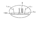
すなわち、この光学素子1を用いて、例えば光ディスク100の凹凸ピットを読み出す場合には、レンズ体2に埋め込まれたプローブ3と光ディスク100の表面にコートされた記録層(例えばCr)とが電磁相互作用を起こす。その作用は、プローブ3の先端部3aと記録層の表面との距離に依存する。このとき、プローブ3の先端部3aに検出光L1を集光すると、集光された検出光L1は、上記電磁相互作用により位相がずれる。これを参照光L2との位相差干渉効果を用いて検出することで、プローブ3の先端部3aの大きさに応じた解像度で信号の読み出しが可能となる。すなわち、集光された検出光L1のスポットS1よりも微少な凹凸ピットを再生することが可能となる。
That is, for example, when the concave and convex pits of the
具体的には、同一光源から出射されたレーザ光を検出光L1と参照光L2とに分岐して光学素子1に入射し、その出射面2aに2つのスポットS1,S2を形成する。そして、検出光L1のスポットS1に対応する位置にプローブ3を配置し、これら検出光L1と参照光L2との光ディスク100からの戻り光の干渉を利用して信号を再生する。
Specifically, the laser light emitted from the same light source is branched into detection light L 1 and reference light L 2 and enters the
ここで、観測される位相差Δφは、数1で表される。すなわち、Siの電気感磁率χは、χ=14.0+14iであり、位相差Δφは、光ディスク100の表面にコートされたCrのχ(=−1.4+37.4i)との積に依存する。
Here, the observed phase difference Δφ is expressed by

したがって、プローブ3は、Cr,Si以外に、Au(χ=0.188+5.39i)やAl(χ=2.80+8.45i)のように、電気感磁率χの虚数部分の大きな導電材料を用いて形成することが好ましい。
Therefore, in addition to Cr and Si, the
次に、本発明を適用した光学素子1の製造方法について説明する。
Next, a method for manufacturing the
上記光学素子1を作製する際は、先ず、図6に示すように、高屈折率を有する光学ガラスからなる第1のガラス基板20を用意する。そして、図7に示すように、この第1のガラス基板20上に、スパッタリング法や、イオンビームデポジション法等の真空成膜法によって、プローブ3となる薄膜21を成膜する。この薄膜21の材料としては、金属や、半金属、レンズ体2と異なる屈折率を有する透明導電材等の導体又は誘電体を用いることができる。ここでは、例えばCrからなる薄膜21を成膜した。また、プローブ3の厚さは、成膜時の膜厚によって決まるが、真空成膜法を用いた場合、膜厚をサブナノメータ精度で制御可能である。したがって、ナノメータ程度の極めて高精度な薄膜21が成膜されることになる。
When producing the
次に、図8に示すように、この薄膜21が成膜された第1のガラス基板20上に、レジスト22を塗布する。
Next, as shown in FIG. 8, a resist 22 is applied on the
次に、図9に示すように、直接電子ビーム描画法(EB描画法)等の電子線リソグラフィ法によって、プローブ3に対応した複数のレジストマスク22aをパターン形成する。このレジストマスク22aは、EB描画法によって10〜20nm程度の幅で高精度にパターン形成することができる。
Next, as shown in FIG. 9, a plurality of resist masks 22a corresponding to the
次に、図10に示すように、このレジストマスク22aを用いて、イオンミリングやリアクティブ・イオン・エッチング法(RIE法)等の真空エッチング法によって、レジストに覆われていない薄膜21を除去する。
Next, as shown in FIG. 10, using this resist mask 22a, the
次に、図11に示すように、第1のガラス基板20上からレジストマスク22aを剥離する。これにより、第1のガラス基板20上には、各光学素子1に対応した同一形状からなる複数のプローブ3がパターン形成されることになる。
Next, as shown in FIG. 11, the resist mask 22 a is peeled off from the
なお、複数のプローブ3が形成された第1のガラス基板20上には、これらプローブ3を保護するための保護層6aが形成される。この保護層6aは、第1のガラス基板20と同一材料からなる光学ガラスや酸化アルミニウム(アルミナ)等からなり、真空成膜法等により数μm程度の厚みで形成される。
A protective layer 6a for protecting the
次に、図12及び図13に示すように、この第1のガラス基板20を複数のプローブ3が長手方向に並ぶ方向に沿って分割する。
Next, as shown in FIGS. 12 and 13, the
次に、図14に示すように、分割された第1のガラス基板20のプローブ3が形成された面に、屈折率が光学ガラスと同程度、例えば1.4〜1.5以上となる光学接着剤を塗布することで接着層6bを形成する。そして、この第1のガラス基板20と、当該第1のガラス基板20と同一材料及び同一形状からなる第2のガラス基板23とを接着する。これにより、第1のガラス基板20と第2のガラス基板21とが互いに突き合わされて接合される接合面の間にプローブ3が位置するように接合一体化されたガラスブロック24が形成される。なお、第1のガラス基板20と第2のガラス基板23との接合方法としては、例えばオプティカルコンタクト法のように、表面粗度が良好な面を圧着し、熱を加えて接合面を溶着する方法を用いることができる。
Next, as shown in FIG. 14, on the surface of the divided
次に、図15に示すように、このガラスブロック24に対して機械的研磨を施すことによって、円柱状のガラスブロック24を形成する。
Next, as shown in FIG. 15, the
次に、図16に示すように、各光学素子1に対応した略半球状の凹部25aが複数並んで形成された砥石25を円柱状のガラスブロック24の外周面に押し当てながら、このガラスブロックを図16中矢印X1方向に回転させる砥石研削加工を行う。これにより、各光学素子1に対応して分割された略球状のレンズ体26が形成される。
Next, as shown in FIG. 16, while pressing the grindstone 25 formed by arranging a plurality of substantially hemispherical concave portions 25 a corresponding to each
次に、図17に示すように、互いに平行に配置された2枚の研磨板27a,27bの間に、球状のレンズ体26を挟み込み、この研磨板27a,27bを図17中に示す矢印X2,X3方向、すなわち互いに逆向きに回転させることで、これら複数のレンズ体26に対して球面研磨加工を行う。
Next, as shown in FIG. 17, a
次に、図18に示すように、球状のレンズ体26を保持具28で保持し、この保持具29を研磨板29に対して図18中矢印X4方向に往復移動させながら、このレンズ体26に対して、接合面と直交する面をプローブ3の先端部が臨む位置まで平坦化する平面研磨加工を行う。これにより、平面研磨加工により平坦化された面を集光された光ビームの出射面2aとする半球状又は超半球状のレンズ体2が形成される。
Next, as shown in FIG. 18, the
ここで、各光学素子1に対応したプローブ3の基端部3b側には、位置決め基準となるマーカ3cが形成されている。球状のレンズ体26は、このマーカ3cによって内部に埋め込まれたプローブ3の位置確認を容易に行うことができ、このマーカ3cを基準にして平面研磨加工を行うことで、レンズ体2の光軸中心にプローブ3の中心を一致させると共に、プローブ3を出射面2aに対して垂直に配置することができる。
Here, a marker 3 c serving as a positioning reference is formed on the
次に、図19に示すように、半球状のレンズ体2に対して仕上げ研磨加工を行う。具体的には、回転台30上に出射面(平面)2aを下面とした状態でレンズ体2を固定し、予め真球度を出したセラミック製の凹型31をレンズ体2の入射面(球面)2bに押し当てながら、レンズ体2を回転台30と一体に図19中矢印X5方向に回転させると共に、凹型31を図19中矢印X6方向に揺動させて研磨加工を行う。これにより、半球状のレンズ体2は、所定の真球度、表面粗度及び収差量を得ることができる。以上のようにして、上記光学素子1を一括して作製することができる。
Next, as shown in FIG. 19, finish polishing is performed on the
次に、本発明を適用した光学素子1の別の構成例について説明する。
Next, another configuration example of the
図20に示す光学素子1は、第1のレンズ素子4と第2のレンズ素子5との間に、複数のプローブ3を光軸と直交する方向に複数並べて配置した構成であり、これら複数のプローブ3は、上記プローブ形成工程において、レジストマスク22aを変更することにより容易にパターン形成することができる。
An
また、図21に示すように、互いに隣接するプローブ3の間隔Tは、レンズ体2の出射面2aに集光される光ビームのスポット径よりも大となることが望ましく、上記検出光L1と上記参照光L2との干渉を防ぐため、2つのスポットS1,S2間の距離よりも大となることが望ましい。
Further, as shown in FIG. 21, the interval T between
光学素子1では、これら複数のプローブ3を光軸と直交する方向に並べて配置することで、検出光L1のスポットS1に対するプローブ3の位置合わせを容易に行うことができる。すなわち、スポットS1とプローブ3の先端部3aとの相対位置は、レンズ加工誤差及びプローブ形成プロセス誤差により位置ずれが生じやすい。そこで、レンズ体2に対する光ビームの入射角を0゜(光軸方向)から僅かに傾けることにより、レンズ体2の出射面2aにおけるスポットの形成位置の調整を行う。また、入射角の調整量が増大すると、スポットの収差が増大したり、実効スポット径が増大し、検出感度の劣化を起こす可能性がある。そこで、プローブ3を光軸と直交する方向に複数並べて配置し、且つ互いに隣接するプローブ3の間隔TをスポットS1,S2間の距離よりも僅かに大きい程度に抑えれば、スポット位置調整量を最大プローブ間隔以内に抑えることが可能となる。
In the
例えば、NAが1.3程度のSILのレンズ体2にプローブ3を埋め込み形成した場合には、スポット径は、およそ0.6μm程度となり、スポット間隔は、SILの直上のウォラストンプリズムの分離角を0.5゜とすると、5μm程度となる。この場合、プローブ間隔Tは、例えば6〜8μm程度とすることが望ましい。
For example, when the
また、複数のプローブ3は、図22及び図23に示すように、第1のレンズ素子4と第2のレンズ素子5との何れか一方の接合面4a,5にリソグラフィ技術によりパターン形成することで、同一面内に複数並べて配置することができる。
In addition, as shown in FIGS. 22 and 23, the plurality of
これに対して、複数のプローブ3は、図24及び図25に示すように、第1のレンズ素子4と第2のレンズ素子5との間に配置された中間層6を介して積層形成する、或いは第1のレンズ素子4の接合面4a及び第2のレンズ素子5の接合面5aにリソグラフィ技術によりパターン形成することで、異なる面内に複数並べて配置することができる。
On the other hand, as shown in FIGS. 24 and 25, the plurality of
また、複数のプローブ3は、形状、寸法、材質のうち少なくとも1つが異なる2種類以上のプローブから構成されたものであってもよい。
Further, the plurality of
この場合、例えば、プローブ3の寸法が異なるものを並べて配置することで、再生時に高分解能モードと低分解能モードとを切り替えるといった使用が可能となる。
In this case, for example, by arranging the
また、上記レンズ素子1では、図26及び図27に示すように、再生用プローブ32と記録用プローブ33とを並べて配置し、再生及び記録を行う構成としてもよい。
Further, as shown in FIGS. 26 and 27, the
このうち、再生用プローブ32は、Si,Au,Ag等の導電体で形成されている。このプローブ32の先端部32aの寸法は、幅20nm程度であり、厚さ20nm程度である。また、プローブ32の幅及び厚さを10nm以下とすることで、更なる高分解能化が可能である。そして、この再生用プローブ32は、検出光L1のスポットS1内に配置されている。
Of these, the reproducing
一方、記録用プローブ33は、Rh等のエレクトロマイグレーションが生じにくい導電体で形成されている。このプローブ33の先端部33aの寸法は、再生用プローブ32と同様に、幅20nm程度であり、厚さ20nm程度である。
On the other hand, the
記録時には、光記録媒体100として誘電体薄膜が形成されたものを用い、記録用プローブ33の先端部33aにパルス電圧を加えることで、ナノ分極ドメインを形成することが可能である。或いは、検出光L1や参照光L2以外の光ビームのスポット内に記録用プローブ33を配置し、ドメイン内の温度を誘電体薄膜のキュリー温度まで上げることにより、抗電界を用いてよりドメインサイズの小さい記録を行うことが可能である。
At the time of recording, a nanopolarized domain can be formed by applying a pulse voltage to the tip 33a of the
また、上記レンズ素子1は、図26及び図27に示すように、上述した単体又は複数のプローブ3に対して電流を流すための電極40を配置した構成であってもよい。
Further, as shown in FIGS. 26 and 27, the
この電極40は、第1のレンズ素子4と第2のレンズ素子5との間に配置されるように、第1のレンズ素子4と第2のレンズ素子5との少なくとも一方の接合面(ここでは、接合面4a)にパターン形成された導体パターン40aからなる。この導体パターン40aは、一端部がプローブ3と電気的に接続されると共に、光軸と略直交する方向に延長された他端部が入射面2aの第1のレンズ素子4と第2のレンズ素子5との間から外部に臨む位置までパターン形成されている。
This
この電極40が形成された光学素子1では、導体パターン40aの他端部が外部配線41aを介して外部電源41と電気的に接続されている。したがって、この電極40からプローブ3に対して、外部電源41のスイッチ41bを切り替えることによって高周波電圧或いは電流変化を印加し、光記録媒体100に形成された導電体膜又は誘電体膜とプローブ3との相互作用を高周波と同期した信号として取り出すことができ、光記録媒体100に記録された信号を高感度に検出し再生することができる。
In the
また、電極40は、図28に示すように、光軸と直交する方向に複数並んで設けられたプローブ3の各基端部3bと1本の導体パターン40aとが電気的に接続された構成であってもよい。この場合、各プローブ3は、全く等価なものとなり、電極40と同電位に接続される。
In addition, as shown in FIG. 28, the
一方、電極40は、図29に示すように、光軸と直交する方向に複数並んで設けられた各プローブ3に対応して複数の導体パターン40aが設けられた構成であってもよい。この場合、各プローブ3は、別個独立に各導体パターン40と接続され、各外部電源41のスイッチ41のオン/オフを切り替えることで、高周波を重畳するプローブ3を選択することが可能である。すなわち、独立した複数のプローブ3が並ぶことで、いわゆるマルチチャンネル再生記録が可能となる。これにより、データレートの向上が可能である。
On the other hand, as shown in FIG. 29, the
ところで、上記光学素子1を用いた信号再生方法では、プローブ3の先端部3aにおいて最小浮上量が得られることがスペーシング制御及び信頼性確保の上で重要となる。特に、ナノメータオーダの再生分解能を得るためには、レンズ体2の出射面2aと光記録媒体100との間の距離(スペーシング)を10〜50nm程度まで近接させる必要がある。しかしながら、レンズ体2が傾いた場合には、このレンズ体2の両側でスペーシングの差が生じてしまい、両者の最小隙間が低下してしまう。したがって、光記録媒体の表面粗さや外部振動の影響等を考慮すると、スペーシングの低下量は、10nm以下に抑える必要がある。
By the way, in the signal reproduction method using the
ここで、レンズ体2の出射面2aの直径を1mmとすると、レンズ体2の両側に発生するスペーシングの差を10nm程度に抑えるには、レンズ体2の傾き(チルト角θ)をθ=tan−1(10nm/1mm)=1×10−4度(゜)まで低減しなければならない。
Here, if the diameter of the exit surface 2a of the
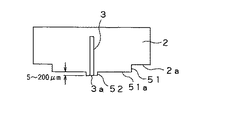
そこで、このような問題を解決するために、レンズ体2の出射面2aには、図30及び図31に示すように、プローブ3の周辺部がパット面51aとして突出された第1の突部51が設けられている。この第1の突部51は、レンズ体2の光軸を中心とした略円柱状の突部であり、パッド面51aの直径をφ10〜100μm程度とし、このパッド面51aの周囲をエッチングすることで、1〜20μm程度の高さで突出形成されている。
Therefore, in order to solve such a problem, as shown in FIGS. 30 and 31, the first projecting portion in which the peripheral portion of the
ここで、図32に示すように、パッド面51aの直径をDとしたとき、姿勢角θにより生じる浮上量の低下量Δhは、Δh=D×tanθとなる。このように、浮上量の低下量Δhは、パッド面51aの直径Dに比例するので、例えば出射面2aの直径が1mm程度のレンズ体2であっても、パッド面51aの直径Dをφ10μm程度とする第1の突部51を出射面2aに突出形成することによって、この浮上量の低下量Δhを1/100程度に低減することができる。
Here, as shown in FIG. 32, when the diameter of the
また、レンズ体2の出射面2aに第1の突部51を設けた場合には、パッド面51aの直径Dの低減に伴い、逆に許容チルト角θは大きくなる。例えば、パッド面51aの直径Dを50μm程度とすると、レンズ体2の両側でのスペーシングの差hを10nm程度に抑えるには、レンズ体2の傾き(許容チルト角θ)は、θ=tan−1(10nm/50μm)=1×10−2度(゜)となる。この角度θは、機械的なチルト角調整で実現できる範囲である。
In addition, when the
さらに、パッド面51aのプローブ3の先端部が臨む中央部には、略円柱状の第2の突部52が突出形成されている。この第2の突部52は、直径がφ1〜10μm程度であり、高さが5〜20nm程度である。このように、プローブ3の近傍を僅かに突出させる第2の突部52を設けることで、プローブ3の先端部3aにおいて最小浮上量が得られることを確実とすることができる。
Furthermore, a substantially cylindrical
次に、上記光学素子1を搭載した光学ヘッドについて説明する。
Next, an optical head equipped with the
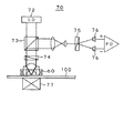
図33に示すように、本発明を適用した光学ヘッド60は、光ビームLを集光させる対物レンズ61と、この対物レンズ61により集光される光ビームLの光路中に配置された上記光学素子1と、これら対物レンズ61及び光学素子1からなる集光レンズを支持する支持体62とを備えている。
As shown in FIG. 33, an
支持体62には、厚み方向に貫通する貫通孔63が設けられており、この貫通孔63には、下面からレンズ体2の出射面2aが臨む上記光学素子1が保持されている。また、支持体62の上面部には、貫通孔62を閉塞するように対物レンズ61が上記光学素子1と光軸を一致させた状態で固定されている。
The
また、支持体62は、浮上スライダを構成しており、この浮上スライダ62が光記録媒体100上を浮上しながら、光記録媒体100に再生光を照射して信号再生を行う。なお、浮上スライダ62と光記録媒体100との間の距離は、10〜50nm程度であり、±1nmの精度で浮上スライダ62が光記録媒体100上を浮上することになる。
Further, the
この光学ヘッド60を作製する際は、先ず、図34に示すように、浮上スライダとなる基板62aを用意し、この基板62aに貫通孔63を設け、この貫通孔63に上記光学素子1を固定する。なお、この基板62aの上下面には、予め所定の平行度を満足するように両面研磨が施されている。また、光学素子1の固定は、エポキシ系接着剤等による接着或いは低融点ガラスによる溶着で行う。
When manufacturing the
次に、光学的に設定された半球高さ又は超半球高さとなるまで、基板62aの下面を研磨する。また、この基板62aの上面に、対物レンズ61を光学的に位置決めした状態で接着する。なお、基板62aの板厚を対物レンズ61の作動距離(ワーキングディスタンス)と一致させるため、この基板61aの上面を研磨してもよい。以上のようして、上記光学ヘッド60を作製することができる。
Next, the lower surface of the substrate 62a is polished until the optically set hemispherical height or super hemispherical height is reached. Further, the
次に、上記光学ヘッド60を用いて、近接場光を利用した光ディスク100に対する信号の再生を行うディスクドライブ装置について説明する。
Next, a disk drive device that uses the
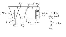
図35に示すように、本発明を適用したディスクドライブ装置70は、光ディスク100を回転駆動する回転駆動手段となるスピンドルモータ71と、このスピンドルモータ71により回転駆動される光ディスク100に対してレーザ光を出射する光源となるレーザダイオード(LD)72と、このレーザダイオード72から出射されたレーザ光の光路中に配されたビームスプリッタ73と、このビームスプリッタ73を透過したレーザ光を検出光L1と参照光L2とに分岐するウォラストンプリズム74と、これら検出光L1及び参照光L2を集光させて光ディスク100の信号記録面に照射する上記光学ヘッド60と、光ディスク100の信号記録面で反射された戻り光をビームスプリッタ73で反射した後に分岐させるウォラストンプリズム75と、このウォラストンプリズムで75分岐されたレーザ光を受光する光強度検出手段となる一対のフォトディテクタ(PD)76とを備えている。
As shown in FIG. 35, a
このディスクドライブ装置70では、スピンドルモータ71により回転駆動される光ディスク100の信号記録面上を浮上スライダ62が浮上しながら、光ディスク100に対する信号の再生が行われる。
In this
具体的に、レーザダイオード72から出射されたレーザ光は、図36に示すように、ビームスプリッタ73と光学ヘッド60の対物レンズ61との間に配置されたウォラストンプリズム74によって僅かな角度で分岐され、一方は検出光L1としてプローブ3の先端部3aに集光され、他方は参照光L2としてプローブ3の先端部3aから外れた位置に集光される。また、光ディスク100の凹凸ピットが形成された信号記録面からの戻り光は、ビームスプリッタ73により反射された後、ウォラストンプリズム5によって分岐されて一対のフォトディテクタ76へと導かれる。
Specifically, the laser light emitted from the
そして、一対のフォトディテクタ76が受光した検出光L1と参照光L2との位相差を干渉測定することにより、光ディスク100からの再生信号が検出される。例えば、プローブ3の先端部3aが光ディスク100のピットの凸部と対向する位置にあるときと、凹部と対向する位置にあるときとで、プローブ3の先端部3aと光ディスク100の記録層との間の距離が変わる。その結果、電磁相互作用の強さが変わり、位相のずれが僅かに変わる。この位相のずれの変化を上記干渉測定により検出し、ピット(信号)を再生する。
Then, a reproduction signal from the
また、上記光学ヘッド60は、図37に示すように、上記浮上スライダ62に代わって、支持体62にヘッド媒体間の距離を測定する測定手段となるセンサ(図示せず)と、このセンサからの測定結果に基づいて、ヘッド媒体間の距離を調整するヘッド駆動手段となるアクチュエータ64とが搭載された構成とすることも可能である。
In addition, as shown in FIG. 37, the
センサとしては、ナノメータオーダで測定可能な静電容量センサ等を用いることができる。アクチュエータ64は、光学ヘッド60を光軸と平行な方向と光軸方向と直交する方向とに、それぞれナノメータオーダで変位駆動するものである。アクチュエータ64としては、例えば光学ピックアップに用いられるボイスコイルモータや、PZT(ピエゾ素子)アクチュエータ等を用いることができる。なお、この光学ヘッド60と光記録媒体100との間の距離は、10〜50nm程度であり、±1nmの精度で光学ヘッド60が光記録媒体100上を走査することになる。
As the sensor, a capacitance sensor or the like that can be measured in nanometer order can be used. The
また、記録及び/又は再生装置では、図38に示すように、このようなアクチュエータ64を搭載する光学ヘッド60を用いる場合、上記ディスクドライブ装置70のスピンドルモータ71に代わって、光記録媒体100が載置されるステージ77aを光記録媒体と平行な面内で互いに直交する2方向に移動させるアクチュエータ77を移動手段として備えた構成とする。なお、このアクチュエータ77には、PZTアクチュエータ、ボイスコイルモータ、ステッピングモータ等を用いることができる。
In the recording and / or reproducing apparatus, as shown in FIG. 38, when an
この場合、光記録媒体100が載置されたステージ77aがアクチュエータ77により面内方向に移動操作されることによって、この光記録媒体100上を光学ヘッド60が走査しながら、光記録媒体100に対する信号の再生が行われる(光学ヘッド60を用いた信号の再生方法については同様であることから、以下説明を省略する。)。
In this case, the stage 77a on which the
また、上記光学ヘッド60は、近接場光を利用した試料の観察を行う近接場光学顕微鏡装置に使用することも可能である。すなわち、この近接場光学顕微鏡装置は、上記ディスクドライブ装置70とほぼ同様の構成及び原理を用いて、試料の表面を光学ヘッド60が走査しながら、レンズ体2に埋め込まれたプローブ3と、試料表面との電磁相互作用による光の微弱な位相変化を検出することで試料の観察を行う。すなわち、同一光源から出射されたレーザ光を検出光L1と参照光L2とに分岐して光学素子1に入射し、その出射面2aに2つのスポットS1,S2を形成する。そして、検出光L1のスポットS1に対応する位置にプローブ3を配置し、これら検出光L1と参照光L2との試料表面からの戻り光の位相差干渉効果を用いて検出することで、プローブ3の先端部3aの大きさに応じた解像度で試料の観察が行われる。
The
以上のように、本発明を適用した光学素子1では、プローブ3のレンズ体2の出射面2aに臨む先端部3aが当該レンズ体2の出射面2aに集光される光ビームのスポットよりも小となることから、当該光ビームのスポットよりも微小なマークを検出することが可能である。具体的には、プローブ3先端部3aの微細化を進めることによって、数〜数10ナノメータオーダのマークを検出することが可能である。
As described above, in the
また、プローブ3は、互いの接合面4a,5aを突き合わせて接合される第1のレンズ素子4と第2のレンズ素子5との何れか一方の接合面4a,5bにパターン形成されることで、この接合面4a,5aと直交する光ビームの出射面2aに臨む当該プローブ3の先端部3aを光軸方向に長尺且つ微細な形状とすることが可能である。
In addition, the
また、プローブ3の微細化は、薄膜形成技術や電子線リソグラフィ技術等を用いることによって、プローブ3の先端部3aの大きさ(幅、厚さ)を数〜数10ナノメータオーダで制御可能なことから、容易且つ再現性よく達成することができる。一方、プローブ3の先端部3aは、幅をナノメータオーダとしたまま、長さを数〜数100μm程度に極めて長く形成することが可能である。
Further, the miniaturization of the
したがって、この光学素子1では、プローブ3の先端部3aの摩耗による影響を受けることなく、高分解能での検出が可能となり、信頼性を大幅に向上させることが可能である。
Therefore, in this
また、本発明を適用した光学素子1の製造方法では、レンズ体2の出射面2aに集光される光ビームのスポットよりも微小なマークを検出し得ると共に、プローブ3の先端部3aの摩耗による影響を受けることなく、高分解能での検出が可能な信頼性の高い上記光学素子1を容易且つ再現性に優れた方法で一括作製することが可能である。
Further, in the method of manufacturing the
また、本発明を適用した光学ヘッド60では、そのような光学素子1を搭載することで、煩雑なサーボ機構が不要となり、近接場光を用いた検出を高感度且つ高速に行うことが可能である。
Further, in the
また、本発明を適用したディスクドライブ装置70等の記録及び/又は再生装置では、そのような光学ヘッド60を用いることで、光記録媒体に対する信号の記録及び/又は再生を高密度に行うことが可能である。
Further, in the recording and / or reproducing apparatus such as the
また、本発明を適用した光学顕微鏡装置では、そのような光学ヘッド60を用いることで、試料に対する観察を高分解能で行うことが可能である。
Further, in the optical microscope apparatus to which the present invention is applied, it is possible to observe the sample with high resolution by using such an
なお、本発明は、上述したSILのような光学素子1に限らず、例えば図39に示すようなSuper−SILと呼ばれる超半球のレンズからなる光学素子や、図40に示すようなSIMと呼ばれる半球レンズ又は超半球レンズに反射膜が形成された光学素子にも適用可能である。
The present invention is not limited to the
また、本発明では、上述した光記録媒体100として、凹凸ピットにより情報が記録されている光ディスクだけでなく、相変化型の光ディスクにおいても、記録マークを検出することが可能である。相変化型の光ディスクでは、例えばGeSbTeなどの相変化材料により形成された信号記録層に対して、光熱記録により、反射率の異なる記録マークが形成される。相変化型の光ディスクにおける反射率の違いは、上記電気感磁率χの違いを意味している。したがって、本発明では、相変化型の光ディスクに形成された微小ピット長の記録マークを検出することが可能である。
In the present invention, the recording mark can be detected not only on the optical disc on which information is recorded by the concave and convex pits but also on the phase change type optical disc as the
同様に、導電体をパーマロイのような高透磁率の材料、または鉄のような強磁性体を用いることによって、光磁気あるいは磁気記録媒体の微少磁区を検出することが可能である。例えば、パーマロイをスライダの下面に配し、これに高周波電流を流し、発生した局部微少磁界が光ディスク上の上向き磁区と下向き磁区とにより、ごく僅か磁界分布に変化を生ずる。この磁界分布の変化は、光との相互作用により光の位相の変化となって検出される。 Similarly, by using a high magnetic permeability material such as permalloy or a ferromagnetic material such as iron as the conductor, it is possible to detect the micromagnetic domain of the magneto-optical or magnetic recording medium. For example, a permalloy is disposed on the lower surface of the slider, a high-frequency current is passed through the slider, and the generated local minute magnetic field causes a slight change in the magnetic field distribution due to the upward magnetic domain and the downward magnetic domain on the optical disk. This change in the magnetic field distribution is detected as a change in the phase of the light due to the interaction with the light.
1 レンズ素子、2 レンズ体、2a 出射面、3 プローブ、3a 先端部、4 第1のレンズ素子、5 第2のレンズ素子、6 中間層、20 第1のガラス基板、23 第2のガラス基板、24 ガラスブロック、40 電極、60 光学ヘッド、70 ディスクドライブ装置、100 光記録媒体
DESCRIPTION OF
Claims (9)
上記複数のプローブが形成された第1の光学ガラスと、この第1の光学ガラスと同質の第2の光学ガラスとを互いに突き合わされて接合される接合面の間に当該プローブが位置するように接合し、接合一体化された光学ガラスブロックを形成するブロック形成工程と、
上記光学ガラスブロックに対して球面研磨加工を施すことによって、各光学素子毎に分割された球状のレンズ体を形成する球面研磨工程と、
上記球状のレンズ体に対して平面研磨加工を施すことによって、接合面と直交する面を上記プローブの先端部が臨む位置まで平坦化し、この面を集光された光ビームの出射面とする半球状又は超半球状のレンズ体を形成する平面研磨工程とを有する光学素子の製造方法。 A probe forming step of patterning a plurality of probes corresponding to each optical element by a lithography technique after forming a film to be a probe on one main surface of the first optical glass;
The first optical glass on which the plurality of probes are formed and the second optical glass of the same quality as the first optical glass are positioned so as to be positioned between the joint surfaces that are brought into contact with each other. A block forming step of bonding and forming an integrated optical glass block;
A spherical polishing step for forming a spherical lens body divided for each optical element by applying a spherical polishing process to the optical glass block;
A hemisphere having a surface that is orthogonal to the bonding surface is flattened to a position where the tip of the probe faces, and that this surface is used as the exit surface of the focused light beam by subjecting the spherical lens body to surface polishing. A method of manufacturing an optical element comprising a planar polishing step of forming a lens body having a shape or a super hemisphere.
光ビームを出射する光源と、
上記光記録媒体に近接した状態で対向配置され、上記光源から出射された光ビームを集光させて上記光記録媒体の信号記録面に照射する光学ヘッドと、
上記光記録媒体の信号記録面で反射された光ビームの光強度の変化を検出する光強度検出手段とを備え、
上記光学ヘッドは、上記光源から出射された光ビームを集光させる対物レンズと、
上記対物レンズにより集光される光ビームの光路中に配置された光学素子と、
上記対物レンズ及び上記光学素子を支持する支持体とを備え、
上記光学素子は、第1のレンズ素子と第2のレンズ素子とが互いの接合面を突き合わせて接合されると共に、この接合面と直交する面を上記対物レンズにより集光された光ビームの出射面とするレンズ体と、
上記第1のレンズ素子と上記第2のレンズ素子との間に配置されると共に、上記レンズ体の出射面に臨む先端部が当該レンズ体の出射面に集光される光ビームのスポットよりも小となるプローブとを備えることを特徴する記録及び/又は再生装置。 In a recording and / or reproducing apparatus for recording and / or reproducing a signal with respect to an optical recording medium using near-field light,
A light source that emits a light beam;
An optical head disposed opposite to the optical recording medium and condensing the light beam emitted from the light source and irradiating the signal recording surface of the optical recording medium;
A light intensity detecting means for detecting a change in light intensity of the light beam reflected by the signal recording surface of the optical recording medium,
The optical head includes an objective lens that collects the light beam emitted from the light source;
An optical element disposed in an optical path of a light beam condensed by the objective lens;
A support for supporting the objective lens and the optical element;
In the optical element, the first lens element and the second lens element are joined by abutting their joint surfaces, and a light beam condensed by the objective lens on a surface orthogonal to the joint surface is emitted. A lens body as a surface;
More than the spot of the light beam that is disposed between the first lens element and the second lens element and that has a leading end facing the exit surface of the lens body that is focused on the exit surface of the lens body. A recording and / or reproducing apparatus comprising a probe that is small.
上記支持体は、上記回転駆動手段により回転駆動される上記光記録媒体の信号記録面上を浮上するスライダであることを特徴とする請求項2記載の記録及び/又は再生装置。 A rotation driving means for rotating the optical recording medium;
3. The recording and / or reproducing apparatus according to claim 2 , wherein the support is a slider that floats on the signal recording surface of the optical recording medium that is rotationally driven by the rotational driving means.
上記測定手段の測定結果に基づいて、上記光学ヘッドを光軸方向に変位駆動するヘッド駆動手段とを備えることを特徴とする請求項2記載の記録及び/又は再生装置。 Measurement means for measuring a distance between the optical recording medium and the optical head based on a change in light intensity detected by the light intensity detection means;
3. The recording and / or reproducing apparatus according to claim 2, further comprising head driving means for driving the optical head to be displaced in the optical axis direction based on the measurement result of the measuring means.
光ビームを出射する光源と、
上記試料と近接した状態で対向配置され、上記光源から出射された光ビームを集光させて上記試料の表面に照射する光学ヘッドと、
上記試料の表面で反射された光ビームの光強度の変化を検出する光強度検出手段とを備え、
上記光学ヘッドは、上記光源から出射された光ビームを集光させる対物レンズと、
上記対物レンズにより集光される光ビームの光路中に配置された光学素子と、
上記対物レンズ及び上記光学素子を支持する支持体とを備え、
上記光学素子は、第1のレンズ素子と第2のレンズ素子とが互いの接合面を突き合わせて接合されると共に、この接合面と直交する面を上記対物レンズにより集光された光ビームの出射面とするレンズ体と、
上記第1のレンズ素子と上記第2のレンズ素子との間に配置されると共に、上記レンズ体の出射面に臨む先端部が当該レンズ体の出射面に集光される光ビームのスポットよりも小となるプローブとを備えることを特徴する光学顕微鏡装置。 In an optical microscope apparatus that observes a sample using near-field light,
A light source that emits a light beam;
An optical head that is arranged opposite to the sample and condenses the light beam emitted from the light source and irradiates the surface of the sample;
A light intensity detecting means for detecting a change in light intensity of the light beam reflected by the surface of the sample,
The optical head includes an objective lens that collects the light beam emitted from the light source;
An optical element disposed in an optical path of a light beam condensed by the objective lens;
A support for supporting the objective lens and the optical element;
In the optical element, the first lens element and the second lens element are joined by abutting their joint surfaces, and a light beam condensed by the objective lens on a surface orthogonal to the joint surface is emitted. A lens body as a surface;
More than the spot of the light beam that is disposed between the first lens element and the second lens element and that has a leading end facing the exit surface of the lens body that is focused on the exit surface of the lens body. An optical microscope apparatus comprising a small probe.
上記支持体は、上記回転駆動手段により回転駆動される上記試料の表面上を浮上するスライダであることを特徴とする請求項6記載の光学顕微鏡装置。 A rotation driving means for rotating the sample;
7. The optical microscope apparatus according to claim 6 , wherein the support is a slider that floats on the surface of the sample that is rotationally driven by the rotational driving means.
上記測定手段の測定結果に基づいて、上記光学ヘッドを光軸方向に変位駆動するヘッド駆動手段とを備えることを特徴とする請求項6記載の光学顕微鏡装置。 Measurement means for measuring a distance between the sample and the optical head based on a change in light intensity detected by the light intensity detection means;
The optical microscope apparatus according to claim 6, further comprising: a head driving unit that drives the optical head to be displaced in the optical axis direction based on a measurement result of the measuring unit.
Priority Applications (1)
| Application Number | Priority Date | Filing Date | Title |
|---|---|---|---|
| JP2003374676A JP4370880B2 (en) | 2003-11-04 | 2003-11-04 | Optical element manufacturing method, recording and / or reproducing apparatus, and optical microscope apparatus |
Applications Claiming Priority (1)
| Application Number | Priority Date | Filing Date | Title |
|---|---|---|---|
| JP2003374676A JP4370880B2 (en) | 2003-11-04 | 2003-11-04 | Optical element manufacturing method, recording and / or reproducing apparatus, and optical microscope apparatus |
Publications (3)
| Publication Number | Publication Date |
|---|---|
| JP2005140853A JP2005140853A (en) | 2005-06-02 |
| JP2005140853A5 JP2005140853A5 (en) | 2006-08-31 |
| JP4370880B2 true JP4370880B2 (en) | 2009-11-25 |
Family
ID=34686320
Family Applications (1)
| Application Number | Title | Priority Date | Filing Date |
|---|---|---|---|
| JP2003374676A Expired - Fee Related JP4370880B2 (en) | 2003-11-04 | 2003-11-04 | Optical element manufacturing method, recording and / or reproducing apparatus, and optical microscope apparatus |
Country Status (1)
| Country | Link |
|---|---|
| JP (1) | JP4370880B2 (en) |
-
2003
- 2003-11-04 JP JP2003374676A patent/JP4370880B2/en not_active Expired - Fee Related
Also Published As
| Publication number | Publication date |
|---|---|
| JP2005140853A (en) | 2005-06-02 |
Similar Documents
| Publication | Publication Date | Title |
|---|---|---|
| US6055220A (en) | Optical disk data storage system with improved solid immersion lens | |
| US7933169B2 (en) | Optical head for near-field recording and reproducing device | |
| JP4060150B2 (en) | Micro-integrated near-field optical recording head and optical recording apparatus using the same | |
| JP2000173093A (en) | Optical element and information recording and reproducing apparatus | |
| JP5028526B2 (en) | Thermally assisted magnetic head and method of assembling the thermally assisted magnetic head | |
| JP3442296B2 (en) | Magneto-optical head device and recording / reproducing device | |
| JP4220153B2 (en) | Recording head, recording head manufacturing method, and information recording apparatus | |
| US7110346B2 (en) | Devices for optical near-files second surface recording | |
| US6762978B2 (en) | Optical head slider, method for manufacturing optical head slider, and recording and/or reproducing apparatus | |
| JP4370880B2 (en) | Optical element manufacturing method, recording and / or reproducing apparatus, and optical microscope apparatus | |
| JP4793323B2 (en) | Manufacturing method of plasmon probe, near-field light generator, optically assisted magnetic recording head, optically assisted magnetic recording device, near-field light microscope device, near-field light exposure device, optical recording device | |
| US6704250B1 (en) | Near-field magneto-optical head having a magnetic sensor | |
| US8284636B2 (en) | Near-field thermally assisted magnetic recording head and recording apparatus thereof | |
| JP2001023230A (en) | Optical head and optical recording and reproducing device | |
| JP2753590B2 (en) | High density memory device | |
| US6934240B2 (en) | Optical element, optical head and signal reproducing method | |
| JP4507840B2 (en) | Optically assisted magnetic recording head, magnetic recording apparatus, and optically assisted magnetic recording head manufacturing method | |
| JP4296924B2 (en) | Exposure apparatus, recording and / or reproducing apparatus | |
| JP2000206126A (en) | Minute cantilever and apparatus utilizing minute force | |
| JP3895458B2 (en) | Near-field optical head | |
| JPH11273126A (en) | Optical recording and reproducing solid immersion lens and optical recording and reproducing device | |
| JP2006286119A (en) | Optical assist type magnetic head, magnetic recorder, and method for manufacturing the optical assist type magnetic head | |
| JPH10172172A (en) | Interval detecting method, interval controller, information recording and reproducing device and recording medium | |
| JP2001174393A (en) | Near-field light device and its manufacture method | |
| JP2000306283A (en) | Method and device for recording/reproducing, and magneto-optical head |
Legal Events
| Date | Code | Title | Description |
|---|---|---|---|
| A521 | Request for written amendment filed |
Free format text: JAPANESE INTERMEDIATE CODE: A523 Effective date: 20060718 |
|
| A621 | Written request for application examination |
Free format text: JAPANESE INTERMEDIATE CODE: A621 Effective date: 20060718 |
|
| A977 | Report on retrieval |
Free format text: JAPANESE INTERMEDIATE CODE: A971007 Effective date: 20081022 |
|
| A131 | Notification of reasons for refusal |
Free format text: JAPANESE INTERMEDIATE CODE: A131 Effective date: 20090519 |
|
| A521 | Request for written amendment filed |
Free format text: JAPANESE INTERMEDIATE CODE: A523 Effective date: 20090714 |
|
| TRDD | Decision of grant or rejection written | ||
| A01 | Written decision to grant a patent or to grant a registration (utility model) |
Free format text: JAPANESE INTERMEDIATE CODE: A01 Effective date: 20090811 |
|
| A01 | Written decision to grant a patent or to grant a registration (utility model) |
Free format text: JAPANESE INTERMEDIATE CODE: A01 |
|
| A61 | First payment of annual fees (during grant procedure) |
Free format text: JAPANESE INTERMEDIATE CODE: A61 Effective date: 20090824 |
|
| FPAY | Renewal fee payment (event date is renewal date of database) |
Free format text: PAYMENT UNTIL: 20120911 Year of fee payment: 3 |
|
| FPAY | Renewal fee payment (event date is renewal date of database) |
Free format text: PAYMENT UNTIL: 20120911 Year of fee payment: 3 |
|
| LAPS | Cancellation because of no payment of annual fees |