JP4363632B2 - Flexible printed circuit board - Google Patents
Flexible printed circuit board Download PDFInfo
- Publication number
- JP4363632B2 JP4363632B2 JP2003385149A JP2003385149A JP4363632B2 JP 4363632 B2 JP4363632 B2 JP 4363632B2 JP 2003385149 A JP2003385149 A JP 2003385149A JP 2003385149 A JP2003385149 A JP 2003385149A JP 4363632 B2 JP4363632 B2 JP 4363632B2
- Authority
- JP
- Japan
- Prior art keywords
- printed circuit
- circuit board
- flexible printed
- printer head
- electric wire
- Prior art date
- Legal status (The legal status is an assumption and is not a legal conclusion. Google has not performed a legal analysis and makes no representation as to the accuracy of the status listed.)
- Expired - Fee Related
Links
Images


Classifications
-
- H—ELECTRICITY
- H05—ELECTRIC TECHNIQUES NOT OTHERWISE PROVIDED FOR
- H05K—PRINTED CIRCUITS; CASINGS OR CONSTRUCTIONAL DETAILS OF ELECTRIC APPARATUS; MANUFACTURE OF ASSEMBLAGES OF ELECTRICAL COMPONENTS
- H05K1/00—Printed circuits
- H05K1/02—Details
- H05K1/0213—Electrical arrangements not otherwise provided for
- H05K1/0216—Reduction of cross-talk, noise or electromagnetic interference
- H05K1/0218—Reduction of cross-talk, noise or electromagnetic interference by printed shielding conductors, ground planes or power plane
- H05K1/0219—Printed shielding conductors for shielding around or between signal conductors, e.g. coplanar or coaxial printed shielding conductors
-
- B—PERFORMING OPERATIONS; TRANSPORTING
- B41—PRINTING; LINING MACHINES; TYPEWRITERS; STAMPS
- B41J—TYPEWRITERS; SELECTIVE PRINTING MECHANISMS, i.e. MECHANISMS PRINTING OTHERWISE THAN FROM A FORME; CORRECTION OF TYPOGRAPHICAL ERRORS
- B41J2/00—Typewriters or selective printing mechanisms characterised by the printing or marking process for which they are designed
- B41J2/005—Typewriters or selective printing mechanisms characterised by the printing or marking process for which they are designed characterised by bringing liquid or particles selectively into contact with a printing material
- B41J2/01—Ink jet
- B41J2/07—Ink jet characterised by jet control
-
- B—PERFORMING OPERATIONS; TRANSPORTING
- B41—PRINTING; LINING MACHINES; TYPEWRITERS; STAMPS
- B41J—TYPEWRITERS; SELECTIVE PRINTING MECHANISMS, i.e. MECHANISMS PRINTING OTHERWISE THAN FROM A FORME; CORRECTION OF TYPOGRAPHICAL ERRORS
- B41J2/00—Typewriters or selective printing mechanisms characterised by the printing or marking process for which they are designed
- B41J2/005—Typewriters or selective printing mechanisms characterised by the printing or marking process for which they are designed characterised by bringing liquid or particles selectively into contact with a printing material
- B41J2/01—Ink jet
- B41J2/135—Nozzles
- B41J2/14—Structure thereof only for on-demand ink jet heads
- B41J2/14016—Structure of bubble jet print heads
- B41J2/14072—Electrical connections, e.g. details on electrodes, connecting the chip to the outside...
-
- B—PERFORMING OPERATIONS; TRANSPORTING
- B41—PRINTING; LINING MACHINES; TYPEWRITERS; STAMPS
- B41J—TYPEWRITERS; SELECTIVE PRINTING MECHANISMS, i.e. MECHANISMS PRINTING OTHERWISE THAN FROM A FORME; CORRECTION OF TYPOGRAPHICAL ERRORS
- B41J2/00—Typewriters or selective printing mechanisms characterised by the printing or marking process for which they are designed
- B41J2/005—Typewriters or selective printing mechanisms characterised by the printing or marking process for which they are designed characterised by bringing liquid or particles selectively into contact with a printing material
- B41J2/01—Ink jet
- B41J2/17—Ink jet characterised by ink handling
- B41J2/175—Ink supply systems ; Circuit parts therefor
- B41J2/17503—Ink cartridges
- B41J2/17526—Electrical contacts to the cartridge
- B41J2/1753—Details of contacts on the cartridge, e.g. protection of contacts
-
- H—ELECTRICITY
- H05—ELECTRIC TECHNIQUES NOT OTHERWISE PROVIDED FOR
- H05K—PRINTED CIRCUITS; CASINGS OR CONSTRUCTIONAL DETAILS OF ELECTRIC APPARATUS; MANUFACTURE OF ASSEMBLAGES OF ELECTRICAL COMPONENTS
- H05K1/00—Printed circuits
- H05K1/02—Details
- H05K1/11—Printed elements for providing electric connections to or between printed circuits
- H05K1/118—Printed elements for providing electric connections to or between printed circuits specially for flexible printed circuits, e.g. using folded portions
-
- H—ELECTRICITY
- H05—ELECTRIC TECHNIQUES NOT OTHERWISE PROVIDED FOR
- H05K—PRINTED CIRCUITS; CASINGS OR CONSTRUCTIONAL DETAILS OF ELECTRIC APPARATUS; MANUFACTURE OF ASSEMBLAGES OF ELECTRICAL COMPONENTS
- H05K2201/00—Indexing scheme relating to printed circuits covered by H05K1/00
- H05K2201/09—Shape and layout
- H05K2201/09209—Shape and layout details of conductors
- H05K2201/09218—Conductive traces
- H05K2201/09236—Parallel layout
Description
本発明は,フレキシブルプリント基板に関し,さらに詳細には,インピーダンスを最小化することによりプリント速度が向上されるプリンタヘッドと連結されるフレキシブルプリント基板に関する。 The present invention relates to a flexible printed circuit board, and more particularly to a flexible printed circuit board connected to a printer head in which a printing speed is improved by minimizing impedance.
インクジェットプリンタあるいはコピー機などの湿式現像方式の印刷機は,インクカートリッジを用いて画像を形成する。インクカートリッジは,印刷機から入力された印刷命令信号,即ち,ヒータ選択信号に応じてインクカートリッジ内に格納されたモノまたはカラーのインクをプリンタヘッドを介して印刷用紙に排出させる。プリンタヘッドは,インクを吐出する基板であってインクカートリッジの一部に形成される。 A wet-development-type printing machine such as an ink jet printer or a copier forms an image using an ink cartridge. The ink cartridge discharges mono or color ink stored in the ink cartridge to the printing paper via the printer head in response to a print command signal input from the printing machine, that is, a heater selection signal. The printer head is a substrate that ejects ink and is formed on a part of the ink cartridge.
このとき,印刷機から入力されたヒータ選択信号をプリンタヘッドに伝達するための装置が必要とされる。かかる装置をフレキシブルプリント基板(Flexible Printed Circuit:以下,FPCという)と称する。即ち,FPC印刷機とプリンタヘッドを電気的に連結する一種の印刷回路基板( Printed Circuit Board:PCB)である。 At this time, a device for transmitting the heater selection signal input from the printing machine to the printer head is required. Such an apparatus is referred to as a flexible printed circuit (hereinafter referred to as FPC). That is, it is a kind of printed circuit board (PCB) that electrically connects the FPC printer and the printer head.
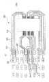
以下,図1に基づいて,印刷機の一例としてインクジェットプリンタを用いて詳説する。図1は,従来のプリンタヘッドと連結されたFPCの一部を概略的に示す平面図である。 Hereinafter, based on FIG. 1, it demonstrates in detail using an inkjet printer as an example of a printing machine. FIG. 1 is a plan view schematically showing a part of an FPC connected to a conventional printer head.
図1に示すように,従来のFPC100は,複数の電圧供給端子110,複数の接地端子120,複数の信号端子130,複数の第1の電線115,及び複数の第2の電線125を有する。さらに,電圧供給端子110はP,接地端子120はG,信号端子130はSに図示される。
As shown in FIG. 1, the conventional FPC 100 includes a plurality of
色相別に駆動される電圧供給端子110は,インクジェットプリンタから受信された印刷命令信号に応じて電圧を供給する。接地端子120は,FPC100を接地させるための端子であって,1つの電圧供給端子110に少なくとも2つの接地端子120が備えられる。信号端子130は,インクジェットプリンタから受信される制御信号に応じて適応的に機能を行なう端子である。
The
第1の電線115は,電圧供給端子110と後述するプリンタヘッド150の第1のボンディングパッド152を電気的に連結する配線である。第1の電線115は,接地端子120と後述するプリンタヘッド150の第2のボンディングパッド154を電気的に連結する配線である。信号端子130とプリンタヘッド150とを連結する配線の図示は省略する。
The first
また,インク吐出のために複数のヒータ(図示せず)を有するプリンタヘッド150はインクカートリッジの一面に備えられ,複数の第1のボンディングパッド152及び第2のボンディングパッド154を有する。その他のプリンタヘッド150に備られるFET素子などの説明及び図面の図示は省略する。
A
複数の第1及び第2のボンディングパッド152,154は,プリンタヘッド150の両側面(即ち,第1の側端及び第2の側端)に分散されて備えられる。アルミニウムからなる第1及び第2のボンディングパッド152,154は,超音波融着によって各々第1及び第2の電線115,125の終端部であるリード(lead)とボンディングされる。
The plurality of first and
インクカートリッジの一面に備えられるプリンタヘッド150は,FPC100によりインクジェットプリンタから受信される印刷命令信号に応じてインクを吐出する。
A
印刷命令信号が受信されれば,電圧供給端子(例えば,Y1−P)110と連結されたヒータ(図示せず)及び少なくとも2つの接地端子(例えば,Y1−G)120に形成されるインピーダンスは抵抗,キャパシタンス及びインダクタンスのうち,インダクタンスからの影響を大きく受ける。即ち,インダクタンス値が大きければインピーダンスは上昇するのである。 When the print command signal is received, the impedance formed in the heater (not shown) connected to the voltage supply terminal (eg, Y1-P) 110 and the at least two ground terminals (eg, Y1-G) 120 is Of resistance, capacitance, and inductance, it is greatly affected by inductance. That is, if the inductance value is large, the impedance increases.
表1は,図1のプリンタヘッドと連結されたFPC100から測定されたインダクタンス値を表す。
Table 1 shows inductance values measured from the

表1及び図1に示すように,Yは黄色,Mはマゼンタ,Cはシアンを具現するグループであり,色相ブロックの第1及び第2は各色相グループ(Y,M,C)がプリンタヘッド150の第1の側端及び第2の側端に連結されることを意味する。さらに,Y1は黄色を具現するために1つの電圧供給端子(Y1−P)及び2つの接地端子(Y1−G)からなり,Y2,M1,M2,C1,及びC2の構成においてはY1と類似しているためその詳説は省略する。
上記のように、プリンタヘッドにヒータ選択信号を伝達するための配線構造を備えたFPCの典型的な例が、特開平7−178910号公報や特表2005−503949号公報に開示されている。
As described above, typical examples of an FPC having a wiring structure for transmitting a heater selection signal to a printer head are disclosed in Japanese Patent Application Laid-Open Nos. 7-178910 and 2005-503949.
しかしながら,図1に示すように,所定のグループ(Y1)から第1の電線115と第2の電線125が所定の距離以上に離間されFPC100に備えられたり,第1及び第2の電線115,125の直径がほぼ同一である場合,従来のFPC100は表1のように高いインダクタンス値を有するようになる。
However, as shown in FIG. 1, the first
さらに,従来のインクジェットプリンタは,プリントの高速化のために10MHz〜100MHzの最大のデータ伝送周波数が必要とされる。即ち,FPC100のインダクタンス値が表1のように高い状態で高周波を用いてプリントを行なうと,インピーダンスが上昇し電流供給が損失される。このことにより,プリンタヘッド150を駆動するFET素子(図示せず)は必要な電流量が供給されないので,ヒータ(図示せず)が発熱されずプリント速度も遅延される,という問題がある。
Furthermore, the conventional ink jet printer requires a maximum data transmission frequency of 10 MHz to 100 MHz in order to increase printing speed. That is, when printing is performed using a high frequency in a state where the inductance value of the FPC 100 is high as shown in Table 1, the impedance increases and current supply is lost. As a result, a necessary amount of current is not supplied to the FET element (not shown) for driving the
したがって,本発明の目的は,基板上に形成されるインピーダンス成分のうちインダクタンス値を減少させることが可能な新規かつ改良されたフレキシブルプリント基板を提供することにある。 Accordingly, an object of the present invention is to provide a new and improved flexible printed circuit board capable of reducing the inductance value of impedance components formed on the circuit board.
上記課題を解決するために,インク吐出のための少なくとも1つのヒータと,少なくとも1つの第1及び第2のボンディングパッドが形成されたプリンタヘッドに連結されプリンタから受信される印刷命令信号に従って前記少なくとも1つのヒータを選択的に駆動するフレキシブルプリント基板であって,前記プリンタから受信される印刷命令信号の有無に従って前記少なくとも1つのヒータに駆動電圧を選択的に供給する少なくとも1つの電圧供給端子と,一端は前記電圧供給端子に,他端は前記第1のボンディングパッドに連結され,前記駆動電圧を前記ヒータに伝達する少なくとも1つの第1の電線と,接地のための少なくとも1つの接地端子と,一端は前記接地端子に,他端は前記第2のボンディングパッドに連結される少なくとも1つの第2の電線と,を含み,前記第2の電線は,前記第2の電線の所定位置で少なくとも2つのポーションに分岐され,前記第1の電線の両側に沿って所定の距離離間され並行されるように備えられる,如く構成される。 In order to solve the above-described problems, the at least one heater for discharging ink and the at least one first and second bonding pads are connected to a printer head formed with the at least one heater according to a print command signal received from a printer. A flexible printed circuit board that selectively drives one heater, at least one voltage supply terminal that selectively supplies a drive voltage to the at least one heater according to the presence or absence of a print command signal received from the printer; One end connected to the voltage supply terminal, the other end connected to the first bonding pad, at least one first electric wire for transmitting the drive voltage to the heater, at least one ground terminal for grounding, One end is connected to the ground terminal, and the other end is connected to the second bonding pad. A second electric wire, and the second electric wire is branched into at least two portions at a predetermined position of the second electric wire, and is separated by a predetermined distance along both sides of the first electric wire. It is configured as prepared.
また,前記第1の電線と前記第1のポーション間の離間距離と,前記第1の電線と前記第2のポーション間の離間距離は,30μm〜300μmの範囲にある,如く構成するのが好ましい。 Further, it is preferable that the separation distance between the first electric wire and the first portion and the separation distance between the first electric wire and the second portion are in the range of 30 μm to 300 μm. .
また,前記少なくとも1つの第1及び第2のボンディングパッドが前記プリンタヘッド基板の第1の側端及び前記第1の側端に対向する第2の側端に所定の比率で分散され備えられた場合,前記第1の側端の第1及び第2のボンディングパッドに連結される第1及び第2の電線間の離間距離は,前記第2の側端の第1及び第2のボンディングパッドに連結された第1及び第2の電線間の離間距離と相違している,如く構成するのが好ましい。 The at least one first and second bonding pads are distributed and provided at a predetermined ratio on a first side end of the printer head substrate and a second side end opposite to the first side end. In this case, the separation distance between the first and second electric wires connected to the first and second bonding pads at the first side end is determined by the first and second bonding pads at the second side end. It is preferable that the distance between the connected first and second electric wires is different from that of the connected first and second electric wires.
本発明においては,接地のための電線がプリンタヘッドに電圧を供給する電線の両側に沿って備えられるので,フレキシブルプリント基板に形成されるインダクタンス値が減少される。したがって,フレキシブルプリント基板に形成される全インピーダンスも減少し,フレキシブルプリント基板は,高周波においても電線の短絡なしに必要な電流をプリンタヘッドに供給されるのでプリント速度を高めることができる。さらに,接地のための電線がプリントヘッドに電圧供給する電線間距離を調整するのでインダクタンス値を調節し印刷品質が向上される。 In the present invention, since the electric wire for grounding is provided along both sides of the electric wire for supplying voltage to the printer head, the inductance value formed on the flexible printed circuit board is reduced. Therefore, the total impedance formed on the flexible printed circuit board is also reduced, and the flexible printed circuit board can supply a necessary current to the printer head without a short circuit of the electric wire even at a high frequency, so that the printing speed can be increased. Furthermore, since the electric wire for grounding adjusts the distance between the electric wires that supply voltage to the print head, the inductance value is adjusted and the printing quality is improved.
以下に添付図面を参照しながら,本発明の好適な実施の形態について詳細に説明する。なお,本明細書及び図面において,実質的に同一の機能構成を有する構成要素については,同一の符号を付することにより重複説明を省略する。
Hereinafter, preferred embodiments of the present invention will be described in detail with reference to the accompanying drawings. In the present specification and drawings, components having substantially the same functional configuration are denoted by the same reference numerals, and redundant description is omitted.
まず,図2に基づいて,本実施形態にかかるフレキシブルプリント基板(FPC)の構成について説明する。なお,図2Aは,本実施形態にかかるプリンタヘッドに連結されるFPCの一部を概略的に示す平面図である。図2Bは,図2AのFPCと連結されるプリンタヘッドを概略的に示す平面図である。 First, based on FIG. 2, the structure of the flexible printed circuit board (FPC) concerning this embodiment is demonstrated. FIG. 2A is a plan view schematically showing a part of the FPC connected to the printer head according to the present embodiment. FIG. 2B is a plan view schematically showing a printer head connected to the FPC of FIG. 2A.
本実施形態にかかるFPCは,印刷機から受信される印刷命令信号(即ち,ヒータ選択信号)をプリンタヘッドに伝達するための基板である。さらに,プリンタヘッドはFPCを介して受信された印刷命令信号に応じて選択的にスイッチング素子であるFET及びヒータを駆動して印刷命令信号に応じるインクを吐出する。印刷機は,例えば,インクジェットプリンタ,コピー機などを例に挙げられるが,以下ではインクジェットプリンタを例に挙げて説明する。 The FPC according to the present embodiment is a substrate for transmitting a print command signal (that is, a heater selection signal) received from the printing machine to the printer head. Further, the printer head selectively drives FETs and heaters as switching elements according to a print command signal received via the FPC, and ejects ink corresponding to the print command signal. Examples of the printing machine include an ink jet printer and a copying machine, but the following description will be given by taking an ink jet printer as an example.
図2A及び図2Bに示すように,本実施形態にかかるFPC200は,複数の電圧供給端子210,複数の接地端子220,複数の信号端子230,複数の第1の電線215,及び複数の第2の電線225を有する。図面にて,電圧供給端子210と連結された第1の電線215は斜線で,接地端子220と連結された第2の電線225は点線で図示される。
As shown in FIGS. 2A and 2B, the FPC 200 according to the present embodiment includes a plurality of
さらに,電圧供給端子210には,P(power),接地端子220にはG(ground),信号端子230にはS(signal)が示されている。例えば,Y2−Pに表示された電圧供給端子210は,黄色のインクを吐出するための印刷命令信号を受信すると,それに対応する電圧を供給するためにプリンタヘッド250の第1側に備えられる。また,Y2−Gに表示された接地端子220は,Y2−Pと所定の黄色いグループを形成して接地させる端子である。
Further, P (power) is indicated for the
第1の電線215は,電圧供給端子210と後述するプリンタヘッド250の第1のボンディングパッド252を電気的に連結する配線である。即ち,第1の電線215は,連結された電圧供給端子210から供給される駆動電圧を第1のボンディング252を介してそれに対応するヒータ256に伝達する。
The first
第2の電線225は,接地端子220とプリンタヘッド250の第2のボンディングパッド254を電気的に連結する配線である。信号端子230とプリンタヘッド250とを連結する配線の図示は省略する。
The second
第1及び第2のボンディングパッド252,254とボンディングされる第1及び第2電線215,225の一端はリードと言う。リードは,銅からなる第1及び第2の電線215,225の露出された表面を例えば金などの材料でコーティング処理したものである。
One ends of the first and second
電圧供給端子210は,インクジェットプリンタから受信される印刷命令信号の有無に応じて図2Bのプリンタヘッド250に形成されたヒータ256に第1の電線215に沿って駆動電圧を選択的に供給する(信号伝送関係は図示せず)。例えば,電圧供給端子(Y1−P)210に印刷命令信号が受信されれば,印刷命令信号が受信された電圧供給端子(Y1−P)210と電気的に連結されたヒータ256のみが印刷命令信号及び電圧供給端子(Y1−P)210に対応する色相のインクが吐出される。
The
接地端子220は,FPC200の接地のための端子であって,1つの電圧供給端子210に少なくとも1つの接地端子220が設けられる。即ち,1つの電圧供給端子210及び1つの接地端子220は色相別グループをなして駆動される。信号端子230はインクジェットプリンタから受信される制御信号に応じて適応的にその機能を行なう。
The
かかる電圧供給端子210,接地端子220,及び信号端子230の一面は,インクジェットプリンタと電気的に接触するため表面がメッキされている。これをディンプルと言う。
One surface of the
図3は,図2Aに備えられた1つの電圧供給端子及び1つの接地端子を示す平面図である。図4は,図3に示す電圧供給端子と第1及び第2の電線の一部を拡大図示した平面図である。 FIG. 3 is a plan view showing one voltage supply terminal and one ground terminal provided in FIG. 2A. 4 is an enlarged plan view showing a part of the voltage supply terminal and the first and second electric wires shown in FIG.
図3及び図4に示すように,接地端子220に連結された第2の電線225は,所定位置(例えば,一点鎖線で図示されたAの位置)において,少なくとも2つに分岐され電圧供給端子210に連結された第1の電線215の両側に沿って並行される。即ち,第2の電線225は,所定位置(A)で少なくとも2つのポーションに分岐された後,分岐された少なくとも2つのポーションは第1の電線215の長さ方向に沿って備えられる。このとき,少なくとも2つのポーションのうち第1のポーションは,第1の電線215の一側に備えられ,少なくとも2つのポーションのうち第2のポーションは,第1の電線215の他側に備えられる。即ち,分岐された少なくとも2つのポーションのうち第1及び第2のポーションは第1の電線215を中心に各々左側及び右側に備えられる。
As shown in FIGS. 3 and 4, the second
このとき,第2の電線225の分岐された少なくとも2つのポーションは,第1の電線215の両側から所定の距離(d)離間されて備えられる。離間距離(d)は,30μm〜500μmであるのが好ましい。
At this time, the branched at least two portions of the second
さらに,第1及び第2の電線215,225のリードは,1つまたは少なくとも2つに分岐されて各々第1及び第2のボンディングパッド252,254にボンディングされることが好ましい。これは,少なくとも2つに分岐されることにより,リードが並列接続されるので,抵抗は減少して,所定の接点(即ち,分岐されたリードのうちいずれかの1つのリード)が短絡される時,残りの接点(分岐されたリードのうち短絡されたリード他の残りのリード)を使用できるからである。このことにより,FPC200の使用期間も延長できる。
Furthermore, the leads of the first and second
図2Bに示すように,プリンタヘッド250は,図2Aの点線で図示されたところに備えられFPC200と電気的に連結される。
As shown in FIG. 2B, the
インク吐出のためのプリントヘッド250は,インクカートリッジの一面に備えられ,複数の第1及び第2のボンディングパッド252,254及び複数のヒータ256を有する。なお,プリンタヘッド250に備えられるFET素子などの説明及び図面で図示は省略する。
The
複数の第1及び第2のボンディングパッド252,254は,プリンタヘッド250の両側端(即ち,第1の側端及び第2の側端)に分散されて備えられる。本実施形態においては,第1の側端は,第2の側端に比べてFPC200と隣接しているところを指す。アルミニウムからなる第1及び第2のボンディングパッド252,254は,超音波融着によって第1及び第2の電線215,225のリードとボンディングされる。
The plurality of first and
複数のヒータ256は,色相別に区分され,連結された電圧供給端子210から駆動電圧が印加されると,インクを吐出する。
The plurality of
FPC200とプリンタヘッド250が結合されたインクカートリッジがディンプルによりインクジェットプリンタ内のプリンタカートリッジに電気的に接触されると,プリンタヘッド250は,FPC200によりインクジェットプリンタから受信された印刷命令信号に応じてインクを吐出する。
When the ink cartridge in which the
インクジェットプリンタから印刷命令信号が受信されると,受信された印刷命令信号の色相に該当するFPC200の電圧供給端子(例えば,Y2−P)10は,少なくとも1つの接地端子(例えば,Y2−G)220とグループ(例えば,Y2)を形成してプリンタヘッド250のヒータ256を駆動する。
When a print command signal is received from the inkjet printer, the voltage supply terminal (for example, Y2-P) 10 of the
グループY1において,Yは黄色のインクを吐出するためのグループであり,1はグループY1が第1及び第2の電線225によってプリンタヘッド250の第1の側端に連結されていることを意味する。
In the group Y1, Y is a group for discharging yellow ink, and 1 means that the group Y1 is connected to the first side end of the
図5は,図2に示すプリンタヘッド250と連結されるFPC200の一部を図示した回路図である。
FIG. 5 is a circuit diagram illustrating a part of the
図5に示すように,FPC200の第1及び第2の電線215,225のリードは,プリンタヘッド250の第1及び第2のボンディングパッド252,254にボンディングされる。このとき,インクジェットプリンタから印刷命令信号が受信されると,RHで示されたヒータ256は,所定の電圧供給端子(VP)210及びFETで図示されたスイッチング素子のONによって加熱される。このことにより,インクは所定のヒータ256を介して吐出され,回路は所定の接地端子(GND)220により接地される。
As shown in FIG. 5, the leads of the first and second
なお,プリンタヘッド250と連結されたFPC200には数式1のようなインピーダンスが形成される
Note that the impedance as shown in Equation 1 is formed in the
上記数式1に示すように,Zはインピーダンス,RはR1〜R4の合成抵抗,LはL1及びL2の合成インダクタンス,Cはキャパシタンス,wは角速度である。インピーダンス(Z)は数式1のように抵抗(R),インダクタ(L),及びキャパシタンス(C)により形成され,インピーダンス(Z)が低いほどFPC200からプリンタヘッド250への信号及び駆動電圧は円滑に供給される。かかるインピーダンス(Z)はデータ伝送周波数に対してインダクタンス(L)の影響を大きく受ける。
As shown in Equation 1, Z is an impedance, R is a combined resistance of R 1 to R 4 , L is a combined inductance of L 1 and L 2 , C is a capacitance, and w is an angular velocity. The impedance (Z) is formed by a resistor (R), an inductor (L), and a capacitance (C) as in Equation 1, and the lower the impedance (Z), the smoother the signal and drive voltage from the
以下に示す表2は,図2示すプリンタヘッド250と連結されるFPC200から測定されたインダクタンス値を示したものである。
Table 2 shown below shows inductance values measured from the
上記表2に示すように,Yは黄色,Mはマゼンタ,Cはシアンを備えるグループであり,色相ブロックの数字第「1」及び「2」は各々プリンタヘッド250の第1の側端及び第2の側端に連結されることを意味する。
As shown in Table 2, Y is a group including yellow, M is magenta, and C is cyan. The numbers “1” and “2” of the hue block are the first side end and the first end of the
さらに,Y1は1つの電圧供給端子(Y1−P)及び1つの接地端子(Y1−G)からなり,Y2は1つの電圧供給端子(Y2−P)及び1つの接地端子(Y2−G)からなる。これは,M1,M2,C1,及びC2においても同様に適用されるのでその詳説は省略する。 Furthermore, Y1 is composed of one voltage supply terminal (Y1-P) and one ground terminal (Y1-G), and Y2 is composed of one voltage supply terminal (Y2-P) and one ground terminal (Y2-G). Become. Since this applies to M1, M2, C1, and C2 as well, detailed description thereof is omitted.
上記表2にで示すインダクタンス値は,第1に,図4に示すように,第1の電線215の直径(A)が第2の電線225の幅(a)の2倍であり,第2に,第1の電線215と第2の電線225間の離間距離(d)が60μm〜100μmである場合に測定された値である。
The inductance values shown in Table 2 are as follows. First, as shown in FIG. 4, the diameter (A) of the first
上記のように設定された場合,FPC200の色相別グループに形成されるインダクタンスの最小値は5.9nHであり,最大値は16.6nHである。かかるインダクタンスは離間距離に比例するので,第1及び第2の電線215,225間の離間距離を縮小させることによりインダクタンス値を減少させ得る。
When set as described above, the minimum value of the inductance formed in the hue-specific group of the
このように複数の第1及び第2の電線215,225に形成されるインピーダンスが減少されることにより,FPC200はプリンタヘッド250の方にFET素子の駆動に必要な電流を円滑に供給し,電圧及び電流の損失が減少されるので,プリント速度は高速になる。
In this way, the impedance formed in the plurality of first and second
なお,上記表2に示すように,同一の色相を具現するグループであっても第1の側端及び第2の側端にて測定されるインダクタンス値は相異なる。これは,第1の側端及び第2の側端と連結される配線の長さが相違しているからである。相異なるインダクタンス値は第1及び第2の電線215,225間の離間距離(d)を調節することにより調節できる。
Note that, as shown in Table 2, the inductance values measured at the first side end and the second side end are different even in groups that implement the same hue. This is because the lengths of the wirings connected to the first side end and the second side end are different. Different inductance values can be adjusted by adjusting the distance (d) between the first and second
なお,本実施形態にかかるFPC200においては,プリンタヘッド250の第1の側端に連結された第1及び第2の電線215,225間の離間距離(d)と第2の側端に連結された第1及び第2の電線215,225間の離間距離は相違しているのが好ましい。
In the
即ち,第1の側端は,第2の側端に比べてFPC200と隣接したところに位置しているので,第1の側端に連結された第1及び第2の電線215,225間の離間距離が第2の側端に連結された第1及び第2の電線215,225間の離間距離より大きくなるように第1及び第2の電線215,225を備える。
That is, since the first side end is located closer to the
換言すると,インダクタンス値が大きい部分の離間距離が短くなるとインダクタンスが減少し,インダクタンス値が小さい部分の離間距離が長くなるとインダクタンス値が増加される。 In other words, the inductance decreases as the separation distance of the portion with the large inductance value decreases, and the inductance value increases as the separation distance of the portion with the small inductance value increases.
上記離間距離の調節によるインダクタンス値の調節は,印刷品質を向上させる。例えば,FPC200がプリンタヘッド250と連結された場合に,インクジェットプリンタから第1の側端及び第2の側端に位置するヒータ256を同時に駆動するという印刷命令信号が印加されると,インダクタンス値を調節して第1の側端及び第2の側端のインピーダンス値を同一にすることにより,第1の側端及び第2の側端に位置するヒータ256を同時に駆動することが可能である。したがって,相違した位置の2つのヒータ256が相異なる色相のインク又は同じ色相のインクを吐出することにより印刷の品質が向上される。
The adjustment of the inductance value by adjusting the separation distance improves the printing quality. For example, when the
一方,本実施形態にかかるFPC200において,多数の第2の電線225を第1の電線215の左側及び右側に備えることもできる。例えば,3つの第2の電線225のうち1つは第1の電線215の左側に沿って備えられ,残りの2つの電線は第1の電線215の右側に沿って備えられることによっても,インダクタンス値を減少させることができる。
On the other hand, in the
接地のための電線がプリンタヘッドに電圧を供給する電線の両側に沿って備えられるので,フレキシブルプリント基板に形成されるインダクタンス値が減少される。したがって,フレキシブルプリント基板に形成される全インピーダンスも減少し,フレキシブルプリント基板は,高周波においても電線の短絡なしに必要な電流をプリンタヘッドに供給されるのでプリント速度を高めることができる。さらに,接地のための電線がプリントヘッドに電圧供給する電線間距離を調整するのでインダクタンス値を調節し印刷品質が向上される。 Since the grounding wire is provided along both sides of the wire for supplying voltage to the printer head, the inductance value formed on the flexible printed circuit board is reduced. Accordingly, the total impedance formed on the flexible printed circuit board is also reduced, and the flexible printed circuit board can supply a necessary current to the printer head without a short circuit of the electric wire even at a high frequency, thereby increasing the printing speed. Furthermore, since the electric wire for grounding adjusts the distance between the electric wires that supply voltage to the print head, the inductance value is adjusted and the printing quality is improved.
以上,添付図面を参照しながら本発明の好適な実施形態について説明したが,本発明は係る例に限定されないことは言うまでもない。当業者であれば,特許請求の範囲に記載された範疇内において,各種の変更例または修正例に想到し得ることは明らかであり,それらについても当然に本発明の技術的範囲に属するものと了解される。 As mentioned above, although preferred embodiment of this invention was described referring an accompanying drawing, it cannot be overemphasized that this invention is not limited to the example which concerns. It will be apparent to those skilled in the art that various changes and modifications can be made within the scope of the claims, and these are of course within the technical scope of the present invention. Understood.
本発明は,フレキシブルプリント基板に適用可能である。 The present invention is applicable to flexible printed circuit boards.
200 FPC
210 電圧供給端子
215 第1の電線
220 接地端子
225 第2の電線
230 信号端子
200 FPC
210
Claims (13)
前記プリンタから受信される印刷命令信号の有無に従って前記少なくとも1つのヒータに駆動電圧を選択的に供給する少なくとも1つの電圧供給端子と,
一端は前記少なくとも1つの電圧供給端子に,他端は第1のボンディングパッドに各々連結され,前記駆動電圧を前記少なくとも1つのヒータに伝達する少なくとも1つの第1の電線と,
少なくとも1つの接地端子と,
一端は前記少なくとも1つの接地端子に,他端は少なくとも1つの第2のボンディングパッドに連結される少なくとも1つの第2の電線と,を含み,
前記少なくとも1つの第2の電線は,所定位置で少なくとも2つのポーションに分岐され,前記少なくとも2つのポーションが前記少なくとも1つの第1の電線の長さ方向に沿って備えられ,前記少なくとも2つのポーションのうち第1のポーションは前記第1の電線の一側に備えられ,前記少なくとも2つのポーションのうち第2のポーションは前記第1の電線の他側に備えられる,
ことを特徴とするフレキシブルプリント基板。 A flexible printed circuit board coupled to a printer head having at least one heater for ink ejection,
At least one voltage supply terminal for selectively supplying a drive voltage to the at least one heater according to the presence or absence of a print command signal received from the printer;
One end connected to the at least one voltage supply terminal, the other end connected to the first bonding pad, and at least one first electric wire for transmitting the driving voltage to the at least one heater;
At least one ground terminal;
One end including at least one ground terminal, and the other end including at least one second electric wire connected to at least one second bonding pad;
The at least one second electric wire is branched into at least two portions at a predetermined position, the at least two portions are provided along a length direction of the at least one first electric wire, and the at least two portions are provided. A first portion is provided on one side of the first electric wire, and a second portion of the at least two portions is provided on the other side of the first electric wire.
A flexible printed circuit board characterized by that.
ことを特徴とする請求項1に記載のフレキシブルプリント基板。 The separation distance between the first electric wire and the first portion and the separation distance between the first electric wire and the second portion are in the range of 30 μm to 300 μm.
The flexible printed circuit board according to claim 1.
ことを特徴とする請求項1に記載のフレキシブルプリント基板。 The at least one first and second bonding pads are distributed and provided at a predetermined ratio on a first side end of a substrate including the printer head and a second side end opposite to the first side end. In this case, the separation distance between the first and second electric wires connected to the first and second bonding pads at the first side end is determined by the first and second bonding pads at the second side end. Different from the separation distance between the first and second electric wires to be connected,
The flexible printed circuit board according to claim 1.
ことを特徴とする請求項1に記載のフレキシブルプリント基板。 The other ends of the at least one first and second electric wires are branched into at least two and connected to the at least one first and second bonding pads, respectively.
The flexible printed circuit board according to claim 1.
前記プリンタヘッドに電圧を供給する複数の電圧連結配線と,
前記プリンタヘッドの接地のための複数の接地連結配線と,を含み,前記複数の電圧連結配線の各々と前記複数の接地連結配線の各々は、色相別にグループをなして構成され,
複数の前記接地連結配線は,前記プリンタヘッドと接続される接地端子部分で各々少なくとも2つに分割し,各々の前記接地連結配線と同一の色相別グループに対応する各々の前記電圧連結配線の両側に沿って並行するように備えられる,
ことを特徴とするフレキシブルプリント基板。 A flexible printed circuit board connected to a printer head,
A plurality of voltage connecting wires for supplying a voltage to the printer head;
A plurality of ground connection wirings for grounding the printer head, each of the plurality of voltage connection wirings and each of the plurality of ground connection wirings are configured in groups according to hue,
The plurality of ground connection wirings are divided into at least two ground terminal portions connected to the printer head, and both sides of each voltage connection wiring corresponding to the same color group as each ground connection wiring. Prepared to run parallel to,
A flexible printed circuit board characterized by that.
ことを特徴とする請求項11に記載のフレキシブルプリント基板。 The impedance formed on the flexible printed circuit board is adjusted by adjusting a predetermined distance between the plurality of ground connection wires and the plurality of voltage connection wires.
The flexible printed circuit board according to claim 11.
Applications Claiming Priority (1)
| Application Number | Priority Date | Filing Date | Title |
|---|---|---|---|
| KR10-2002-0070908A KR100456029B1 (en) | 2002-11-14 | 2002-11-14 | Flexible Printed Circuit |
Publications (3)
| Publication Number | Publication Date |
|---|---|
| JP2004165673A JP2004165673A (en) | 2004-06-10 |
| JP2004165673A5 JP2004165673A5 (en) | 2006-10-19 |
| JP4363632B2 true JP4363632B2 (en) | 2009-11-11 |
Family
ID=32291738
Family Applications (1)
| Application Number | Title | Priority Date | Filing Date |
|---|---|---|---|
| JP2003385149A Expired - Fee Related JP4363632B2 (en) | 2002-11-14 | 2003-11-14 | Flexible printed circuit board |
Country Status (4)
| Country | Link |
|---|---|
| US (1) | US7040739B2 (en) |
| JP (1) | JP4363632B2 (en) |
| KR (1) | KR100456029B1 (en) |
| CN (1) | CN1292905C (en) |
Families Citing this family (9)
| Publication number | Priority date | Publication date | Assignee | Title |
|---|---|---|---|---|
| JP2004215225A (en) * | 2002-12-17 | 2004-07-29 | Sony Corp | Communication system, communication method, and data processing device |
| CN100384629C (en) * | 2004-11-29 | 2008-04-30 | 晶强电子股份有限公司 | Soft circuit board of ink jet printing head and its producing method |
| JP4827439B2 (en) * | 2005-05-25 | 2011-11-30 | キヤノン株式会社 | Inkjet recording head substrate and inkjet recording head using the substrate |
| JP2007055080A (en) * | 2005-08-24 | 2007-03-08 | Fuji Xerox Co Ltd | Droplet ejection device and current control method |
| US7810910B2 (en) * | 2006-06-29 | 2010-10-12 | Eastman Kodak Company | Fluid-ejecting device with simplified connectivity |
| US8991978B2 (en) * | 2010-05-11 | 2015-03-31 | Hewlett-Packard Development Company, L.P. | Ink pen electrical interface |
| JP5441814B2 (en) * | 2010-05-14 | 2014-03-12 | キヤノン株式会社 | Printed wiring board and device provided with printed wiring board |
| JP5817445B2 (en) * | 2010-11-19 | 2015-11-18 | セイコーエプソン株式会社 | Circuit board |
| CN105329000B (en) * | 2015-12-03 | 2017-08-04 | 上海斐讯数据通信技术有限公司 | A kind of PCB printing equipments and method |
Family Cites Families (14)
| Publication number | Priority date | Publication date | Assignee | Title |
|---|---|---|---|---|
| JPS56134775U (en) * | 1980-03-11 | 1981-10-13 | ||
| JPS63205249A (en) * | 1987-02-20 | 1988-08-24 | Konica Corp | Thermal recording head |
| JPH0715106A (en) * | 1993-06-29 | 1995-01-17 | Toshiba Corp | Printed board |
| JP3229472B2 (en) * | 1993-12-22 | 2001-11-19 | キヤノン株式会社 | Ink jet recording head and ink jet recording apparatus |
| JPH088499A (en) * | 1994-06-17 | 1996-01-12 | Mamoru Kadowaki | Printed circuit board structure of distributed constant circuit |
| JPH10200225A (en) * | 1997-01-14 | 1998-07-31 | Mitsubishi Electric Corp | Printed wiring board and method of identifying components mount positions on the same |
| US6227643B1 (en) * | 1997-05-20 | 2001-05-08 | Encad, Inc. | Intelligent printer components and printing system |
| JP4741045B2 (en) * | 1998-03-25 | 2011-08-03 | セイコーエプソン株式会社 | Electric circuit, manufacturing method thereof and electric circuit manufacturing apparatus |
| JP3667134B2 (en) * | 1999-02-03 | 2005-07-06 | 株式会社リコー | Inkjet head |
| JP3778732B2 (en) * | 1999-07-15 | 2006-05-24 | 日本電産サンキョー株式会社 | Circuit connection board and circuit connection device for IC card reader |
| JP2001102696A (en) * | 1999-09-30 | 2001-04-13 | Kyocera Corp | Wiring board and manufacturing method therefor |
| JP3878795B2 (en) * | 2000-05-30 | 2007-02-07 | 京セラ株式会社 | Multilayer wiring board |
| JP3748770B2 (en) * | 2000-12-04 | 2006-02-22 | 株式会社住友金属エレクトロデバイス | Transmission line substrate, high-frequency transmission structure, and high-frequency package including the same |
| US6652072B2 (en) * | 2001-09-28 | 2003-11-25 | Hewlett-Packard Development Company, L.P. | Interconnect circuit |
-
2002
- 2002-11-14 KR KR10-2002-0070908A patent/KR100456029B1/en not_active IP Right Cessation
-
2003
- 2003-11-14 CN CNB2003101222843A patent/CN1292905C/en not_active Expired - Fee Related
- 2003-11-14 US US10/706,953 patent/US7040739B2/en not_active Expired - Fee Related
- 2003-11-14 JP JP2003385149A patent/JP4363632B2/en not_active Expired - Fee Related
Also Published As
| Publication number | Publication date |
|---|---|
| KR20040042956A (en) | 2004-05-22 |
| JP2004165673A (en) | 2004-06-10 |
| KR100456029B1 (en) | 2004-11-08 |
| CN1519120A (en) | 2004-08-11 |
| US20040095437A1 (en) | 2004-05-20 |
| CN1292905C (en) | 2007-01-03 |
| US7040739B2 (en) | 2006-05-09 |
Similar Documents
| Publication | Publication Date | Title |
|---|---|---|
| US8246135B2 (en) | Headchip and head for array type inkjet printer | |
| US8057000B2 (en) | Element substrate, printhead, head cartridge, and printing apparatus | |
| US7810907B2 (en) | Board for inkjet printing head and inkjet printing head using the same | |
| JP4363632B2 (en) | Flexible printed circuit board | |
| US6428145B1 (en) | Wide-array inkjet printhead assembly with internal electrical routing system | |
| US7533955B2 (en) | Recording apparatus having radiator joined to common voltage wire | |
| JP2007008039A (en) | Ink jet head | |
| JP5637731B2 (en) | Liquid ejection head and electric wiring board | |
| JP2008006642A (en) | Recorder | |
| JPH02206579A (en) | Ink jet printer | |
| US7797831B2 (en) | Method for manufacturing recording apparatus | |
| JP4877519B2 (en) | Flexible wiring material | |
| JP6561753B2 (en) | Droplet ejection apparatus, image forming apparatus, and electrical circuit connection method of droplet ejection apparatus | |
| JP4677272B2 (en) | Inkjet recording head | |
| JP2007287417A (en) | Flexible flat-cable, flexible flat-cable connection method, liquid discharge head using flexible flat-cable connection method, and image forming apparatus | |
| US5988796A (en) | Recording head and recording apparatus using such recording head | |
| US7762646B2 (en) | Head substrate, printhead, head cartridge, and printing apparatus using the printhead or head cartridge | |
| JPH0760953A (en) | Ink jet recording head and recorder loaded with the recording head | |
| JP2007076174A (en) | Recording head system | |
| JPH0939284A (en) | Line type thermal printing head | |
| US10040284B2 (en) | Discharge element substrate, printhead, and printing apparatus | |
| JP3241790B2 (en) | Thermal head with connector pins | |
| JP5994539B2 (en) | Liquid ejection device and wiring connection structure | |
| JP2004284112A (en) | Inkjet head unit | |
| JPH07144407A (en) | Recording head |
Legal Events
| Date | Code | Title | Description |
|---|---|---|---|
| A521 | Written amendment |
Free format text: JAPANESE INTERMEDIATE CODE: A523 Effective date: 20060906 |
|
| A131 | Notification of reasons for refusal |
Free format text: JAPANESE INTERMEDIATE CODE: A131 Effective date: 20070227 |
|
| A521 | Written amendment |
Free format text: JAPANESE INTERMEDIATE CODE: A523 Effective date: 20070528 |
|
| A02 | Decision of refusal |
Free format text: JAPANESE INTERMEDIATE CODE: A02 Effective date: 20070626 |
|
| A521 | Written amendment |
Free format text: JAPANESE INTERMEDIATE CODE: A523 Effective date: 20071024 |
|
| A911 | Transfer of reconsideration by examiner before appeal (zenchi) |
Free format text: JAPANESE INTERMEDIATE CODE: A911 Effective date: 20071119 |
|
| A912 | Removal of reconsideration by examiner before appeal (zenchi) |
Free format text: JAPANESE INTERMEDIATE CODE: A912 Effective date: 20071221 |
|
| RD02 | Notification of acceptance of power of attorney |
Free format text: JAPANESE INTERMEDIATE CODE: A7422 Effective date: 20090515 |
|
| RD04 | Notification of resignation of power of attorney |
Free format text: JAPANESE INTERMEDIATE CODE: A7424 Effective date: 20090706 |
|
| RD04 | Notification of resignation of power of attorney |
Free format text: JAPANESE INTERMEDIATE CODE: A7424 Effective date: 20090707 |
|
| A01 | Written decision to grant a patent or to grant a registration (utility model) |
Free format text: JAPANESE INTERMEDIATE CODE: A01 |
|
| A61 | First payment of annual fees (during grant procedure) |
Free format text: JAPANESE INTERMEDIATE CODE: A61 Effective date: 20090817 |
|
| FPAY | Renewal fee payment (event date is renewal date of database) |
Free format text: PAYMENT UNTIL: 20120828 Year of fee payment: 3 |
|
| R150 | Certificate of patent or registration of utility model |
Free format text: JAPANESE INTERMEDIATE CODE: R150 |
|
| FPAY | Renewal fee payment (event date is renewal date of database) |
Free format text: PAYMENT UNTIL: 20130828 Year of fee payment: 4 |
|
| R250 | Receipt of annual fees |
Free format text: JAPANESE INTERMEDIATE CODE: R250 |
|
| LAPS | Cancellation because of no payment of annual fees |