JP4356555B2 - Nitride semiconductor device - Google Patents
Nitride semiconductor device Download PDFInfo
- Publication number
- JP4356555B2 JP4356555B2 JP2004242880A JP2004242880A JP4356555B2 JP 4356555 B2 JP4356555 B2 JP 4356555B2 JP 2004242880 A JP2004242880 A JP 2004242880A JP 2004242880 A JP2004242880 A JP 2004242880A JP 4356555 B2 JP4356555 B2 JP 4356555B2
- Authority
- JP
- Japan
- Prior art keywords
- nitride semiconductor
- layer
- semiconductor layer
- grown
- multilayer film
- Prior art date
- Legal status (The legal status is an assumption and is not a legal conclusion. Google has not performed a legal analysis and makes no representation as to the accuracy of the status listed.)
- Expired - Lifetime
Links
Images
Description
本発明は、発光ダイオード(LED)、レーザダイオード(LD)、太陽電池、光センサー等の発光素子、受光素子、あるいはトランジスタ、パワーデバイス等の電子デバイスに使用される窒化物半導体(例えば、InXAlYGa1−X−YN、0≦X、0≦Y、X+Y≦1)素子に関する。 The present invention relates to a light emitting diode (LED), a laser diode (LD), a light emitting element such as a solar cell or a photosensor, a light receiving element, or a nitride semiconductor (for example, In X ) used in an electronic device such as a transistor or a power device. Al Y Ga 1-XY N, 0 ≦ X, 0 ≦ Y, X + Y ≦ 1).
窒化物半導体は高輝度純緑色発光LED、青色LEDとして、既にフルカラーLEDディスプレイ、交通信号灯、イメージスキャナー光源等の各種光源で実用化されている。これらのLED素子は基本的に、サファイア基板上にGaNよりなるバッファ層と、SiドープGaNよりなるn側コンタクト層と、単一量子井戸構造、若しくは多重量子井戸構造のInGaN層を包含する活性層と、MgドープAlGaNよりなるp側クラッド層と、MgドープGaNよりなるp側コンタクト層とが順に積層された構造を有しており、20mAにおいて、発光波長450nmの青色LEDで5mW、外部量子効率9.1%、520nmの緑色LEDで3mW、外部量子効率6.3%と非常に優れた特性を示す。 Nitride semiconductors have already been put to practical use in various light sources such as full-color LED displays, traffic signal lights, and image scanner light sources as high-luminance pure green light-emitting LEDs and blue LEDs. These LED elements basically include an active layer including a buffer layer made of GaN on a sapphire substrate, an n-side contact layer made of Si-doped GaN, and an InGaN layer having a single quantum well structure or a multiple quantum well structure. And a p-side cladding layer made of Mg-doped AlGaN and a p-side contact layer made of Mg-doped GaN are sequentially stacked, and at 20 mA, a blue LED with an emission wavelength of 450 nm is 5 mW, external quantum efficiency The green LED of 9.1% and 520 nm shows very excellent characteristics of 3 mW and external quantum efficiency of 6.3%.
また、本出願人は窒化物半導体基板の上に、活性層を含む窒化物半導体レーザ素子を作製して、世界で初めて室温での連続発振1万時間以上を達成したことを発表した(ICNS'97 予稿集,October 27-31,1997,P444-446、及びJpn.J.Appl.Phys.Vol.36(1997)pp.L1568-1571、Part2,No.12A,1 December 1997)。 In addition, the present applicant has announced that a nitride semiconductor laser element including an active layer is fabricated on a nitride semiconductor substrate and has achieved continuous oscillation of 10,000 hours or more at room temperature for the first time in the world (ICNS ' 97 Proceedings, October 27-31, 1997, P444-446, and Jpn. J. Appl. Phys. Vol. 36 (1997) pp. L1568-1571, Part 2, No. 12A, 1 December 1997).
このように窒化物半導体発光デバイスにはInGaNよりなる井戸層を有する単一量子井戸構造、若しくは多重量子井戸構造の活性層を有するダブルへテロ構造が採用されている。しかし活性層を多重量子井戸構造とすると、単一量子井戸構造のものに比較して、活性層全体の膜厚が厚いため、縦方向の直列抵抗が高くなり、例えばLED素子ではVf(順方向電圧)が高くなる傾向にある。 As described above, a single quantum well structure having a well layer made of InGaN or a double hetero structure having an active layer having a multiple quantum well structure is employed in the nitride semiconductor light emitting device. However, if the active layer has a multiple quantum well structure, the thickness of the entire active layer is thicker than that of a single quantum well structure, so that the vertical series resistance increases. For example, in an LED element, Vf (forward direction) Voltage) tends to be high.
Vfを低下させる技術とほぼ同じ技術内容として、例えば特開平9−298341号に活性層よりも上にあるp側の光導波層、コンタクト層等をInAlGaN層を含む超格子層とするレーザ素子が記載されている。この技術はp型の窒化物半導体層をInを含む窒化物半導体層を含む超格子構造とすることによって、p層のキャリア濃度を増加させ、レーザ素子の閾値を低減させようとするものである。しかし、現実にはInAlGaNのような4元混晶の窒化物半導体は結晶性が悪く、またInを含む窒化物半導体はp型になりにくいため、実際に素子を作製することは難しい傾向にある。 For example, Japanese Patent Application Laid-Open No. 9-298341 discloses a laser element in which a p-side optical waveguide layer, a contact layer, and the like above the active layer are superlattice layers including an InAlGaN layer. Are listed. In this technique, the p-type nitride semiconductor layer has a superlattice structure including a nitride semiconductor layer containing In, thereby increasing the carrier concentration of the p layer and reducing the threshold value of the laser element. . However, in reality, quaternary mixed crystal nitride semiconductors such as InAlGaN have poor crystallinity, and nitride semiconductors containing In are unlikely to be p-type, so that it is difficult to actually fabricate devices. .
例えば、LED素子を照明用光源、直射日光の当たる屋外ディスプレイ等に使用するためには、Vfが低下した発光効率の高い素子が求められている。またLDの閾値を低下させて長寿命にし、光ピックアップ等の光源に実用化するためには、よりいっそうの改良が必要である。本発明はこのような事情を鑑みて成されたものであって、その目的とするところは、主としてLED、LD等の窒化物半導体素子の出力を向上させると共に、Vf、閾値を低下させて素子の発光効率を向上させることにある。発光効率が向上することにより、ひいては受光素子等の窒化物半導体を用いた他の電子デバイスの効率も向上させることができる。 For example, in order to use an LED element for an illumination light source, an outdoor display that is exposed to direct sunlight, an element having high luminous efficiency with a reduced Vf is required. Furthermore, in order to lower the LD threshold value to extend the life and put it to practical use as a light source such as an optical pickup, further improvement is necessary. The present invention has been made in view of such circumstances, and the object of the present invention is to improve the output of nitride semiconductor elements such as LEDs and LDs, and lower the Vf and threshold values. It is to improve the luminous efficiency. By improving the light emission efficiency, it is possible to improve the efficiency of other electronic devices using a nitride semiconductor such as a light receiving element.
本発明の窒化物半導体素子は、n側の窒化物半導体層と、p側の窒化物半導体層との間に活性層を有する窒化物半導体素子において、前記n側の窒化物半導体層には、活性層に接して、Inを含む第1の窒化物半導体層と、その第1の窒化物半導体層と異なる組成を有する第2の窒化物半導体層とが積層されたn側多層膜層を有し、前記第1の窒化物半導体層、または前記第2の窒化物半導体層の内の少なくとも一方の膜厚が100オングストローム以下であり、 前記p側の窒化物半導体層には、Alを含む第3の窒化物半導体層と、第3の窒化物半導体と異なる組成を有する第4の窒化物半導体層とが積層されてなるp側多層膜層を有し、前記第3の窒化物半導体層、または前記第4の窒化物半導体の層の内の少なくとも一方の膜厚が100オングストローム以下であることを特徴とする。好ましくは第1の窒化物半導体層および第2の窒化物半導体層の両方を100オングストローム以下、さらに好ましくは70オングストローム以下、最も好ましくは50オングストローム以下にする。このように膜厚を薄くすることにより、多層膜層が超格子構造となって、多層膜層の結晶性が良くなるので、出力が向上する傾向にある。なお、活性層は少なくともInを含む窒化物半導体、好ましくはInGaNよりなる井戸層を有する単一量子井戸構造、若しくは多重量子井戸構造とすることが望ましい。
The nitride semiconductor device of the present invention is a nitride semiconductor device having an active layer between an n-side nitride semiconductor layer and a p-side nitride semiconductor layer, wherein the n-side nitride semiconductor layer includes: In contact with the active layer, there is an n-side multilayer film layer in which a first nitride semiconductor layer containing In and a second nitride semiconductor layer having a composition different from that of the first nitride semiconductor layer are stacked. and, wherein the first nitride semiconductor layer, or the at least one of the thickness of the second nitride semiconductor layer is Ri der 100 angstroms, the nitride semiconductor layer of the p-side comprises Al A third nitride semiconductor layer having a p-side multilayer film in which a third nitride semiconductor layer and a fourth nitride semiconductor layer having a composition different from that of the third nitride semiconductor are stacked; Or the film thickness of at least one of the fourth nitride semiconductor layers is 1; And wherein the Der Rukoto following 0 angstroms. Preferably, both the first nitride semiconductor layer and the second nitride semiconductor layer are 100 angstroms or less, more preferably 70 angstroms or less, and most preferably 50 angstroms or less. By reducing the film thickness in this way, the multilayer film layer has a superlattice structure, and the crystallinity of the multilayer film layer is improved, so that the output tends to be improved. The active layer preferably has a single quantum well structure or a multiple quantum well structure having a well layer made of a nitride semiconductor containing at least In, preferably InGaN.
第1の窒化物半導体層はInXGa1−XN(0<X<1)とし、第2の窒化物半導体層はInYGa1−YN(0≦Y<1、Y<X)、好ましくはGaNとすることが最も好ましい。 The first nitride semiconductor layer In X Ga 1-X N and (0 <X <1), the second nitride semiconductor layer In Y Ga 1-Y N ( 0 ≦ Y <1, Y <X) GaN is most preferable.
さらに、前記第1の窒化物半導体層または前記第2の窒化物半導体層の内の少なくとも一方の膜厚が、近接する第1の窒化物半導体層または第2の窒化物半導体層同士で互いに異なることを特徴とする。即ち、第1の窒化物半導体層または第2の窒化物半導体層を複数層積層した多層膜層を形成した場合に、第2の窒化物半導体層(第1の窒化物半導体層)を挟んだ第1の窒化物半導体層(第2の窒化物半導体層)の膜厚が互いに異なることを意味する。 Furthermore, the thickness of at least one of the first nitride semiconductor layer or the second nitride semiconductor layer is different between adjacent first nitride semiconductor layers or second nitride semiconductor layers. It is characterized by that. That is, when a multilayer film layer in which a plurality of first nitride semiconductor layers or second nitride semiconductor layers are stacked is formed, the second nitride semiconductor layer (first nitride semiconductor layer) is sandwiched between them. It means that the film thicknesses of the first nitride semiconductor layer (second nitride semiconductor layer) are different from each other.
さらにまた、前記第1の窒化物半導体層、または前記第2の窒化物半導体層の内の少なくとも一方のIII族元素の組成が、近接する第1の窒化物半導体層または第2の窒化物半導体層の同一III族元素の組成同士で互いに異なることを特徴とする。即ち、第1の窒化物半導体層または第2の窒化物半導体層を複数層積層した多層膜層を形成した場合に、第2の窒化物半導体層(第1の窒化物半導体層)を挟んだ第1の窒化物半導体層(第2の窒化物半導体層)のIII族元素の組成比が互いに異なることを意味する。 Furthermore, the first nitride semiconductor layer or the second nitride semiconductor in which the composition of at least one group III element in the first nitride semiconductor layer or the second nitride semiconductor layer is close to each other. It is characterized in that the compositions of the same group III elements in the layer are different from each other. That is, when a multilayer film layer in which a plurality of first nitride semiconductor layers or second nitride semiconductor layers are stacked is formed, the second nitride semiconductor layer (first nitride semiconductor layer) is sandwiched between them. This means that the composition ratios of group III elements of the first nitride semiconductor layer (second nitride semiconductor layer) are different from each other.
n側多層膜層は活性層と離間して形成されていても良いが、最も好ましくは活性層に接して形成されているようにする。活性層に接して形成する方がより出力が向上しやすい傾向にある。 The n-side multilayer film layer may be formed apart from the active layer, but is most preferably formed in contact with the active layer. The output tends to be improved more easily when it is formed in contact with the active layer.
また、本発明の第1の窒化物半導体層および第2の窒化物半導体層がアンドープであることを特徴とする。アンドープとは意図的に不純物をドープしない状態を指し、例えば隣接する窒化物半導体層から拡散により混入される不純物も本発明ではアンドープという。なお拡散により混入される不純物は層内において不純物濃度に勾配がついていることが多い。 Further, the first nitride semiconductor layer and the second nitride semiconductor layer of the present invention are undoped. Undoped refers to a state where impurities are not intentionally doped. For example, impurities mixed by diffusion from adjacent nitride semiconductor layers are also referred to as undoped in the present invention. Note that impurities mixed by diffusion often have a gradient in impurity concentration in the layer.
第1の窒化物半導体層または第2の窒化物半導体層のいずれか一方に、n型不純物がドープされていてもよい。これは変調ドープと呼ばれるもので、変調ドープすることにより、出力が向上しやすい傾向にある。なおn型不純物としては、Si、Ge、Sn、S等のIV族、VI族元素を好ましく選択し、さらに好ましくはSi、Snを用いる。 Either the first nitride semiconductor layer or the second nitride semiconductor layer may be doped with an n-type impurity. This is called modulation doping, and the output tends to be improved by modulation doping. As n-type impurities, group IV and group VI elements such as Si, Ge, Sn, and S are preferably selected, and Si and Sn are more preferably used.
また、第1の窒化物半導体層および第2の窒化物半導体層の両方にn型不純物がドープされていてもよい。n型不純物をドープする場合、不純物濃度は5×10²¹/cm3以下、好ましくは1×1020/cm3以下に調整する。5×1021/cm3よりも多いと窒化物半導体層の結晶性が悪くなって、逆に出力が低下する傾向にある。これは変調ドープの場合も同様である。 In addition, both the first nitride semiconductor layer and the second nitride semiconductor layer may be doped with n-type impurities. When doping an n-type impurity, the impurity concentration is adjusted to 5 × 10 21 / cm 3 or less, preferably 1 × 10 20 / cm 3 or less. If it exceeds 5 × 10 21 / cm 3, the crystallinity of the nitride semiconductor layer is deteriorated, and the output tends to decrease. The same applies to modulation doping.
さらに本発明の好ましい態様として、第3の窒化物半導体層、および第4の窒化物半導体層の両方を100オングストローム以下、さらに好ましくは70オングストローム以下、最も好ましくは50オングストローム以下にする。このように膜厚を薄くすることにより、多層膜層が超格子構造となって、多層膜層の結晶性が良くなるので、出力が向上する傾向にある。
Further as a preferred embodiment of the present invention, the third nitride semiconductor layer, and a fourth 100 angstroms or less both nitride semiconductor layer, more preferably 70 angstroms or less, and most preferably below 50 Angstroms. By reducing the film thickness in this way, the multilayer film layer has a superlattice structure, and the crystallinity of the multilayer film layer is improved, so that the output tends to be improved.
第3の窒化物半導体層はAlaGa1−aN(0<a≦1)とし、前記第4の窒化物半導体層はInbGa1−bN(0≦b<1、b<a)、好ましくはGaNとする。 The third nitride semiconductor layer is Al a Ga 1-a N (0 <a ≦ 1), and the fourth nitride semiconductor layer is In b Ga 1-b N (0 ≦ b <1, b <a ), Preferably GaN.
さらに、前記第3の窒化物半導体層、または前記第4の窒化物半導体層の内の少なくとも一方の膜厚が、近接する第3の窒化物半導体層または第4の窒化物半導体層同士で互いに異なることを特徴とする。即ち、第3の窒化物半導体層または第2の窒化物半導体層を複数層積層した多層膜層を形成した場合に、第3の窒化物半導体層(第4の窒化物半導体層)を挟んだ第4の窒化物半導体層(第3の窒化物半導体層)の膜厚が互いに異なることを意味する。 Furthermore, the thickness of at least one of the third nitride semiconductor layer or the fourth nitride semiconductor layer is equal to each other between the adjacent third nitride semiconductor layers or the fourth nitride semiconductor layers. It is characterized by being different. That is, when a multilayer film layer in which a plurality of third nitride semiconductor layers or second nitride semiconductor layers are stacked is formed, the third nitride semiconductor layer (fourth nitride semiconductor layer) is sandwiched. This means that the fourth nitride semiconductor layers (third nitride semiconductor layers) have different film thicknesses.
さらにまた、前記第3の窒化物半導体層、または前記第4の窒化物半導体層の内の少なくとも一方のIII族元素の組成が、近接する第3の窒化物半導体層または第4の窒化物半導体層の同一III族元素の組成同士で互いに異なることを特徴とする。即ち、第3の窒化物半導体層または第4の窒化物半導体層を複数層積層した多層膜層を形成した場合に、第3の窒化物半導体層(第4の窒化物半導体層)を挟んだ第4の窒化物半導体層(第3の窒化物半導体層)のIII族元素の組成比が互いに異なることを意味する。 Furthermore, the third nitride semiconductor layer or the fourth nitride semiconductor in which the composition of the group III element of at least one of the third nitride semiconductor layer or the fourth nitride semiconductor layer is close to each other. It is characterized in that the compositions of the same group III elements in the layer are different from each other. That is, when a multilayer film layer in which a plurality of third nitride semiconductor layers or fourth nitride semiconductor layers are stacked is formed, the third nitride semiconductor layer (fourth nitride semiconductor layer) is sandwiched between them. It means that the composition ratio of the group III elements of the fourth nitride semiconductor layer (third nitride semiconductor layer) is different from each other.
p側多層膜層は、n側多層膜層と同じく活性層と離間して形成されていても良いが、最も好ましくは活性層に接して形成されているようにする。活性層に接して形成する方がより出力が向上しやすい傾向にある。 The p-side multilayer film layer may be formed apart from the active layer in the same manner as the n-side multilayer film layer, but is most preferably formed in contact with the active layer. The output tends to be improved more easily when it is formed in contact with the active layer.
また、本発明の第3の窒化物半導体層および第4の窒化物半導体層がアンドープであることを特徴とする。p側の多層膜層をアンドープとする場合、その膜厚は0.1μm以下にすることが望ましい。0.1μmよりも厚いと、活性層に正孔が注入されにくくなって、出力が低下しやすい傾向にある。なお、アンドープの定義についてはn側多層膜層と同じであるので省略する。 Further, the third nitride semiconductor layer and the fourth nitride semiconductor layer of the present invention are undoped. When the p-side multilayer film is undoped, the film thickness is preferably 0.1 μm or less. If it is thicker than 0.1 μm, it is difficult for holes to be injected into the active layer, and the output tends to decrease. Note that the definition of undoped is the same as that of the n-side multilayer film, and is omitted.
さらに第3の窒化物半導体層または第4の窒化物半導体層のいずれか一方に、p型不純物がドープされていてもよい。変調ドープすることにより、出力が向上しやすい傾向にある。なおp型不純物としては、Mg、Zn、Cd、Be、Ca等のII族元素を好ましく選択し、好ましくは、Mg、Beを用いる。 Furthermore, p-type impurities may be doped in either the third nitride semiconductor layer or the fourth nitride semiconductor layer. By modulation doping, the output tends to be improved. As the p-type impurity, a Group II element such as Mg, Zn, Cd, Be, and Ca is preferably selected, and Mg and Be are preferably used.
また第3の窒化物半導体層および第4の窒化物半導体層の両方にp型不純物がドープされていてもよい。p型不純物をドープする場合、不純物濃度は1×10²²/cm3以下、好ましくは5×1020/cm3以下に調整する。1×1022/cm3よりも多いと窒化物半導体層の結晶性が悪くなって、出力が低下する傾向にある。これは変調ドープの場合も同様である。 Further, both the third nitride semiconductor layer and the fourth nitride semiconductor layer may be doped with p-type impurities. When doping a p-type impurity, the impurity concentration is adjusted to 1 × 10 22 / cm 3 or less, preferably 5 × 10 20 / cm 3 or less. If it exceeds 1 × 10 22 / cm 3, the crystallinity of the nitride semiconductor layer is deteriorated and the output tends to be lowered. The same applies to modulation doping.
以上説明したように、本発明の窒化物半導体素子によると活性層の下にInを含む窒化物半導体層を有するn側多層膜層を有しているため、このn側の多層膜層が何らかの作用を行い、発光素子の出力を向上させる。そのため、低電流で従来のLED素子と同等の出力が得られる。これについては活性層の結晶性を向上させることによるためと推察されるが詳しいことは不明である。LED素子の発光出力が向上するということは、同時にレーザ素子、SLD等の他の発光素子にも同様の作用がある。さらに、本発明は受光素子、太陽電池等、窒化物半導体を用いたあらゆる電子デバイスに適用可能である。 As described above, according to the nitride semiconductor device of the present invention, the n-side multilayer film layer having the nitride semiconductor layer containing In under the active layer is provided. It operates to improve the output of the light emitting element. Therefore, an output equivalent to the conventional LED element can be obtained at a low current. This is presumed to be due to improving the crystallinity of the active layer, but the details are unknown. The improvement in the light emission output of the LED element has the same effect on other light emitting elements such as a laser element and an SLD at the same time. Furthermore, the present invention is applicable to any electronic device using a nitride semiconductor, such as a light receiving element or a solar cell.
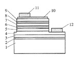
図1は本発明の一実施例に係るLED素子の構造を示す模式的な断面図である。このLED素子はサファイア基板1の上に、GaNよりなる第1のバッファ層2、アンドープGaNよりなる第2のバッファ層3、SiドープGaNよりなるn側コンタクト層4、アンドープGaN層よりなる第3のバッファ層5、InGaN/GaN超格子構造よりなるn側多層膜層6、InGaN/GaNよりなる多重量子井戸構造の活性層7、AlGaN/GaN超格子構造よりなるp側多層膜層8、MgドープGaNよりなるp側コンタクト層9が順に積層された構造を有する。
FIG. 1 is a schematic cross-sectional view showing the structure of an LED element according to an embodiment of the present invention. This LED element has a first buffer layer 2 made of GaN, a second buffer layer 3 made of undoped GaN, an n-
本発明の窒化物半導体素子では、図1に示すように、活性層7を挟んで下部にあるn側窒化物半導体層に、Inを含む第1の窒化物半導体層と、その第1の窒化物半導体層と異なる組成を有する第2の窒化物半導体層とが積層されたn側多層膜層6を有している。n側多層膜層において、第1の窒化物半導体層、第2の窒化物半導体層はそれぞれ少なくとも一層以上形成し、合計で3層以上、さらに好ましくはそれぞれ少なくとも2層以上積層し、合計で4層以上積層することが望ましい。n側多層膜層が活性層に接して形成されている場合、活性層の最初の層(井戸層、若しくは障壁層)と接する多層膜層は第1の窒化物半導体層でも、第2の窒化物半導体層いずれでも良く、n側多層膜層の積層順序は特に問うものではない。なお、図1ではn側多層膜層6が、活性層7に接して形成されているが、この多層膜層と活性層との間に、他のn型窒化物半導体よりなる層を有していても良い。このn側多層膜層を構成する第1の窒化物半導体層または第2の窒化物半導体層の少なくとも一方の膜厚を100オングストローム以下、好ましくは70オングストローム以下、最も好ましくは50オングストローム以下とすることにより、薄膜層が弾性臨界膜厚以下となって結晶が良くなり、その上に積層する第1、若しくは第2の窒化物半導体層の結晶性が良くなり、多層膜層全体の結晶性が良くなるため、素子の出力が向上する。
In the nitride semiconductor device of the present invention, as shown in FIG. 1, a first nitride semiconductor layer containing In is formed on the n-side nitride semiconductor layer below the
第1の窒化物半導体層はInを含む窒化物半導体、好ましくは3元混晶のInXGa1−XN(0<X<1)とし、さらに好ましくはX値が0.5以下のInXGa1−XN、最も好ましくはX値が0.1以下のInXGa1−XNとする。一方、第2の窒化物半導体層は第1の窒化物半導体層と組成が異なる窒化物半導体であれば良く、特に限定しないが、結晶性の良い第2の窒化物半導体を成長させるためには、第1の窒化物半導体よりもバンドギャップエネルギーが大きい2元混晶あるいは3元混晶の窒化物半導体を成長させ、その中でもGaNとすると、全体に結晶性の良い多層膜層が成長できる。従って最も好ましい組み合わせとしては、第1の窒化物半導体層がX値が0.5以下のInXGa1−XNであり、第2の窒化物半導体層がGaNとの組み合わせである。 The first nitride semiconductor layer is a nitride semiconductor containing In, preferably a ternary mixed crystal In X Ga 1-X N (0 <X <1), and more preferably an In value with an X value of 0.5 or less. X Ga 1-X N, most preferably In X Ga 1-X N having an X value of 0.1 or less. On the other hand, the second nitride semiconductor layer may be a nitride semiconductor having a composition different from that of the first nitride semiconductor layer, and is not particularly limited. In order to grow the second nitride semiconductor having good crystallinity, When a binary mixed crystal or a ternary mixed crystal nitride semiconductor having a band gap energy larger than that of the first nitride semiconductor is grown, and GaN among them is grown, a multilayer film layer having good crystallinity can be grown as a whole. Therefore, as the most preferable combination, the first nitride semiconductor layer is In X Ga 1-X N having an X value of 0.5 or less, and the second nitride semiconductor layer is a combination with GaN.
好ましい態様として、第1および第2の窒化物半導体層の膜厚を100オングストローム以下、好ましくは70オングストローム以下、最も好ましくは50オングストローム以下にする。単一窒化物半導体層の膜厚を100オングストローム以下とすることにより、窒化物半導体単一層の弾性臨界膜厚以下となり、厚膜で成長させる場合に比較して結晶性の良い窒化物半導体が成長できる。また、両方を70オングストローム以下にすることによって、多層膜層が超格子構造となり、この結晶性の良い超格子構造の上に活性層を成長させると、多層膜層がバッファ層のような作用をして、活性層が結晶性よく成長できる。 In a preferred embodiment, the thickness of the first and second nitride semiconductor layers is 100 angstroms or less, preferably 70 angstroms or less, and most preferably 50 angstroms or less. By setting the film thickness of the single nitride semiconductor layer to 100 angstroms or less, the nitride semiconductor single layer has an elastic critical film thickness or less, and a nitride semiconductor with better crystallinity is grown as compared with the case of growing with a thick film. it can. Also, by setting both to 70 angstroms or less, the multilayer film layer has a superlattice structure. When an active layer is grown on this superlattice structure with good crystallinity, the multilayer film layer acts like a buffer layer. Thus, the active layer can be grown with good crystallinity.
さらにまた、第1、または前記第2の窒化物半導体層の内の少なくとも一方の膜厚を、近接する第1、または第2の窒化物半導体層同士で互いに異なるようにすることも好ましい。例えば第1の窒化物半導体層をInGaNとし、第2の窒化物半導体層をGaNとした場合、GaN層とGaN層との間のInGaN層の膜厚を、活性層に接近するに従って次第に厚くしたり、また薄くしたりすることにより、多層膜層内部において屈折率が変化するため、実質的に屈折率が次第に変化する層を形成することができる。即ち、実質的に組成傾斜した窒化物半導体層を形成するのと同じ効果が得られる。このため例えばレーザ素子のような光導波路を必要とする素子においては、この多層膜層で導波路を形成して、レーザ光のモードを調整できる。 Furthermore, it is also preferable that the film thickness of at least one of the first or second nitride semiconductor layers is different between adjacent first or second nitride semiconductor layers. For example, when the first nitride semiconductor layer is InGaN and the second nitride semiconductor layer is GaN, the thickness of the InGaN layer between the GaN layer and the GaN layer is gradually increased as it approaches the active layer. Since the refractive index changes inside the multilayer film layer by thinning or reducing the thickness, a layer in which the refractive index gradually changes can be formed. That is, the same effect as that of forming a nitride semiconductor layer having a substantially composition gradient can be obtained. For this reason, in an element that requires an optical waveguide, such as a laser element, the mode of the laser beam can be adjusted by forming a waveguide with this multilayer film layer.
また、第1、または前記第2の窒化物半導体層の内の少なくとも一方のIII族元素の組成を、近接する第1または第2の窒化物半導体層の同一III族元素の組成同士で互いに異なるようにすることも望ましい。例えば、第1の窒化物半導体層をInGaNとし、第2の窒化物半導体層をGaNとした場合、GaN層とGaN層との間のInGaN層のIn組成を活性層に接近するに従って次第に多くしたり、また少なくしたりすることにより、前述の態様と同じく、多層膜層内部において屈折率を変化させて、実質的に組成傾斜した窒化物半導体層を形成することができる。なおIn組成が減少するに従い、屈折率は小さくなる傾向にある。 Further, the composition of at least one group III element in the first or second nitride semiconductor layer is different from each other in the composition of the same group III element in the adjacent first or second nitride semiconductor layer. It is also desirable to do so. For example, when the first nitride semiconductor layer is InGaN and the second nitride semiconductor layer is GaN, the In composition of the InGaN layer between the GaN layer and the GaN layer is gradually increased as it approaches the active layer. By reducing or decreasing the number, the refractive index can be changed inside the multilayer film layer to form a nitride semiconductor layer having a substantially composition gradient, as in the above-described embodiment. The refractive index tends to decrease as the In composition decreases.
第1および第2の窒化物半導体層は両方ともアンドープでも良いし、両方にn型不純物がドープされていても良いし、またいずれか一方に不純物がドープされていてもよい。結晶性を良くするためには、アンドープが最も好ましく、次に変調ドープ、その次に両方ドープの順である。なお両方にn型不純物をドープする場合、第1の窒化物半導体層のn型不純物濃度と、第2の窒化物半導体層のn型不純物濃度は異なっていても良い。 Both the first and second nitride semiconductor layers may be undoped, both may be doped with n-type impurities, or one of them may be doped with impurities. In order to improve crystallinity, undoped is most preferable, followed by modulation doping and then both doping. When both are doped with n-type impurities, the n-type impurity concentration of the first nitride semiconductor layer and the n-type impurity concentration of the second nitride semiconductor layer may be different.
さらに本発明の態様では、p側窒化物半導体層側に、図1に示すように、活性層7を挟んで上部にあるp側窒化物半導体層に、Alを含む第3の窒化物半導体層と、その第3の窒化物半導体層と異なる組成を有する第4の窒化物半導体層とが積層されたp側多層膜層8を有している。p側多層膜層8において、n側の多層膜層6と同様に第3の窒化物半導体層、第4の窒化物半導体層それぞれ少なくとも一層以上形成し、合計で3層以上、さらに好ましくはそれぞれ少なくとも2層以上積層し、合計で4層以上積層することが望ましい。さらに、p側にも多層膜層を設ける場合、n側の多層膜層よりも膜厚を薄くする方が、素子のVf、閾値が低下しやすくなる傾向にある。p側多層膜層が活性層に接して形成されている場合、活性層の最終層(井戸層、若しくは障壁層)と接するp側多層膜層は第3の窒化物半導体層でも、第4の窒化物半導体層いずれでも良い。なお、図1ではp側多層膜層8が、活性層7に接して形成されているが、この多層膜層8と活性層7との間に、他の窒化物半導体よりなる層を有していても良い。
Furthermore, in the aspect of the present invention, as shown in FIG. 1, the p-side nitride semiconductor layer on the p-side nitride semiconductor layer is located on the p-side nitride semiconductor layer, and the third nitride semiconductor layer containing Al And a p-side
さらにまた、第3、または第4の窒化物半導体層の内の少なくとも一方の膜厚を、近接する第3、または第4の窒化物半導体層同士で互いに異なるようにすることも好ましい。例えば第3の窒化物半導体層をAlGaNとし、第4の窒化物半導体層をGaNとした場合、GaN層とGaN層との間のAlGaN層の膜厚を、活性層に接近するに従って次第に厚くしたり、また薄くしたりすることにより、多層膜層内部において屈折率を変化させることができるため、実質的に屈折率が次第に変化する層を形成することができる。即ち、実質的に組成傾斜した窒化物半導体層を形成するのと同じ効果が得られる。このため例えばレーザ素子のような光導波路、光閉じ込め層を必要とする素子においては、この多層膜層で導波路、閉じ込め層を兼用して、レーザ光のモードを調整できる。 Furthermore, it is also preferable that the film thickness of at least one of the third or fourth nitride semiconductor layers be different between adjacent third or fourth nitride semiconductor layers. For example, when the third nitride semiconductor layer is made of AlGaN and the fourth nitride semiconductor layer is made of GaN, the thickness of the AlGaN layer between the GaN layer and the GaN layer is gradually increased as it approaches the active layer. Since the refractive index can be changed inside the multilayer film layer by making it thinner or thinner, a layer in which the refractive index gradually changes can be formed. That is, the same effect as that of forming a nitride semiconductor layer having a substantially composition gradient can be obtained. For this reason, for example, in an element such as a laser element that requires an optical waveguide and an optical confinement layer, the mode of laser light can be adjusted by using this multilayer film layer also as the waveguide and confinement layer.
また、第3、または第4の窒化物半導体層の内の少なくとも一方のIII族元素の組成を、近接する第3、または第4の窒化物半導体層の同一III族元素の組成同士で互いに異なるようにすることも望ましい。例えば、第1の窒化物半導体層をAlGaNとし、第2の窒化物半導体層をGaNとした場合、GaN層とGaN層との間のAlGaN層のAl組成を活性層に接近するに従って次第に多くしたり、また少なくしたりすることにより、前述の態様と同じく、多層膜層内部において屈折率を変化させて、実質的に組成傾斜した窒化物半導体層を形成することができる。なおAl組成が増加するに従い、屈折率は小さくなる。従って目的に応じて、これら組成傾斜した層をp層側に配することができる。 Further, the composition of at least one group III element in the third or fourth nitride semiconductor layer is different from each other in the composition of the same group III element in the adjacent third or fourth nitride semiconductor layer. It is also desirable to do so. For example, when the first nitride semiconductor layer is made of AlGaN and the second nitride semiconductor layer is made of GaN, the Al composition of the AlGaN layer between the GaN layer and the GaN layer is gradually increased as it approaches the active layer. By reducing or decreasing the number, the refractive index can be changed inside the multilayer film layer to form a nitride semiconductor layer having a substantially composition gradient, as in the above-described embodiment. The refractive index decreases as the Al composition increases. Therefore, depending on the purpose, these composition-graded layers can be arranged on the p-layer side.
第3の窒化物半導体層はAlを含む窒化物半導体、好ましくは3元混晶のAlaGa1−aN(0<a<1)とし、最も好ましくはa値が0.5以下のAlaGa1−aNとする。0.5を超えると結晶性が悪くなってクラックが入りやすい傾向にある。一方、第4の窒化物半導体層は第3の窒化物半導体層と組成が異なる窒化物半導体であれば良く、特に限定しないが、結晶性の良い第4の窒化物半導体を成長させるためには、第1の窒化物半導体よりもバンドギャップエネルギーが小さい2元混晶あるいは3元混晶の窒化物半導体を成長させ、その中でもGaNとすると、全体に結晶性の良い多層膜層が成長できる。従って最も好ましい組み合わせとしては、第3の窒化物半導体層がa値が0.5以下のAlaGa1−aNであり、第4の窒化物半導体層がGaNとの組み合わせである。 The third nitride semiconductor layer is a nitride semiconductor containing Al, preferably ternary mixed crystal Al a Ga 1-a N (0 <a <1), and most preferably an Al value of 0.5 or less. It is set as aGa1 - aN. If it exceeds 0.5, the crystallinity is poor and cracks tend to occur. On the other hand, the fourth nitride semiconductor layer may be a nitride semiconductor having a composition different from that of the third nitride semiconductor layer, and is not particularly limited. In order to grow the fourth nitride semiconductor having good crystallinity, When a binary mixed crystal or a ternary mixed crystal nitride semiconductor having a band gap energy smaller than that of the first nitride semiconductor is grown, and GaN among them is grown, a multilayer film having good crystallinity can be grown as a whole. Therefore, as the most preferable combination, the third nitride semiconductor layer is Al a Ga 1-a N having an a value of 0.5 or less, and the fourth nitride semiconductor layer is a combination with GaN.
さらに、第3の窒化物半導体層の膜厚を100オングストローム以下、好ましくは70オングストローム以下、最も好ましくは50オングストローム以下にする。同様に第4の窒化物半導体層の膜厚も100オングストローム以下、好ましくは70オングストローム以下、最も好ましくは50オングストローム以下とする。このように単一窒化物半導体層の膜厚を100オングストローム以下とすることにより、窒化物半導体の弾性臨界膜厚以下となり、厚膜で成長させる場合に比較して結晶性の良い窒化物半導体が成長でき、また窒化物半導体層の結晶性が良くなるので、p型不純物を添加した場合にキャリア濃度が大きく抵抗率の小さいp層が得られ、素子のVf、閾値等が低下しやすい傾向にある。 Further, the thickness of the third nitride semiconductor layer is set to 100 angstroms or less, preferably 70 angstroms or less, and most preferably 50 angstroms or less. Similarly, the thickness of the fourth nitride semiconductor layer is 100 angstroms or less, preferably 70 angstroms or less, and most preferably 50 angstroms or less. Thus, by setting the film thickness of the single nitride semiconductor layer to 100 angstroms or less, the nitride semiconductor becomes less than the critical critical film thickness of the nitride semiconductor, and a nitride semiconductor having better crystallinity than the case of growing with a thick film can be obtained. Since the nitride semiconductor layer can be grown and the crystallinity of the nitride semiconductor layer is improved, a p-layer having a large carrier concentration and a low resistivity can be obtained when a p-type impurity is added, and the Vf, threshold value, etc. of the device tend to decrease. is there.
第3の窒化物半導体層および第4の窒化物半導体層は両方ともアンドープでも良いし、両方にp型不純物がドープされていても良いし、またいずれか一方にp型不純物がドープされていてもよい。キャリア濃度の高いp層を得るには、変調ドープが最も好ましい。なお、先にも述べたようにアンドープとした場合にはその膜厚は0.1μm以下、好ましくは700オングストローム以下、さらに好ましくは500オングストローム以下にする。0.1μmを超えると、アンドープ層の抵抗値が高くなる傾向にあるからである。両方にp型不純物をドープする場合、第3の窒化物半導体層のp型不純物濃度と、第4の窒化物半導体層のp型不純物濃度は異なっていても良い。
実施例1.
図1を元に実施例1について説明する。
Both the third nitride semiconductor layer and the fourth nitride semiconductor layer may be undoped, or both may be doped with a p-type impurity, or one of them may be doped with a p-type impurity. Also good. In order to obtain a p-layer having a high carrier concentration, modulation doping is most preferable. As described above, when undoped, the film thickness is 0.1 μm or less, preferably 700 angstroms or less, more preferably 500 angstroms or less. This is because when the thickness exceeds 0.1 μm, the resistance value of the undoped layer tends to increase. When both are doped with p-type impurities, the p-type impurity concentration of the third nitride semiconductor layer may be different from the p-type impurity concentration of the fourth nitride semiconductor layer.
Example 1.
A first embodiment will be described with reference to FIG.
サファイア(C面)よりなる基板1をMOVPEの反応容器内にセットし、水素を流しながら、基板の温度を1050℃まで上昇させ、基板のクリーニングを行う。基板1にはサファイアC面の他、R面、A面を主面とするサファイア、その他、スピネル(MgA12O4)のような絶縁性の基板の他、SiC(6H、4H、3Cを含む)、Si、ZnO、GaAs、GaN等の半導体基板を用いることができる。
The
(第1のバッファ層2)
続いて、温度を510℃まで下げ、キャリアガスに水素、原料ガスにアンモニアとTMG(トリメチルガリウム)とを用い、基板1上にGaNよりなるバッファ層2を約200オングストロームの膜厚で成長させる。なおこの低温で成長させる第1のバッファ層2は基板の種類、成長方法等によっては省略できる。
(First buffer layer 2)
Subsequently, the temperature is lowered to 510 ° C., hydrogen is used as a carrier gas, ammonia and TMG (trimethyl gallium) are used as a source gas, and a buffer layer 2 made of GaN is grown on the
(第2のバッファ層3)
バッファ層2成長後、TMGのみ止めて、温度を1050℃まで上昇させる。1050℃になったら、同じく原料ガスにTMG、アンモニアガスを用い、アンドープGaNよりなる第2のバッファ層3を1μmの膜厚で成長させる。第2のバッファ層は先に成長させた第1のバッファ層よりも高温、例えば900℃〜1100℃で成長させ、InXAlYGa1−X−YN(0≦X、0≦Y、X+Y≦1)で構成でき、その組成は特に問うものではないが、好ましくはGaN、X値が0.2以下のAlXGa1−XNとすると結晶欠陥の少ない窒化物半導体層が得られやすい。また膜厚は特に問うものではなく、バッファ層よりも厚膜で成長させ、通常0.1μm以上の膜厚で成長させる。
(Second buffer layer 3)
After the growth of the buffer layer 2, only TMG is stopped and the temperature is raised to 1050 ° C. When the temperature reaches 1050 ° C., the second buffer layer 3 made of undoped GaN is grown to a thickness of 1 μm using TMG and ammonia gas as source gases. The second buffer layer is grown at a higher temperature than the first buffer layer grown earlier, for example, 900 ° C. to 1100 ° C., and In X Al Y Ga 1- XYN (0 ≦ X, 0 ≦ Y, X + Y ≦ 1), and the composition thereof is not particularly limited. However, when GaN and Al X Ga 1-X N having an X value of 0.2 or less are used, a nitride semiconductor layer with few crystal defects can be obtained. Cheap. The film thickness is not particularly limited, and the film is grown thicker than the buffer layer, and is usually grown to a thickness of 0.1 μm or more.
(n側コンタクト層4)
続いて1050℃で、同じく原料ガスにTMG、アンモニアガス、不純物ガスにシランガスを用い、Siを3×10¹⁹/cm3ドープしたGaNよりなるn側コンタクト層を3μmの膜厚で成長させる。このn側コンタクト層4も第2のバッファ層3と同様に、InXAlYGa1−X−YN(0≦X、0≦Y、X+Y≦1)で構成でき、その組成は特に問うものではないが、好ましくはGaN、X値が0.2以下のAlXGa1−XNとすると結晶欠陥の少ない窒化物半導体層が得られやすい。膜厚は特に問うものではないが、n電極を形成する層であるので1μm以上の膜厚で成長させることが望ましい。さらにn型不純物濃度は窒化物半導体の結晶性を悪くしない程度に高濃度にドープすることが望ましく、1×1018/cm3以上、5×1021/cm3以下の範囲でドープすることが望ましい。
(N-side contact layer 4)
Subsequently, at 1050 ° C., an n-side contact layer made of GaN doped with Si at 3 × 10 19 / cm 3 is grown to a thickness of 3 μm using TMG as the source gas and silane gas as the impurity gas. Similar to the n-
(第3のバッファ層5)
次にシランガスのみを止め、1050℃で同様にしてアンドープGaNよりなる第3のバッファ層5を100オングストロームの膜厚で成長させる。この第3のバッファ層5もInXAlYGa1−X−YN(0≦X、0≦Y、X+Y≦1)で構成でき、その組成は特に問うものではないが、好ましくはGaN、X値が0.2以下のAlXGa1−XN、またはY値が0.1以下のInYGa1−YNとすると結晶欠陥の少ない窒化物半導体層が得られやすい。このアンドープGaN層を成長させることにより、高濃度で不純物をドープしたn側コンタクト層4の上に直接活性層を成長させるのと異なり、下地の結晶性が良くなるため、次に成長させる窒化物半導体を成長しやすくする。このように、アンドープの窒化物半導体層よりなる第2のバッファ層3の上に、高濃度でn型不純物をドープした窒化物半導体よりなるn側コンタクト層4、次にアンドープの窒化物半導体(n側多層膜層も含む。)よりなる第3のバッファ層5を積層した3層構造とすると、LED素子にした場合にVfが低下しやすい傾向にある。なおn側多層膜層6をアンドープにする場合は第3のバッファ層5を省略することができる。
(Third buffer layer 5)
Next, only the silane gas is stopped, and a third buffer layer 5 made of undoped GaN is grown to a thickness of 100 Å in the same manner at 1050 ° C. The third buffer layer 5 also In X Al Y Ga 1-X -Y N (0 ≦ X, 0 ≦ Y, X + Y ≦ 1) can be configured in its composition but is not intended asks particularly preferably GaN, When Al X Ga 1-X N having an X value of 0.2 or less or In Y Ga 1-Y N having a Y value of 0.1 or less, a nitride semiconductor layer with few crystal defects is easily obtained. By growing this undoped GaN layer, the crystallinity of the underlying layer is improved unlike the case where the active layer is grown directly on the n-
(n側多層膜層6)
次に、温度を800℃にして、TMG、TMI、アンモニアを用い、アンドープIn0.03Ga0.97Nよりなる第1の窒化物半導体層を25オングストローム成長させ、続いて温度を上昇させ、その上にGaNよりなる第2の窒化物半導体層を25オングストローム成長させる。そしてこれらの操作を繰り返し、第1+第2の順で交互に10層づつ積層した超格子構造よりなるn側多層膜を500オングストロームの膜厚で成長させる。
(N-side multilayer film layer 6)
Next, the temperature is set to 800 ° C., and the first nitride semiconductor layer made of undoped In 0.03 Ga 0.97 N is grown by 25 Å using TMG, TMI, and ammonia, and then the temperature is increased. A second nitride semiconductor layer made of GaN is grown thereon by 25 angstroms. These operations are repeated, and an n-side multilayer film having a superlattice structure in which 10 layers are alternately laminated in the first + second order is grown to a thickness of 500 angstroms.
(活性層7)
次に、アンドープGaNよりなる障壁層を200オングストロームの膜厚で成長させ、続いて温度を800℃にして、TMG、TMI、アンモニアを用いアンドープIn0.4Ga0.6Nよりなる井戸層を30オングストロームの膜厚で成長させる。そして障壁+井戸+障壁+井戸・・・・+障壁の順で障壁層を5層、井戸層4層交互に積層して、総膜厚1120オングストロームの多重量子井戸構造よりなる活性層7を成長させる。活性層7は障壁層から積層したが、積層順は井戸層から積層して、井戸層で終わってもよく、また井戸層から積層して障壁層で終わる場合、障壁層から積層して井戸層で終わっても良く積層順は特に問わない。井戸層の膜厚としては100オングストローム以下、好ましくは70オングストローム以下、さらに好ましくは50オングストローム以下に調整する。100オングストロームよりも厚いと、出力が向上しにくい傾向にある。一方、障壁層の厚さは300オングストローム以下、好ましくは250オングストローム以下、最も好ましくは200オングストローム以下に調整する。
(Active layer 7)
Next, a barrier layer made of undoped GaN is grown to a thickness of 200 angstroms, followed by a temperature of 800 ° C., and a well layer made of undoped In 0.4 Ga 0.6 N using TMG, TMI, and ammonia. Growing with a film thickness of 30 Å. Then, five barrier layers and four well layers are alternately stacked in the order of barrier + well + barrier + well. Let The
(p側多層膜層8)
次に、TMG、TMA、アンモニア、Cp2Mg(シクロペンタジエニルマグネシウム)を用い、Mgを5×10¹⁹/cm3ドープしたp型Al0.05Ga0.95Nよりなる第3の窒化物半導体層を25オングストロームの膜厚で成長させ、続いてCp2Mg、TMAを止めアンドープGaNよりなる第4の窒化物半導体層を25オングストロームの膜厚で成長させる。そしてこれらの操作を繰り返し、第3+第4の順で交互に4層ずつ積層した超格子よりなるp側多層膜層8を200オングストロームの膜厚で成長させる。
(P-side multilayer film layer 8)
Next, a third nitridation made of p-type Al 0.05 Ga 0.95 N doped with 5 × 10 19 / cm 3 of Mg using TMG, TMA, ammonia, Cp 2 Mg (cyclopentadienyl magnesium) The physical semiconductor layer is grown to a thickness of 25 angstroms, and then Cp 2 Mg and TMA are stopped, and a fourth nitride semiconductor layer made of undoped GaN is grown to a thickness of 25 angstroms. Then, these operations are repeated, and the p-
(p側コンタクト層9)
続いて1050℃で、TMG、アンモニア、Cp2Mgを用い、Mgを1×10²⁰/cm3ドープしたp型GaNよりなるp側コンタクト層8を700オングストロームの膜厚で成長させる。p側コンタクト層8もInXAlYGa1−X−YN(0≦X、0≦Y、X+Y≦1)で構成でき、その組成は特に問うものではないが、好ましくはGaNとすると結晶欠陥の少ない窒化物半導体層が得られやすく、またp電極材料と好ましいオーミック接触が得られやすい。
(P-side contact layer 9)
Subsequently, at 1050 ° C., a p-
反応終了後、温度を室温まで下げ、さらに窒素雰囲気中、ウェーハを反応容器内において、700℃でアニーリングを行い、p型層をさらに低抵抗化する。 After the completion of the reaction, the temperature is lowered to room temperature, and the wafer is annealed in a reaction vessel at 700 ° C. in a nitrogen atmosphere to further reduce the resistance of the p-type layer.
アニーリング後、ウェーハを反応容器から取り出し、最上層のp側コンタクト層9の表面に所定の形状のマスクを形成し、RIE(反応性イオンエッチング)装置でp側コンタクト層側からエッチングを行い、図1に示すようにn側コンタクト層4の表面を露出させる。
After annealing, the wafer is taken out from the reaction vessel, a mask having a predetermined shape is formed on the surface of the uppermost p-side contact layer 9, and etching is performed from the p-side contact layer side with an RIE (reactive ion etching) apparatus. As shown in FIG. 1, the surface of the n-
エッチング後、最上層にあるp側コンタクト層のほぼ全面に膜厚200オングストロームのNiとAuを含む透光性のp電極10と、そのp電極10の上にボンディング用のAuよりなるpパッド電極11を0.5μmの膜厚で形成する。一方、エッチングにより露出させたn側コンタクト層4の表面にはWとAlを含むn電極12を形成してLED素子とした。
After etching, a translucent p-
このLED素子は順方向電圧20mAにおいて、520nmの純緑色発光を示し、Vfは3.2Vしかなく、従来の多重量子井戸構造のLED素子に比較して、Vfで0.8V近く低下し、出力は2倍以上に向上した。そのため、10mAで従来のLED素子とほぼ同等の特性を有するLEDが得られた。 This LED element emits pure green light of 520 nm at a forward voltage of 20 mA, Vf is only 3.2 V, and Vf is nearly 0.8 V lower than that of a conventional multi-quantum well structure LED element. Improved more than twice. For this reason, an LED having substantially the same characteristics as a conventional LED element at 10 mA was obtained.
本実施例において、n側多層膜層を構成する第2の窒化物半導体層はGaNで構成したが、他のInXAlYGa1−X−YN(0≦X、0≦Y、X+Y≦1)、好ましくはIn組成が第1の窒化物半導体よりも小さいInGaNで構成することもできる。またp側多層膜層を構成する第4の窒化物半導体層はGaNで構成したが、他のInXAlYGa1−X−YN(0≦X、0≦Y、X+Y≦1)、好ましくは第3の窒化物半導体よりもAl組成の小さいAlGaNで構成することもできる。 In the present example, the second nitride semiconductor layer constituting the n-side multilayer film layer is composed of GaN, but other In X Al Y Ga 1-XY N (0 ≦ X, 0 ≦ Y, X + Y ≦ 1), Preferably, the In composition may be made of InGaN smaller than that of the first nitride semiconductor. The fourth nitride semiconductor layer constituting the p-side multi-film layer is constituted with GaN, other In X Al Y Ga 1-X -Y N (0 ≦ X, 0 ≦ Y, X + Y ≦ 1), Preferably, it may be made of AlGaN having an Al composition smaller than that of the third nitride semiconductor.
なお、従来のLED素子の構成は、GaNよりなる第1のバッファ層の上に、アンドープGaNよりなる第2のバッファ層、SiドープGaNよりなるn側コンタクト層、実施例1と同一の多重量子井戸構造よりなる活性層、単一のMgドープAl0.1Ga0.9N層、MgドープGaNからなるp側コンタクト層を順に積層したものである。 The configuration of the conventional LED element is the same as in Example 1, except that the second buffer layer made of undoped GaN, the n-side contact layer made of Si-doped GaN, and the first quantum layer made of GaN. An active layer having a well structure, a single Mg-doped Al 0.1 Ga 0.9 N layer, and a p-side contact layer made of Mg-doped GaN are sequentially stacked.
実施例2.
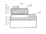
図2は実施例2に係るLED素子の構造を示す模式断面図である。このLED素子は、実施例1において、第3のバッファ層5を成長させず、さらにp側多層膜層8を超格子構造とせずに、Mgを5×10¹⁹/cm3ドープしたp型Al0.1Ga0.9N層よりなるp側クラッド層8’を200オングストロームの膜厚で成長させる他は、同様にしてLED素子を作製したところ、同じく20mAにおいて、Vfは3.3Vと非常に良好な値を示し、出力も1.8倍以上に向上した。
Example 2
FIG. 2 is a schematic cross-sectional view illustrating the structure of the LED element according to the second embodiment. This LED element is a p-type Al doped with 5 × 10 19 / cm 3 Mg in Example 1 without growing the third buffer layer 5 and without forming the p-side
実施例3.
実施例1において、n側多層膜層6を成長する際に、第2の窒化物半導体層のみを、Siを1×10¹⁸/cm3ドープしたGaNとする。また、p側多層膜層を超格子構造とせずに、Mgを5×1019/cm3ドープしたp型Al0.1Ga0.9N層よりなるp側クラッド層8’を200オングストロームで成長させる他は同様にして、LED素子を作製したところ、実施例2とほぼ同等の特性を有するLED素子が得られた。
Example 3
In Example 1, when the n-side
実施例4.
実施例1において、n側多層膜層6を成長する際に、第1の窒化物半導体層をSiを1×10¹⁸/cm3ドープしたIn0.03Ga0.97層とし、第2の窒化物半導体層を、Siを5×1018/cm3ドープしたGaNとする。また、p側多層膜層を超格子構造とせずに、Mgを5×1019/cm3ドープしたp型Al0.1Ga0.9N層よりなるp側クラッド層8’とする他は同様にして、LED素子を作製したところ、20mAにおいてVfは3.4V、出力は従来のものに比較して、1.5倍以上と優れた特性を示した。
Example 4
In Example 1, when the n-side
実施例5.
実施例1において、第3のバッファ層5を成長させず、さらにp側多層膜層8を成長する際に、第4の窒化物半導体層にMgを1×10¹⁹/cm3ドープしたp型GaN層を成長させる他は同様にしてLED素子を作製したところ、実施例1とほぼ同等の特性を有するLED素子が得られた。
Embodiment 5 FIG.
In Example 1, when the third buffer layer 5 is not grown and the p-side
実施例6.
実施例1において、第3のバッファ層5を成長させず、さらにp側多層膜層8を成長する際に、アンドープAl0.05Ga0.95Nよりなる第3の窒化物半導体層を25オングストロームと、アンドープGaNよりなる第4の窒化物半導体層を25オングストロームとでそれぞれ2層づつ交互に積層して総膜厚100オングストロームとする他は同様にしてLED素子を作製したところ、実施例4とほぼ同等の特性を有するLED素子が得られた。
Example 6
In Example 1, when the third buffer layer 5 is not grown and the p-side
実施例7.
実施例1において、n側多層膜層6を成長させる際、アンドープIn0.03Ga0.97Nよりなる第1の窒化物半導体層を50オングストローム成長させ、次にアンドープGaNよりなる第2の窒化物半導体層を25オングストローム成長させる。続いてアンドープIn0.03Ga0.97N層を45オングストローム成長させ、続いてアンドープGaN層を25オングストローム成長させ、次にアンドープIn0.03Ga0.97N層を40オングストローム成長させる。このようにして第1の窒化物半導体層のみを5オングストロームずつ薄くして、5オングストロームまで成長させ、第1の層と第2の層とを交互に10層づつ積層した超格子構造よりなるn側多層膜を合計525オングストロームの膜厚で成長させる。
Example 7
In Example 1, when the n-side
一方、同じく実施例1において、p側多層膜層8を成長させる際、Mgを5×10¹⁹/cm3ドープしたp型Al0.05Ga0.95Nよりなる第3の窒化物半導体層を40オングストロームの膜厚で成長させ、次にアンドープGaNよりなる第4の窒化物半導体層を25オングストロームの膜厚で成長させ、次にMgを同量ドープしたp型Al0.05Ga0.95N層を35オングストローム、次にアンドープGaNを25オングストローム成長させる。このようにして第3の窒化物半導体層のみを5オングストロームずつ薄くして、20オングストロームまで成長させ、第3の層と、第4の層とを交互に5層づつ積層した超格子構造よりなるp側多層膜を合計275オングストロームの膜厚で成長させる。
On the other hand, in Example 1, when the p-side
その他は実施例1と同様にしてLED素子を得たところ、実施例1のものとほぼ同等の特性を有する素子が得られた。なお、本実施例において、n側多層膜6を構成する第1の窒化物半導体層のみの膜厚を変えていったが、第2の窒化物半導体層の膜厚を変えても同様の効果が得られる。またp側多層膜8を構成する第3の窒化物半導体層のみの膜厚を変えていったが、第4の窒化物半導体層の膜厚を変えても同様の効果が得られる。
Otherwise, an LED element was obtained in the same manner as in Example 1. As a result, an element having substantially the same characteristics as that of Example 1 was obtained. In the present embodiment, only the film thickness of the first nitride semiconductor layer constituting the n-
実施例8.
実施例1において、n側多層膜層6を成長させる際、アンドープIn0.03Ga0.97Nよりなる第1の窒化物半導体層を25オングストローム成長させ、次にアンドープGaNよりなる第2の窒化物半導体層を25オングストローム成長させる。続いてInのモル比を若干多くしたInGaN層を25オングストローム成長させ、続いてアンドープGaN層を25オングストローム成長させる。このようにして第1の窒化物半導体層のIn組成を徐々に増加させて成長させ、第1の層と、第2の層とを交互に10層ずつ積層し、最終的に第1の層がIn0.3Ga0.7Nとなるようにして、総膜厚500オングストロームのn側多層膜を成長させる。
Example 8 FIG.
In Example 1, when the n-side
一方、同じく実施例1において、p側多層膜層8を成長させる際、Mgを5×10¹⁹/cm3ドープしたp型Al0.05Ga0.95Nよりなる第3の窒化物半導体層を25オングストロームの膜厚で成長させ、次にアンドープGaNよりなる第4の窒化物半導体層を25オングストロームの膜厚で成長させ、続いて、Mgを同量ドープして、Alの組成比を若干多くしたp型AlGaN層を25オングストローム、次にアンドープGaNを25オングストローム成長させる。このようにして第3の窒化物半導体層のAl組成を徐々に多くして成長させ、第3の層と、第4の層とを交互に4層づつ積層し、最終的に第3の層がAl0.2Ga0.8Nとなるようにして、総膜厚200オングストロームのp側多層膜を成長させる。
On the other hand, in Example 1, when the p-side
その他は実施例1と同様にしてLED素子を得たところ、実施例1のものとほぼ同等の特性を有する素子が得られた。なお、本実施例において、n側多層膜6を構成する第1の窒化物半導体層のみのIII族元素組成を変えていったが、第2の窒化物半導体層を3元混晶、4元混晶の窒化物半導体として、そのIII族元素の組成を変えても同様の効果が得られる。またp側多層膜8を構成する第3の窒化物半導体層のみのIII族元素の組成を変えていったが、第4の窒化物半導体層を3元混晶、4元混晶の窒化物半導体として、そのIII族元素の組成を変えても同様の効果が得られる。
Otherwise, an LED element was obtained in the same manner as in Example 1. As a result, an element having substantially the same characteristics as that of Example 1 was obtained. In this example, the group III element composition of only the first nitride semiconductor layer constituting the n-
実施例9.
実施例7において、p側多層膜層8を多層膜層とせずに、Mgを5×10¹⁹/cm3ドープしたp型Al0.1Ga0.9N層よりなるp側クラッド層8’を200オングストロームの膜厚で成長させる他は、同様にしてLED素子を作製したところ、実施例2とほぼ同等の特性を有するLED素子が得られた。
Example 9
In Example 7, the p-
実施例10.
実施例8において、p側多層膜層8を多層膜層とせずに、Mgを5×10¹⁹/cm3ドープしたp型Al0.1Ga0.9N層よりなるp側クラッド層8’を200オングストロームの膜厚で成長させる他は、同様にしてLED素子を作製したところ、実施例2とほぼ同等の特性を有するLED素子が得られた。
Example 10
In Example 8, the p-
実施例11.
実施例8において、n側多層膜を構成する第1の窒化物半導体のIn組成を実施例8と逆にし、さらにp側多層膜を構成する第3の窒化物半導体のAl組成を逆にする。つまり第1の窒化物半導体層のInを活性層に接近するに従って少なくなるようにし、第3の窒化物半導体層のAl組成を活性層から離れるに従って少なくなるようにする他は同様にしてLED素子を作製したところ、実施例8とほぼ同等の特性を有するLED素子が得られた。
Example 11
In Example 8, the In composition of the first nitride semiconductor constituting the n-side multilayer film is reversed from that of Example 8, and the Al composition of the third nitride semiconductor constituting the p-side multilayer film is reversed. . That is, the LED element is the same except that the In of the first nitride semiconductor layer decreases as it approaches the active layer and the Al composition of the third nitride semiconductor layer decreases as it moves away from the active layer. As a result, an LED element having substantially the same characteristics as in Example 8 was obtained.
実施例12.
実施例1において、n側多層膜層6を成長させる際に、アンドープIn0.2Ga0.8Nよりなる第1の窒化物半導体層を25オングストローム成長させ、次にアンドープIn0.05Ga0.95Nよりなる第2の窒化物半導体層を25オングストローム成長させる他は、実施例1と同様にしてLED素子を作製したところ、実施例1のものとほぼ同等の特性を有する素子が得られた。
Example 12
In Example 1, when the n-side
実施例13.
実施例1において、p側多層膜層8を成長させる際、MgドープAl0.05Ga0.95Nよりなる第1の窒化物半導体層を25オングストローム成長させ、次にアンドープIn0.1Ga0.9Nよりなる第2の窒化物半導体層を25オングストローム成長させる他は、実施例1と同様にしてLED素子を作製したところ、実施例1のものとほぼ同様の特性を有する素子が得られた。
Example 13
In Example 1, when the p-
実施例14.
実施例1において、n側多層膜層6を成長させる際、アンドープIn0.03Ga0.97Nよりなる第1の窒化物半導体層の膜厚を200オングストローム成長させる他は、実施例1と同様にしてLED素子を作製したところ、実施例1のものとはほぼ同等の特性を有する素子が得られた。
Example 14
In Example 1, when the n-side
実施例15.
実施例1において、p側多層膜層8を成長させる際、MgドープAl0.05Ga0.95Nよりなる第1の窒化物半導体層の膜厚を200オングストローム成長させる他は、実施例1と同様にしてLED素子を作製したところ、実施例1のものとほぼ同様の特性を有する素子が得られた。
Example 15.
In Example 1, when the p-side
実施例16.
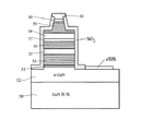
本発明にかかる実施例16の窒化物半導体素子は、図3に示すレーザダイオードである。
Example 16
The nitride semiconductor device of Example 16 according to the present invention is the laser diode shown in FIG.
実施例16のレーザダイオードは、80μmの厚さのGaN基板50上に、
(1)3μmの厚さのSiドープのGaNよりなるn型GaN層52、
(2)0.1μmの厚さのIn0.1Ga0.9N層53、
(3)第1の窒化物半導体層と第2の窒化物半導体層とからなる超格子構造のn側多層膜層54、
(4)Siがドープされた0.1μmの厚さのn型GaN光ガイド層55、
(5)In0.4Ga0.6N/In0.02Ga0.98N多重量子井戸構造の活性層56、(6)Mgがドープされた200オングストロームの厚さのAl0.2Ga0.8N層57、
(7)Mgがドープされた0.1μmの厚さのp型GaN光ガイド層58、
(8)第3の窒化物半導体層と第4の窒化物半導体層からなる超格子構造のp側多層膜層59、
(9)Mgがドープされた0.05μmの厚さのp型GaNコンタクト層60、以上の各層を成長させることにより作製される。
The laser diode of Example 16 is formed on a
(1) an n-
(2) In 0.1 Ga 0.9 N layer 53 having a thickness of 0.1 μm,
(3) an n-side
(4) an n-type GaN
(5) In 0.4 Ga 0.6 N / In 0.02 Ga 0.98 N multiple quantum well structure
(7) 0.1 μm-thick p-type GaN
(8) p-
(9) The p-type
なお、n側多層膜層54は、25オングストロームの厚さを有するアンドープのInGaNと、25オングストロームの厚さを有するSiドープのGaN層とが各240層、交互に積層されてなる。但し、アンドープのInGaNは、最初はIn0.01Ga0.99Nで成長させ、2回目以降はInの組成比を徐々に増加させ、最終の層がIn0.3Ga0.7Nとなるように組成傾斜している。
The n-side
また、活性層56は、それぞれ20オングストロームの厚さを有しSiがドープされた4つのIn0.4Ga0.6N井戸層が、50オングストロームの厚さを有しSiがドープされたIn0.02Ga0.98N障壁層と交互に設けられてなる。
The
また、p側多層膜層59は、25オングストロームの厚さを有しアンドープのAlGaN層と、25オングストロームの厚さを有しMgがドープされたGaN層とが各120層、交互に積層されてなる。但し、アンドープのAlGaNは、最初はAl0.01Ga0.99Nで成長させ、2回目以降はAlの組成比を徐々に増加させ、最終の層がAl0.2Ga0.8Nとなるように組成傾斜している。
Further, the p-side
本実施例16では、上記の(1)〜(9)の各層を形成した後、エッチングをすることにより、幅3μm、長さ450μmのリッジ形状とし、p型コンタクト層60上にAu/Niからなるp電極61を形成し、図3のように露出されたn型GaN層52上にTi/Alからなるn電極を形成する。
In Example 16, the layers (1) to (9) described above are formed and then etched to form a ridge shape having a width of 3 μm and a length of 450 μm. From the Au / Ni on the p-type contact layer 60 A p-
なお、リッジの両端面は、TiO2/SiO2を2ペア形成することにより、両端面の反射係数を50%にした。 In addition, the reflection coefficient of the both end surfaces was set to 50% by forming two pairs of TiO 2 / SiO 2 on both end surfaces of the ridge.
以上のようにして得られた実施例16のレーザダイオードは、良好な連続発振をする。 The laser diode of Example 16 obtained as described above oscillates satisfactorily.
1・・・サファイア基板
2・・・第1のバッファ層
3・・・第2のバッファ層
4・・・n側コンタクト層
5・・・第3のバッファ層
6・・・n側多層膜層
7・・・活性層
8・・・p側多層膜層
8’・・p側クラッド層
9・・・p側コンタクト層
10・・・全面電極
11・・・p電極
12・・・n電極
DESCRIPTION OF
Claims (11)
前記p側の窒化物半導体層には、Alを含む第3の窒化物半導体層と、第3の窒化物半導体と異なる組成を有する第4の窒化物半導体層とが積層されてなるp側多層膜層を有し、前記第3の窒化物半導体層、または前記第4の窒化物半導体の層の内の少なくとも一方の膜厚が100オングストローム以下であることを特徴とする窒化物半導体素子。 In a nitride semiconductor device having an active layer between an n-side nitride semiconductor layer and a p-side nitride semiconductor layer, the n-side nitride semiconductor layer includes In in contact with the active layer An n-side multilayer film in which a first nitride semiconductor layer and a second nitride semiconductor layer having a composition different from that of the first nitride semiconductor layer are stacked, and the first nitride semiconductor layer layer or at least one of the film thickness der 100 angstroms or less of said second nitride semiconductor layer, is,
The p-side nitride semiconductor layer includes a p-side multilayer formed by laminating a third nitride semiconductor layer containing Al and a fourth nitride semiconductor layer having a composition different from that of the third nitride semiconductor. It has a film layer, the third nitride semiconductor layer or the fourth nitride semiconductor device at least one of the thickness of the layers of nitride semiconductor, characterized in der Rukoto 100 angstroms or less.
Priority Applications (1)
| Application Number | Priority Date | Filing Date | Title |
|---|---|---|---|
| JP2004242880A JP4356555B2 (en) | 1998-03-12 | 2004-08-23 | Nitride semiconductor device |
Applications Claiming Priority (2)
| Application Number | Priority Date | Filing Date | Title |
|---|---|---|---|
| JP6023398 | 1998-03-12 | ||
| JP2004242880A JP4356555B2 (en) | 1998-03-12 | 2004-08-23 | Nitride semiconductor device |
Related Parent Applications (1)
| Application Number | Title | Priority Date | Filing Date |
|---|---|---|---|
| JP6258999A Division JP3622562B2 (en) | 1998-03-12 | 1999-03-10 | Nitride semiconductor light emitting diode |
Publications (3)
| Publication Number | Publication Date |
|---|---|
| JP2004343147A JP2004343147A (en) | 2004-12-02 |
| JP2004343147A5 JP2004343147A5 (en) | 2006-04-20 |
| JP4356555B2 true JP4356555B2 (en) | 2009-11-04 |
Family
ID=33542750
Family Applications (1)
| Application Number | Title | Priority Date | Filing Date |
|---|---|---|---|
| JP2004242880A Expired - Lifetime JP4356555B2 (en) | 1998-03-12 | 2004-08-23 | Nitride semiconductor device |
Country Status (1)
| Country | Link |
|---|---|
| JP (1) | JP4356555B2 (en) |
Families Citing this family (14)
| Publication number | Priority date | Publication date | Assignee | Title |
|---|---|---|---|---|
| JP3839799B2 (en) * | 2003-08-06 | 2006-11-01 | ローム株式会社 | Semiconductor light emitting device |
| JP2007214384A (en) | 2006-02-09 | 2007-08-23 | Rohm Co Ltd | Nitride semiconductor element |
| JP5068020B2 (en) * | 2006-02-20 | 2012-11-07 | シャープ株式会社 | Manufacturing method of nitride semiconductor light emitting device |
| KR101239851B1 (en) * | 2006-03-24 | 2013-03-06 | 서울옵토디바이스주식회사 | GaN-BASED COMPOUND SEMICONDUCTOR AND THE FABRICATION METHOD THEREOF |
| KR100835116B1 (en) * | 2007-04-16 | 2008-06-05 | 삼성전기주식회사 | Nitride semiconductor light emitting device |
| RU2369942C1 (en) | 2008-02-21 | 2009-10-10 | Самсунг Электро-Меканикс Ко., Лтд. | Light-emitting instrument based on nitride semiconductor |
| JP4640427B2 (en) | 2008-03-14 | 2011-03-02 | ソニー株式会社 | GaN-based semiconductor light-emitting device, light-emitting device assembly, light-emitting device, method for manufacturing GaN-based semiconductor light-emitting device, driving method for GaN-based semiconductor light-emitting device, and image display device |
| JP4655103B2 (en) | 2008-04-14 | 2011-03-23 | ソニー株式会社 | GaN-based semiconductor light-emitting device, light-emitting device assembly, light-emitting device, driving method for GaN-based semiconductor light-emitting device, and image display device |
| JP4940317B2 (en) | 2010-02-25 | 2012-05-30 | 株式会社東芝 | Semiconductor light emitting device and manufacturing method thereof |
| KR101140679B1 (en) | 2010-06-08 | 2012-04-25 | 서울옵토디바이스주식회사 | GaN-BASED COMPOUND SEMICONDUCTOR |
| JP5613719B2 (en) * | 2010-08-26 | 2014-10-29 | 株式会社東芝 | Semiconductor light emitting device |
| KR20130079873A (en) * | 2012-01-03 | 2013-07-11 | 엘지이노텍 주식회사 | Light emitting device and lighting system including the same |
| JP2014049595A (en) * | 2012-08-31 | 2014-03-17 | Ushio Inc | Nitride semiconductor element |
| JPWO2014178248A1 (en) | 2013-04-30 | 2017-02-23 | シャープ株式会社 | Nitride semiconductor light emitting device |
-
2004
- 2004-08-23 JP JP2004242880A patent/JP4356555B2/en not_active Expired - Lifetime
Also Published As
| Publication number | Publication date |
|---|---|
| JP2004343147A (en) | 2004-12-02 |
Similar Documents
| Publication | Publication Date | Title |
|---|---|---|
| JP3622562B2 (en) | Nitride semiconductor light emitting diode | |
| KR100574738B1 (en) | Nitride Semiconductor Device | |
| JP3868136B2 (en) | Gallium nitride compound semiconductor light emitting device | |
| JP3744211B2 (en) | Nitride semiconductor device | |
| JP4629178B2 (en) | Nitride semiconductor device | |
| JP3460641B2 (en) | Nitride semiconductor device | |
| JP3680558B2 (en) | Nitride semiconductor device | |
| JP2001237457A (en) | Light-emitting element | |
| JPH08228025A (en) | Nitride semiconductor light emitting element | |
| JP2001168471A (en) | Nitride semiconductor light-emitting element | |
| JP4356555B2 (en) | Nitride semiconductor device | |
| JP2002033512A (en) | Nitride semiconductor light emitting diode | |
| JP2002305323A (en) | n-TYPE NITRIDE SEMICONDUCTOR LAMINATE AND SEMICONDUCTOR DEVICE USING IT | |
| JP2000133883A (en) | Nitride semiconductor element | |
| JP4815732B2 (en) | Nitride semiconductor device | |
| JP3620292B2 (en) | Nitride semiconductor device | |
| JP3275810B2 (en) | Nitride semiconductor light emitting device | |
| JP3951973B2 (en) | Nitride semiconductor device | |
| JP4622466B2 (en) | Nitride semiconductor device | |
| JP3448196B2 (en) | Nitride semiconductor light emitting device | |
| JP4085782B2 (en) | Nitride semiconductor device | |
| JP3924973B2 (en) | Nitride semiconductor light emitting device manufacturing method and nitride semiconductor light emitting device | |
| JP3857417B2 (en) | Nitride semiconductor device | |
| JP4931271B2 (en) | Nitride semiconductor element and light emitting device using the same | |
| JP3952079B2 (en) | Manufacturing method of nitride semiconductor light emitting device |
Legal Events
| Date | Code | Title | Description |
|---|---|---|---|
| A521 | Written amendment |
Free format text: JAPANESE INTERMEDIATE CODE: A523 Effective date: 20060306 |
|
| A621 | Written request for application examination |
Free format text: JAPANESE INTERMEDIATE CODE: A621 Effective date: 20060306 |
|
| TRDD | Decision of grant or rejection written | ||
| A01 | Written decision to grant a patent or to grant a registration (utility model) |
Free format text: JAPANESE INTERMEDIATE CODE: A01 Effective date: 20090714 |
|
| A01 | Written decision to grant a patent or to grant a registration (utility model) |
Free format text: JAPANESE INTERMEDIATE CODE: A01 |
|
| A61 | First payment of annual fees (during grant procedure) |
Free format text: JAPANESE INTERMEDIATE CODE: A61 Effective date: 20090727 |
|
| FPAY | Renewal fee payment (event date is renewal date of database) |
Free format text: PAYMENT UNTIL: 20120814 Year of fee payment: 3 |
|
| R150 | Certificate of patent or registration of utility model |
Free format text: JAPANESE INTERMEDIATE CODE: R150 |
|
| FPAY | Renewal fee payment (event date is renewal date of database) |
Free format text: PAYMENT UNTIL: 20120814 Year of fee payment: 3 |
|
| FPAY | Renewal fee payment (event date is renewal date of database) |
Free format text: PAYMENT UNTIL: 20120814 Year of fee payment: 3 |
|
| FPAY | Renewal fee payment (event date is renewal date of database) |
Free format text: PAYMENT UNTIL: 20120814 Year of fee payment: 3 |
|
| FPAY | Renewal fee payment (event date is renewal date of database) |
Free format text: PAYMENT UNTIL: 20130814 Year of fee payment: 4 |
|
| R250 | Receipt of annual fees |
Free format text: JAPANESE INTERMEDIATE CODE: R250 |
|
| R250 | Receipt of annual fees |
Free format text: JAPANESE INTERMEDIATE CODE: R250 |
|
| R250 | Receipt of annual fees |
Free format text: JAPANESE INTERMEDIATE CODE: R250 |
|
| R250 | Receipt of annual fees |
Free format text: JAPANESE INTERMEDIATE CODE: R250 |
|
| R250 | Receipt of annual fees |
Free format text: JAPANESE INTERMEDIATE CODE: R250 |
|
| R250 | Receipt of annual fees |
Free format text: JAPANESE INTERMEDIATE CODE: R250 |
|
| EXPY | Cancellation because of completion of term |