JP4355443B2 - Double digital low IF composite receiver - Google Patents
Double digital low IF composite receiver Download PDFInfo
- Publication number
- JP4355443B2 JP4355443B2 JP2000389165A JP2000389165A JP4355443B2 JP 4355443 B2 JP4355443 B2 JP 4355443B2 JP 2000389165 A JP2000389165 A JP 2000389165A JP 2000389165 A JP2000389165 A JP 2000389165A JP 4355443 B2 JP4355443 B2 JP 4355443B2
- Authority
- JP
- Japan
- Prior art keywords
- components
- signal
- bandwidth
- communication receiver
- digital
- Prior art date
- Legal status (The legal status is an assumption and is not a legal conclusion. Google has not performed a legal analysis and makes no representation as to the accuracy of the status listed.)
- Expired - Fee Related
Links
Images


Classifications
-
- H—ELECTRICITY
- H04—ELECTRIC COMMUNICATION TECHNIQUE
- H04B—TRANSMISSION
- H04B1/00—Details of transmission systems, not covered by a single one of groups H04B3/00 - H04B13/00; Details of transmission systems not characterised by the medium used for transmission
- H04B1/69—Spread spectrum techniques
- H04B1/707—Spread spectrum techniques using direct sequence modulation
-
- H—ELECTRICITY
- H04—ELECTRIC COMMUNICATION TECHNIQUE
- H04B—TRANSMISSION
- H04B1/00—Details of transmission systems, not covered by a single one of groups H04B3/00 - H04B13/00; Details of transmission systems not characterised by the medium used for transmission
- H04B1/06—Receivers
- H04B1/16—Circuits
- H04B1/30—Circuits for homodyne or synchrodyne receivers
-
- H—ELECTRICITY
- H03—ELECTRONIC CIRCUITRY
- H03D—DEMODULATION OR TRANSFERENCE OF MODULATION FROM ONE CARRIER TO ANOTHER
- H03D7/00—Transference of modulation from one carrier to another, e.g. frequency-changing
- H03D7/16—Multiple-frequency-changing
- H03D7/165—Multiple-frequency-changing at least two frequency changers being located in different paths, e.g. in two paths with carriers in quadrature
- H03D7/166—Multiple-frequency-changing at least two frequency changers being located in different paths, e.g. in two paths with carriers in quadrature using two or more quadrature frequency translation stages
-
- H—ELECTRICITY
- H04—ELECTRIC COMMUNICATION TECHNIQUE
- H04B—TRANSMISSION
- H04B1/00—Details of transmission systems, not covered by a single one of groups H04B3/00 - H04B13/00; Details of transmission systems not characterised by the medium used for transmission
- H04B1/38—Transceivers, i.e. devices in which transmitter and receiver form a structural unit and in which at least one part is used for functions of transmitting and receiving
- H04B1/40—Circuits
- H04B1/403—Circuits using the same oscillator for generating both the transmitter frequency and the receiver local oscillator frequency
- H04B1/406—Circuits using the same oscillator for generating both the transmitter frequency and the receiver local oscillator frequency with more than one transmission mode, e.g. analog and digital modes
Landscapes
- Engineering & Computer Science (AREA)
- Computer Networks & Wireless Communication (AREA)
- Signal Processing (AREA)
- Power Engineering (AREA)
- Digital Transmission Methods That Use Modulated Carrier Waves (AREA)
- Compression, Expansion, Code Conversion, And Decoders (AREA)
Description
【0001】
【発明の属する技術分野】
この発明は通信受信機に関し、かつより特定的には広帯域符号分割多元接続(Wide Band Code Division Multiple Access:WBCDMA)のようなあるモードにおける広帯域信号を、かつまた、欧州セルラ電話システムGSM(グローバル・システム・モービル:Global System Mobile)が1つの例である、時分割多元接続(TDMA)のような他のモードに対する中帯域または狭帯域信号を受信することができる受信機に関する。
【0002】
【従来の技術】
今日の通信システム、例えばセルラ電話通信システム、は狭帯域または中帯域技術で動作する。前記GSMセルラ電話システム、時分割多元接続(TDMA)システム、はそのような中帯域システムの1つである。例えば、データまたはビデオ伝送に対するより高速の送信の要求が増大するに応じて、より広い帯域の技術がより望ましいものになってくる。セルラ通信のための1つのそのような広帯域技術は広帯域符号分割多元接続(WBCDMA)である。新しい技術が発展するに応じて、1つより多くの通信システムで動作して1つのシステムから他のものへと推移できるようにしあるいはユーザが両方のシステムの組み合わされた能力および特徴(フィーチャ:features)へとアクセスできるようにする通信機器を提供することが一般的になっている。したがって、通信受信機が狭帯域または中帯域のシステムからかつまた広帯域通信システムの双方から信号を受信できることが必要とされる。
【0003】
単一の広帯域および中帯域受信機を提供するための今日の努力は各々のモードに対して異なる受信機データ経路を提供することによって各々のモードに対する受信機回路を単に2重化した受信機設計を生じる結果となっている。一例として、ヨーロッパにおいて現在開発されている前記広帯域CDMAシステム、万能移動電話システム(Universal Mobile Telephone System:UMTS)、においては、チャネル帯域幅は3.84MHzであり、一方現在の欧州セルラシステム、GSM、は200KHzの帯域幅を有している。これらのシステムの双方はIQ変調モードで動作し、その場合送信されるべき情報は、適切に符号化された後、キャリヤ信号に重畳された同相および直角位相変調成分において提供され複素信号または複合信号を生成し、これはその後受信機によってデコードされて元の符号化された情報を出現させることになる。
【0004】
【発明が解決しようとする課題】
現在これら2つのモードは異なるダウンコンバージョン・ミキサ、ブロッキング・フィルタ、増幅器、アンチエイリアシング・フィルタ(antialiasing filters)、およびアナログ−デジタル変換器を備えた2つの異なる受信機回路を設けることによって1つの通信受信機ユニット内へと組み合わされている。前記受信機回路の各々は従って送信された信号のIおよびQ成分を受信しかつデコードすることができる別個の受信機である。
【0005】
したがって、いくつかのモードで動作可能でありかつ回路の多くの要素が各モードで使用可能であり、従って受信機において必要な回路の数を低減することにより受信機の複雑さを低減する単一の通信受信機を提供することが有利であろう。
【0006】
前記WBCDMA UMTSシステムの帯域幅は3.84MHzであるから、前記WBCDMA信号の各々のIおよびQ成分は3.84MHz/2の範囲にあることになる。これらの広い帯域幅は、送信信号の要求されるダイナミックレンジが与えられれば、フラッシュ(Flash)またはパイプライン化(Pipelined)データコンバータのような複雑なデータコンバータまたはデータ変換器を使用することを必要とし、該データコンバータは、非常に高速であるためスペクトル拡散システムにおける送信された符号を再生するために符号のトラッキングを可能とするよう高いサンプリングレートを許容するが、GSMモードにとって特に適したものではなく、それはこれらのデータコンバータは高い電力消費および限られたダイナミックレンジ(10ビット)を有するのに対しGSMモードは高いダイナミックレンジ(14ビット)を必要とするが低いサンプリングレートを許容するためである。より低い電力消費は、もちろん、セルラ電話のような携帯用または移動通信機器においては常に望ましいものである。前記GSMモードは異なる帯域幅に対して容易にプログラム可能であり、より広いダイナミックレンジを有し、かつ電力消費が少ないシグマ−デルタ(Sigma−Delta)デジタル−アナログ変換器または他の変換器を使用できるようにする。
【0007】
【課題を解決するための手段】
上述のおよび他の利点はある広帯域チャネルのサブバンド(sub−bands)をデュアル低中間周波(IF)デジタル手法を使用してII,IQ,QI,QQと称されるより狭い帯域幅成分へと重ね合わせる(superimpose)ことによって得ることができ、この場合各々の成分は中帯域幅または狭帯域幅モードが選択された場合に再使用できる共通のデータコンバータを使用することができる。
【0008】
これは送信のために広帯域または狭帯域のキャリアへと符号化されかつ変調された情報を伝達する無線信号を検出しかつ復調するためのデュアルモード通信受信機を提供することによって達成でき、該通信受信機は検出された帯域をサブバンドへと再分割しかつ該サブバンドを該サブバンドの帯域幅と同様の帯域幅を備えた複数の成分へと重ね合わせるための手段、各々の成分に別個に含まれる情報の部分を処理するための手段、および前記成分からの処理された情報を組み合わせて送信された元の情報を再現するための手段を具備する。
【0009】
これはまた送信のために広いまたは狭い帯域幅のキャリアへと符号化されかつ変調された情報を伝達する無線信号を検出しかつ復調するためのデュアルモード通信受信機を動作させる方法を提供することによって達成でき、該方法は、検出された信号を検出されたサブバンドへと再分割する段階、前記検出されたサブバンドを前記サブバンドの帯域幅と同じまたは同様の帯域幅を備えた複数の成分へと重ね合わせる段階、各々の成分に別個に含まれる情報の部分を処理する段階、および前記成分からの処理された情報を組み合わせて元の送信された情報を再現する段階を具備する。
【0010】
【発明の実施の形態】
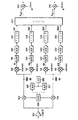
図1は、本発明に係わる通信受信機の全体のブロック図である。入力信号Vinは前に述べたように無線周波または中間周波チャネルへと変換されるベースバンド・スペクトルを表わす複素または複合信号であり、同相(In−phase)および直角位相(Quadrature−phase)成分を有する入力信号を生成するために送信機における変調器によって加えられる情報を有し、該入力信号Vinは増幅器100に印加され、該増幅器100の出力は2つの直交ミキサまたはダウンコンバータ102,104に供給される。入力信号VinはBWの帯域幅を有する。入力信号Vinは4つのサブバンドへと再分割される。
【0011】
IQダウンコンバータ102,104は無線周波信号(RF)または中間周波(IF)チャネルを、例えば、ギルバート型ミキサ(Gilbert Typeof Mixer)またはチョッパ型ミキサ(Chopper Type of Mixer)を使用してDCスペクトルへとダウンコンバートする。
【0012】
局部発振器(Local Oscillator)105は2つのアナログ−デジタル変換器106および107をドライブして直交アナログ出力(sin(wt)およびcos(wt)、この場合w=2*Pi*BW/4)を生成し、これらは次に直交ネットワーク108をドライブし、該直交ネットワーク108は2つのRFまたはIF発振器信号を伝達するためにPi/2で分割または除算し、これらの信号は直交ミキサ102,104の2つの局部発振器ポートに供給するために直交している。
【0013】
ミキサ102および104の出力はベースバンドまたは低中間周波数における(以後、ベースバンドへの言及は代わりに、受信機の設計に応じて、低中間周波を含むことがある)入力信号Vinの直交表現である。
【0014】
ミキサ102および104の出力は第1のローパス・ブロッキングフィルタ(容量)によってろ波されかつ次にそれぞれさらに他のミキサ(乗算器)110,112,114および116に供給され、これらのミキサにおいて帯域幅BW/2のIおよびQサブバンド成分はさらに帯域幅BW/4の4つの成分II,IQ,QIおよびQQへと分割される。これら4つの成分は増幅されかつ、各々BW/4に等しいかまたはそれより大きな帯域幅を有する、ローパスフィルタ118,120,122および124によってさらなるブロッキングろ波(blocking filtering)を行なうためにろ波される。
【0015】
前記ミキサはIおよびQ IFまたはRFからベースバンドへのミキサ102および104を除き低周波ミキサ/乗算器である。該ミキサ/乗算器110,112,114および116は利得を有する乗算器DACとして実施することができ、この場合デジタル入力ポートは供給されるcos(wt)およびsin(wt)のデジタル表現を有しかつ前記アナログ入力ポートはミキサ102および104のろ波された出力である。乗算器DACのクロック周波数はこのクロックの高調波におけるスプリアス応答を避けるために前に設けられるブロッキングの量に依存する。また、この乗算器DACは受信機における自動利得制御(AGC)信号を設定するために使用できる。
【0016】
前記ローパスフィルタは一般に広帯域または中帯域または狭帯域がろ波できるようにプログラム可能なカットオフ周波数を備えたアクティブまたは能動RC型のフィルタに基づいている。これらのフィルタはBW/4に等しい帯域幅を有し、これは同様のブロッキング排除要求を備えたBW/2に等しい帯域幅のフィルタに対してそれらの設計を簡略化する。これは前記フィルタがフィルタごとに要求されるポールの数を低減できるようにし、それは次により少ないグループまたは群および振幅リップルを導入することになる。また、プログラミングのカットオフ周波数範囲が低減される。
【0017】
ローパスフィルタ118,120,122および124の出力は、シグマ−デルタA/D変換器とすることができる、アナログ−デジタル変換器126,128,130および132、ならびにデシメイション・フィルタ134,136,138および140へと供給され後に詳細に説明する成分信号IIf,IQf,QIfおよびQQfを生成する。該信号はコンバイナ142において利得および位相修正されかつ再結合されて出力信号Vout++およびVout−+を生成する。これらの出力信号はその後復調されかつデコードされて送信機の変調器によって前記複素または複合入力信号へと前に符号化された情報を表わすデジタルビットストリームを生成する。
【0018】
アナログ−デジタル変換器126,128,130および132は好ましくは種々の広帯域または中帯域または狭帯域信号成分に対してオーバサンプリング比をプログラム可能なシグマ−デルタ型のA/D変調器である。前記成分II,IQ,QI,QQはそれらの帯域幅が各々BW/4に低減されているから、これは同じダイナミックレンジに対してシグマ−デルタに対するオーバサンプリングの要求されるオーバサンプリング・クロック周波数を低減する。例えば、BW=3.84MHzを有するWBCDMAモードにおいては、前記オーバサンプリングクロックは26MHzの範囲において選択されそれによって10ビットの分解能に対して26MHz/(3.84MHz/4)=27.08の範囲になるようにされ、一方、GMSモードにおいては、前記オーバサンプリングクロックは14ビットの分解能に対してオーバサンプリング比13MHz/0.2KHz=65に対し13MHzとなる。
【0019】
前記シグマ−デルタ変調器126,128,130および132はオーバサンブリングの特定周波数でオーバサンプルされたデジタルストリームを発生する。これらのデジタル出力はこの種の変調器にとって典型的であるようにシグマ−デルタ変調器の次数(order)および形式に応じて成形されたノイズスペクトルを含む。前記デジタル出力は次にデジタル的にろ波されてシグマ−デルタ変調器の前記成形されたノイズを除去し、かつ次に選択ろ波(selectivity filtering)を行なうためにより低いクロックレートで動作するデシメイション・デジタルフィルタ134,136,138および140によってさらに処理するためにより低いクロック周波数へとデシメイトされる。デジタル出力IIf,IQf,QIfおよびQQfは次にコンバイナ142におけるデジタル乗算器および加算器によって処理されて利得および位相の不平衡の修正を行ないかつベクトルVout++およびVout−+で表わされる4つのデジタル出力成分を発生する。
【0020】
アナログフィルタ118,120,122および124、シグマ−デルタ変換器126,128,130および132、およびデジタル・デシメイションフィルタ134,136,138および140の帯域幅はまたいくつかの帯域幅設定を取り扱うためにプログラム可能にすることができる。
【0021】
図1に示される好ましい実施形態においては、受信機が示されており、該受信機においては、入力信号は4つの成分に分割される。しかしながら、入力信号の帯域幅および前記成分の所望の帯域幅に応じて異なる数の成分を使用できることが理解されるであろう。
【0022】
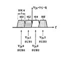
図1の受信機の動作は図2〜図5に示される受信機における種々のポイントでの信号のスペクトル表現を参照することにより最もよく理解することができる。増幅器100に印加される入力チャネルは図2においてそれぞれ、以後sub0,sub1,sub2およびsub3と称されかつ参照数字160,162,164および166によって参照される4つのサブバンドへと再分割または細分される。図2は4つのサブバンドへと分割された後のVinのスペクトル表現である。前記サブバンドの各々はBW/4の帯域幅を有する。
【0023】
これら4つのサブバンドの基礎を成すRFチャネルはRFまたはIF周波数から、ミキサ102および104の出力として、2つの成分、IおよびQ、においてベースバンドへとダウンコンバートされ、これらの出力は直交位相関係にありかつ各々の成分はBW/2(0からBW/2)のスペクトル帯域幅を有する。
【0024】
もしベクトルVin=I+j・Qがベースバンドにおける入力チャネルの表現であるとすれば、Vinは前記4つのサブバンドに対応する4つのベクトルの合計として表現することができ、例えば、Vin=Vin0+Vin1+Vin2+Vin3となる。図2はまたこの表現を示し、そこではVin0はsub0に対応し、Vin1はsub1に対応し、Vin2はsub2に対応し、そしてVin3はsub3に対応する。
【0025】
図3(a)および図3(b)は、その構成要素IおよびQ成分(ラインf上)で表現されたVinのスペクトルを示す。したがって、Vinの実数部、例えば、I=I0+I1+I2+I3はそれぞれ図3(b)において160I,162I,164Iおよび166Iとして示され、かつ虚数部はj・Q=j・Q0+j・Q1+j・Q2+j・Q3はそれぞれ図3(a)において160Q,162Q,164Qおよび166Qとして示されている。
【0026】
それから、前に述べたように、sub3,166はsub0,160と混合され、sub2,164はsub1,162と混合され、再び前記fラインの下にIおよびj・Qスペクトルが別個に見られる。
【0027】
各々の成分IおよびQは次にミキサ110,112,114および116において低IF直交信号cos(wt)およびsin(wt)と混合され(この場合、w=2・pi・BW/4または最も近い値である)、すなわち前記低IFクロックはIまたはQ帯域幅の半分である。該動作は次のようになる。
【数1】
IIf=II**HII, II=Icos(wt)
IQf=IQ**HIQ, IQ=Isin(wt)
QIf=QI**HQI, QI=Qcos(wt)
QQf=QQ**HQQ, QQ=Qsin(wt)
【0028】
この場合、HII,HIQ,HQIおよびHQQは、それぞれ、前記II,IQ,QIおよびQQ経路における、それぞれ、アナログおよびデジタルフィルタ118,120,122および124、および134,136,138および140の伝達関数である。
前記**は時間領域のたたみ込み(convolution)を意味する。
【0029】
【数2】
II=I・(e+j(wt)+e−j(wt))/2
IQ=I・(e+j(wt)−e−j(wt))/2j
QI=Q・(e+j(wt)+e−j(wt))/2
QQ=Q・(e+j(wt)−e−j(wt))/2j
【0030】
e+j(wt)による乗算はスペクトルを+wだけ、すなわち、+BW/4だけシフトすることと等価である。e−j(wt)による乗算は−wだけ、すなわち−BW/4だけスペクトルをシフトすることと等価である。
【0031】
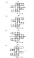
結果として図4(a)、図4(b)、図4(c)および図4(d)に示されるスペクトルになり、これらの図はまたそれぞれ前記フィルタ118,120,122および124の出力を、各々図面に示される、II,IQ,QIおよびQQとして図式的に示す。帯域幅BW/2のフィルタとしてかつ、それぞれ、IIf,IQf,QIfおよびQQfとしてフィルタ134,136,138および140の出力も帯域幅W/2のフィルタとして示されている。上で述べたスペクトルのシフトもまた図4に図式的に示されている。前記II,IQ,QIおよびQQ経路におけるフィルタの出力の各々は前記4つのサブバンドの各々を含み、これが成分II,IQ,QIおよびQQが図4(a)〜図4(d)に示されるように、重ね合わされた4つのサブバンドを有する理由であり、かつ従って入力信号Vin内に元々含まれる全ての情報が元の信号を再現するために利用または入手可能であるが、信号の処理は元の信号Vinよりも狭い帯域幅において行なわれ従って広い帯域幅をサポートするためこの動作を行なうために通常使用されるフラッシュまたはパイプライン化データコンバータではなくシグマ−デルタA/D変換器によって達成できる。
【0032】
送信された元の(しかしながら、今や処理された)情報の再現の形式で出力を生成するため、前記4つのサブバンドの各々の情報はコンバイナ142において再結合されて2つのベクトル成分Vout++およびVout−+を形成しなければならない。
【数3】
Vout++=(IIf−QQf)
+j・(IQf+QIf)
Vout−+=(IIf+QQf)
+j・(−IQf+QIf)
【0033】
したがって、それぞれ図5(a)および図5(b)に図式的に示されるように、前記Vout++ベクトルはサブバンド0およびサブバンド1、160および162、の再現に対応し、かつ前記Vout−+ベクトルはサブバンド2およびサブバンド3、164および166、の再現に対応する。コンバイナ142による再結合はいくつかの方法で行なわれ、例えば次のように行なうことができる。
Vout++に対してIIf−QQf=I++を達成するため加算器/減算器を使用する。
Vout++に対してIQf+QIf=Q++を達成するため加算器/減算器を使用する。
Vout−+に対してIIf+QQf=I−+を達成するため加算器/減算器を使用する。
Vout−+に対して−IQf+QIf=Q−+を達成するため加算器/減算器を使用する。
【0034】
前記演算操作Vout++e−j(wt)は複素乗算器を使用して形成され、加算器および乗算器を使用して次のデジタル演算操作を行なう。すなわち、(I++ +j・Q++)・(cos(wt)−j・sin(wt))=I++・cos(wt)+Q++・sin(wt)+j・(−I++・sin(wt)+Q++・cos(wt))
【0035】
演算操作Vout−+ej(wt)は複素乗算器を使用して形成され、加算器および乗算器を使用して次のデジタル演算操作を行なう。すなわち、(I−+ +j・Q−+)・(cos(wt)+j・sin(wt))=I−+・cos(wt)−Q−+・sin(wt)+j・(I−+sin(wt)+Q−+・cos(wt))
【0036】
前記成分IIf,IQf,QIfおよびQQfの4つ全ては各々のサブバンドを再現するために必要とされることに注意を要する。サブバンドを別個に復元するために4つ全ての成分が利用できることが要求される。各々の成分(II,IQ,QIおよびQQ)は前記BW/4の中にそれらのそれぞれのスペクトルで示されるように4つのサブバンド全てに関連する情報を含んでいる。これが受信機が4つのサブバンド全てを並列に処理することができるようにしかつより好ましいA/D変換技術を使用できるようにする。このため、前記受信機は2重デカルト(ダブル・カーテシアン:Double Cartesian)受信機と称することができ、それは各々のサブバンドを再現するために前記4つの成分が必要とされるからである。
【0037】
また、これら4つの実数成分はBW/4のスペクトル幅を有しかつこれら4つの成分をデジタル化するために同じローパスA/D変換器を備えた同じローパスフィルタが必要とされることに注意を要する。
【0038】
本発明を採用した受信機はBW/4の帯域幅要求を有するIIf,QQf,QIfおよびIQfと称される4つのベースバンド出力成分(2重デカルト)を備えた帯域幅BWのRFまたはIF入力チャネルを有する受信機とみることができる。元のスペクトルを再現し戻すため、2つの再現ベクトルVout++およびVout−+がそれぞれ−wだけかつ+wだけシフトされることが必要であり、かつそれぞれe−j(wt−phi0)およびe+j(wt−phi0)で乗算されることが必要である。
【0039】
【数4】
Vout r
=Vout++・e−j(wt−phi0)
+Vout−+・e+j(wt−phi0)
この場合、phi0は位相の不連続を除去するよう選択される。sin(wt)およびcos(wt)が発生される必要があるから、sin(wt)およびcos(wt)を発生した位相発生器は単に−phi0のオフセットでスタートする。
【0040】
Vout++およびVout−+をそれらの表現で置き換えることにより次の式を得る。
【数5】
Vout r=2(IIf・cos(wt−phi0)
+IQf・sin(wt−phi0))
+2・j・(QIf・cos(wt−phi0)
+QQf・sin(wt−phi0))
【0041】
すなわち、再現された同相および直角位相成分は次のようになる。
【数6】
Ir=(IIf・cos(wt−phi0)
+IQf・sin(wt−phi0))
Qr=(QIf・cos(wt−phi0)
+QQf・sin(wt−phi0))
【0042】
上で述べた数式に従って再現されたベクトルVout rの実数および虚数出力を発生するためかつまた前記4つの経路によって導入される不整合に対する利得および位相修正を提供するためにコンバイナ142の再現構成が図6に示されている。図6において実施される再結合方程式Ir=(IIf・cos(wt−phi0)+IQf・sin(wt−phi0))およびQr=(QIf・cos(wt−phi0)+QQf・sin(wt−phi0))はまたそれらがそれらの間で整合しない場合に前記成分の間の利得および位相修正を使用する。
【0043】
IIfは利得修正項Kiiによって乗算され、IQfは利得修正項Kiqによって乗算され、QQfは利得修正項Kqqによって乗算され、かつQIfは利得修正項Kqiによって乗算され、これらの乗算はそれぞれ乗算器170,172,174および176によって行なわれる。前記利得修正項は修正された各項が等しい振幅になるよう選択される。
【0044】
さらに、IIf,IQf,QIfおよびQQfの間で位相を修正することが必要とされる。例えば、IIfをcos(wt−phi0)により、乗算するよりはむしろ、それは乗算器178においてcos(wt−phi0+PhiIQ)によって乗算され、この場合PhiIQはIIfおよびIQfの間の位相の不整合を補償するためにIQfに対してIIfの位相をシフトするために使用される位相値である。同様に、前記項PhiQIは乗算器180において適用されるQIfおよびQQfの間の位相不整合を補償するための位相修正である。
【0045】
いったんIIfおよびIQfが利得および位相整合されると、かつQIfおよびQQfが利得および位相整合されると、(IIf,IQf)、加算器182の出力、および(QQf,QIf)、加算器184の出力、は位相が整合されなければならない。これは加算器182の出力に加算器184の出力である項Kriを加算することによって行なわれる。これは単に次の式で説明できる。
【数7】
cos(wt+PhiIR)
=cos(wt)cos(PhiIR)
+sin(wt)・sin(PhiIR)
【0046】
これは、位相値PhiRによって修正するために、虚数部sin(wt)(加算器184の出力)がとられかつKri=sin(PhiIR)によって乗算され、そして加算器182の出力cos(wt)・cos(PhiIR)に加えられることを意味する。cos(PhiIR)による乗算の演算は加算器182の前にKii′=Kii・cos(PhrIR)およびKiq′=Kiq・cos(PhiIR)の変更によって達成でき乗算器を節約する。
【0047】
したがって次のようになる。
【数8】
Ir=Kii・cos(PhIR)
・Iff・cos(wt−phi0+PhiIQ)
+Kiq・cos(PhiIR)
・IQf・sin(wt−phi0)
+Qr・Kri、および
Qr=Kqq・QQf
・sin(wt−phi0−PhiQI)
+Kqi・QIf・cos(wt−phi0)
【0048】
前記受信信号が狭帯域幅または中帯域幅(これらの双方は本説明の目的で狭帯域と称することができ、その理由はそれらが前に述べた広帯域に対して狭いからである)を有する場合、すなわちBWよりはむしろBW/2のような場合(例えば、GSMセルラ電話信号)、前記受信機の成分の枝路の内の2つはオフに切り替えることができ、一方他の2つの枝路はオンに留めることができ、デジタル局部発振器が0に設定されまたは利得制御(AGC)を設定するために使用される。(すなわち、cos(wt)=1またはcos(wt)=AGCおよびsin(wt)=0である。)これは次に単一デカルト受信機として機能する。
【0049】
図1の受信機は図7においてそのようなモードで示されている。図6に示されるように、図7の受信機への入力は図1のものと同様に操作され、すなわち、局部発振器105、および局部発振器直交発生器108は前に述べたのと同じ信号を生成し、これは入力チャネルをベースバンドへと低減しかつスペクトルをそのIおよびQ直交成分へと分割するよう作用するミキサ102および104と同様である。しかしながら、図6の受信機においては、IQおよびQQ経路はそこへの入力信号を0によって乗算することによりディスエーブルされる。これは2つの経路のみがアクティブに留まることができるようにし、前記複合の、しかしながら、狭い、またはより狭い、帯域の入力信号のIおよびQ成分の各々に対して1つの経路を許容する。
【0050】
前記アクティブな経路IIおよびQIはそれぞれアナログのローパスフィルタ118および122において入力チャネルをろ波し、A/D変換器126および130(これはシグマ−デルタ変換器とすることができる)においてアナログ−デジタル変換を行ない、かつフィルタ134および138においてデジタルろ波を提供し、出力信号IoutおよびQoutを生成し、これらは次に送信機によって符号化された元の符号化情報を引き出すために使用される。
【0051】
理解できるように、このようにして広帯域および狭帯域の信号の双方が同じ受信機構成要素によって処理できかつ構成要素およびデータ経路の重複が避けられる。
【0052】
前に述べたように、上記好ましい実施形態においては、受信機は入力信号が4つの場合(または、中帯域または狭帯域信号の場合2つの成分)へと分割されるものとして説明されているが、入力信号の帯域幅および構成成分の所望の帯域幅に応じて異なる数の構成成分を使用できることが理解されるであろう。
【図面の簡単な説明】
【図1】本発明に係わる通信受信機全体の構成を示すブロック図である。
【図2】入力信号Vinのスペクトル表現を示す説明図である。
【図3】入力信号Vinのスペクトル表現を虚数部(a)および実数部(b)に分離して示す説明図である。
【図4】信号Vinである成分II,IQ,QIおよびQQの、サブバンドの各々をsin(wt)またはcos(wt)と混合しかつ前記成分の各々をろ波した後の、スペクトル表現を示す説明図である。
【図5】サブバンド0およびサブバンド1の再現に対応するVout++ベクトル、およびサブバンド2およびサブバンド3の再現に対応するVout−+ベクトルを図式的に示す説明図である。
【図6】本発明に係わるコンバイナ回路の構成を示す概略的ブロック回路図である。
【図7】狭帯域幅または中帯域幅信号の受信のための受信機の構成を示す本発明に係わる通信受信機の全体的なブロック図である。
【符号の説明】
100 増幅器
102,104 直交ミキサまたはダウンコンバータ
105局部発振器
106,107 A/D変換器
108 直交ネットワーク
110,112,114,116 ミキサ
118,120,122,124 ローパスフィルタ
126,128,130,132 A/D変換器
134,136,138,140 デシメイション・フィルタ
142 コンバイナ[0001]
BACKGROUND OF THE INVENTION
The present invention relates to communication receivers, and more particularly to broadband signals in certain modes such as Wide Band Code Division Multiple Access (WBCDMA), and also to the European cellular telephone system GSM (Global System Mobile: relates to a receiver capable of receiving medium or narrowband signals for other modes such as time division multiple access (TDMA), one example of which is Global System Mobile.
[0002]
[Prior art]
Today's communication systems, such as cellular telephone communication systems, operate with narrowband or mediumband technology. The GSM cellular telephone system, a time division multiple access (TDMA) system, is one such midband system. For example, as the demand for faster transmissions for data or video transmission increases, wider bandwidth technologies become more desirable. One such broadband technology for cellular communications is Wideband Code Division Multiple Access (WBCDMA). As new technologies evolve, they can operate in more than one communication system to allow transition from one system to another, or the combined capabilities and features of both systems (features: features). It has become common to provide communication devices that allow access to Therefore, it is required that the communication receiver be able to receive signals from both narrowband or mediumband systems and also from wideband communication systems.
[0003]
Today's efforts to provide a single wideband and midband receiver are receiver designs that simply duplicate the receiver circuit for each mode by providing a different receiver data path for each mode. As a result. As an example, in the broadband CDMA system currently developed in Europe, Universal Mobile Telephone System (UMTS), the channel bandwidth is 3.84 MHz, while the current European cellular system, GSM, Has a bandwidth of 200 KHz. Both of these systems operate in the IQ modulation mode, in which case the information to be transmitted is provided in the in-phase and quadrature modulation components superimposed on the carrier signal after being properly encoded and complex or composite signal Which is then decoded by the receiver to reveal the original encoded information.
[0004]
[Problems to be solved by the invention]
Currently these two modes receive one communication by providing two different receiver circuits with different down-conversion mixers, blocking filters, amplifiers, antialiasing filters, and analog-to-digital converters. Combined into the machine unit. Each of the receiver circuits is thus a separate receiver that can receive and decode the I and Q components of the transmitted signal.
[0005]
Thus, a single that can operate in several modes and many elements of the circuit can be used in each mode, thus reducing the complexity of the receiver by reducing the number of circuits required in the receiver. It would be advantageous to provide a communication receiver.
[0006]
Since the bandwidth of the WBCDMA UMTS system is 3.84 MHz, each I and Q component of the WBCDMA signal is in the range of 3.84 MHz / 2. These wide bandwidths necessitate the use of complex data converters or data converters such as flash or pipelined data converters given the required dynamic range of the transmitted signal. The data converter is so fast that it allows a high sampling rate to allow code tracking to recover the transmitted code in a spread spectrum system, but is not particularly suitable for GSM mode Not because these data converters have high power consumption and limited dynamic range (10 bits), while GSM mode requires high dynamic range (14 bits) but allows low sampling rates . Lower power consumption is, of course, always desirable in portable or mobile communication devices such as cellular phones. The GSM mode is easily programmable for different bandwidths, uses a sigma-delta digital-to-analog converter or other converter with a wider dynamic range and lower power consumption It can be so.
[0007]
[Means for Solving the Problems]
The above and other advantages are that subbands of certain wideband channels can be made into narrower bandwidth components called II, IQ, QI, QQ using dual low intermediate frequency (IF) digital techniques. Each component can use a common data converter that can be reused when medium bandwidth or narrow bandwidth mode is selected.
[0008]
This can be achieved by providing a dual mode communication receiver for detecting and demodulating a radio signal carrying information encoded and modulated onto a wideband or narrowband carrier for transmission, the communication Means for subdividing the detected band into subbands and superimposing the subbands into a plurality of components having a bandwidth similar to the bandwidth of the subbands, each component separately Means for processing the part of the information contained in and means for reproducing the original information transmitted by combining the processed information from said components.
[0009]
It also provides a method of operating a dual mode communication receiver for detecting and demodulating a radio signal carrying information encoded and modulated onto a wide or narrow bandwidth carrier for transmission And re-dividing the detected signal into detected subbands, wherein the detected subbands have a plurality of bandwidths having a bandwidth that is the same as or similar to the bandwidth of the subbands. Overlaying the components, processing portions of the information contained separately in each component, and combining the processed information from the components to reproduce the original transmitted information.
[0010]
DETAILED DESCRIPTION OF THE INVENTION
FIG. 1 is an overall block diagram of a communication receiver according to the present invention. The input signal Vin is a complex or composite signal representing a baseband spectrum that is converted to a radio frequency or intermediate frequency channel, as described above, and includes in-phase and quadrature-phase components. Having information added by a modulator at the transmitter to produce an input signal having the input signal Vin applied to an
[0011]
The
[0012]
A
[0013]
The outputs of the
[0014]
The outputs of
[0015]
The mixer is a low frequency mixer / multiplier except for I and Q IF or RF to
[0016]
The low-pass filter is generally based on an active or active RC type filter with a cut-off frequency that can be programmed to filter a wide band, a medium band or a narrow band. These filters have a bandwidth equal to BW / 4, which simplifies their design for filters with a bandwidth equal to BW / 2 with similar blocking exclusion requirements. This allows the filter to reduce the number of poles required per filter, which in turn introduces fewer groups or groups and amplitude ripples. Also, the programming cut-off frequency range is reduced.
[0017]
The outputs of the low pass filters 118, 120, 122 and 124 are analog to
[0018]
Analog-to-
[0019]
The sigma-
[0020]
The bandwidth of
[0021]
In the preferred embodiment shown in FIG. 1, a receiver is shown in which the input signal is divided into four components. However, it will be appreciated that different numbers of components can be used depending on the bandwidth of the input signal and the desired bandwidth of the components.
[0022]
The operation of the receiver of FIG. 1 can best be understood by referring to the spectral representation of the signal at various points in the receiver shown in FIGS. The input channels applied to
[0023]
The RF channel underlying these four subbands is downconverted from the RF or IF frequency to the baseband in two components, I and Q, as the outputs of
[0024]
If the vector Vin = I + j · Q is a representation of the input channel in the baseband, Vin can be represented as the sum of four vectors corresponding to the four subbands, for example, Vin = Vin0 + Vin1 + Vin2 + Vin3. . FIG. 2 also shows this representation, where Vin0 corresponds to sub0, Vin1 corresponds to sub1, Vin2 corresponds to sub2, and Vin3 corresponds to sub3.
[0025]
FIG. 3A and FIG. 3B show the spectrum of Vin expressed by its component I and Q components (on line f). Therefore, the real part of Vin, for example, I = I0 + I1 + I2 + I3 is shown as 160I, 162I, 164I and 166I in FIG. 3B, respectively, and the imaginary part is j · Q = j · Q0 + j · Q1 + j · Q2 + j · Q3 In FIG. 3A, they are shown as 160Q, 162Q, 164Q and 166Q.
[0026]
Then, as previously mentioned, sub3,166 is mixed with sub0,160, sub2,164 is mixed with sub1,162, and again I and j · Q spectra are seen separately under the f line.
[0027]
Each component I and Q is then mixed with a low IF quadrature signal cos (wt) and sin (wt) in
[Expression 1]
IIf = II ** HII, II = Icos (wt)
IQf = IQ ** HIQ, IQ = Isin (wt)
QIf = QI ** HQI, QI = Qcos (wt)
QQf = QQ ** HQQ, QQ = Qsin (wt)
[0028]
In this case, HII, HIQ, HQI and HQQ are the transfer functions of analog and
The ** means time domain convolution.
[0029]
[Expression 2]
II = I · (e+ J (wt)+ E-J (wt)) / 2
IQ = I · (e+ J (wt)-E-J (wt)) / 2j
QI = Q · (e+ J (wt)+ E-J (wt)) / 2
QQ = Q · (e+ J (wt)-E-J (wt)) / 2j
[0030]
e+ J (wt)Multiplication by is equivalent to shifting the spectrum by + w, ie + BW / 4. e-J (wt)Multiplication by is equivalent to shifting the spectrum by -w, i.e. -BW / 4.
[0031]
The result is the spectrum shown in FIGS. 4 (a), 4 (b), 4 (c) and 4 (d), which also show the outputs of the
[0032]
In order to produce an output in the form of a reproduction of the transmitted original (but now processed) information, the information of each of the four subbands is recombined in a
[Equation 3]
Vout ++ = (IIf−QQf)
+ J · (IQf + QIf)
Vout − + = (IIf + QQf)
+ J · (−IQf + QIf)
[0033]
Thus, as schematically shown in FIGS. 5 (a) and 5 (b), respectively, the Vout ++ vector corresponds to the reproduction of
An adder / subtracter is used to achieve IIf−QQf = I ++ for Vout ++.
An adder / subtracter is used to achieve IQf + QIf = Q ++ for Vout ++.
An adder / subtracter is used to achieve IIf + QQf = I− + for Vout− +.
An adder / subtracter is used to achieve -IQf + QIf = Q- + for Vout- +.
[0034]
The arithmetic operation Vout ++ e-J (wt)Is formed using a complex multiplier and performs the following digital arithmetic operations using the adder and multiplier. That is, (I ++ + j · Q ++) · (cos (wt) −j · sin (wt)) = I ++ · cos (wt) + Q ++ · sin (wt) + j · (−I ++ · sin (wt) + Q ++ · cos (wt) ))
[0035]
Arithmetic operation Vout- + ej (wt)Is formed using a complex multiplier and performs the following digital arithmetic operations using the adder and multiplier. That is, (I − ++ j · Q − +) · (cos (wt) + j · sin (wt)) = I− ·· cos (wt) −Q− ·· sin (wt) + j · (I− + sin ( wt) + Q-+. cos (wt))
[0036]
Note that all four of the components IIf, IQf, QIf and QQf are required to reproduce each subband. All four components are required to be available to restore the subbands separately. Each component (II, IQ, QI and QQ) contains information related to all four subbands in the BW / 4 as shown in their respective spectra. This allows the receiver to process all four subbands in parallel and to use the more preferred A / D conversion technique. For this reason, the receiver can be referred to as a double Cartesian receiver because the four components are needed to reproduce each subband.
[0037]
Also note that these four real components have a BW / 4 spectral width and the same low pass filter with the same low pass A / D converter is required to digitize these four components. Cost.
[0038]
A receiver employing the present invention has a bandwidth BW RF or IF input with four baseband output components (double Cartesian) called IIf, QQf, QIf and IQf with bandwidth requirements of BW / 4 It can be seen as a receiver having a channel. In order to reproduce the original spectrum, the two reproduction vectors Vout ++ and Vout− + need to be shifted by −w and + w respectively and e-J (wt-phi0)And e+ J (wt-phi0)It is necessary to be multiplied by.
[0039]
[Expression 4]
Vout r
= Vout ++ · e-J (wt-phi0)
+ Vout- + · e+ J (wt-phi0)
In this case, phi0 is selected to remove phase discontinuities. Since sin (wt) and cos (wt) need to be generated, the phase generator that generated sin (wt) and cos (wt) simply starts with an offset of -phi0.
[0040]
Replacing Vout ++ and Vout- + with their representation yields
[Equation 5]
Vout r = 2 (IIf.cos (wt-phi0))
+ IQf · sin (wt-phi0))
+ 2 · j · (QIf · cos (wt-phi0)
+ QQf · sin (wt-phi0))
[0041]
That is, the reproduced in-phase and quadrature components are as follows:
[Formula 6]
Ir = (IIf.cos (wt-phi0))
+ IQf · sin (wt-phi0))
Qr = (QIf · cos (wt-phi0)
+ QQf · sin (wt-phi0))
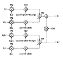
[0042]
The reproduction configuration of the
[0043]
IIf is multiplied by a gain correction term Kii, IQf is multiplied by a gain correction term Kiq, QQf is multiplied by a gain correction term Kqq, and QIf is multiplied by a gain correction term Kqi, which are multiplied by
[0044]
Furthermore, it is necessary to modify the phase between IIf, IQf, QIf and QQf. For example, rather than multiplying IIf by cos (wt-phi0), it is multiplied by cos (wt-phi0 + PhiIQ) in
[0045]
Once IIf and IQf are gain and phase matched and QIf and QQf are gain and phase matched, (IIf, IQf), the output of
[Expression 7]
cos (wt + PhiIR)
= Cos (wt) cos (PhiIR)
+ Sin (wt) · sin (PhiIR)
[0046]
This is corrected by the phase value PhiR, the imaginary part sin (wt) (output of adder 184) is taken and multiplied by Kri = sin (PhiIR), and the output cos (wt) · means added to cos (PhiIR). The operation of multiplication by cos (PhiIR) can be accomplished by changing Kii ′ = Kii · cos (PhrIR) and Kiq ′ = Kiq · cos (PhiIR) before the
[0047]
Therefore:
[Equation 8]
Ir = Kii · cos (PhIR)
・ Iff ・ cos (wt-phi0 + PhiIQ)
+ Kiq · cos (PhiIR)
IQf / sin (wt-phi0)
+ Qr · Kri, and
Qr = Kqq · QQf
・ Sin (wt-phi0-PhiQI)
+ Kqi, QIf, cos (wt-phi0)
[0048]
When the received signal has a narrow bandwidth or medium bandwidth (both of which can be referred to as narrow bandwidth for purposes of this description because they are narrow relative to the wide bandwidth previously described) That is, in cases such as BW / 2 rather than BW (eg GSM cellular telephone signal), two of the receiver component branches can be switched off, while the other two branches Can remain on and the digital local oscillator is set to zero or used to set gain control (AGC). (Ie cos (wt) = 1 or cos (wt) = AGC and sin (wt) = 0). This then functions as a single Cartesian receiver.
[0049]
The receiver of FIG. 1 is shown in such a mode in FIG. As shown in FIG. 6, the input to the receiver of FIG. 7 is operated in the same way as that of FIG. 1, ie, the
[0050]
The active paths II and QI filter the input channel in analog low pass filters 118 and 122, respectively, and analog to digital in A /
[0051]
As can be appreciated, in this way both wideband and narrowband signals can be processed by the same receiver component and duplication of components and data paths is avoided.
[0052]
As mentioned previously, in the preferred embodiment, the receiver is described as being split into four cases (or two components for medium or narrowband signals). It will be appreciated that different numbers of components can be used depending on the bandwidth of the input signal and the desired bandwidth of the components.
[Brief description of the drawings]
FIG. 1 is a block diagram showing the overall configuration of a communication receiver according to the present invention.
FIG. 2 is an explanatory diagram showing a spectral representation of an input signal Vin.
FIG. 3 is an explanatory diagram showing a spectral representation of an input signal Vin separated into an imaginary part (a) and a real part (b).
FIG. 4 is a spectral representation of a component Vin, components II, IQ, QI and QQ, after mixing each of the subbands with sin (wt) or cos (wt) and filtering each of the components. It is explanatory drawing shown.
FIG. 5 is an explanatory diagram schematically showing a Vout ++ vector corresponding to reproduction of
FIG. 6 is a schematic block circuit diagram showing a configuration of a combiner circuit according to the present invention.
FIG. 7 is an overall block diagram of a communication receiver according to the present invention showing the configuration of the receiver for receiving narrow or medium bandwidth signals.
[Explanation of symbols]
100 amplifier
102,104 Quadrature mixer or down converter
105 local oscillator
106,107 A / D converter
108 orthogonal network
110, 112, 114, 116 Mixer
118, 120, 122, 124 Low pass filter
126, 128, 130, 132 A / D converter
134,136,138,140 Decimation filter
142 Combiner
Claims (11)
広帯域信号の帯域幅(BW)を包含するのに十分広いスペクトルの一部を検出し、かつ該検出した信号をIおよびQ成分におけるベースバンドへと変換するための検出および変換手段(100〜108)であって、各々の成分はBW/2の帯域幅を有するもの、Detection and conversion means (100-108) for detecting a portion of the spectrum that is sufficiently wide to encompass the bandwidth (BW) of the broadband signal and converting the detected signal to baseband in the I and Q components And each component has a bandwidth of BW / 2,
を具備し、さらに、Further comprising
前記IおよびQ成分を少なくとも広帯域信号からさらに他のIおよびQ成分に変換してサブ成分(II,IQ,QIおよびQQ)を形成するためのさらに他の変換手段(110〜116)であって、前記サブ成分の各々はBW/4の帯域幅を有し、かつ元の送信情報の部分を含むことができるもの、Still another conversion means (110 to 116) for converting the I and Q components from at least a wideband signal to other I and Q components to form subcomponents (II, IQ, QI and QQ). Each of the sub-components has a bandwidth of BW / 4 and can include a portion of the original transmission information;
広帯域モードにおいて、前記サブ成分(II,IQ,QIおよびQQ)の各々を別個に処理して元の送信情報の部分を抽出するよう動作し、かつ狭帯域モードにおいて、狭帯域送信信号内の情報(IIおよびQI)を含む前記サブ成分の各々を別個に処理して元の送信情報の部分を抽出するよう動作可能な処理手段(118〜140)、およびIn the wideband mode, each of the sub-components (II, IQ, QI and QQ) operates separately to extract a portion of the original transmission information, and in the narrowband mode, the information in the narrowband transmission signal Processing means (118-140) operable to separately process each of said subcomponents comprising (II and QI) to extract a portion of the original transmission information; and
前記抽出された情報を再結合して元の送信情報を再現するための再結合手段(142)、Recombination means (142) for recombining the extracted information to reproduce the original transmission information;
を具備することを特徴とする通信受信機。A communication receiver comprising:
Applications Claiming Priority (2)
| Application Number | Priority Date | Filing Date | Title |
|---|---|---|---|
| EP19990403266 EP1111803B1 (en) | 1999-12-23 | 1999-12-23 | Dual mode with a single receiver circuit |
| EP99403266.2 | 1999-12-23 |
Publications (3)
| Publication Number | Publication Date |
|---|---|
| JP2001217800A JP2001217800A (en) | 2001-08-10 |
| JP2001217800A5 JP2001217800A5 (en) | 2008-02-07 |
| JP4355443B2 true JP4355443B2 (en) | 2009-11-04 |
Family
ID=8242232
Family Applications (1)
| Application Number | Title | Priority Date | Filing Date |
|---|---|---|---|
| JP2000389165A Expired - Fee Related JP4355443B2 (en) | 1999-12-23 | 2000-12-21 | Double digital low IF composite receiver |
Country Status (5)
| Country | Link |
|---|---|
| US (1) | US6931241B2 (en) |
| EP (1) | EP1111803B1 (en) |
| JP (1) | JP4355443B2 (en) |
| KR (1) | KR100736057B1 (en) |
| DE (1) | DE69921495T2 (en) |
Families Citing this family (25)
| Publication number | Priority date | Publication date | Assignee | Title |
|---|---|---|---|---|
| US7099688B2 (en) * | 2001-12-07 | 2006-08-29 | Matsushita Electric Industrial Co., Ltd. | Combined Low-IF/direct down conversion baseband architecture for 3G GSM/WCDMA receivers |
| US6819910B2 (en) * | 2002-03-08 | 2004-11-16 | Broadcom Corp. | Radio employing a self calibrating transmitter with reuse of receiver circuitry |
| US7310386B2 (en) * | 2002-04-25 | 2007-12-18 | Broadcom Corporation | Radio receiver utilizing a single analog to digital converter |
| FR2843249A1 (en) * | 2002-07-31 | 2004-02-06 | Koninkl Philips Electronics Nv | RECEIVER COMPRISING MULTIPLE RECEPTION MEANS IN PARALLEL. |
| TW566011B (en) * | 2002-09-23 | 2003-12-11 | Ind Tech Res Inst | Dual mode receiving method and device |
| US7003263B2 (en) * | 2003-05-12 | 2006-02-21 | Lucent Technologies Inc. | Telecommunications receiver and a transmitter |
| US7233778B2 (en) * | 2003-05-27 | 2007-06-19 | Broadcom Corporation | Apparatus and method for converting a signal from a first analog format to a second analog format |
| DE10360470B4 (en) * | 2003-12-22 | 2010-11-18 | Infineon Technologies Ag | Method and device for demodulating a received signal |
| KR100622646B1 (en) * | 2004-05-12 | 2006-09-14 | 전자부품연구원 | MULTI-STANDARD TRANSCEIVER ARCHITECTURE SUPPORTING 2.3 ~ 2.4 GHz WIRELESS COMMUNICATION |
| US20060160518A1 (en) * | 2004-12-10 | 2006-07-20 | Maxlinear, Inc. | Harmonic reject receiver architecture and mixer |
| KR100618347B1 (en) | 2005-02-01 | 2006-08-31 | 삼성전자주식회사 | Quadrature signal generator for tuning phases of all 4 generating quadrature signal |
| US7142144B1 (en) * | 2005-05-19 | 2006-11-28 | Ami Semiconductor, Inc. | Low power sigma delta modulator |
| JP2009502094A (en) * | 2005-07-20 | 2009-01-22 | ナショナル ユニバーシティ オブ シンガポール | Anti-resonance cancellation in resonators. |
| US8059758B2 (en) * | 2006-02-10 | 2011-11-15 | Qualcomm, Incorporated | Conversion of multiple analog signals in an analog to digital converter |
| FR2900006B1 (en) * | 2006-04-13 | 2013-09-20 | St Microelectronics Sa | RADIO SIGNAL RECEIVER OF INTERMEDIATE FREQUENCY TYPE |
| US8099072B2 (en) * | 2006-11-21 | 2012-01-17 | Qualcomm Incorporated | Frequency changer circuits |
| KR100897158B1 (en) * | 2007-12-03 | 2009-05-14 | 한국전자통신연구원 | Multi-channel tuning receiver apparatus and multi-channel tuning method thereof |
| DE102008003669B4 (en) * | 2008-01-09 | 2010-10-21 | Eads Deutschland Gmbh | Method for receiving a broadband electromagnetic signal |
| US8085088B2 (en) * | 2009-03-04 | 2011-12-27 | National Semiconductor Corporation | Quadrature signal demodulator circuitry suitable for doppler ultrasound |
| US8514919B2 (en) | 2009-08-26 | 2013-08-20 | Bae Systems National Security Solutions Inc. | Synthetic instrument unit |
| EP2434640B1 (en) | 2010-09-24 | 2012-12-05 | Telefonaktiebolaget L M Ericsson (PUBL) | Correction of imbalances in a complex intermediate frequency mixer |
| EP2434641B1 (en) | 2010-09-24 | 2012-12-05 | Telefonaktiebolaget L M Ericsson (PUBL) | Complex intermediate frequency mixer stage and calibration thereof |
| CN110915151B (en) * | 2017-08-08 | 2022-10-04 | 日本电信电话株式会社 | Optical transmitter, optical receiver, and communication system |
| CN108897019A (en) * | 2018-04-27 | 2018-11-27 | 武汉大学 | A kind of GPS/ Beidou II navigation radio-frequency receiving system in Dual-mode two-way road |
| US11456898B2 (en) * | 2020-01-21 | 2022-09-27 | Maxim Integrated Products, Inc. | Low-power complex analog LMS adaptation systems and methods |
Family Cites Families (15)
| Publication number | Priority date | Publication date | Assignee | Title |
|---|---|---|---|---|
| US5053983A (en) * | 1971-04-19 | 1991-10-01 | Hyatt Gilbert P | Filter system having an adaptive control for updating filter samples |
| US5815525A (en) * | 1991-05-13 | 1998-09-29 | Omnipoint Corporation | Multi-band, multi-mode spread-spectrum communication system |
| US5668837A (en) * | 1993-10-14 | 1997-09-16 | Ericsson Inc. | Dual-mode radio receiver for receiving narrowband and wideband signals |
| US5642358A (en) * | 1994-04-08 | 1997-06-24 | Ericsson Inc. | Multiple beamwidth phased array |
| US5745846A (en) * | 1995-08-07 | 1998-04-28 | Lucent Technologies, Inc. | Channelized apparatus for equalizing carrier powers of multicarrier signal |
| FR2742946B1 (en) * | 1995-12-22 | 1998-01-16 | Alcatel Mobile Comm France | MULTIMODE RADIOCOMMUNICATION TERMINAL |
| FI108486B (en) * | 1997-01-31 | 2002-01-31 | Nokia Corp | Method and Circuit Arrangement for Processing Received Signals in a Communication System |
| US5974305A (en) * | 1997-05-15 | 1999-10-26 | Nokia Mobile Phones Limited | Dual band architectures for mobile stations |
| US6157329A (en) * | 1997-09-15 | 2000-12-05 | Massachusetts Institute Of Technology | Bandpass sigma-delta modulator employing high-Q resonator for narrowband noise suppression |
| JPH11234150A (en) * | 1998-02-09 | 1999-08-27 | Toshiba Corp | Digital demodulator |
| US6337885B1 (en) * | 1998-02-13 | 2002-01-08 | Telefonaktiebolaget Lm Ericsson (Publ) | Radio receiver that digitizes a received signal at a plurality of digitization frequencies |
| US6028850A (en) * | 1998-07-10 | 2000-02-22 | Hyundai Electronics America, Inc. | Wireless transceiver and frequency plan |
| US6330290B1 (en) * | 1998-09-25 | 2001-12-11 | Lucent Technologies, Inc. | Digital I/Q imbalance compensation |
| US6160859A (en) * | 1998-10-19 | 2000-12-12 | Motorola, Inc. | Integrated multi-mode bandpass sigma-delta receiver subsystem with interference mitigation and method of using the same |
| US6675024B1 (en) * | 1999-09-30 | 2004-01-06 | Skyworks Solutions, Inc. | System and method for receiving analog and digital signals |
-
1999
- 1999-12-23 EP EP19990403266 patent/EP1111803B1/en not_active Expired - Lifetime
- 1999-12-23 DE DE69921495T patent/DE69921495T2/en not_active Expired - Fee Related
-
2000
- 2000-12-21 JP JP2000389165A patent/JP4355443B2/en not_active Expired - Fee Related
- 2000-12-21 US US09/746,692 patent/US6931241B2/en not_active Expired - Lifetime
- 2000-12-22 KR KR1020000080523A patent/KR100736057B1/en not_active IP Right Cessation
Also Published As
| Publication number | Publication date |
|---|---|
| US20010014594A1 (en) | 2001-08-16 |
| KR100736057B1 (en) | 2007-07-06 |
| DE69921495D1 (en) | 2004-12-02 |
| DE69921495T2 (en) | 2005-02-24 |
| EP1111803B1 (en) | 2004-10-27 |
| EP1111803A1 (en) | 2001-06-27 |
| JP2001217800A (en) | 2001-08-10 |
| KR20010062641A (en) | 2001-07-07 |
| US6931241B2 (en) | 2005-08-16 |
Similar Documents
| Publication | Publication Date | Title |
|---|---|---|
| JP4355443B2 (en) | Double digital low IF composite receiver | |
| KR100954705B1 (en) | Direct conversion receiver | |
| JP4152944B2 (en) | System and method for direct conversion multi-carrier processor | |
| US4736390A (en) | Zero IF radio receiver apparatus | |
| US6782038B1 (en) | Method and apparatus for radio communications | |
| US7769359B2 (en) | Adaptive wireless receiver | |
| US7593491B1 (en) | Quadrature single-mixer multi-mode radio frequency receiver | |
| JP2003509909A (en) | Phase interpolation receiver for angle modulated RF signals | |
| WO2000074252A1 (en) | Method and apparatus for receiving a signal | |
| US20070140382A1 (en) | Bandpass sampling receiver and the sampling method | |
| WO2004039028A2 (en) | Quadrature mismatch compensation | |
| KR20020072565A (en) | Radio receiver | |
| JP3432156B2 (en) | Method and apparatus for generating a modulated single sideband signal | |
| JPH05129984A (en) | Radio communication equipment | |
| JP2007513562A (en) | Bandpass sampling receiver and sampling method | |
| RU2337494C2 (en) | Multistandard transmission system and method for wireless communication system | |
| JP4589331B2 (en) | Multimode multiband transceiver | |
| US20110230153A1 (en) | Providing Channel Filtering In An Automatic Frequency Control Path | |
| JP4214635B2 (en) | Digital radio equipment | |
| US7190939B2 (en) | Time division IQ channel direct conversion receiver and method therefor | |
| JPH0774790A (en) | Transmission reception circuit with nonlinear distortion compensation | |
| JPH06188751A (en) | Dual-mode radio transmitter |
Legal Events
| Date | Code | Title | Description |
|---|---|---|---|
| A711 | Notification of change in applicant |
Free format text: JAPANESE INTERMEDIATE CODE: A711 Effective date: 20041217 |
|
| A521 | Written amendment |
Free format text: JAPANESE INTERMEDIATE CODE: A523 Effective date: 20071217 |
|
| A621 | Written request for application examination |
Free format text: JAPANESE INTERMEDIATE CODE: A621 Effective date: 20071217 |
|
| RD02 | Notification of acceptance of power of attorney |
Free format text: JAPANESE INTERMEDIATE CODE: A7422 Effective date: 20071217 |
|
| RD04 | Notification of resignation of power of attorney |
Free format text: JAPANESE INTERMEDIATE CODE: A7424 Effective date: 20081114 |
|
| TRDD | Decision of grant or rejection written | ||
| A01 | Written decision to grant a patent or to grant a registration (utility model) |
Free format text: JAPANESE INTERMEDIATE CODE: A01 Effective date: 20090714 |
|
| A01 | Written decision to grant a patent or to grant a registration (utility model) |
Free format text: JAPANESE INTERMEDIATE CODE: A01 |
|
| A61 | First payment of annual fees (during grant procedure) |
Free format text: JAPANESE INTERMEDIATE CODE: A61 Effective date: 20090803 |
|
| R150 | Certificate of patent or registration of utility model |
Free format text: JAPANESE INTERMEDIATE CODE: R150 |
|
| FPAY | Renewal fee payment (event date is renewal date of database) |
Free format text: PAYMENT UNTIL: 20120807 Year of fee payment: 3 |
|
| FPAY | Renewal fee payment (event date is renewal date of database) |
Free format text: PAYMENT UNTIL: 20130807 Year of fee payment: 4 |
|
| R250 | Receipt of annual fees |
Free format text: JAPANESE INTERMEDIATE CODE: R250 |
|
| R250 | Receipt of annual fees |
Free format text: JAPANESE INTERMEDIATE CODE: R250 |
|
| R250 | Receipt of annual fees |
Free format text: JAPANESE INTERMEDIATE CODE: R250 |
|
| R250 | Receipt of annual fees |
Free format text: JAPANESE INTERMEDIATE CODE: R250 |
|
| R250 | Receipt of annual fees |
Free format text: JAPANESE INTERMEDIATE CODE: R250 |
|
| LAPS | Cancellation because of no payment of annual fees |