JP4152944B2 - System and method for direct conversion multi-carrier processor - Google Patents
System and method for direct conversion multi-carrier processor Download PDFInfo
- Publication number
- JP4152944B2 JP4152944B2 JP2004512332A JP2004512332A JP4152944B2 JP 4152944 B2 JP4152944 B2 JP 4152944B2 JP 2004512332 A JP2004512332 A JP 2004512332A JP 2004512332 A JP2004512332 A JP 2004512332A JP 4152944 B2 JP4152944 B2 JP 4152944B2
- Authority
- JP
- Japan
- Prior art keywords
- signal
- digital
- analog
- filter
- baseband
- Prior art date
- Legal status (The legal status is an assumption and is not a legal conclusion. Google has not performed a legal analysis and makes no representation as to the accuracy of the status listed.)
- Expired - Fee Related
Links
Images

Classifications
-
- H—ELECTRICITY
- H04—ELECTRIC COMMUNICATION TECHNIQUE
- H04B—TRANSMISSION
- H04B1/00—Details of transmission systems, not covered by a single one of groups H04B3/00 - H04B13/00; Details of transmission systems not characterised by the medium used for transmission
- H04B1/69—Spread spectrum techniques
- H04B1/707—Spread spectrum techniques using direct sequence modulation
-
- H—ELECTRICITY
- H04—ELECTRIC COMMUNICATION TECHNIQUE
- H04L—TRANSMISSION OF DIGITAL INFORMATION, e.g. TELEGRAPHIC COMMUNICATION
- H04L5/00—Arrangements affording multiple use of the transmission path
- H04L5/02—Channels characterised by the type of signal
- H04L5/06—Channels characterised by the type of signal the signals being represented by different frequencies
-
- H—ELECTRICITY
- H03—ELECTRONIC CIRCUITRY
- H03G—CONTROL OF AMPLIFICATION
- H03G3/00—Gain control in amplifiers or frequency changers without distortion of the input signal
- H03G3/20—Automatic control
- H03G3/30—Automatic control in amplifiers having semiconductor devices
- H03G3/3052—Automatic control in amplifiers having semiconductor devices in bandpass amplifiers (H.F. or I.F.) or in frequency-changers used in a (super)heterodyne receiver
-
- H—ELECTRICITY
- H04—ELECTRIC COMMUNICATION TECHNIQUE
- H04B—TRANSMISSION
- H04B1/00—Details of transmission systems, not covered by a single one of groups H04B3/00 - H04B13/00; Details of transmission systems not characterised by the medium used for transmission
- H04B1/06—Receivers
- H04B1/16—Circuits
- H04B1/30—Circuits for homodyne or synchrodyne receivers
-
- H—ELECTRICITY
- H04—ELECTRIC COMMUNICATION TECHNIQUE
- H04L—TRANSMISSION OF DIGITAL INFORMATION, e.g. TELEGRAPHIC COMMUNICATION
- H04L27/00—Modulated-carrier systems
- H04L27/32—Carrier systems characterised by combinations of two or more of the types covered by groups H04L27/02, H04L27/10, H04L27/18 or H04L27/26
- H04L27/34—Amplitude- and phase-modulated carrier systems, e.g. quadrature-amplitude modulated carrier systems
- H04L27/38—Demodulator circuits; Receiver circuits
- H04L27/3845—Demodulator circuits; Receiver circuits using non - coherent demodulation, i.e. not using a phase synchronous carrier
Description
本発明は、一般に通信システムに関する。より具体的には、本発明は、多元接続エアインターフェイスおよびマルチキャリア処理のダイレクトコンバージョン/変調を用いた通信システムに関する。 The present invention generally relates to communication systems. More specifically, the present invention relates to a communication system using multiple access air interface and multi-carrier processing direct conversion / modulation.
デジタル通信システムは、通常、連続周波数キャリアを用い、その振幅、周波数、または位相を変える変調技法により、情報またはデータを伝送する。変調後、信号は通信媒体を介して伝送される。通信媒体は、銅、光ファイバ、または空中を含み、ガイドされたり、されなかったりすることがあり、一般に物理通信チャネルと呼ばれている。 Digital communication systems typically transmit information or data using modulation techniques that use continuous frequency carriers and change their amplitude, frequency, or phase. After modulation, the signal is transmitted over a communication medium. Communication media includes copper, optical fiber, or air and may or may not be guided and is commonly referred to as a physical communication channel.
伝送される情報は、変調方式を規定するシンボルの所定のコンスタレーション上にマッピングされたビットストリームの形で入力される。シンボルとしての各ビットのマッピングは変調と呼ばれる。 Information to be transmitted is input in the form of a bit stream mapped onto a predetermined constellation of symbols defining a modulation scheme. The mapping of each bit as a symbol is called modulation.
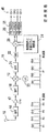
従来技術の基地局は、通常、連続する周波数スペクトルを収束する複数のキャリアを使用する必要がある。基地局に実施可能な従来技術のスーパーヘテロダイン受信機11のブロック図を図1に示す。オペレータには、通常、2つまたはそれ以上のチャネルCh1〜Ch4(キャリア)が割り当てられ、これらを各セルで使用することが望まれる(周波数の再使用=1)。ある種の制約のためにこれが不可能であり、そのため周波数の再使用ファクタが低くなる場合、オペレータは有限数のチャネルを有し、それらを連続するスペクトルのセクションに区分することになり、いくつかの隣接チャネルが各セルで使用される。この場合、受信機11はすべてのチャネル(キャリア)を同時に処理する必要がある。これにより、ハードウェアのコスト、サイズおよび電力消費が最小化される。
Prior art base stations typically need to use multiple carriers that converge a continuous frequency spectrum. A block diagram of a prior
以前は、基地局受信機の高度に厳しい要件はスーパーヘテロダインアーキテクチャでのみ適合することができた。ダイレクトコンバージョンアーキテクチャは、RF信号を直接ベースバンドにダウンコンバートすることから生じる多くの特有の問題がある。これらの問題には、ベースバンド信号中にDCオフセットを生み出すセルフミキシングと、強い干渉信号をベースバンドに変換する偶数次のひずみと、すべての半導体デバイスに固有であり、周波数(f)に逆比例し、ベースバンド信号をマスクする1/fノイズと、他のユーザに干渉するLO信号のスプリアス放射とが含まれる。ダイレクトコンバージョン受信機は、また、ゲインコントロールおよびフィルタリングをすべてベースバンドで行わなければならないため、アナログベースバンド処理コンポーネントの最先端の能力を要求する。これにより、高ダイナミックレンジおよび広帯域幅を有する高価な増幅器が必要になる。 Previously, the highly stringent requirements of base station receivers could only be met with a superheterodyne architecture. The direct conversion architecture has many unique problems that result from downconverting the RF signal directly to baseband. These problems include self-mixing that creates a DC offset in the baseband signal, even-order distortion that converts strong interference signals to baseband, and is inherent to all semiconductor devices and is inversely proportional to frequency (f) 1 / f noise that masks the baseband signal and spurious emission of the LO signal that interferes with other users. Direct conversion receivers also require the state-of-the-art capabilities of analog baseband processing components because all gain control and filtering must be done in baseband. This requires expensive amplifiers with high dynamic range and wide bandwidth.
従来のマルチキャリア無線機は、図1の受信機に示されるように、中間周波数(IF)およびダイレクトデジタルサンプリングを使用して、複数のキャリアをベースバンドへ、そして複数のキャリアをベースバンドからブロック変換するスーパーヘテロダイン無線アーキテクチャに基づいている。IFは通常、50MHzより上に位置するため、ダイレクトデジタルサンプリングには、100MHzを超えるサンプリングレートが可能であり、非常に低いクロックジッタを必要とするアナログ−デジタル変換器(ADC)およびデジタル−アナログ変換器(DAC)などの、高価な高速またはサブサンプリングのデータ変換器を必要とする。 Conventional multi-carrier radios use intermediate frequency (IF) and direct digital sampling to block multiple carriers to baseband and multiple carriers from baseband, as shown in the receiver of FIG. Based on superheterodyne radio architecture to convert. Because the IF is typically located above 50 MHz, direct digital sampling allows sampling rates in excess of 100 MHz and requires analog to digital converters (ADC) and digital to analog conversion that require very low clock jitter. It requires expensive high speed or sub-sampling data converters such as DACs (DACs).
ダイレクトデジタルサンプリングの他の欠点は、隣接チャネルにおける干渉を除去するために必要なIF表面弾性波(SAW)フィルタである。無線機によってサポートされるキャリアの最大数により、SAWフィルタの帯域幅が決定される。異なる数のキャリアをサポートするためには、追加のSAWフィルタが必要である。代替方法として、対象の帯域全体をカバーする1つのIFフィルタを使用することができるが、追加の干渉に対応するためにADCに追加のダイナミックレンジが必要となる。 Another drawback of direct digital sampling is the IF surface acoustic wave (SAW) filter that is required to remove interference in adjacent channels. The maximum number of carriers supported by the radio determines the bandwidth of the SAW filter. In order to support a different number of carriers, an additional SAW filter is required. As an alternative, one IF filter that covers the entire band of interest can be used, but additional dynamic range is required in the ADC to accommodate the additional interference.
これは、受信信号のダイナミックレンジから理解することができる。アップリンクチャネルがすべて同一基地局の制御下にある場合、無線周波数(RF)キャリアは同じようなパワーレベルで受信されることになり、ADCでの必要なダイナミックレンジは比較的小さくてよい。しかしながら、IFフィルタの帯域幅が帯域全体をカバーする場合、他の基地局に属するアップリンクチャネルがADCの入力に現れることになる。これらのチャネルはレベルが非常に高くなる場合があり、ADCでの必要なダイナミックレンジがより大きくなる。 This can be understood from the dynamic range of the received signal. If all uplink channels are under the control of the same base station, radio frequency (RF) carriers will be received at similar power levels and the required dynamic range at the ADC may be relatively small. However, if the IF filter bandwidth covers the entire band, uplink channels belonging to other base stations will appear at the input of the ADC. These channels can be very high in level and require a greater dynamic range at the ADC.
改めて図1を参照すると、受信機11は、たとえば符号分割多元接続(CDMA)通信などのデジタルマルチキャリア無線通信に使用される。信号がアンテナ15で受信されると、第1のバンドパスフィルタ16および線形増幅器17を通過する。第2のバンドパスフィルタ18は増幅器17から信号を受け取り、この信号をミキサ19に提供する。ローカル発振器20がミキサ19に接続されており、ミキサ19は信号をRFからIFに変換し、その後バンドパスフィルタ21によってフィルタされる。
Referring back to FIG. 1, the
バンドパスフィルタ21はADC22に接続され、そのデジタル化された出力がデジタルダウンコンバータ23に提供される。複素数的に数値制御された発振器24を使用して、デジタルダウンコンバータ23を制御し、IFの各チャネルをベースバンドに変換する。デジタルダウンコンバータ23は、直交ベースバンド信号を有限インパルス応答(FIR)フィルタ25のバンクに提供し、これによりパルス整形および干渉除去を行う。FIRフィルタ25からの出力は、それぞれのデジタル自動ゲインコントロール回路(DAGC)35に提供され、このDAGCは4つのそれぞれのチャネル45に出力を提供する。各チャネルからのデジタルデータは、データの復調および復号などの更なる処理のために、デジタルプロセッサ(図示せず)に送られる。一例として4つのチャネルが示されているが、当業者であればいくつのチャネルでも可能であることを理解されよう。
The
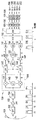
図2に示すように、送信側でも同様のプロセスが使用され、図2は4つの入力チャネルCh1〜Ch4 65を使用する従来技術の送信機51を示すブロック図である。4つの入力チャネル65がそれぞれのパワーコントロール回路75に提供され、次にその出力がそれぞれのFIRフィルタ85に提供される。FIRフィルタ85は、通常、パルス整形のために使用される。FIRフィルタ85からの出力はデジタルアップコンバータ95に直交して提供され、このコンバータは複素数的に数値制御された発振器96に接続される。デジタルアップコンバータ95の出力はデジタル−アナログ(DAC)回路97に提供され、このDACはそのアナログ出力を第1のバンドパスフィルタ98に供給し、次にこれがIFミキサ99に提供される。IFミキサ99はそのローカル発振器信号を発振器100から受け取り、出力を第2のバンドパスフィルタ102に提供する。この出力バンドパスフィルタは増幅器103で増幅され、出力バンドパスフィルタ104でフィルタされて、アンテナ105経由での送信のために提供される。
As shown in FIG. 2, a similar process is used on the transmitting side, and FIG. 2 is a block diagram illustrating a prior art transmitter 51 that uses four input channels Ch1-Ch466. Four
これらの構成(図1および図2)では、様々な変換がRFコンポーネントで行われる。これらのRFコンポーネントの製造コストはかなりなものである。それゆえ、実用上最大限、複数のRF変換を避ける回路を提供することが有利であろう。さらに、受信機および送信機のためのダイレクトコンバージョン設計が望ましい。 In these configurations (FIGS. 1 and 2), various conversions are performed at the RF component. The cost of manufacturing these RF components is considerable. Therefore, it would be advantageous to provide a circuit that avoids multiple RF conversions to the maximum practically. In addition, direct conversion designs for receivers and transmitters are desirable.
従来技術のダイレクトコンバージョン受信機に付随する主な問題は、受信機の出力におけるDCオフセットの発生である。DCオフセットの主な源は、ローカル発振器のセルフミキシングとミキサの二次相互変調(IP2)である。DCオフセットは、かなり大きくなり、ADCの飽和や受信機の他の性能上の問題につながることがある。 The main problem associated with prior art direct conversion receivers is the occurrence of a DC offset in the output of the receiver. The main sources of DC offset are local oscillator self-mixing and mixer second-order intermodulation (IP2). The DC offset can be quite large, leading to ADC saturation and other performance issues in the receiver.
ダイレクトコンバージョンの問題に対する解決策はかねてから理解されてきたが、近年の技術開発により、モノリシックRF集積回路(RFIC)上での集積ソリューションが可能になるまでは、実用的でないかまたは費用効果が低かった。これらの問題に対する解決策には、偶数次のひずみをなくすバランス型(差動)構造、低い1/fノイズおよび優れた線形性を示すSiGe半導体技術、ならびにセルフミキシングおよびLOスプリアス放射をなくすハーモニックミキシングが含まれる。広帯域無線技術への移行によって、ダイレクトコンバージョン受信機のノイズフロア全体に対する1/fノイズの寄与も削減された。さらに、現在では、高速で高線形性の増幅器がアナログベースバンド処理要件を満たすために利用可能である。 Solutions to the direct conversion problem have been understood for some time, but until recent technology developments enabled integrated solutions on monolithic RF integrated circuits (RFICs), it was not practical or cost effective . Solutions to these problems include balanced (differential) structures that eliminate even-order distortion, SiGe semiconductor technology that exhibits low 1 / f noise and excellent linearity, and harmonic mixing that eliminates self-mixing and LO spurious emissions. Is included. The shift to broadband wireless technology has also reduced the contribution of 1 / f noise to the overall noise floor of direct conversion receivers. In addition, high speed, high linearity amplifiers are now available to meet analog baseband processing requirements.
しかし、受信機の出力でのDCオフセットの発生において、ダイレクトコンバージョン受信機に付随する主な問題が依然として存在する。DCオフセットの主な源は、LOセルフミキシングおよびミキサの二次相互変調である。DCオフセットは、かなり大きくなる場合があり、ADCの飽和および受信機の他の性能上の問題につながる。したがって、従来技術は進歩しているものの、これら従来技術の技法は依然として最適な性能に遠く及ばない。 However, the main problem associated with direct conversion receivers still exists in the occurrence of DC offset at the output of the receiver. The main sources of DC offset are LO self-mixing and mixer second order intermodulation. The DC offset can be quite large, leading to ADC saturation and other performance problems of the receiver. Thus, although the prior art has progressed, these prior art techniques still do not go far to optimal performance.
本発明は、ダイレクトコンバージョンのマルチキャリアプロセッサを含む、受信機、送信機または送受信機などの無線通信デバイスである。マルチキャリアプロセッサは、直交変調器(送信機)または復調器(受信機)を用いて、RFチャネルをベースバンドへ、そしてRFチャネルをベースバンドから周波数変換する。アナログ信号はDC近辺に変換されるので、従来の調整可能なフィルタは帯域幅コントロールユニットを介して、異なる数のチャネル(キャリア)およびチャネル帯域幅をサポートするようにプログラムすることができる。 The present invention is a wireless communication device such as a receiver, transmitter, or transceiver that includes a direct conversion multi-carrier processor. The multi-carrier processor uses an orthogonal modulator (transmitter) or demodulator (receiver) to frequency convert the RF channel to baseband and the RF channel from baseband. Since the analog signal is converted to near DC, conventional tunable filters can be programmed to support different numbers of channels (carriers) and channel bandwidths via the bandwidth control unit.
本発明について、全体を通じて同様の番号が同様の要素を表す図面を参照しながら説明する。 The present invention will be described with reference to the drawings, wherein like numerals represent like elements throughout.
本発明は、ダイレクトコンバージョン送信機/受信機およびベースバンド信号処理を用いた無線通信システムにおいて、複数のRFキャリアのブロック処理を可能にする。このようなマルチキャリア無線機は、別個の無線機でそれぞれのキャリアを処理するのではなく、単一の無線機内で複数のキャリアを同時に処理することによって、コストを削減する。 The present invention enables block processing of multiple RF carriers in a wireless communication system using direct conversion transmitter / receiver and baseband signal processing. Such multi-carrier radios reduce costs by processing multiple carriers simultaneously within a single radio, rather than processing each carrier with a separate radio.
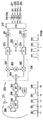
図3は、本発明に従って構築された通信受信機130の例示的な実施形態を示すブロック図である。受信機130は、それぞれがキャリア周波数F1、F2...Fnを介してそれぞれ送信される複数の通信信号Ch1、Ch2...Chnを受信する。これらの信号は、以下ではまとめてマルチキャリア信号S1と呼ぶことにする。
FIG. 3 is a block diagram illustrating an exemplary embodiment of a
受信機130は、アンテナ131、第1のバンドパスフィルタ132、無線周波数増幅器133、および第2のバンドパスフィルタ134を有する。さらに、ローカル発振器143に接続された第1および第2のミキサ141、142と、第1および第2のローパスフィルタ(LPF)145、146と、帯域幅コントロール回路147と、第1および第2のベースバンド増幅器151、152とが含まれる。ローカル発振器143に結合された第1および第2のミキサ141、142は、復調器144を構成する。
The
第1の自動ゲインコントロール(AGC)回路153はベースバンド増幅器151、152に接続され、ベースバンド増幅器151、152からの出力はADC回路161、162に提供される。ADC161、162からのデジタル化された出力は、第2のAGC回路163に提供される。第2のAGC回路163は、AGC出力をDAC164に提供し、次にこのDACは第1のAGC回路153に入力を提供し、これによってベースバンド増幅器151、152の利得を制御する。
A first automatic gain control (AGC)
第2のAGC回路163からの出力は、デジタルダウンコンバータ171に提供され、このダウンコンバータは別々の出力を複数のFIRフィルタ181〜185に、次に複数のDAGC191〜195に提供して、複数のチャネルCh1〜Chn198〜202に出力を提供する。デジタル−アナログAGCループ163、164、153を使用することによって、出力でのダイナミックレンジが削減され、それゆえデジタルAGC回路191〜194ダウンストリームの必要なダイナミックレンジが削減される。
The output from the
アンテナ131はマルチキャリア信号S1を捕捉し、信号S1をバンドパスフィルタ132に入力し、このフィルタが帯域フィルタリングを提供して帯域外の干渉を除去する。フィルタリング後、信号は受信機130のノイズフロアを設定する低ノイズ増幅器(LNA)133に入力される。LNA133の出力はバンドパスフィルタ(BPF)134を通じてフィルタされ、LNA133によって生成された任意の相互変調ひずみをフィルタする。
The
LNA133の出力は、ミキサ141および143ならびに安定なローカル発振器(LO)143からなる復調器144に送られる。LO143は、キャリアに対して1つは同相(I)であり1つは直交(Q)である2つの出力を有する。LO143の周波数は入力チャネルCh1〜Chnの中心周波数、(F1−Fn)/2であり、F1は第1のチャネルCh1のキャリア周波数であり、Fnはn番目のチャネルChnのキャリア周波数である。復調器144は、所望の信号をDC付近の信号を中心としてRFからベースバンドに変換する。
The output of the
IおよびQ信号はLPF145および146に送られ、これらによりダウンストリームベースバンド処理エレメント151〜194のダイナミックレンジを最小にするために、干渉除去が提供される。アナログ信号はDC近辺に変換されるので、従来の調整可能なフィルタ145および146は、異なるチャネル数およびチャネル帯域幅をサポートするように帯域幅コントロール147を介してプログラムすることができる。
The I and Q signals are sent to LPFs 145 and 146, which provide interference cancellation to minimize the dynamic range of downstream baseband processing elements 151-194. Since the analog signal is converted to near DC, conventional
ADC161、162は、復調器144からのI/Q信号をデジタル化する従来の低コストADCのペアである。個々のチャネルCh1〜Chnが、DDC171によってベースバンドにダウンコンバートされる。
チャネルフィルタリングおよびパルス整形は、FIRフィルタ181〜185によって各チャネルCh1〜Chnに適用される。 Channel filtering and pulse shaping are applied to each channel Ch 1 -Ch n by FIR filters 181-185.
AGCプロセスは2つのステップで行われる。第1のステップは第1および第2のAGC回路151、163で行われて、信号をADC161、162のダイナミックレンジ内に維持するようにベースバンド増幅器151、152のゲインを調整する。AGCプロセスの第2のステップは、DAGCブロック191〜195においてデジタル的に行われ、I/Q信号のビット幅を各チャネル198〜202の必要最低限に低減するために使われる。
The AGC process is performed in two steps. The first step is performed by the first and
図3に示されるように、受信機130はマルチキャリアダイレクトコンバージョン受信機として動作する。複数のRFチャネルを含む周波数ブロックは、これによって周波数のブロックとしてベースバンドに直接ダウンコンバートされる。
As shown in FIG. 3, the
図4は、本発明に従って構築されたダイレクトコンバージョン通信送信機230の例示的な実施形態を示すブロック図である。個々のチャネル(Ch1〜Chn)231〜234は先ずFIRフィルタ241〜244を介して送られ、デジタルアップコンバータDUC247によってデジタル的にアップコンバートされる。これによってデジタルベースバンド信号が提供され、この信号は低コストのDACペア251、252を駆動するために使用される。DUC247は、中心周波数をゼロから帯域幅の+/−半分にシフトすることによって、入力信号をI/Q信号成分に変換する。
FIG. 4 is a block diagram illustrating an exemplary embodiment of a direct
DUC247の出力は、直交成分に分かれた2つのデジタル出力を備える。これらのI/Q出力はDAC251および252に入力され、これらDACがデジタル信号をアナログに変換する。DAC251、252からのアナログ出力はLPF253、254に提供され、その帯域幅は帯域幅コントロール回路255によって制御される。LPF253、254はアナログ信号をフィルタして、それらそれぞれのフィルタ出力を、2つのミキサ261、262、LO263および加算器264を備える変調器260に提供する。ミキサ261、262はLO263によって制御され、混合出力を加算器264に提供する。変調器260は出力をバンドパスフィルタ265に、次に第1のRF増幅器266に提供する。RF増幅器266はゲインコントロール回路267によって制御され、出力をバンドパスフィルタ268に、さらにRFパワー増幅器269に提供し、この増幅器はアンテナ270経由での送信のために信号を増幅する。
The output of the
図3および4で明らかに分かるように、本発明に従ったダイレクトコンバージョンマルチキャリアプロセッサは、IFステージをなくすことによってスーパーヘテロダイン無線機の欠点を回避する。これによって無線機でのコストが削減され、データコンバータがベースバンドで低クロックレートで動作できるようにし、これによってさらにコストが削減される。調整可能な帯域幅フィルタはベースバンドで容易に実現可能であり、無線機内で処理される可変のキャリア間隔およびキャリアの数を柔軟にサポートすることができる。これによって所望のキャリアのみがADCに存在することになるので、ADCで要求されるダイナミックレンジも小さくなり、さらにコストが削減される。 As clearly seen in FIGS. 3 and 4, the direct conversion multi-carrier processor according to the present invention avoids the disadvantages of superheterodyne radios by eliminating the IF stage. This reduces the cost at the radio and enables the data converter to operate at a low clock rate in baseband, thereby further reducing the cost. Adjustable bandwidth filters can be easily implemented in baseband and can flexibly support variable carrier spacing and number of carriers processed in the radio. As a result, only the desired carrier is present in the ADC, so the dynamic range required by the ADC is also reduced, and the cost is further reduced.
本発明は、無線ローカルループ、無線LANアプリケーション、ならびにWCDMA(UTRATDDおよびUTRAFDD双方)、TDSCDMA、CDMA2000、3xRTおよびOFDMAシステムなどのセルラシステムを含む無線通信システムに適用可能である。 The present invention is applicable to wireless local loops, wireless LAN applications, and wireless communication systems including cellular systems such as WCDMA (both UTRADDD and UTRAFDD), TDSCDMA, CDMA2000, 3xRT and OFDMA systems.
本発明について好ましい実施形態に関して説明してきたが、当業者であれば、添付の特許請求の範囲に画定される本発明の範囲内にある他の変形形態についても明らかとなるであろう。 While the invention has been described in terms of preferred embodiments, those skilled in the art will recognize other variations that are within the scope of the invention as defined by the appended claims.
Claims (10)
マルチキャリアRF信号を受信するためのアンテナと、
前記アンテナと復調器との間のインターフェースを提供するRF増幅器であって、前記受信したマルチキャリアRF信号を増幅するように構成されたRF増幅器と、
前記マルチキャリアRF信号を同相(I)および直交(Q)のベースバンド信号に変換するように構成され、前記RF増幅器に結合された復調器と、
第1および第2のベースバンドステージであって、各ステージがローパスフィルタおよび選択的に制御可能な増幅器を備え、前記第1のステージがIベースバンド信号を処理するように構成され、前記第2のステージがQベースバンド信号を処理するように構成された第1および第2のベースバンドステージと、
第1および第2のアナログ−デジタル変換器であって、前記第1の変換器が前記Iベースバンド信号をデジタルのI信号に変換するように構成され、前記第2の変換器が前記Qベースバンド信号をデジタルのQ信号に変換するように構成され、前記選択的に制御可能な増幅器の利得が前記デジタルのIおよびQ信号の信号レベルに一部基づいて制御される、第1および第2のアナログ−デジタル変換器と、
前記アナログ−デジタル変換器に接続されたダイレクトコンバージョン回路であって、前記デジタルのIおよびQ信号を複数のチャネル信号に変換するためのダイレクトコンバージョン回路と、
前記ダイレクトコンバージョン回路に接続されたデジタルAGCブロックであって、前記デジタルのIおよびQ信号のビット幅を各チャンネルに必要な最小値に低減するように構成されたデジタルAGCブロックと
を備えたことを特徴とする受信機。A multi-carrier direct conversion receiver for receiving and processing a multi-carrier radio frequency (RF) signal,
An antenna for receiving a multi-carrier RF signal;
An RF amplifier providing an interface between the antenna and a demodulator, the RF amplifier configured to amplify the received multi-carrier RF signal;
A demodulator configured to convert the multi-carrier RF signal into in-phase (I) and quadrature (Q) baseband signals and coupled to the RF amplifier;
First and second baseband stages, each stage comprising a low pass filter and a selectively controllable amplifier, wherein the first stage is configured to process an I baseband signal; First and second baseband stages configured to process Q baseband signals;
First and second analog-to-digital converters, wherein the first converter is configured to convert the I baseband signal to a digital I signal, and the second converter is the Q base First and second configured to convert a band signal into a digital Q signal, wherein the gain of the selectively controllable amplifier is controlled based in part on the signal level of the digital I and Q signals An analog-to-digital converter,
A direct conversion circuit connected to the analog-to-digital converter, the direct conversion circuit for converting the digital I and Q signals into a plurality of channel signals ;
A digital AGC block connected to the direct conversion circuit, the digital AGC block configured to reduce the bit width of the digital I and Q signals to a minimum value necessary for each channel ; Features receiver.
前記複数のチャネル信号を受信し、前記複数のチャネル信号に対応するデジタルの同相(I)信号および前記複数のチャネル信号に対応するデジタルの直交(Q)信号を出力するように構成されたデジタルアップコンバータと、
第1および第2のデジタル−アナログ変換器であって、前記第1の変換器が前記デジタルのI信号をベースバンド周波数のアナログのI信号に変換するように構成され、前記第2の変換器が前記デジタルのQ信号をベースバンド周波数のアナログのQ信号に変換するように構成された第1および第2のデジタル−アナログ変換器と、
前記アナログのベースバンドIおよびQ信号を変調して、合成された無線周波数(RF)信号を提供するように構成された変調器と、
前記RF信号を送信するように構成された送信デバイスと、
複数の有限インパルス応答(FIR)フィルタであって、各フィルタが前記複数のチャネル信号の1つを受信し、前記デジタルアップコンバータにそれぞれのチャネル信号のフィルタ出力を提供するように構成された複数のFIRフィルタと
を備えたことを特徴とする送信機。A multi-carrier direct modulation transmitter for processing and transmitting a plurality of channel signals,
Digital up configured to receive the plurality of channel signals and output a digital in-phase (I) signal corresponding to the plurality of channel signals and a digital quadrature (Q) signal corresponding to the plurality of channel signals A converter,
First and second digital-to-analog converters, wherein the first converter is configured to convert the digital I signal to an analog I signal at a baseband frequency; and the second converter First and second digital-to-analog converters configured to convert the digital Q signal to an analog Q signal at baseband frequency;
A modulator configured to modulate the analog baseband I and Q signals to provide a combined radio frequency (RF) signal;
A transmitting device configured to transmit the RF signal;
A plurality of finite impulse response (FIR) filters, each filter configured to receive one of the plurality of channel signals and provide a filter output of the respective channel signal to the digital upconverter. A transmitter comprising: an FIR filter .
Applications Claiming Priority (2)
| Application Number | Priority Date | Filing Date | Title |
|---|---|---|---|
| US38720702P | 2002-06-07 | 2002-06-07 | |
| PCT/US2003/017851 WO2003105390A2 (en) | 2002-06-07 | 2003-06-05 | System and method for a direct conversion multi-carrier processor |
Publications (2)
| Publication Number | Publication Date |
|---|---|
| JP2005529544A JP2005529544A (en) | 2005-09-29 |
| JP4152944B2 true JP4152944B2 (en) | 2008-09-17 |
Family
ID=29736279
Family Applications (1)
| Application Number | Title | Priority Date | Filing Date |
|---|---|---|---|
| JP2004512332A Expired - Fee Related JP4152944B2 (en) | 2002-06-07 | 2003-06-05 | System and method for direct conversion multi-carrier processor |
Country Status (12)
| Country | Link |
|---|---|
| US (2) | US7162218B2 (en) |
| EP (2) | EP1522151B1 (en) |
| JP (1) | JP4152944B2 (en) |
| KR (3) | KR20050096208A (en) |
| CN (2) | CN100426690C (en) |
| AR (1) | AR040160A1 (en) |
| AU (1) | AU2003238923A1 (en) |
| CA (1) | CA2488740A1 (en) |
| MX (1) | MXPA04012249A (en) |
| NO (1) | NO20045559L (en) |
| TW (3) | TW200715777A (en) |
| WO (1) | WO2003105390A2 (en) |
Families Citing this family (39)
| Publication number | Priority date | Publication date | Assignee | Title |
|---|---|---|---|---|
| DE60111056T2 (en) * | 2001-10-26 | 2006-05-04 | Stmicroelectronics N.V. | Direct match receiver for a non-constant envelope communication system |
| DE10253671B3 (en) * | 2002-11-18 | 2004-08-19 | Infineon Technologies Ag | Suppression of adjacent channel interference through adaptive channel filtering in mobile radio receivers |
| DE60239349D1 (en) * | 2002-12-18 | 2011-04-14 | Texas Instruments Inc | Message receiver with automatic gain control |
| US7995684B2 (en) * | 2003-02-01 | 2011-08-09 | Qualcomm, Incorporated | Method and apparatus for automatic gain control of a multi-carrier signal in a communication receiver |
| US20050053127A1 (en) * | 2003-07-09 | 2005-03-10 | Muh-Tian Shiue | Equalizing device and method |
| US7869528B2 (en) * | 2003-10-31 | 2011-01-11 | Northrop Grumman Systems Corporation | Multi-carrier transceiver assembly |
| US7664520B2 (en) * | 2004-06-24 | 2010-02-16 | Nokia Corporation | Low current direct conversion transmitter architecture |
| JP4708076B2 (en) * | 2005-04-14 | 2011-06-22 | 三星電子株式会社 | Down converter and up converter |
| US8000302B2 (en) | 2005-06-23 | 2011-08-16 | Qualcomm Incorporated | Adaptive multi-channel modem |
| US7477879B1 (en) * | 2005-06-30 | 2009-01-13 | Silicon Laboratories, Inc. | Transceiver system with common receiver and transmitter oscillator |
| US8295371B2 (en) * | 2006-07-14 | 2012-10-23 | Qualcomm Incorporated | Multi-carrier receiver for wireless communication |
| US8693525B2 (en) * | 2006-07-14 | 2014-04-08 | Qualcomm Incorporated | Multi-carrier transmitter for wireless communication |
| WO2008044868A1 (en) * | 2006-10-11 | 2008-04-17 | Electronics And Telecommunications Research Institute | Receiver and receiving method for scalable bandwidth |
| KR100789784B1 (en) * | 2006-10-11 | 2007-12-28 | 한국전자통신연구원 | Receiver and receiving method for scalable bandwidth |
| US7826815B2 (en) * | 2007-07-13 | 2010-11-02 | Fairchild Semiconductor Corporation | Dynamic selection of oscillation signal frequency for power converter |
| US7945217B2 (en) * | 2007-11-13 | 2011-05-17 | Provigent Ltd. | Multi-mode baseband-IF converter |
| FI20075958A0 (en) | 2007-12-21 | 2007-12-21 | Nokia Corp | Processing of broadcast signals in a radio transmitter |
| US7991368B2 (en) * | 2007-12-27 | 2011-08-02 | Provigent Ltd | Integrated RF-IF converter |
| GB2458908B (en) * | 2008-04-01 | 2010-02-24 | Michael Frank Castle | Low power signal processor |
| WO2010013091A1 (en) * | 2008-07-28 | 2010-02-04 | Freescale Semiconductor, Inc. | Semiconductor device wireless communication unit and method for receiving a signal |
| US20100118923A1 (en) * | 2008-11-11 | 2010-05-13 | Debajyoti Pal | Programmable wide band digital receiver/transmitter |
| US8514982B2 (en) * | 2008-12-12 | 2013-08-20 | CSR Technology, Inc | Systems and methods for digitizing multiple channels in a receiver |
| EP2290828B1 (en) | 2009-09-01 | 2016-11-09 | Electronics and Telecommunications Research Institute | Receiving apparatus and receiving method |
| KR101489964B1 (en) * | 2009-09-01 | 2015-02-06 | 한국전자통신연구원 | Receiving apparatus and receiving method |
| US20110053536A1 (en) * | 2009-09-03 | 2011-03-03 | Provigent Ltd | Receiver with re-demodulation |
| US8547207B2 (en) | 2010-03-11 | 2013-10-01 | Checkpoint System, Inc. | RFID converter module |
| DE102010027566A1 (en) * | 2010-05-18 | 2011-11-24 | Rohde & Schwarz Gmbh & Co. Kg | Signal generator with digital intermediate frequency and digital fine tuning |
| US8903330B2 (en) | 2010-12-13 | 2014-12-02 | Huawei Technologies Co., Ltd. | Communication signal transmission method, device and system |
| CN102104392B (en) | 2010-12-15 | 2013-10-09 | 华为技术有限公司 | Multi-band multi-channel transceiving device and method as well as base station system |
| US8406709B2 (en) | 2011-02-27 | 2013-03-26 | Provigent Ltd. | Carrier recovery in re-modulation communication systems |
| US9210009B2 (en) * | 2011-09-15 | 2015-12-08 | Intel Corporation | Digital pre-distortion filter system and method |
| EP2573997A1 (en) * | 2011-09-26 | 2013-03-27 | Thomson Licensing | Method for controlling bandwidth and corresponding device |
| GB2504973B (en) * | 2012-08-15 | 2014-11-19 | Broadcom Corp | Receiver circuit |
| KR101367236B1 (en) * | 2013-06-24 | 2014-02-26 | 주식회사 삼정솔루션 | Apparatus for protecting signal |
| CN105048966A (en) * | 2015-06-12 | 2015-11-11 | 中国电子科技集团公司第四十一研究所 | Multi-phase digital down conversion method for GHz high-speed sampling signal |
| US10191454B2 (en) * | 2016-06-13 | 2019-01-29 | William Marsh Rice University | Methods and related systems of ultra-short pulse detection |
| EP3746385A4 (en) | 2018-02-02 | 2021-10-27 | ATS Automation Tooling Systems Inc. | Linear motor conveyor system for clean/aseptic environments |
| CN113454939B (en) * | 2019-04-30 | 2023-03-03 | 华为技术有限公司 | Method and related device for sending sounding reference signal |
| KR102426630B1 (en) * | 2022-04-12 | 2022-07-28 | 한화시스템(주) | RF signal processing device and method for low orbit satellite |
Family Cites Families (35)
| Publication number | Priority date | Publication date | Assignee | Title |
|---|---|---|---|---|
| US4654800A (en) * | 1984-02-20 | 1987-03-31 | Kabushikikaisha Nippon Coinco | Control and monitoring apparatus for vending machines |
| US5095536A (en) * | 1990-03-23 | 1992-03-10 | Rockwell International Corporation | Direct conversion receiver with tri-phase architecture |
| KR970007983B1 (en) * | 1992-06-08 | 1997-05-19 | 모토로라 인코포레이티드 | Receiver automatic gain control |
| FR2707063B1 (en) * | 1993-06-25 | 1995-09-22 | Alcatel Mobile Comm France | |
| US5519732A (en) * | 1994-05-02 | 1996-05-21 | Harris Corporation | Digital baseband to IF conversion in cellular base stations |
| JPH0832464A (en) * | 1994-07-15 | 1996-02-02 | Uniden Corp | Carrier leak correction method in transmitter |
| US5715314A (en) * | 1994-10-24 | 1998-02-03 | Open Market, Inc. | Network sales system |
| US5758257A (en) * | 1994-11-29 | 1998-05-26 | Herz; Frederick | System and method for scheduling broadcast of and access to video programs and other data using customer profiles |
| US5579341A (en) * | 1994-12-29 | 1996-11-26 | Motorola, Inc. | Multi-channel digital transceiver and method |
| US7937312B1 (en) * | 1995-04-26 | 2011-05-03 | Ebay Inc. | Facilitating electronic commerce transactions through binding offers |
| US6009130A (en) * | 1995-12-28 | 1999-12-28 | Motorola, Inc. | Multiple access digital transmitter and receiver |
| FI112133B (en) * | 1996-03-29 | 2003-10-31 | Nokia Corp | Method of forming the frequencies of a direct conversion transmitter / receiver operating in two different frequency ranges and a direct conversion transmitter / receiver of a radio communication system operating in two different frequency ranges and using the foregoing in a mobile telephone |
| KR0164419B1 (en) * | 1996-04-19 | 1999-02-01 | 김광호 | Agc circuits for radio receiver |
| US5898912A (en) * | 1996-07-01 | 1999-04-27 | Motorola, Inc. | Direct current (DC) offset compensation method and apparatus |
| US6005894A (en) * | 1997-04-04 | 1999-12-21 | Kumar; Derek D. | AM-compatible digital broadcasting method and system |
| US6029052A (en) * | 1997-07-01 | 2000-02-22 | Telefonaktiebolaget Lm Ericsson | Multiple-mode direct conversion receiver |
| IT1294284B1 (en) * | 1997-07-29 | 1999-03-24 | Italtel Spa | WIDE BAND RADIO TRANSMITTER FOR A SIGNAL CONSTITUTED BY A PLURALITY OF EQUIPPED DIGITALLY MODULATED CARRIERS |
| IT1297278B1 (en) | 1997-09-15 | 1999-08-09 | Italtel Spa | WIDE BAND DIGITAL RADIO RECEIVER FOR MULTIPORTANT SIGNAL |
| AUPP261898A0 (en) * | 1998-03-27 | 1998-04-23 | Victoria University Of Technology | Dc offset and im2 removal in direct conversion receivers |
| ATE224119T1 (en) * | 1998-04-14 | 2002-09-15 | Fraunhofer Ges Forschung | METHOD AND DEVICE FOR FINE FREQUENCY SYNCHRONIZATION IN MULTI CARRIER DEMODULATION SYSTEMS |
| JP3319422B2 (en) * | 1998-05-08 | 2002-09-03 | 日本電気株式会社 | Multi-carrier transmission system and multi-carrier transmission method |
| US7106689B1 (en) * | 1999-03-02 | 2006-09-12 | Matsushita Electric Industrial Co., Ltd. | OFDM transmission/reception apparatus |
| US7149726B1 (en) * | 1999-06-01 | 2006-12-12 | Stamps.Com | Online value bearing item printing |
| JP3551841B2 (en) * | 1999-06-09 | 2004-08-11 | 日本電気株式会社 | Receiver and gain control method thereof |
| US6480528B1 (en) * | 1999-06-11 | 2002-11-12 | Qualcomm Incorporated | Automatic gain control for improved decoding of multi-carrier signal |
| US6631170B1 (en) * | 1999-12-03 | 2003-10-07 | Nokia Corporation | Radio frequency receiver |
| US7213005B2 (en) * | 1999-12-09 | 2007-05-01 | International Business Machines Corporation | Digital content distribution using web broadcasting services |
| JP4652546B2 (en) * | 2000-09-21 | 2011-03-16 | 三星電子株式会社 | Receiving machine |
| US6560448B1 (en) * | 2000-10-02 | 2003-05-06 | Intersil Americas Inc. | DC compensation system for a wireless communication device configured in a zero intermediate frequency architecture |
| WO2002069443A1 (en) * | 2001-02-28 | 2002-09-06 | Itt Manufacturing Enterprises, Inc. | Integrated beamformer/method architecture |
| US20020127982A1 (en) * | 2001-03-07 | 2002-09-12 | Nokia Mobile Phones Ltd | Mobile station receiver operable for both single and multi-carrier reception |
| KR100446540B1 (en) * | 2001-04-16 | 2004-09-01 | 삼성전자주식회사 | Transmitter for a data communication |
| US7243153B2 (en) * | 2001-06-26 | 2007-07-10 | Eastman Kodak Company | System and method for managing images over a communication network |
| US20030078011A1 (en) * | 2001-10-18 | 2003-04-24 | Integrated Programmable Communications, Inc. | Method for integrating a plurality of radio systems in a unified transceiver structure and the device of the same |
| US6819910B2 (en) * | 2002-03-08 | 2004-11-16 | Broadcom Corp. | Radio employing a self calibrating transmitter with reuse of receiver circuitry |
-
2003
- 2003-06-05 EP EP03734443.9A patent/EP1522151B1/en not_active Expired - Lifetime
- 2003-06-05 KR KR1020057017487A patent/KR20050096208A/en not_active Application Discontinuation
- 2003-06-05 JP JP2004512332A patent/JP4152944B2/en not_active Expired - Fee Related
- 2003-06-05 KR KR1020047019912A patent/KR100671364B1/en not_active IP Right Cessation
- 2003-06-05 KR KR1020087013473A patent/KR20080059339A/en not_active Application Discontinuation
- 2003-06-05 TW TW095119778A patent/TW200715777A/en unknown
- 2003-06-05 TW TW093104385A patent/TWI320637B/en not_active IP Right Cessation
- 2003-06-05 TW TW092115312A patent/TWI237450B/en not_active IP Right Cessation
- 2003-06-05 MX MXPA04012249A patent/MXPA04012249A/en active IP Right Grant
- 2003-06-05 CN CNB038131463A patent/CN100426690C/en not_active Expired - Fee Related
- 2003-06-05 WO PCT/US2003/017851 patent/WO2003105390A2/en active Application Filing
- 2003-06-05 EP EP16154053.9A patent/EP3032755A1/en not_active Withdrawn
- 2003-06-05 AU AU2003238923A patent/AU2003238923A1/en not_active Abandoned
- 2003-06-05 CA CA002488740A patent/CA2488740A1/en not_active Abandoned
- 2003-06-05 CN CNA2008101660484A patent/CN101425811A/en active Pending
- 2003-06-06 AR ARP030102016A patent/AR040160A1/en active IP Right Grant
- 2003-06-06 US US10/456,300 patent/US7162218B2/en active Active
-
2004
- 2004-12-20 NO NO20045559A patent/NO20045559L/en not_active Application Discontinuation
-
2006
- 2006-11-22 US US11/562,802 patent/US20070085718A1/en not_active Abandoned
Also Published As
| Publication number | Publication date |
|---|---|
| TWI237450B (en) | 2005-08-01 |
| US20070085718A1 (en) | 2007-04-19 |
| TW200400700A (en) | 2004-01-01 |
| US7162218B2 (en) | 2007-01-09 |
| AU2003238923A8 (en) | 2003-12-22 |
| JP2005529544A (en) | 2005-09-29 |
| TWI320637B (en) | 2010-02-11 |
| KR20050014850A (en) | 2005-02-07 |
| WO2003105390A3 (en) | 2004-04-01 |
| US20040072547A1 (en) | 2004-04-15 |
| TW200501594A (en) | 2005-01-01 |
| KR20050096208A (en) | 2005-10-05 |
| WO2003105390A2 (en) | 2003-12-18 |
| KR100671364B1 (en) | 2007-01-22 |
| CN101425811A (en) | 2009-05-06 |
| CA2488740A1 (en) | 2003-12-18 |
| KR20080059339A (en) | 2008-06-26 |
| MXPA04012249A (en) | 2005-02-25 |
| AR040160A1 (en) | 2005-03-16 |
| NO20045559L (en) | 2004-12-20 |
| EP1522151A2 (en) | 2005-04-13 |
| TW200715777A (en) | 2007-04-16 |
| AU2003238923A1 (en) | 2003-12-22 |
| CN100426690C (en) | 2008-10-15 |
| CN1706109A (en) | 2005-12-07 |
| EP1522151B1 (en) | 2016-03-23 |
| EP3032755A1 (en) | 2016-06-15 |
| EP1522151A4 (en) | 2006-05-17 |
Similar Documents
| Publication | Publication Date | Title |
|---|---|---|
| JP4152944B2 (en) | System and method for direct conversion multi-carrier processor | |
| KR100954705B1 (en) | Direct conversion receiver | |
| US9929793B2 (en) | Digital repeater having bandpass filtering, adaptive pre-equalization and suppressin of natural oscillation | |
| JP5608939B2 (en) | Receiver, transmitter, feedback device, transceiver, and signal processing method | |
| US7924802B2 (en) | Wireless communication systems and methods | |
| US8224276B2 (en) | Method and arrangement for signal processing in a receiver that can be tuned to different carriers | |
| KR100736057B1 (en) | Dual digital low IF complex receiver | |
| US20180294825A1 (en) | Dynamic bias control | |
| JP4589331B2 (en) | Multimode multiband transceiver | |
| JP2002290367A (en) | Band division demodulation method and ofdm receiver | |
| KR100715205B1 (en) | System and method for digital multi-band transceiver of the wireless communication system | |
| JP2009522837A (en) | A receiver for broadband communication and a method for receiving data frames from a wireless device in a wireless local area network. | |
| JP2006303718A (en) | Receiver and demodulating method | |
| Efstathiou et al. | Enabling components for multi-standard software radio base stations | |
| JOSHI | Software Defined Radio |
Legal Events
| Date | Code | Title | Description |
|---|---|---|---|
| A131 | Notification of reasons for refusal |
Free format text: JAPANESE INTERMEDIATE CODE: A131 Effective date: 20070501 |
|
| A601 | Written request for extension of time |
Free format text: JAPANESE INTERMEDIATE CODE: A601 Effective date: 20070731 |
|
| A602 | Written permission of extension of time |
Free format text: JAPANESE INTERMEDIATE CODE: A602 Effective date: 20070807 |
|
| A601 | Written request for extension of time |
Free format text: JAPANESE INTERMEDIATE CODE: A601 Effective date: 20070903 |
|
| A602 | Written permission of extension of time |
Free format text: JAPANESE INTERMEDIATE CODE: A602 Effective date: 20070910 |
|
| A521 | Request for written amendment filed |
Free format text: JAPANESE INTERMEDIATE CODE: A523 Effective date: 20070928 |
|
| A02 | Decision of refusal |
Free format text: JAPANESE INTERMEDIATE CODE: A02 Effective date: 20080104 |
|
| RD13 | Notification of appointment of power of sub attorney |
Free format text: JAPANESE INTERMEDIATE CODE: A7433 Effective date: 20080404 |
|
| A521 | Request for written amendment filed |
Free format text: JAPANESE INTERMEDIATE CODE: A523 Effective date: 20080501 Free format text: JAPANESE INTERMEDIATE CODE: A821 Effective date: 20080404 |
|
| A911 | Transfer to examiner for re-examination before appeal (zenchi) |
Free format text: JAPANESE INTERMEDIATE CODE: A911 Effective date: 20080514 |
|
| TRDD | Decision of grant or rejection written | ||
| A01 | Written decision to grant a patent or to grant a registration (utility model) |
Free format text: JAPANESE INTERMEDIATE CODE: A01 Effective date: 20080603 |
|
| A01 | Written decision to grant a patent or to grant a registration (utility model) |
Free format text: JAPANESE INTERMEDIATE CODE: A01 |
|
| A61 | First payment of annual fees (during grant procedure) |
Free format text: JAPANESE INTERMEDIATE CODE: A61 Effective date: 20080702 |
|
| R150 | Certificate of patent or registration of utility model |
Free format text: JAPANESE INTERMEDIATE CODE: R150 |
|
| FPAY | Renewal fee payment (event date is renewal date of database) |
Free format text: PAYMENT UNTIL: 20110711 Year of fee payment: 3 |
|
| FPAY | Renewal fee payment (event date is renewal date of database) |
Free format text: PAYMENT UNTIL: 20110711 Year of fee payment: 3 |
|
| FPAY | Renewal fee payment (event date is renewal date of database) |
Free format text: PAYMENT UNTIL: 20120711 Year of fee payment: 4 |
|
| FPAY | Renewal fee payment (event date is renewal date of database) |
Free format text: PAYMENT UNTIL: 20120711 Year of fee payment: 4 |
|
| FPAY | Renewal fee payment (event date is renewal date of database) |
Free format text: PAYMENT UNTIL: 20130711 Year of fee payment: 5 |
|
| R250 | Receipt of annual fees |
Free format text: JAPANESE INTERMEDIATE CODE: R250 |
|
| R250 | Receipt of annual fees |
Free format text: JAPANESE INTERMEDIATE CODE: R250 |
|
| R250 | Receipt of annual fees |
Free format text: JAPANESE INTERMEDIATE CODE: R250 |
|
| R250 | Receipt of annual fees |
Free format text: JAPANESE INTERMEDIATE CODE: R250 |
|
| R250 | Receipt of annual fees |
Free format text: JAPANESE INTERMEDIATE CODE: R250 |
|
| LAPS | Cancellation because of no payment of annual fees |