JP4346697B2 - Imaging device - Google Patents
Imaging device Download PDFInfo
- Publication number
- JP4346697B2 JP4346697B2 JP6289297A JP6289297A JP4346697B2 JP 4346697 B2 JP4346697 B2 JP 4346697B2 JP 6289297 A JP6289297 A JP 6289297A JP 6289297 A JP6289297 A JP 6289297A JP 4346697 B2 JP4346697 B2 JP 4346697B2
- Authority
- JP
- Japan
- Prior art keywords
- image
- circuit
- unit
- signal
- compression
- Prior art date
- Legal status (The legal status is an assumption and is not a legal conclusion. Google has not performed a legal analysis and makes no representation as to the accuracy of the status listed.)
- Expired - Fee Related
Links
Images


Classifications
-
- H—ELECTRICITY
- H04—ELECTRIC COMMUNICATION TECHNIQUE
- H04N—PICTORIAL COMMUNICATION, e.g. TELEVISION
- H04N5/00—Details of television systems
- H04N5/76—Television signal recording
- H04N5/765—Interface circuits between an apparatus for recording and another apparatus
- H04N5/77—Interface circuits between an apparatus for recording and another apparatus between a recording apparatus and a television camera
-
- H—ELECTRICITY
- H04—ELECTRIC COMMUNICATION TECHNIQUE
- H04N—PICTORIAL COMMUNICATION, e.g. TELEVISION
- H04N19/00—Methods or arrangements for coding, decoding, compressing or decompressing digital video signals
- H04N19/60—Methods or arrangements for coding, decoding, compressing or decompressing digital video signals using transform coding
- H04N19/61—Methods or arrangements for coding, decoding, compressing or decompressing digital video signals using transform coding in combination with predictive coding
-
- H—ELECTRICITY
- H04—ELECTRIC COMMUNICATION TECHNIQUE
- H04N—PICTORIAL COMMUNICATION, e.g. TELEVISION
- H04N9/00—Details of colour television systems
- H04N9/79—Processing of colour television signals in connection with recording
- H04N9/80—Transformation of the television signal for recording, e.g. modulation, frequency changing; Inverse transformation for playback
- H04N9/82—Transformation of the television signal for recording, e.g. modulation, frequency changing; Inverse transformation for playback the individual colour picture signal components being recorded simultaneously only
- H04N9/83—Transformation of the television signal for recording, e.g. modulation, frequency changing; Inverse transformation for playback the individual colour picture signal components being recorded simultaneously only the recorded chrominance signal occupying a frequency band under the frequency band of the recorded brightness signal
- H04N9/831—Transformation of the television signal for recording, e.g. modulation, frequency changing; Inverse transformation for playback the individual colour picture signal components being recorded simultaneously only the recorded chrominance signal occupying a frequency band under the frequency band of the recorded brightness signal using intermediate digital signal processing
Description
【0001】
【発明の属する技術分野】
本発明は、画像を撮像する撮像装置(カメラ一体型VTR等)に関するものである。
【0002】
【従来の技術】
従来のカメラ一体型VTRは撮像部と、モニタとVTRとを含む画像表示部とが一体となっていて分離できない構造であった。このため、例えば撮影者の手の届かない場所にカメラ一体型VTRを置いて撮影しようとする場合などでは撮るべき映像をモニタで確認することができないという問題があった。
【0003】
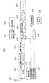
上記の問題を解決するために従来より図14に示すような撮像部と画像表示部とが別体となったカメラ一体型VTRがあった。
図14において、10は撮像部、11は画像表示部である。1は被写体を取り込むレンズ、2は取り込んだ被写体を画像信号に変換する撮像素子、3は上記画像信号をサンプルホールドし、適正な信号レベルにするCDS/AGC回路、4はCDS/AGC回路3からの画像信号をA/D変換し、ディジタル信号処理を行うディジタル信号処理回路、5はディジタル信号処理回路4からのディジタル画像信号をNTSC映像信号に変換するNTSCエンコーダ、6は撮像部10と画像表示部11とを繋ぐケーブル、7は撮像部10又は後述の記録媒体から再生されたNTSC映像信号を表示するモニタ、8は撮像部10からのNTSC映像信号を記録媒体に記録再生するVTR等の記録再生部である。9a、9bは撮像部10と画像表示部11とを機械的に着脱する着脱手段である。
【0004】
上記構成によれば、画像表示部11を撮像部10から離して撮影を行うことができ、また必要に応じて画像表示部11と撮像部10とを着脱手段9a、9bを介して一体化させて使用することができる。
【0005】
【発明が解決しようとする課題】
しかしながら、上記従来例のカメラ一体型VTRは、撮像部からケーブルが延びており、このケーブルが邪魔になって撮影時の自由度を妨げるという問題があった。
【0006】
そこで、本発明は、撮影の自由度を向上させることを目的とする。
【0007】
【課題を解決するための手段】
本発明に係る撮像装置は、画像を表示する表示装置と接続可能な撮像装置であって、撮像手段によって撮像された画像に対応するデジタル画像を第1の圧縮方式に従って圧縮し、第1の圧縮画像を出力する第1の画像圧縮手段と、前記デジタル画像を前記第1の圧縮方式と異なる第2の圧縮方式に従って圧縮し、第2の圧縮画像を出力する第2の画像圧縮手段と、前記表示装置と接続可能であり、前記表示装置が前記撮像装置に接続されている場合に、前記第2の圧縮画像を前記表示装置に供給する接続手段と、前記表示装置が前記撮像装置に接続されていない場合に、前記第1の圧縮画像を前記表示装置に無線で送信する無線送信手段とを有することを特徴とする。
【0011】
【発明の実施の形態】
以下、本発明をカメラ一体型VTRに適用した場合の第1〜5の実施の形態について図面を用いて説明する。尚、図1〜図13において互いに対応する部分には同一番号を付して重複する説明は省略する。
図1は第1の実施の形態によるカメラ一体型VTRの撮像部100を示すブロック図、図2はカメラ一体型VTRの画像表示部200を示すブロック図である。
図1の撮像部100において、101は被写体を取り込むレンズ、102は取り込んだ被写体を画像信号に変換する撮像素子、103は上記画像信号をサンプルホールドし、適正な信号レベルにするCDS/AGC回路、104はCDS/AGC回路103からの画像信号をA/D変換し、ディジタル信号処理を行うディジタル信号処理回路、105はディジタル信号処理回路104からのディジタル画像信号を圧縮符号化する画像圧縮回路、106は画像圧縮回路105からの圧縮画像データをスペクトラム拡散変調して送信するスペクトラム拡散送信部、107は送信アンテナである。
【0012】
108は制御用のマイコン、109は電源、110はマイコン108からの命令によって上記の各回路に送る電源109をON/OFFする電源制御部、112は後述の画像表示部200と合体したことを検知する合体検知装置、113は画像表示部200と合体したときに上記ディジタル信号処理回路104を画像表示部200に接続する信号接続装置、114は合体検知装置112、信号接続装置113を含み画像表示部200と着脱可能に電気的及び機械的に接続する接続手段としての着脱装置である。
【0013】
次に図2の画像表示部200において、201は受信アンテナ、202は撮像部100から送信された画像データを受信し、圧縮画像データを復調するスペクトラム拡散受信部、203は上記圧縮画像データを伸張し、ディジタル画像信号に戻す画像伸張回路、204は上記ディジタル画像信号をNTSC映像信号に変換するNTSCエンコーダ、205は上記NTSC映像信号を記録再生するVTR等の記録再生部、206は記録媒体、207は上記NTSC映像信号を表示するモニタである。
【0014】
208は制御用のマイコン、209は電源、210はマイコン208からの命令によって上記の各回路に送る電源209をON/OFFする電源制御部、211は撮像部100と合体したことを検知する合体検知装置、212は撮像部100と合体したときNTSCエンコーダ204を撮像部100に接続する信号接続装置、213は合体検知装置211、信号接続装置212を含み撮像部100と着脱可能に電気的及び機械的に接続する接続手段としての着脱装置である。
【0015】
なお、上記画像圧縮回路105はディジタル信号処理回路104からのディジタル画像信号を画素単位に処理し、画素を間引いて画素数を減らす画素間引き回路であってよい。また上記画像伸張回路203は、スペクトラム拡散受信部202からのディジタル画像信号を画素単位に処理し、各画素に対して補間する画素補間回路であってよい。
【0016】
上記構成によれば、撮像部100と画像表示部200とが分離している場合には、撮像部100で撮像された映像は無線による通信を介して離れた場所にある画像表示部200まで送られてモニタすることができると共に、さらにその映像を記録再生することもできる。このため、撮影者は画像表示部200の置き場所を考慮することなく撮像部100を離れた場所に設置できるため、撮影の自由度が増す。また、撮像された映像を信号接続装置113から取り出してコンピュータ等の外部装置に送ることもできる。さらに画像表示部200の信号接続装置212に外部装置から画像信号を送り込むことにより、これをモニタしたり、記録再生することもできる。
尚、この場合は合体検知装置112、211が合体状態を検知しないので、マイコン108、208は電源制御部110、210にすべての回路に電源を供給するように命令を出す。
【0017】
一方、撮像部100と画像表示部200とが着脱装置114、213を介して接続され、両者が合体して一体化している場合には、合体検知装置112、211が合体状態を検知し、これに応じてマイコン108、208が電源制御部110、210に、スペクトラム拡散送信部106、スペクトラム拡散受信部202、画像圧縮回路105、画像伸張回路203への電源供給を止めるように命令を出し、上記回路への電源供給が停止される。これにより、合体時の消費電力を減らすことができる。
【0018】
また、両者が分離している場合は、画像信号を圧縮し、データ量を少なくして送信しているので、伝送速度に制限がある電波によるディジタル伝送においても支障なく送信することができる。さらにスペクトラム拡散変調しているので、広い帯域の信号を小電力で伝送することができる。また、両者が一体化している場合には、画像信号を圧縮しないで送信するので、高画質を得ることができる。
【0019】
次に、第2の実施の形態について説明する。
本実施の形態においては、画像圧縮方式としてJPEG圧縮方式とDV圧縮方式とを用いている。ここでJPEG圧縮方式は、画像データの圧縮率を高くすることができるため、伝送速度に制限がある無線伝送路において画像伝送を行うのに適した圧縮方式である。また、パーソナルコンピュータでは、画像データの形式としてJPEG圧縮方式が多く採用されている。
一方、DV圧縮方式は、画像データの圧縮率はあまり高くないが、画質が非常に高品質であるため、ディジタルVTRに多く採用されている。
【0020】
図3は第2の実施の形態による撮像部100を示し、図4は同じく画像表示部200を示す。
【0021】
図3の撮像部100において、115は上記ディジタル信号処理回路104からのディジタル画像信号をJPEG方式で圧縮するJPEG画像圧縮回路、116はディジタル信号処理回路104からのディジタル画像信号をDV方式で圧縮するDV画像圧縮回路、117はマイコン108からの命令によってディジタル信号処理回路104を上記JPEG画像圧縮回路115又は上記DV画像圧縮回路116に接続する圧縮種類選択用のスイッチ、118は上記スイッチ117に連動して切り替わる圧縮種類選択用のスイッチであり、JPEG画像圧縮回路115又はDV画像圧縮回路116を信号接続装置113に切り替え接続する。
【0022】
図4の画像表示部200において、214は上記JPEG圧縮画像データを伸張し、ディジタル画像信号に戻すJPEG画像伸張回路、215はJPEG画像伸張回路214からのディジタル画像信号をDV方式で圧縮するDV画像圧縮回路、216は信号接続装置212からの上記DV圧縮画像データを伸張し、ディジタル画像信号に戻すDV画像伸張回路、217はDV圧縮画像データを記録媒体206にディジタル記録再生するディジタル記録再生部、218はマイコン208からの命令によってディジタル記録再生部217をDV画像圧縮回路215又は信号接続装置212に接続する画像選択用のスイッチである。
【0023】
上記構成において、撮像部100と画像表示部200とが分離している場合には、合体検知装置112、211は合体状態を検知しないので、撮像部100のマイコン108はスイッチ117にディジタル信号処理回路104をJPEG画像圧縮回路115に接続するように命令する。またスイッチ117に連動してスイッチ118は信号接続装置113をJPEG画像圧縮回路115に接続する。一方、画像表示部200のマイコン208は、スイッチ218にディジタル記録再生部217をDV画像圧縮回路215に接続するように命令を出す。
【0024】
このときの信号経路は、記録時には、レンズ101>撮像素子102>CDS/AGC回路103>ディジタル信号処理回路104>スイッチ117>JPEG画像圧縮回路115>スペクトラム拡散送信部106>送信アンテナ107>受信アンテナ201>スペクトラム拡散受信部202>JPEG画像伸張回路214>DV画像圧縮回路215>スイッチ218>ディジタル記録再生部217>記録媒体206、及びJPEG画像伸張回路214>NTSCエンコーダ204>モニタ207となる。
また、信号接続装置113にはJPEG画像圧縮回路115からスイッチ118を介してJPEG圧縮信号が出力されているので、これをコンピュータ等に送ることができる。さらに画像表示部200には信号接続装置212を介して外部からDV圧縮信号を送り込むことができる。
【0025】
再生時には、マイコン208はスイッチ218にディジタル記録再生部217をDV画像伸張回路216に接続するように命令を出す。このときの信号経路は、記録媒体206>ディジタル記録再生部217>スイッチ218>DV画像伸張回路216>NTSCエンコーダ204>モニタ207となる。
【0026】
また、撮像部100と画像表示部200とが合体して一体化している場合には、合体検知装置112、211は合体状態を検知する。撮像部100のマイコン108はスイッチ117にディジタル信号処理回路104をDV画像圧縮回路116に接続するように命令する。またスイッチ117に連動してスイッチ118は信号接続装置113をDV画像圧縮回路116に接続する。一方、画像表示部200のマイコン208は、前記画像選択スイッチ218にディジタル記録再生部217を信号接続装置212に接続するように命令を出す。
【0027】
このときの信号経路は、記録時には、レンズ101>撮像素子102>CDS/AGC回路103>ディジタル信号処理回路104>スイッチ117>DV画像圧縮回路116>スイッチ118>信号接続装置113>信号接続装置212>スイッチ218>ディジタル記録再生部217>記録媒体206、及び信号接続装置212>DV画像伸張回路216>NTSCエンコーダ204>モニタ207となる。
【0028】
また再生時の信号経路は、記録媒体206>ディジタル記録再生部217>スイッチ218>DV画像伸張回路216>NTSCエンコーダ204>モニタ207となる。
【0029】
以上のように本実施の形態では、撮像部100と画像表示部200とが分離している場合は、画像圧縮方式としてJPEG方式が選択されるため、無線通信が有効に行われる。
【0030】
また、撮像部100と画像表示部200とが合体して一体化している場合は、画像圧縮方式としてDV方式が選択されるため、高画質なディジタル画像記録を行うことができる。
【0031】
図5は図3のJPEG画像圧縮回路115の構成を示すブロック図である。
図5において、301はラスターブロック変換部、302はDCT(離散コサイン変換)部、303は量子化部、304はハフマン符号化部、305は上記量子化部303に与えられる量子化テーブル、306は上記ハフマン符号化部304に与えるハフマンテーブルである。
【0032】
上記構成のJPEG画像圧縮回路115において、入力されたラスタ形式の輝度/色差からなるディジタル画像信号は、ラスタ−ブロック変換部301によって8画素×8画素のブロックに分割され、それぞれ8×8の正方行列で表されるデータとなる。次に、DCT変換部302において、上記8×8の行列データにDCT(離散コサイン変換)と呼ばれる変換を行う。変換後のデータはDCT係数と呼ばれ、やはり8×8の行列データであるが、その行列の左上の項は原画像の低周波成分の大きさ、右下の項は原画像の高周波成分の大きさを示す値となっている。
【0033】
続いて量子化部303において、上記行列データのそれぞれに対して、量子化テーブル305と呼ばれる係数テーブルを用いて除算を行う。量子化テーブル305は低周波成分に対して高周波成分に重み付けされており、除算結果は高周波成分になるほど小さい値を示す行列データになる。続いて量子化を行い、一定以下の値を切り捨て、0にする。この結果行列データは、右下の項の値はほとんどが0となる。
【0034】
次に上記行列データをジグザグスキャンと呼ばれる順に一列に並べたデータ列とし、ハフマン符号化部304でハフマン符号化と呼ばれる変換を行う。この変換は、データの冗長部分(同じ値が続くデータ部分)を別の短い符号で表す変換であるので、上記データ列では0が続く部分のデータ列が大幅に短くなり、この結果、画像データ量が圧縮されたことになる。
【0035】
図6は図4のJPEG画像伸張回路214の構成を示すブロック図である。
図6において、401はハフマン復号化部、402は上記ハフマン復号化部401に与えるハフマンテーブル、403は逆量子化部、404は上記逆量子化部403に与えられる量子化テーブル、405は逆DCT変換部、406はブロック−ラスタ変換部である。
【0036】
上記構成のJPEG画像伸張回路214において、入力されたJPEG圧縮画像信号は、ハフマン復号化部401でハフマン復号化され、元のデータ列を得る。次にこのデータ列を行列データに戻し、逆量子化部403で量子化テーブル404を用いて乗算を行う。このとき得られる行列データは、前記DCT係数と比較すると、高周波成分の方で0が多くなっている。次に逆DCT変換部405により逆DCT変換を行い、ブロック−ラスタ変換部406でブロックを元通りに並べることにより、伸張されたディジタル画像を得る。
【0037】
図7は図4のDV画像圧縮回路215の構成を示すもので、ブロック分割シャッフリング回路501、DCT演算重み付け回路502、並べ替え回路503、適応量子化回路504、可変長符号化回路505、デシャッフリング回路506、動き検出回路507、符号量推定回路508で構成されている。
【0038】
上記構成において、伝送速度を変換したデータは、ブロック分割シャッフリング回路501において、輝度信号、2つの色信号のそれぞれを8画素×8画素のブロックに変換し、4つのY信号ブロックと2つの色差信号ブロックをあわせた6ブロックでマクロブロックを構成する。分割したデータは画面上の位置を入れ替えて、固定長にする範囲の情報量を平均化した後、DCT演算重み付け回路502においてDCT(離散コサイン変換)を施す。このとき動きの多い映像はフレーム内で演算する。このために動き検出回路507を備えている。DCTの後、データの重み付けを行い、並べ替え回路503で並べ替えをした後、適応量子化部回路504で量子化する。量子化したデータは可変長符号化回路505で可変長符号化(VLC)を施す。量子化するときに符号量を推定し、可変長符号化した後の符号量がマクロブロック毎に一定になるようにする。符号化したデータは画面上の元位置に戻してから出力する。そして出力されたディジタル信号は、誤り訂正符号を付加された後、デシャッフル回路506でデシャッフルされて圧縮データが出力される。
【0039】
次に第3の実施の形態について説明する。
本実施の形態は、撮影部100の構成は図3の第2の実施の形態と同一構成であり、画像表示部200が図8のように構成されている。
この図8は図4の各部の配置を変更したものである。
【0040】
上記構成において、撮像部100と画像表示部200とが分離している場合の信号経路は、記録時には、レンズ101>撮像素子102>CDS/AGC回路103>ディジタル信号処理回路104>スイッチ117>JPEG画像圧縮回路115>スペクトラム拡散送信部106>送信アンテナ107>受信アンテナ201>スペクトラム拡散受信部202>JPEG画像伸張回路214>DV画像圧縮回路215>スイッチ218>ディジタル記録再生部217>記録媒体206、及びスイッチ218>DV画像伸縮回路216>NTSCエンコーダ204>モニタ207となる。
【0041】
再生時の信号経路は、記録媒体206>ディジタル記録再生部217>DV画像伸張回路216>NTSCエンコーダ204>モニタ207となる。
【0042】
また、撮像部100と画像表示部200とが合体して一体化している場合の信号経路は、記録時には、レンズ101>撮像素子102>CDS/AGC回路103>ディジタル信号処理回転104>スイッチ117>DV画像圧縮回路116>スイッチ118>信号接続装置113>信号接続装置212>スイッチ218>ディジタル記録再生部217>記録媒体206、及びスイッチ218>DV画像伸張回路216>NTSCエンコーダ204>モニタ207となる。
また再生時の信号経路は、記録媒体206>ディジタル記録再生部217>DV画像伸張回路216>NTSCエンコーダ204>モニタ207となる。
【0043】
次に、第4の実施の形態について説明する。
本実施の形態は、上記第2、第3の実施の形態におけるJPEG圧縮方式に代えてMPEG圧縮方式を用いたものである。従って、撮像部100においては、図9に示すように、MPEG画像圧縮回路119を設けると共に、画像表示装置200においては、図10に示すようにMPEG画像伸張回路219を設けている。尚、図9の他の構成は図3と対応し、図10の他の構成は図4と対応している。また、記録時、再生時の信号経路についても図3、図4の場合と同様である。
【0044】
図11はMPEG画像圧縮回路119の構成を示すブロック図である。
図11において、801は前記DCT、量子化等を行って、入力された情報量を圧縮する情報源符号器、802は上記圧縮されたデータをMPEGフォーマットに準拠した形式に生成するビデオ信号多重化符号器、803は上記フォーマットデータを一定のデータレートで送出する送信バッファ、804は情報発生量の増減制御を行う符号化制御器である。
【0045】
図12はMPEG画像伸張回路219の構成を示すブロック図である。図12において、901は受信したデータに対する復号処理時間を確保する受信バッファ、902は受信したフォーマットデータから圧縮データを切り出すビデオ信号多重化復号器、903は前記圧縮データに逆量子化、逆DCT等の処理を行い、元の映像信号を復元する情報源復号器である。
【0046】
MPEG圧縮方式は、上記情報源符号化器801において、前記DCT、量子化処理に加えて、目的の画像を過去画面との差分又は過去画面の像の動きから予測する予測画面との差分という形式で表現する予測符号化を行っていることが特徴であり、画面のみの完結した圧縮画像の連続である前記JPEG方式に比べてより高い圧縮率を得ることができる。
【0047】
次に第5の実施の形態について説明する。
本実施の形態は、前記第3の実施の形態を示す図8においてJPEG圧縮方式に代えてMPEG圧縮方式を用いたものである。従って、画像表示部200には図13に示すようにMPEG画像伸張回路219を設けており、他の構成は図8と同じである。尚、撮像部100の構成は図9と同じである。また、記録時、再生時の信号経路についても第3の実施の形態に準じている。
【0048】
【発明の効果】
以上説明したように本発明によれば、撮影の自由度を向上させることができる。
【図面の簡単な説明】
【図1】本発明の第1の実施の形態による撮像部を示すブロック図である。
【図2】第1の実施の形態による画像表示部を示すブロック図である。
【図3】第2、第3、第5の実施の形態による撮像部を示すブロック図である。
【図4】第2の実施の形態による画像表示部を示すブロック図である。
【図5】JPEG画像圧縮回路を示すブロック図である。
【図6】JPEG画像伸張回路を示すブロック図である。
【図7】DV画像圧縮回路を示すブロック図である。
【図8】第3の実施の形態による画像表示部を示すブロック図である。
【図9】第4の実施の形態による撮像部を示すブロック図である。
【図10】第4の実施の形態による画像表示部を示すブロック図である。
【図11】MPEG画像圧縮回路を示すブロック図である。
【図12】MPEG画像伸張回路を示すブロック図である。
【図13】第5の実施の形態による画像表示部を示すブロック図である。
【図14】従来のカメラ一体型VTRを示すブロック図である。
【符号の説明】
102 撮像素子
104 ディジタル信号処理回路
105 画像圧縮回路
106 スペクトラム拡散送信部
107 送信アンテナ
108 マイコン
109 電源
110 電源制御部
112 合体検知装置
113 信号接続装置
114 着脱装置
115 JPEG画像圧縮回路
116 DV画像圧縮回路
117、118 スイッチ
119 MPEG画像圧縮回路
201 受信アンテナ
202 スペクトラム拡散受信部
203 画像伸張回路
204 NTSCエンコーダ
205 記録再生部
206 記録媒体
207 モニタ
208 マイコン
209 電源
210 電源制御部
211 合体検知装置
212 信号接続装置
213 着脱装置
214 JPEG画像伸張回路
215 DV画像圧縮回路
216 DV画像伸張回路
217 ディジタル記録再生部
218 スイッチ
219 MPEG画像伸張回路[0001]
BACKGROUND OF THE INVENTION
The present invention relates to an imaging apparatus (such as a camera-integrated VTR) that captures an image.
[0002]
[Prior art]
A conventional camera-integrated VTR has a structure in which an imaging unit and an image display unit including a monitor and a VTR are integrated and cannot be separated. For this reason, for example, when the camera-integrated VTR is placed in a place out of the reach of the photographer, the video to be taken cannot be confirmed on the monitor.
[0003]
In order to solve the above problem, there has conventionally been a camera-integrated VTR in which an imaging unit and an image display unit are separated as shown in FIG.
In FIG. 14, 10 is an imaging unit, and 11 is an image display unit. 1 is a lens for capturing a subject, 2 is an image sensor for converting the captured subject into an image signal, 3 is a CDS / AGC circuit that samples and holds the image signal to obtain an appropriate signal level, and 4 is a signal from a CDS / AGC circuit 3 A digital signal processing circuit that performs A / D conversion and image signal processing of the
[0004]
According to the above configuration, the
[0005]
[Problems to be solved by the invention]
However, the conventional camera-integrated VTR has a problem in that a cable extends from the image pickup unit, and this cable obstructs the degree of freedom during shooting.
[0006]
Therefore, an object of the present invention is to improve the degree of freedom of photographing.
[0007]
[Means for Solving the Problems]
Imaging device according to the present invention is an imaging apparatus that can be connected to a display device for displaying images, the digital image corresponding to the image captured by the imaging means is compressed in accordance with a first compression scheme, the first A first image compression means for outputting a compressed image; a second image compression means for compressing the digital image according to a second compression method different from the first compression method; and outputting a second compressed image; the display device and can be connected, connected to the case where the display device is connected to the imaging device, and connecting means for supplying the second compressed image on said display device, said display device to said imaging apparatus If not, wireless transmission means for wirelessly transmitting the first compressed image to the display device is provided.
[0011]
DETAILED DESCRIPTION OF THE INVENTION
Hereinafter, first to fifth embodiments when the present invention is applied to a camera-integrated VTR will be described with reference to the drawings. In FIG. 1 to FIG. 13, parts corresponding to each other are assigned the same reference numerals and redundant description is omitted.
FIG. 1 is a block diagram showing an
In the
[0012]
108 is a control microcomputer, 109 is a power supply, 110 is a power supply control unit for turning on / off the
[0013]
Next, in the
[0014]
[0015]
The
[0016]
According to the above configuration, when the
In this case, since the
[0017]
On the other hand, when the
[0018]
Further, when the two are separated, the image signal is compressed and transmitted with a reduced amount of data, so that it can be transmitted without any trouble in digital transmission using radio waves with limited transmission speed. Furthermore, since the signal is spread spectrum modulated, a wide band signal can be transmitted with low power. When both are integrated, the image signal is transmitted without being compressed, so that high image quality can be obtained.
[0019]
Next, a second embodiment will be described.
In this embodiment, the JPEG compression method and the DV compression method are used as the image compression method. Here, the JPEG compression method can increase the compression rate of image data, and is a compression method suitable for performing image transmission on a wireless transmission path with a limited transmission speed. Also, personal computers often use the JPEG compression method as the format of image data.
On the other hand, although the DV compression method does not have a very high compression rate of image data, it is widely used in digital VTRs because the image quality is very high.
[0020]
FIG. 3 shows the
[0021]
3, the JPEG
[0022]
In the
[0023]
In the above configuration, when the
[0024]
At the time of recording, the signal path at this time is as follows:
Since the JPEG compressed signal is output from the JPEG
[0025]
During reproduction, the
[0026]
Further, when the
[0027]
At the time of recording, the signal path at this time is:
[0028]
The signal path during reproduction is as follows: recording medium 206> digital recording / reproducing
[0029]
As described above, in the present embodiment, when the
[0030]
Further, when the
[0031]
FIG. 5 is a block diagram showing a configuration of the JPEG
In FIG. 5, 301 is a raster block transform unit, 302 is a DCT (discrete cosine transform) unit, 303 is a quantization unit, 304 is a Huffman coding unit, 305 is a quantization table given to the
[0032]
In the JPEG
[0033]
Subsequently, the
[0034]
Next, the matrix data is made into a data string arranged in a line in the order called zigzag scan, and the
[0035]
FIG. 6 is a block diagram showing the configuration of the JPEG
In FIG. 6, 401 is a Huffman decoding unit, 402 is a Huffman table given to the
[0036]
In the JPEG
[0037]
FIG. 7 shows the configuration of the DV
[0038]
In the above configuration, the data obtained by converting the transmission speed is converted into a luminance signal and two color signals into a block of 8 pixels × 8 pixels in the block
[0039]
Next, a third embodiment will be described.
In the present embodiment, the configuration of the photographing
FIG. 8 shows the arrangement of each part in FIG. 4 changed.
[0040]
In the above configuration, the signal path when the
[0041]
The signal path during reproduction is as follows: recording medium 206> digital recording / reproducing
[0042]
The signal path when the
The signal path during reproduction is as follows: recording medium 206> digital recording / reproducing
[0043]
Next, a fourth embodiment will be described.
In this embodiment, an MPEG compression method is used instead of the JPEG compression method in the second and third embodiments. Therefore, the
[0044]
FIG. 11 is a block diagram showing the configuration of the MPEG
In FIG. 11, 801 is an information source encoder that compresses the input information amount by performing the DCT, quantization, etc., and 802 is a video signal multiplexing that generates the compressed data in a format compliant with the MPEG format. An
[0045]
FIG. 12 is a block diagram showing the configuration of the MPEG
[0046]
In the MPEG compression method, in the
[0047]
Next, a fifth embodiment will be described.
In the present embodiment, an MPEG compression system is used instead of the JPEG compression system in FIG. 8 showing the third embodiment. Therefore, the
[0048]
【The invention's effect】
As described above, according to the present invention, the degree of freedom in photographing can be improved.
[Brief description of the drawings]
FIG. 1 is a block diagram illustrating an imaging unit according to a first embodiment of the present invention.
FIG. 2 is a block diagram illustrating an image display unit according to the first embodiment.
FIG. 3 is a block diagram illustrating an imaging unit according to second, third, and fifth embodiments.
FIG. 4 is a block diagram illustrating an image display unit according to a second embodiment.
FIG. 5 is a block diagram showing a JPEG image compression circuit.
FIG. 6 is a block diagram showing a JPEG image expansion circuit.
FIG. 7 is a block diagram showing a DV image compression circuit.
FIG. 8 is a block diagram illustrating an image display unit according to a third embodiment.
FIG. 9 is a block diagram illustrating an imaging unit according to a fourth embodiment.
FIG. 10 is a block diagram illustrating an image display unit according to a fourth embodiment.
FIG. 11 is a block diagram showing an MPEG image compression circuit.
FIG. 12 is a block diagram showing an MPEG image expansion circuit.
FIG. 13 is a block diagram illustrating an image display unit according to a fifth embodiment.
FIG. 14 is a block diagram showing a conventional camera-integrated VTR.
[Explanation of symbols]
DESCRIPTION OF
Claims (4)
撮像手段によって撮像された画像に対応するデジタル画像を第1の圧縮方式に従って圧縮し、第1の圧縮画像を出力する第1の画像圧縮手段と、
前記デジタル画像を前記第1の圧縮方式と異なる第2の圧縮方式に従って圧縮し、第2の圧縮画像を出力する第2の画像圧縮手段と、
前記表示装置と接続可能であり、前記表示装置が前記撮像装置に接続されている場合に、前記第2の圧縮画像を前記表示装置に供給する接続手段と、
前記表示装置が前記撮像装置に接続されていない場合に、前記第1の圧縮画像を前記表示装置に無線で送信する無線送信手段とを有することを特徴とする撮像装置。An imaging device that can be connected to a display device that displays an image,
A first image compression means for compressing a digital image corresponding to an image captured by the imaging means according to a first compression method, and outputting a first compressed image;
A second image compression means for compressing the digital image according to a second compression method different from the first compression method, and outputting a second compressed image;
The display device and being connectable, in the case where the display device is connected to the imaging device, and connecting means for supplying the second compressed image on said display device,
The display if the device is not connected to the imaging apparatus, an imaging apparatus characterized by comprising a wireless transmission means for wirelessly transmitting said first compressed image on the display device.
前記第2の画像圧縮手段は、前記第1の圧縮画像を前記第2の圧縮方式に従って圧縮しないことを特徴とする請求項1に記載の撮像装置。The imaging apparatus according to claim 1, wherein the second image compression unit does not compress the first compressed image according to the second compression method.
Priority Applications (3)
| Application Number | Priority Date | Filing Date | Title |
|---|---|---|---|
| JP6289297A JP4346697B2 (en) | 1996-05-10 | 1997-03-17 | Imaging device |
| US08/841,564 US6148141A (en) | 1996-05-10 | 1997-04-30 | Image pickup system with separable/attachable image pickup device and display device |
| US09/624,203 US6978085B1 (en) | 1996-05-10 | 2000-07-24 | Image pickup system with separable/attachable image pickup device and display device |
Applications Claiming Priority (3)
| Application Number | Priority Date | Filing Date | Title |
|---|---|---|---|
| JP11647996 | 1996-05-10 | ||
| JP8-116479 | 1996-05-10 | ||
| JP6289297A JP4346697B2 (en) | 1996-05-10 | 1997-03-17 | Imaging device |
Publications (2)
| Publication Number | Publication Date |
|---|---|
| JPH1028236A JPH1028236A (en) | 1998-01-27 |
| JP4346697B2 true JP4346697B2 (en) | 2009-10-21 |
Family
ID=26403947
Family Applications (1)
| Application Number | Title | Priority Date | Filing Date |
|---|---|---|---|
| JP6289297A Expired - Fee Related JP4346697B2 (en) | 1996-05-10 | 1997-03-17 | Imaging device |
Country Status (2)
| Country | Link |
|---|---|
| US (2) | US6148141A (en) |
| JP (1) | JP4346697B2 (en) |
Families Citing this family (21)
| Publication number | Priority date | Publication date | Assignee | Title |
|---|---|---|---|---|
| JP3564961B2 (en) | 1997-08-21 | 2004-09-15 | 株式会社日立製作所 | Digital broadcast receiver |
| JPH11122495A (en) * | 1997-10-09 | 1999-04-30 | Olympus Optical Co Ltd | Picture encoding device |
| EP1018840A3 (en) * | 1998-12-08 | 2005-12-21 | Canon Kabushiki Kaisha | Digital receiving apparatus and method |
| KR100567576B1 (en) * | 1998-12-31 | 2006-06-16 | 삼성테크윈 주식회사 | Digital Video Camera Wireless Video Signal Transmitter |
| JP2000209580A (en) * | 1999-01-13 | 2000-07-28 | Canon Inc | Picture processor and its method |
| JP3519996B2 (en) * | 1999-08-05 | 2004-04-19 | 三洋電機株式会社 | Digital recording equipment |
| EP1185098B1 (en) * | 2000-08-08 | 2008-04-09 | THOMSON multimedia | Portable video recorder system |
| JP2002094928A (en) * | 2000-09-11 | 2002-03-29 | Canon Inc | Image recorder, method for processing image data for communication and storage medium |
| US7372999B2 (en) * | 2002-09-09 | 2008-05-13 | Ricoh Company, Ltd. | Image coder and image decoder capable of power-saving control in image compression and decompression |
| US7706583B2 (en) * | 2002-11-11 | 2010-04-27 | Canon Kabushiki Kaisha | Image processing apparatus and method |
| US20040174434A1 (en) | 2002-12-18 | 2004-09-09 | Walker Jay S. | Systems and methods for suggesting meta-information to a camera user |
| US7924323B2 (en) * | 2003-12-24 | 2011-04-12 | Walker Digital, Llc | Method and apparatus for automatically capturing and managing images |
| JP4618676B2 (en) | 2005-04-28 | 2011-01-26 | 株式会社リコー | Structured document code transfer method, image processing system, server device, program, and information recording medium |
| US7804435B2 (en) * | 2006-08-31 | 2010-09-28 | Ati Technologies Ulc | Video decoder with reduced power consumption and method thereof |
| JP2008293044A (en) * | 2008-08-12 | 2008-12-04 | Seiko Epson Corp | Display device and method for controlling display device |
| JP2008310355A (en) * | 2008-08-12 | 2008-12-25 | Seiko Epson Corp | Display device and control method of display device |
| JP5435971B2 (en) * | 2009-01-29 | 2014-03-05 | キヤノン株式会社 | Communication device |
| JP5600405B2 (en) | 2009-08-17 | 2014-10-01 | キヤノン株式会社 | Image processing apparatus, image processing method, and program |
| US8750674B2 (en) | 2011-09-26 | 2014-06-10 | Intellectual Ventures Fund 83 Llc | Remotely controllable digital video camera system |
| JP6519480B2 (en) * | 2013-11-19 | 2019-05-29 | ソニー株式会社 | Imaging system, imaging apparatus, information processing apparatus and method, and program |
| CN106464790A (en) * | 2014-06-17 | 2017-02-22 | 索尼公司 | Imaging system, imaging device, information processing device and method, and program |
Family Cites Families (9)
| Publication number | Priority date | Publication date | Assignee | Title |
|---|---|---|---|---|
| EP0211567A3 (en) * | 1985-07-24 | 1989-05-24 | Nec Home Electronics, Ltd. | Spread spectrum power line communications |
| US5170262A (en) * | 1985-09-13 | 1992-12-08 | Canon Kabushiki Kaisha | Electronic camera |
| US4907231A (en) * | 1987-05-06 | 1990-03-06 | Fuji Photo Film Co., Ltd. | Memory cartridge-connectable electronic device such as electronic still video camera |
| JPH02260771A (en) * | 1989-03-30 | 1990-10-23 | Canon Inc | Video recorder device united with camera |
| TW237589B (en) * | 1991-02-27 | 1995-01-01 | Gen Electric | |
| US5568205A (en) * | 1993-07-26 | 1996-10-22 | Telex Communications, Inc. | Camera mounted wireless audio/video transmitter system |
| US5956372A (en) * | 1994-03-17 | 1999-09-21 | Digital Compression Technology, L.P. | Coding system for digital transmission compression |
| MY114518A (en) * | 1994-03-19 | 2002-11-30 | Sony Corp | Optical disk and method and apparatus for recording and then playing information back from that disk |
| JP3525353B2 (en) * | 1994-09-28 | 2004-05-10 | 株式会社リコー | Digital electronic still camera |
-
1997
- 1997-03-17 JP JP6289297A patent/JP4346697B2/en not_active Expired - Fee Related
- 1997-04-30 US US08/841,564 patent/US6148141A/en not_active Expired - Lifetime
-
2000
- 2000-07-24 US US09/624,203 patent/US6978085B1/en not_active Expired - Fee Related
Also Published As
| Publication number | Publication date |
|---|---|
| US6148141A (en) | 2000-11-14 |
| US6978085B1 (en) | 2005-12-20 |
| JPH1028236A (en) | 1998-01-27 |
Similar Documents
| Publication | Publication Date | Title |
|---|---|---|
| JP4346697B2 (en) | Imaging device | |
| JP4806515B2 (en) | Encoding apparatus, video camera apparatus using the same, and encoding method | |
| US7672569B2 (en) | Moving picture recording and sending device having zoom processing capability | |
| US6738425B2 (en) | Image or video data processing system | |
| US5963678A (en) | Image signal processing apparatus and method | |
| JP3630879B2 (en) | Video camera | |
| JP4808377B2 (en) | Video capture device and high-quality video transmission method via low-speed link | |
| JPH11239329A (en) | Image transmitter and image transmission system using the same | |
| JP3406924B2 (en) | Image processing apparatus and method | |
| KR101022470B1 (en) | Digital Camera capable of recording and playing visual signal | |
| JP3384910B2 (en) | Imaging device and image reproducing device | |
| WO2000004716A1 (en) | Image pickup device | |
| JP3153950B2 (en) | Image compression encoding device and image compression decoding device | |
| JPH10336537A (en) | Radio receiver and its method | |
| JP3687458B2 (en) | Compression decoding method and compression decoding apparatus | |
| KR100439023B1 (en) | Digital Video Recording System | |
| JP3501505B2 (en) | Image forming apparatus and image processing apparatus | |
| JPH1188909A (en) | Image compression transmitter | |
| JPH0686130A (en) | Picture processor | |
| JPH09284620A (en) | Image pickup device | |
| JP2591437B2 (en) | High-definition video signal encoding / decoding device | |
| KR100727906B1 (en) | Apparatus for processing signal of monitoring camera using the terminal and method thereof | |
| JP4479035B2 (en) | Signal encoding device | |
| JPH1169347A (en) | Encoder-decoder for image data and encoder for image data | |
| WO2007043227A1 (en) | Camera, video recorder, and camera system |
Legal Events
| Date | Code | Title | Description |
|---|---|---|---|
| A521 | Request for written amendment filed |
Free format text: JAPANESE INTERMEDIATE CODE: A523 Effective date: 20040312 |
|
| A621 | Written request for application examination |
Free format text: JAPANESE INTERMEDIATE CODE: A621 Effective date: 20040312 |
|
| A977 | Report on retrieval |
Free format text: JAPANESE INTERMEDIATE CODE: A971007 Effective date: 20051206 |
|
| A131 | Notification of reasons for refusal |
Free format text: JAPANESE INTERMEDIATE CODE: A131 Effective date: 20051213 |
|
| A521 | Request for written amendment filed |
Free format text: JAPANESE INTERMEDIATE CODE: A523 Effective date: 20060213 |
|
| A02 | Decision of refusal |
Free format text: JAPANESE INTERMEDIATE CODE: A02 Effective date: 20060530 |
|
| A521 | Request for written amendment filed |
Free format text: JAPANESE INTERMEDIATE CODE: A523 Effective date: 20090612 |
|
| A01 | Written decision to grant a patent or to grant a registration (utility model) |
Free format text: JAPANESE INTERMEDIATE CODE: A01 |
|
| A61 | First payment of annual fees (during grant procedure) |
Free format text: JAPANESE INTERMEDIATE CODE: A61 Effective date: 20090715 |
|
| R150 | Certificate of patent or registration of utility model |
Free format text: JAPANESE INTERMEDIATE CODE: R150 |
|
| FPAY | Renewal fee payment (event date is renewal date of database) |
Free format text: PAYMENT UNTIL: 20120724 Year of fee payment: 3 |
|
| FPAY | Renewal fee payment (event date is renewal date of database) |
Free format text: PAYMENT UNTIL: 20120724 Year of fee payment: 3 |
|
| FPAY | Renewal fee payment (event date is renewal date of database) |
Free format text: PAYMENT UNTIL: 20130724 Year of fee payment: 4 |
|
| LAPS | Cancellation because of no payment of annual fees |