JP4339955B2 - Electronic components - Google Patents
Electronic components Download PDFInfo
- Publication number
- JP4339955B2 JP4339955B2 JP12638999A JP12638999A JP4339955B2 JP 4339955 B2 JP4339955 B2 JP 4339955B2 JP 12638999 A JP12638999 A JP 12638999A JP 12638999 A JP12638999 A JP 12638999A JP 4339955 B2 JP4339955 B2 JP 4339955B2
- Authority
- JP
- Japan
- Prior art keywords
- case
- terminal
- window
- terminal plate
- plate
- Prior art date
- Legal status (The legal status is an assumption and is not a legal conclusion. Google has not performed a legal analysis and makes no representation as to the accuracy of the status listed.)
- Expired - Lifetime
Links
Images


Description
【0001】
【発明の属する技術分野】
本発明は、プリント基板等に面実装するのに適した電子部品にかかり、特にリードレス型の比較的大容量のコンデンサに関するものである。
【0002】
【従来の技術】
従来、例えば樹脂外装金属化フィルムコンデンサとして、図5に示すような型式のものがあった。即ち、このコンデンサは、1対の金属化フィルムを重ね合わせて巻回し、その両巻回端にメタリコン金属溶射による電極引出部42、42を設けてコンデンサ素子41を得、電極引出部42、42に引出線43、43を溶接または半田付けによって取付け、これを樹脂ケース44に収容し、ケース44内に熱硬化性充填物45を注入し、これを硬化させたものである。
【0003】
【発明が解決しようとする課題】
一般に、引出線を有する電子部品をプリント基板に取付ける際は、基板に設けられている貫通孔に引出線を挿通した上で、これを基板導体に半田付けするのが普通であるが、近年、作業の自動化が進み、金属化フィルムコンデンサも自動化に対応できる面実装型化が要望されるに至った。
【0004】
上述の引出線を持った金属化フィルムコンデンサは、その取付面46から鉛直方向に引出線43、43が導出されているので、これを面実装方式で使用するためには、上記取付面46内で引出線を直角方向に折曲しなければならない。しかし、このように取付面内で引出線43、43を強く折曲すると、引出線の強度が折曲部で低下すると共に、その近辺で充填物45に亀裂が発生し、長時間の使用中に亀裂から湿気が進入してコンデンサの特性を劣化させる。また、基板への結合が断面円形の細い引出線との間の半田付けだけに依存しているため、半田付け強度にばらつきを生じたり引出線が折損したりする惧れがあり、特にコンデンサの容量がかなり大きくて重量が重い場合には取付けの信頼性が十分でなかった。本発明は上述のようなコンデンサ特性の劣化や取付強度の低下のない面実装型の電子部品を実現しようとするものである。
【0005】
【課題を解決するための手段】
本発明による電子部品は、上面が開口している樹脂製ケースと、このケースの上面に被着される板状の樹脂製端子板と、この端子板の両端部にそれぞれ支持されている端子金具と、上記ケース内に収容されている電子部品素子と、上記ケース内に充填されている絶縁性充填物とを有する。上記端子板はその略中央部に窓を有し、上記絶縁性充填物は上記ケース内にこの窓の高さまで充填されている。また、端子金具は、上面が上記端子板の上面と略同一平面内に位置している板状の端子部と、これに連設され上記端子板の両端部に設けたスリット状端子孔を貫通して上記ケース内へ垂下している素子接続部とを有し、この素子接続部は上記ケース内で上記電子部品素子に接続されている。
【0006】
【作用】
上記電子部品は、従来の引出線を持った電子部品と違って面実装のために引出線を折曲げる必要がなく、そのために絶縁性充填物の亀裂を生じないので、湿気等の侵入による電気的特性の劣化は起こらない。また、その端子金具は引出線と違って広い面積にわたってプリント基板等の導体に半田付けされるので、半田付けの信頼性及び基板等への取付け強度が格段と向上する。
【0007】
【発明の実施の形態】
上記端子板は、その周縁部分に上記ケースの開口縁の外周または内周に嵌合する低い囲壁か、或いは上記ケースの開口縁に嵌合する溝を設けることが望ましく、これらの嵌合により絶縁性充填物がその充填時に端子板とケースの接合間隙から溢出してケースの外面を汚すのを防ぎ、かつ端子板及び電子部品素子が浮力により浮上するのを防ぐことができる。また、上記の囲壁には、その全周にわたって上記ケースに当接する突条を設けることが望ましく、これにより上記ケースと上記端子板との隙間から絶縁性充填物が溢出するのをより効果的に防ぐことができる。更に上記ケース側には、上記囲壁側の突条が嵌入する溝を設け、或いは上記突条の当接箇所に隣接してその上方に突条を設けることも望ましく、囲壁側の突条とケース側の溝または突条との係合によって、上記ケースと上記端子板との結合をより確実にし、かつ隙間からの絶縁性充填物の溢出をより少なくすることができる。
【0008】
また、端子板に上記のような溝や囲壁が存在しない場合には、上記端子板にその周縁部分の適所から上記ケース内へ垂下する舌片を一体に形成し、これをケースの内面に接触させ、要すればこの舌片のケース内面との接触部に突起を設けることが望ましく、これにより絶縁性充填物の注入時における端子板及び電子部品素子の浮上を抑制することができる。更に、ケース側には、上記突起が嵌入する凹所または上記突起の当接箇所に隣接してその上方に突起を設け、これに舌片側の突起を係合させれば、ケースと端子板の結合は一層確実になる。
【0009】
上記端子板の窓の縁は、上方を漏斗状または階段状に拡げることが望ましく、これにより絶縁性充填物の注入時にその上面の高さを窓内にあってしかも窓から上方へ溢出しないように注入量を規制することが容易になる。また、上記端子板の上面には、プリント基板等に穿設された取付孔に係合する突起を必要に応じて適所に突設してもよく、これを実施することにより半田付け工程中に電子部品が移動するのを防ぎ、かつ基板等への電子部品の取付強度を一層高めることができる。
【0010】
また、上記端子金具は、上記端子板の端縁に沿って折曲げられた端縁部を上記端子部に連設することが望ましい。即ち端子部と基板導体との半田付けが良好に行なわれていれば、その半田が端縁部まで流動してくるので、半田付けの良否を目視によって判別することが可能になる。
【0011】
【実施例1】
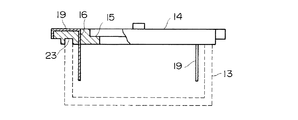
図1において、11は金属化フィルムコンデンサ素子を示し、12、12はメタリコン金属溶射によって素子11の両巻回端に形成した電極引出部である。13は素子11を収容している樹脂製ケースで、その上面の開口には蓋状の樹脂製端子板14が被着されている。端子板14は、上方が漏斗状に拡がった窓15と、両端縁14a、14aと窓15との間にあって両端縁に平行しているスリット状の端子孔16、16とが穿設され、かつ上面の適所に小突起17、17が穿設され、下面の端子孔16、16と両端縁14a、14aとに挟まれた部分からは端子板14と一体に形成された舌片18、18が垂下している。
【0012】
19、19は端子金具で、図1(d)に示すような羽子板形の金属板を折曲して形成され、端子板の両端縁14a、14aと端子孔16、16との間において端子板14の上面と略同一平面内に置かれる端子部19a、19aと、端子部から折曲されて端子孔16、16内に圧入されてケース13内へ垂下する素子接続部19b、19bと、端子板の両端縁14a、14aに沿って折曲された端縁部19c、19cとからなる。
【0013】
素子11は、端子金具の接続部19b、19bの間に半田付けまたは溶接によって接続された上でケース13に収容され、窓15からケース13内に樹脂質充填物20が充填され、その硬化によりコンデンサが完成する。舌片18は素子11をケース13に収容して充填物20を注入した際に、ケース13の内壁との間の摩擦によって素子11が浮力によって浮上するのを防いでいる。舌片18のケース内壁との接触面に突起18aを設けるときは、舌片18とケース内壁との接触が確実になり、更に突起18aに対応してケース内壁側にこれと係合する突起を設けるときは、更に確実に端子板14をケース13に結合することができる。
【0014】
プリント基板への装着は、上記コンデンサを上下転倒させた状態にして基板の結合孔に小突起17、17を挿通し、端子金具19、19の端子部19a、19aを基板導体上に置いて半田付けを実施する。このとき、半田付けが良好に行なわれている場合は、半田が基板導体面から端子金具19、19の端縁部19c、19cに沿って立上がるので、容易にこれを確認することができ、更に基板との機械的結合は小突起17、17の基板結合孔への嵌合によって高められる。
【0015】
【実施例2】
図2は端子板14の図1とは異なる実施例を示し、図1における舌片18、18に代えて、全周がケース13の内壁に接触する囲壁21が存し、囲壁21にはケース内壁に接触する突条21aが全周に設けられている。本実施例では、端子板14とケース13の結合をより確実にできるほか、ケース内への充填物の注入時に端子板14とケース13の隙間から充填物が漏洩するのを防ぐことができる。
【0016】
【実施例3】
図3も端子板14の図1とは異なる実施例を示し、囲壁22がケース13の開口縁の外面を包囲するように設けられている。囲壁22の内周面には全周に突条22aを設けることが望ましい。本実施例の作用、効果は実施例2と同様である。
【0017】
【実施例4】
図4に示す実施例では、図2及び図3に示した囲壁21、22に代えて、端子板14の下面にはケース13の開口縁が嵌入する溝23が設けられており、同様に端子板14とケース13の結合を確実にするほか、充填物20の注入時における漏洩を防いでいる。なお、本実施例では端子板14の窓15は、漏斗状ではなく。階段状に上方が拡大されている。
【0018】
【発明の効果】
以上の実施例から明らかなように、本発明によるときは取付面に広い面積の金属端子を有する面実装型電子部品を実現することができ、その製作に当たって絶縁性充填物に亀裂を生ずることがないために湿気等の侵入がなく、従って信頼性並びに機械的強度が高い電子回路を得ることができる。
【図面の簡単な説明】
【図1】本発明の第1実施例を示し、(a)は断面図、(b)は平面図、(c)は端子板の正面図、(d)は端子金具を展開した平面図である。
【図2】本発明の第2実施例における端子板の一部切断正面図である。
【図3】本発明の第3実施例における端子板の一部切断正面図である。
【図4】本発明の第4実施例における端子板の一部切断正面図である。
【図5】従来の金属化フィルムコンデンサの一例を示し、(a)は平面図、(b)は(a)図におけるA−A線に沿う断面図、(c)は(a)図におけるB−B線に沿う断面図である。
【符号の説明】
11 金属化フィルムコンデンサ素子
12 電極引出部
13 ケース
14 端子板
15 窓
16 端子孔
17 突起
18 舌片
19 端子金具
19a 端子部
19b 素子接続部
19c 端縁部
20 充填物
21 囲壁
22 囲壁
23 溝[0001]
BACKGROUND OF THE INVENTION
The present invention relates to an electronic component suitable for surface mounting on a printed circuit board or the like, and more particularly to a leadless type relatively large capacity capacitor.
[0002]
[Prior art]
Conventionally, for example, as a resin-coated metallized film capacitor, there is a type as shown in FIG. That is, this capacitor is wound by overlapping a pair of metallized films, and provided with
[0003]
[Problems to be solved by the invention]
Generally, when attaching an electronic component having a lead wire to a printed circuit board, it is common to insert the lead wire through a through hole provided in the substrate and then solder this to the board conductor. As work has been automated, metalized film capacitors have been required to be surface-mountable.
[0004]
In the metallized film capacitor having the above-described lead line, the
[0005]
[Means for Solving the Problems]
An electronic component according to the present invention includes a resin case having an open upper surface, a plate-shaped resin terminal plate attached to the upper surface of the case, and terminal fittings supported on both ends of the terminal plate. And an electronic component element housed in the case, and an insulating filler filled in the case. The terminal board has a window at its substantially central portion, and the insulating filler is filled in the case up to the height of the window. Further, the terminal fitting penetrates through a plate-like terminal portion whose upper surface is located in substantially the same plane as the upper surface of the terminal plate, and slit-like terminal holes provided on both ends of the terminal plate. And an element connecting portion hanging down into the case, and the element connecting portion is connected to the electronic component element in the case.
[0006]
[Action]
Unlike the conventional electronic parts with lead lines, the above electronic parts do not need to bend the lead lines for surface mounting, and therefore do not cause cracks in the insulating filler. There is no degradation of the mechanical characteristics. Further, since the terminal fitting is soldered to a conductor such as a printed board over a wide area unlike the lead wire, the reliability of soldering and the mounting strength to the board are remarkably improved.
[0007]
DETAILED DESCRIPTION OF THE INVENTION
It is desirable that the terminal plate is provided with a low surrounding wall that fits on the outer periphery or inner periphery of the opening edge of the case or a groove that fits on the opening edge of the case. It is possible to prevent the conductive filler from overflowing from the joint gap between the terminal plate and the case when it is filled and to contaminate the outer surface of the case, and to prevent the terminal plate and the electronic component element from floating due to buoyancy. In addition, it is desirable that the surrounding wall be provided with a ridge that contacts the case over the entire circumference, thereby more effectively preventing the insulating filler from overflowing from the gap between the case and the terminal plate. Can be prevented. Furthermore, it is desirable to provide a groove on the case side for fitting the ridge on the surrounding wall side, or to provide a ridge above and adjacent to the contact point of the ridge. Engagement with the groove or ridge on the side makes it possible to make the connection between the case and the terminal plate more reliable, and to reduce the overflow of the insulating filler from the gap.
[0008]
In addition, when the terminal plate has no groove or surrounding wall as described above, the terminal plate is integrally formed with a tongue piece that hangs into the case from an appropriate position on the peripheral edge thereof, and contacts the inner surface of the case. If necessary, it is desirable to provide a protrusion at the contact portion of the tongue piece with the inner surface of the case, thereby suppressing the floating of the terminal plate and the electronic component element when the insulating filler is injected. Further, on the case side, a protrusion is provided above and adjacent to the recess into which the protrusion is fitted or the contact position of the protrusion, and if the protrusion on the tongue piece side is engaged with this, the case and the terminal plate Bonding is more secure.
[0009]
The edge of the window of the terminal board is preferably widened in a funnel shape or a stepped shape so that the top surface of the terminal board has a height in the window and does not overflow upward from the window when the insulative filler is injected. It becomes easy to regulate the injection amount. In addition, on the upper surface of the terminal board, a protrusion that engages with a mounting hole formed in a printed circuit board or the like may be provided at an appropriate position as necessary. It is possible to prevent the electronic component from moving and to further increase the mounting strength of the electronic component on the substrate or the like.
[0010]
In addition, it is desirable that the terminal fitting has an end edge portion bent along the end edge of the terminal plate connected to the terminal portion. That is, if the soldering between the terminal portion and the board conductor is performed well, the solder flows to the edge portion, so that it is possible to visually determine whether the soldering is good or bad.
[0011]
[Example 1]
In FIG. 1, 11 indicates a metallized film capacitor element, and 12 and 12 are electrode lead portions formed at both winding ends of the element 11 by metallicon metal spraying.
[0012]
[0013]
The element 11 is accommodated in the
[0014]
For mounting on the printed circuit board, the capacitor is turned upside down, the
[0015]
[Example 2]
FIG. 2 shows an embodiment different from FIG. 1 of the
[0016]
[Example 3]
FIG. 3 also shows an embodiment different from FIG. 1 of the
[0017]
[Example 4]
In the embodiment shown in FIG. 4, in place of the surrounding
[0018]
【The invention's effect】
As is clear from the above embodiments, according to the present invention, it is possible to realize a surface mount type electronic component having a metal terminal with a large area on the mounting surface, and the insulating filler may be cracked during its manufacture. Therefore, it is possible to obtain an electronic circuit that does not intrude moisture or the like and therefore has high reliability and high mechanical strength.
[Brief description of the drawings]
1A and 1B show a first embodiment of the present invention, in which FIG. 1A is a cross-sectional view, FIG. 1B is a plan view, FIG. 1C is a front view of a terminal plate, and FIG. is there.
FIG. 2 is a partially cut front view of a terminal board according to a second embodiment of the present invention.
FIG. 3 is a partially cut front view of a terminal board according to a third embodiment of the present invention.
FIG. 4 is a partially cut front view of a terminal board according to a fourth embodiment of the present invention.
5A and 5B show an example of a conventional metalized film capacitor, wherein FIG. 5A is a plan view, FIG. 5B is a cross-sectional view taken along line AA in FIG. 5A, and FIG. 5C is B in FIG. It is sectional drawing which follows the -B line.
[Explanation of symbols]
DESCRIPTION OF SYMBOLS 11 Metallized film capacitor |
Claims (9)
Priority Applications (1)
| Application Number | Priority Date | Filing Date | Title |
|---|---|---|---|
| JP12638999A JP4339955B2 (en) | 1999-05-06 | 1999-05-06 | Electronic components |
Applications Claiming Priority (1)
| Application Number | Priority Date | Filing Date | Title |
|---|---|---|---|
| JP12638999A JP4339955B2 (en) | 1999-05-06 | 1999-05-06 | Electronic components |
Publications (2)
| Publication Number | Publication Date |
|---|---|
| JP2000323355A JP2000323355A (en) | 2000-11-24 |
| JP4339955B2 true JP4339955B2 (en) | 2009-10-07 |
Family
ID=14933939
Family Applications (1)
| Application Number | Title | Priority Date | Filing Date |
|---|---|---|---|
| JP12638999A Expired - Lifetime JP4339955B2 (en) | 1999-05-06 | 1999-05-06 | Electronic components |
Country Status (1)
| Country | Link |
|---|---|
| JP (1) | JP4339955B2 (en) |
Families Citing this family (7)
| Publication number | Priority date | Publication date | Assignee | Title |
|---|---|---|---|---|
| JP5233294B2 (en) * | 2008-01-28 | 2013-07-10 | パナソニック株式会社 | Electronic components |
| JP2011018813A (en) * | 2009-07-10 | 2011-01-27 | Nippon Chemicon Corp | Plastic molding capacitor |
| JP4868038B2 (en) * | 2009-08-18 | 2012-02-01 | Tdk株式会社 | Electronic components |
| KR101158384B1 (en) | 2010-01-22 | 2012-06-22 | 주식회사 뉴인텍 | Case moldig type capacitor assembly |
| CN110998767B (en) * | 2017-08-02 | 2022-01-04 | 松下知识产权经营株式会社 | Capacitor with a capacitor element |
| JP7024796B2 (en) * | 2017-10-30 | 2022-02-24 | 昭和電工マテリアルズ株式会社 | Film capacitor manufacturing method, case and film capacitor |
| CN115605971A (en) * | 2020-07-07 | 2023-01-13 | 松下知识产权经营株式会社(Jp) | Capacitor with a capacitor element |
-
1999
- 1999-05-06 JP JP12638999A patent/JP4339955B2/en not_active Expired - Lifetime
Also Published As
| Publication number | Publication date |
|---|---|
| JP2000323355A (en) | 2000-11-24 |
Similar Documents
| Publication | Publication Date | Title |
|---|---|---|
| US6922130B2 (en) | Surface mount coil with edgewise winding | |
| US7911042B2 (en) | Package having shield case | |
| KR101934577B1 (en) | Electric connecting terminal for reflowing soldering | |
| US8053685B2 (en) | Metal wiring plate | |
| US6338634B1 (en) | Surface mount electrical connector with anti-wicking terminals | |
| JP4339955B2 (en) | Electronic components | |
| EP1727407A3 (en) | Wired circuit board | |
| KR102340421B1 (en) | Electric conductive gasket with assembly strength improved | |
| JP2000323352A (en) | Electronic parts | |
| JP4339956B2 (en) | Electronic components | |
| JP4396734B2 (en) | Surface mount electronic components | |
| US5107324A (en) | Two-terminal semiconductor device of surface installation type | |
| JP3080880B2 (en) | Chip type solid electrolytic capacitor | |
| KR102594639B1 (en) | Clip gasket preventing stress concentration | |
| US5830014A (en) | Electrical connector | |
| JP4218912B2 (en) | Electronic components | |
| JP3601585B2 (en) | Chip type aluminum electrolytic capacitor | |
| JP2003197828A (en) | Resin-sealing semiconductor device | |
| CN213401213U (en) | SMD diode with dampproofing structure | |
| JPH0529122U (en) | Chip type electronic parts | |
| US20180070449A1 (en) | Electronic device | |
| JPH0234463B2 (en) | ||
| JPH0735342Y2 (en) | Printed circuit board socket | |
| US20210305723A1 (en) | Joint structure for connection of flat electric wire assembly | |
| JP3723863B2 (en) | Reactor manufacturing method |
Legal Events
| Date | Code | Title | Description |
|---|---|---|---|
| A621 | Written request for application examination |
Free format text: JAPANESE INTERMEDIATE CODE: A621 Effective date: 20051114 |
|
| A977 | Report on retrieval |
Free format text: JAPANESE INTERMEDIATE CODE: A971007 Effective date: 20080731 |
|
| A131 | Notification of reasons for refusal |
Free format text: JAPANESE INTERMEDIATE CODE: A131 Effective date: 20080819 |
|
| A521 | Written amendment |
Free format text: JAPANESE INTERMEDIATE CODE: A523 Effective date: 20081020 |
|
| TRDD | Decision of grant or rejection written | ||
| A01 | Written decision to grant a patent or to grant a registration (utility model) |
Free format text: JAPANESE INTERMEDIATE CODE: A01 Effective date: 20090630 |
|
| A01 | Written decision to grant a patent or to grant a registration (utility model) |
Free format text: JAPANESE INTERMEDIATE CODE: A01 |
|
| A61 | First payment of annual fees (during grant procedure) |
Free format text: JAPANESE INTERMEDIATE CODE: A61 Effective date: 20090703 |
|
| R150 | Certificate of patent or registration of utility model |
Free format text: JAPANESE INTERMEDIATE CODE: R150 |
|
| FPAY | Renewal fee payment (event date is renewal date of database) |
Free format text: PAYMENT UNTIL: 20120710 Year of fee payment: 3 |
|
| FPAY | Renewal fee payment (event date is renewal date of database) |
Free format text: PAYMENT UNTIL: 20120710 Year of fee payment: 3 |
|
| FPAY | Renewal fee payment (event date is renewal date of database) |
Free format text: PAYMENT UNTIL: 20130710 Year of fee payment: 4 |
|
| R250 | Receipt of annual fees |
Free format text: JAPANESE INTERMEDIATE CODE: R250 |
|
| R250 | Receipt of annual fees |
Free format text: JAPANESE INTERMEDIATE CODE: R250 |
|
| R250 | Receipt of annual fees |
Free format text: JAPANESE INTERMEDIATE CODE: R250 |
|
| R250 | Receipt of annual fees |
Free format text: JAPANESE INTERMEDIATE CODE: R250 |
|
| R250 | Receipt of annual fees |
Free format text: JAPANESE INTERMEDIATE CODE: R250 |
|
| R250 | Receipt of annual fees |
Free format text: JAPANESE INTERMEDIATE CODE: R250 |
|
| EXPY | Cancellation because of completion of term |