JP4335234B2 - Analog / digital conversion circuit - Google Patents
Analog / digital conversion circuit Download PDFInfo
- Publication number
- JP4335234B2 JP4335234B2 JP2006174563A JP2006174563A JP4335234B2 JP 4335234 B2 JP4335234 B2 JP 4335234B2 JP 2006174563 A JP2006174563 A JP 2006174563A JP 2006174563 A JP2006174563 A JP 2006174563A JP 4335234 B2 JP4335234 B2 JP 4335234B2
- Authority
- JP
- Japan
- Prior art keywords
- output
- input
- side output
- output element
- analog
- Prior art date
- Legal status (The legal status is an assumption and is not a legal conclusion. Google has not performed a legal analysis and makes no representation as to the accuracy of the status listed.)
- Expired - Fee Related
Links
Images


Landscapes
- Analogue/Digital Conversion (AREA)
- Electronic Switches (AREA)
- Amplifiers (AREA)
Description
本発明は、完全な0レベルの入力信号に対してアナログ/デジタル変換回路のループ特性に応じて発生するノイズが可聴帯域の出力信号に与える影響を回避することが可能なアナログ/デジタル変換回路に関する。 The present invention relates to an analog / digital conversion circuit capable of avoiding the influence of noise generated according to the loop characteristics of an analog / digital conversion circuit on an input signal of a complete zero level on an output signal in an audible band. .
音響機器等に搭載される、アナログ信号をデジタル信号に変換するアナログ/デジタル変換回路については、完全な0レベルの入力信号に対してアナログ/デジタル変換回路のループ特性に応じて発生するノイズ(以下、単にこのようなノイズを「巡回ノイズ」と称す)が可聴帯域の出力信号に与える影響が問題とされている。 For analog / digital conversion circuits that convert analog signals to digital signals, which are mounted on audio equipment, etc., noise generated according to the loop characteristics of the analog / digital conversion circuit (hereinafter referred to as the analog / digital conversion circuit) However, the influence of such noise on the output signal in the audible band is a problem.
上記の巡回ノイズの対策として、以下に説明するような2通りの方法が従来講じられていた。 As countermeasures against the above-described cyclic noise, two methods as described below have been conventionally taken.
その1つの方法は、アナログ/デジタル変換回路の帯域外の信号をディザとして混入する方法である。たとえば、帯域が20KHzのアナログ/デジタル変換回路に対して、100KHz程度の大きな周波数の信号をディザとして混入する。これにより、入力信号が完全な「0」レベルであるときにも、入力信号が100KHzである場合と同様となる。したがって、巡回ノイズ成分を可聴帯域外に押しやることができる。 One method is to mix signals outside the band of the analog / digital conversion circuit as dither. For example, a signal having a large frequency of about 100 KHz is mixed as a dither for an analog / digital conversion circuit having a band of 20 KHz. Thus, even when the input signal is at a complete “0” level, it is the same as when the input signal is 100 KHz. Therefore, the cyclic noise component can be pushed out of the audible band.
もう1つの方法は、DCオフセットを入力信号に加算する方法である。たとえば、帯域が20KHzのアナログ/デジタル変換回路に対して、100KHz程度まで入力信号にDCオフセットを加算する。これにより、入力信号が完全な「0」レベルであるときにも、入力信号が100KHzである場合と同様となる。したがって、巡回ノイズ成分を可聴帯域外に押しやることができる。 Another method is to add a DC offset to the input signal. For example, a DC offset is added to the input signal up to about 100 KHz for an analog / digital conversion circuit with a band of 20 KHz. Thus, even when the input signal is at a complete “0” level, it is the same as when the input signal is 100 KHz. Therefore, the cyclic noise component can be pushed out of the audible band.
しかしながら、上記したディザを混入する方法では、ディザを生成するとともに、アナログ/デジタル変換回路の出力段において、ディザを除去する必要がある。そのようなディザの生成および除去のための回路をアナログ/デジタル変換回路に備えている必要があり、アナログ/デジタル変換回路の回路設計が複雑になるという問題点が生ずる。 However, in the above-described method of mixing dither, it is necessary to generate dither and to remove dither at the output stage of the analog / digital conversion circuit. A circuit for generating and removing such a dither needs to be provided in the analog / digital conversion circuit, which causes a problem that the circuit design of the analog / digital conversion circuit becomes complicated.
一方、DCオフセットを入力信号に加算する方法においては、アナログ/デジタル変換回路の出力段におけるDCオフセットの影響を無くすため、ハイパスフィルターをアナログ/デジタル変換回路の出力段に備えている必要がある。したがって、上記したディザを混入する方法と同様に、アナログ/デジタル変換回路の回路設計が複雑になるという問題が生じる。 On the other hand, in the method of adding the DC offset to the input signal, it is necessary to provide a high-pass filter in the output stage of the analog / digital conversion circuit in order to eliminate the influence of the DC offset in the output stage of the analog / digital conversion circuit. Therefore, similarly to the above-described method of mixing dither, there arises a problem that the circuit design of the analog / digital conversion circuit becomes complicated.
本発明は、上記従来の問題点に鑑みなされたものであって、その目的は、簡易な回路設計にて、巡回ノイズが可聴帯域の出力信号に与える影響を低減することが可能なアナログ/デジタル変換回路を提供することにある。 The present invention has been made in view of the above-described conventional problems, and an object of the present invention is to provide an analog / digital that can reduce the influence of cyclic noise on an output signal in an audible band with a simple circuit design. It is to provide a conversion circuit.
本発明のアナログ/デジタル変換回路は、上記課題を解決するため、アナログ/デジタル変換されたデジタル信号に基づいて、ハイサイド出力素子と、ロウサイド出力素子とを交互に駆動することにより、上記デジタル信号を増幅出力するスイッチング手段を備え、上記ハイサイド出力素子をオン状態にする時間と、上記ロウサイド出力素子をオン状態にする時間とが異なるように設定することができるバランス調整手段を備えるアナログ/デジタル変換回路であって、上記バランス調整手段を用いて、上記ハイサイド出力素子及び上記ロウサイド出力素子のいずれかに、DCオフセットを与えた状態と同じ状態にすることを特徴としている。 In order to solve the above problems, the analog / digital conversion circuit of the present invention drives the high-side output element and the low-side output element alternately based on the analog / digital-converted digital signal to thereby generate the digital signal. Analog / digital having a balance adjusting means capable of setting the time for turning on the high-side output element to be different from the time for turning on the low-side output element. A conversion circuit, characterized in that the balance adjustment means is used to bring a DC offset into the same state as any of the high-side output element and the low-side output element .
また、本発明のアナログ/デジタル変換回路は、上記構成にくわえて、上記バランス調整手段は、上記ハイサイド出力素子と上記ロウサイド出力素子とを異なる電位で駆動することで、上記ハイサイド出力素子及び上記ロウサイド出力素子のいずれかに、DCオフセットを与えた状態と同じ状態にすることが好ましい。 Further, in the analog / digital conversion circuit of the present invention, in addition to the above-described configuration, the balance adjusting unit drives the high-side output element and the low-side output element at different potentials, so that the high-side output element and the low-side output element It is preferable that one of the low-side output elements is in the same state as a state where a DC offset is applied.
また、本発明のアナログ/デジタル変換回路は、上記構成にくわえて、上記バランス調整手段は、上記ハイサイド出力素子及び上記ロウサイド出力素子のいずれかに、DCオフセットを与えた状態と同じ状態にすることで、完全な0レベルの入力信号に対してアナログ/デジタル変換回路のループ特性に応じて発生する巡回ノイズによって発生するスペクトラムを、可聴帯域外に押しやることが好ましい。Further, in the analog / digital conversion circuit of the present invention, in addition to the above configuration, the balance adjusting means is in the same state as a state where a DC offset is applied to either the high side output element or the low side output element. Thus, it is preferable to push the spectrum generated by the cyclic noise generated according to the loop characteristics of the analog / digital conversion circuit to the input signal of 0 level completely outside the audible band.
すなわち、アナログ/デジタル変換回路は、アナログ/デジタル変換されたデジタル信号に基づいて、ハイサイド出力素子と、ロウサイド出力素子とを、スイッチング手段を用いて交互に駆動することにより、上記デジタル信号を増幅出力する。 That is, the analog / digital conversion circuit amplifies the digital signal by alternately driving the high-side output element and the low-side output element using switching means based on the analog / digital converted digital signal. Output.
ところで、アナログ/デジタル変換回路においては、完全な0レベルの入力信号に対してアナログ/デジタル変換回路のループ特性に応じて発生するノイズ(巡回ノイズ)が可聴帯域の出力信号に与える影響が問題とされている。 By the way, in the analog / digital conversion circuit, there is a problem that the noise (cyclic noise) generated according to the loop characteristics of the analog / digital conversion circuit with respect to a complete zero level input signal has an influence on the output signal in the audible band. Has been.
そこで、本発明では、特に、上記ハイサイド出力素子をオン状態にする時間と、および上記ロウサイド出力素子をオン状態にする時間とが異なるように設定することで、完全な0レベルの入力信号に対してアナログ/デジタル変換回路のループ特性に応じて発生する巡回ノイズによって発生するスペクトラムを、可聴帯域外に押しやる。 Therefore, in the present invention, in particular, by setting the time for turning on the high-side output element to be different from the time for turning on the low-side output element, a completely zero-level input signal can be obtained. On the other hand, the spectrum generated by the cyclic noise generated according to the loop characteristics of the analog / digital conversion circuit is pushed out of the audible band.
上記の構成によれば、ハイサイド出力素子をオン状態にする時間と、ロウサイド出力素子をオン状態とする時間とが異なるように設定することができる。すなわち、ハイサイド出力素子と、ロウサイド出力素子とを、異なる電位にて駆動することができる。したがって、ハイサイド出力素子またはロウサイド出力素子のいずれかに、DCオフセットを与えた状態と同じ状態とすることができる。 According to the above configuration, the time for turning on the high-side output element can be set different from the time for turning on the low-side output element. That is, the high-side output element and the low-side output element can be driven with different potentials. Therefore, the same state as that in which a DC offset is applied to either the high-side output element or the low-side output element can be obtained.
これにより、巡回ノイズによって発生するスペクトラムを、可聴帯域外に押しやることができる。また、ハイサイド出力素子をオン状態にする時間と、上記ロウサイド出力素子をオン状態にする時間とのバランスは、アナログ/デジタル変換回路内部において調整可能であり、アナログ/デジタル変換回路の出力段や入力段に特別な回路を設ける必要が無い。 As a result, the spectrum generated by the cyclic noise can be pushed out of the audible band. The balance between the time for turning on the high-side output element and the time for turning on the low-side output element can be adjusted inside the analog / digital conversion circuit. There is no need to provide a special circuit in the input stage.
それゆえ、簡易な回路設計にて、巡回ノイズが可聴帯域の出力信号に与える影響を低減することが可能なアナログ/デジタル変換回路を提供することができるという効果を奏する。 Therefore, it is possible to provide an analog / digital conversion circuit capable of reducing the influence of cyclic noise on an audible band output signal with a simple circuit design.
また、本発明のアナログ/デジタル変換回路は、上記構成にくわえて、上記バランス調整手段は、プラス側の入力端子および出力端子と、マイナス側の入力端子および出力端子とを備えているとともに、上記プラス側の入力端子と出力端子との間、および上記マイナス側の入力端子と出力端子との間には、抵抗と、上記抵抗と直列に接続されたコンデンサと、上記抵抗にフィードバック接続されたダイオードとを有している回路がそれぞれ接続されている一方、上記プラス側の入力端子と出力端子との間に接続された上記抵抗と上記コンデンサとにより決定される時定数と、上記マイナス側の入力端子と出力端子との間に接続された上記抵抗と上記コンデンサとにより決定される時定数とが異なることが好ましい。 The analog / digital converter circuit of the present invention, in addition to the above structure, the upper Symbol balance adjusting means, an input terminal and an output terminal of the plus side, with and an input terminal and an output terminal on the negative side, Between the positive side input terminal and the output terminal, and between the negative side input terminal and the output terminal, a resistor, a capacitor connected in series with the resistor, and a feedback connection to the resistor are connected. Each circuit having a diode is connected, while the time constant determined by the resistor and the capacitor connected between the positive input terminal and the output terminal, and the negative side It is preferable that a time constant determined by the resistor and the capacitor connected between the input terminal and the output terminal is different .
上記の構成によれば、バランス調整手段は、抵抗とコンデンサとからなる積分回路を構成するとともに、抵抗にはダイオードがフィードバック接続されている。また、バランス調整手段におけるプラス側の入力端子と出力端子との間に接続された抵抗とコンデンサとにより決定される時定数と、バランス調整手段におけるマイナス側の入力端子と出力端子との間に接続された抵抗とコンデンサとにより決定される時定数とが異なる。 According to the above configuration, the balance adjusting unit forms an integrating circuit including a resistor and a capacitor, and a diode is feedback-connected to the resistor. Also, a time constant determined by a resistor and a capacitor connected between the positive input terminal and the output terminal in the balance adjusting means, and a connection between the negative input terminal and the output terminal in the balance adjusting means. The time constant determined by the resistance and the capacitor is different.
したがって、バランス調整手段のプラス側の入力端子にあるクロックパルスを入力すると、プラス側の出力端子には、上記クロックパルスよりも立ち上がりタイミングが時間ΔT1だけ遅れ、上記クロックパルスと立ち下がりタイミングが同じであるクロックパルスが出力される。 Therefore, when a clock pulse at the positive input terminal of the balance adjusting means is input, the rising timing is delayed by a time ΔT1 from the clock pulse at the positive output terminal, and the falling timing is the same as the clock pulse. A clock pulse is output.
また、マイナス側の入力端子には、プラス側の入力端子に入力されたクロックパルスを反転したクロックパルスが入力される。そして、マイナス側の出力端子には、上記の反転されたクロックパルスよりも立ち上がりが時間ΔT2だけ遅れ、反転されたクロックパルスと立ち下がりタイミングが同じであるクロックパルスが出力される。 Further, a clock pulse obtained by inverting the clock pulse input to the positive input terminal is input to the negative input terminal. Then, the negative output terminal outputs a clock pulse whose rising edge is delayed by the time ΔT2 from the inverted clock pulse and whose falling timing is the same as that of the inverted clock pulse.
ここで、プラス側の入力端子と出力端子との間に接続された抵抗とコンデンサとにより決定される時定数と、マイナス側の入力端子と出力端子との間に接続された抵抗とコンデンサとにより決定される時定数とが異なるため、上記のΔT1とΔT2とは、異なる値となる。 Here, the time constant determined by the resistor and the capacitor connected between the positive input terminal and the output terminal, and the resistor and the capacitor connected between the negative input terminal and the output terminal Since the time constant to be determined is different, the above ΔT1 and ΔT2 have different values.
すなわち、バランス調整手段のプラス側の出力端子から出力されるクロックパルスと、マイナス側の出力端子から出力されるクロックパルスとのそれぞれにおいて、電圧がHigh状態となる時間は異なるものとなる。したがって、バランス調整手段のプラス側の出力端子から出力されるクロックパルスと、マイナス側の出力端子から出力されるクロックパルスとを、ハイサイド出力素子およびロウサイド出力素子を駆動するための信号としてスイッチング手段に出力すれば、ハイサイド出力素子をオン状態にする時間と、ロウサイド出力素子をオン状態とする時間とが異なるように設定することができる。 That is, the time during which the voltage is in the high state differs between the clock pulse output from the plus output terminal of the balance adjusting unit and the clock pulse output from the minus output terminal. Therefore, the switching means uses the clock pulse output from the positive output terminal of the balance adjusting means and the clock pulse output from the negative output terminal as signals for driving the high-side output element and the low-side output element. In this case, the time for turning on the high side output element and the time for turning on the low side output element can be set differently.
それゆえ、ハイサイド出力素子またはロウサイド出力素子のいずれかに、DCオフセットを与えた状態と同じ状態とし、巡回ノイズによって発生するスペクトラムを、可聴帯域外に押しやることができる。また、巡回ノイズを回避するための構成を、バランス調整手段に、抵抗と、コンデンサと、ダイオードとにより構成するという簡易な構成により実現することができる。 Therefore, it is possible to set the same state as a state where a DC offset is applied to either the high-side output element or the low-side output element and push the spectrum generated by the cyclic noise out of the audible band. Further, the configuration for avoiding the cyclic noise can be realized by a simple configuration in which the balance adjusting means is configured by a resistor, a capacitor, and a diode.
これにより、より簡易な回路設計にて巡回ノイズが可聴帯域の出力信号に与える影響を低減することが可能なアナログ/デジタル変換回路を提供することができるという効果を奏する。 As a result, it is possible to provide an analog / digital conversion circuit capable of reducing the influence of cyclic noise on an audible band output signal with a simpler circuit design.
また、本発明のアナログ/デジタル変換回路は、上記構成にくわえて、上記バランス調整手段は、プラス側の入力端子および出力端子と、マイナス側の入力端子および出力端子とを備えているとともに、上記プラス側の入力端子に入力されるデジタル信号の立ち上がりを時間ΔT1だけ遅延させる一方、該デジタル信号の立ち下がりを遅延させずに上記プラス側の出力端子に出力するとともに、上記マイナス側の入力端子に入力されるデジタル信号の立ち上がりを上記ΔT1と異なる時間である時間ΔT2だけ遅延させる一方、該デジタル信号の立ち下がりを遅延させずに上記マイナス側の出力端子に出力することが好ましい。 The analog / digital converter circuit of the present invention, in addition to the above structure, the upper Symbol balance adjusting means, an input terminal and an output terminal of the plus side, with and an input terminal and an output terminal on the negative side, While delaying the rising edge of the digital signal input to the positive input terminal by time ΔT1, the digital signal is output to the positive output terminal without delaying the falling edge of the digital signal, and the negative input terminal It is preferable that the rising edge of the digital signal input to is delayed by a time ΔT2, which is a time different from ΔT1, while the falling edge of the digital signal is output to the negative output terminal without delaying .
上記の構成によれば、バランス調整手段のプラス側の入力端子にあるクロックパルスを入力し、そのクロックパルスを反転したクロックパルスをマイナス側の入力端子に入力することにより、バランス調整手段のプラス側の出力端子から出力されるクロックパルスと、マイナス側の出力端子から出力されるクロックパル
スとのそれぞれにおいて、電圧がHigh状態となる時間は異なるものとなる。
According to the above configuration, the clock pulse at the positive input terminal of the balance adjustment unit is input, and the clock pulse obtained by inverting the clock pulse is input to the negative input terminal. The clock pulse output from the output terminal and the clock pulse output from the negative output terminal have different times during which the voltage is in the high state.
したがって、バランス調整手段のプラス側の出力端子から出力されるクロックパルスと、マイナス側の出力端子から出力されるクロックパルスとを、ハイサイド出力素子およびロウサイド出力素子を駆動するための信号としてスイッチング手段に出力すれば、ハイサイド出力素子をオン状態にする時間と、ロウサイド出力素子をオン状態とする時間とが異なるように設定することができる。 Therefore, the switching means uses the clock pulse output from the positive output terminal of the balance adjusting means and the clock pulse output from the negative output terminal as signals for driving the high-side output element and the low-side output element. In this case, the time for turning on the high side output element and the time for turning on the low side output element can be set differently.
それゆえ、ハイサイド出力素子またはロウサイド出力素子のいずれかに、DCオフセットを与えた状態と同じ状態とし、巡回ノイズによって発生するスペクトラムを、可聴帯域外に押しやることができる。 Therefore, it is possible to set the same state as a state where a DC offset is applied to either the high-side output element or the low-side output element and push the spectrum generated by the cyclic noise out of the audible band.
それゆえ、簡易な回路設計にて、巡回ノイズが可聴帯域の出力信号に与える影響を低減することが可能なアナログ/デジタル変換回路を提供することができるという効果を奏する。 Therefore, it is possible to provide an analog / digital conversion circuit capable of reducing the influence of cyclic noise on an audible band output signal with a simple circuit design.
本発明のアナログ/デジタル変換回路は、以上のように、アナログ/デジタル変換されたデジタル信号に基づいて、ハイサイド出力素子と、ロウサイド出力素子とを交互に駆動することにより、上記デジタル信号を増幅出力するスイッチング手段を備え、上記ハイサイド出力素子をオン状態にする時間と、上記ロウサイド出力素子をオン状態にする時間とが異なるように設定することができるバランス調整手段を備えるアナログ/デジタル変換回路であって、上記バランス調整手段を用いて、上記ハイサイド出力素子及び上記ロウサイド出力素子のいずれかに、DCオフセットを与えた状態と同じ状態にするものである。 As described above, the analog / digital conversion circuit of the present invention amplifies the digital signal by alternately driving the high-side output element and the low-side output element based on the analog / digital converted digital signal. An analog / digital conversion circuit comprising switching means for outputting , and comprising balance adjusting means capable of setting the time for turning on the high-side output element to be different from the time for turning on the low-side output element In this case, the balance adjusting means is used to bring the DC offset into the same state as any of the high-side output element and the low-side output element .
上記の構成によれば、ハイサイド出力素子またはロウサイド出力素子のいずれかに、DCオフセットを与えた状態と同じ状態とすることができる。これにより、巡回ノイズによって発生するスペクトラムを、可聴帯域外に押しやることができる。 According to said structure, it can be set as the same state as the state which gave DC offset to either the high side output element or the low side output element. As a result, the spectrum generated by the cyclic noise can be pushed out of the audible band.
また、ハイサイド出力素子をオン状態にする時間と、ロウサイド出力素子をオン状態にする時間とのバランスは、アナログ/デジタル変換回路内部において調整可能であり、アナログ/デジタル変換回路の出力段や入力段に特別な回路を設ける必要が無い。 Also, the balance between the time for turning on the high-side output element and the time for turning on the low-side output element can be adjusted inside the analog / digital conversion circuit, and the output stage and input of the analog / digital conversion circuit can be adjusted. There is no need to provide a special circuit in the stage.
それゆえ、簡易な回路設計にて、巡回ノイズが可聴帯域の出力信号に与える影響を低減することが可能なアナログ/デジタル変換回路を提供することができるという効果を奏する。 Therefore, it is possible to provide an analog / digital conversion circuit capable of reducing the influence of cyclic noise on an audible band output signal with a simple circuit design.
本発明の実施の一形態について図1ないし図3に基づいて説明すれば、以下の通りである。 One embodiment of the present invention will be described with reference to FIGS. 1 to 3 as follows.
本実施の形態のアナログ/デジタル変換回路1は、図2に示すように、アナログ/デジタルコンバータ(以下、単にADコンバータとする)2と、デッドタイムコントロール回路(バランス調整手段)3と、レベルシフト回路4と、第1ゲートドライバ回路(スイッチング手段、一方側スイッチング手段)5と、第2ゲートドライバ回路(スイッチング手段、他方側スイッチング手段)6と、複数の出力FET(電界効果トランジスタ:Field Effect Transistor )7…とを備えている。
As shown in FIG. 2, the analog /
ADコンバータ2は、外部から差動入力されたアナログ信号を、PDM(Pulse Duration Modulation :パルス期間変調)デジタル信号に変調する。デッドタイムコントロール回路3は、ADコンバータ2から入力されたPDMデジタル信号のパルスの立ち上がりタイミングと立ち下がりタイミングとを調整して、レベルシフト回路4に出力するものである。デッドタイムコントロール回路3の詳細な構成については、後述する。
The AD converter 2 modulates an analog signal differentially input from the outside into a PDM (Pulse Duration Modulation) digital signal. The dead
レベルシフト回路4は、デッドタイムコントロール回路3からの出力信号をレベルシフトするものである。さらに、レベルシフト回路4からのプラス出力は、後述する第1ゲートドライバ回路5のHigh側と、後述する第2ゲートドライバ回路6のLow側に入力されている。一方、レベルシフト回路4からのマイナス出力は、第1ゲートドライバ回路5のLow側と、第2ゲートドライバ回路6のHigh側とに入力されている。
The level shift circuit 4 shifts the level of the output signal from the dead
第1ゲートドライバ回路5は、High側の出力およびLow側の出力のそれぞれに接続された出力FET(一方側ハイサイド出力素子、一方側ロウサイド出力素子)7…を駆動するものである。同様に、第2ゲートドライバ回路6は、High側の出力およびLow側の出力のそれぞれに接続された出力FET(他方側ハイサイド出力素子、他方側ロウサイド出力素子)7…を駆動するものである。 The first gate driver circuit 5 drives output FETs (one-side high-side output element, one-side low-side output element) 7... Connected to the high-side output and the low-side output, respectively. Similarly, the second gate driver circuit 6 drives output FETs (the other side high side output element, the other side low side output element) 7... Connected to the high side output and the low side output, respectively. .
上記の構成により、アナログ/デジタル変換回路1は、ADコンバータ2に入力されたアナログ信号を、第1ゲートドライバ回路5に接続された出力FET7…と、第2ゲートドライバ回路6に接続された出力FET7…とからデジタル信号としてそれぞれ出力する。出力FET7…からのデジタル信号は、ローパスフィルタ8により高周波成分が除去され、外部の負荷9に出力される。
With the above configuration, the analog /
次に、本発明の特徴点であるデッドタイムコントロール回路3の詳細な構成について説明する。
Next, a detailed configuration of the dead
図1に示すように、デッドタイムコントロール回路3におけるプラス側入力とプラス側出力との間には、抵抗R1と、ダイオードD1と、コンデンサC1と、アンドゲートU1とが接続されている。同様に、デッドタイムコントロール回路3におけるマイナス側入力とマイナス側出力との間には、抵抗R2と、ダイオードD2と、コンデンサC2と、アンドゲートU2とが接続されている。
As shown in FIG. 1, a resistor R1, a diode D1, a capacitor C1, and an AND gate U1 are connected between a plus side input and a plus side output in the dead
なお、デッドタイムコントロール回路3におけるプラス側入力とプラス側出力との間の回路構成と、マイナス側入力とマイナス側出力との間の回路構成とは同じであるので、以下の説明では、プラス側入力とプラス側出力との間の回路構成について代表して説明する。
Note that the circuit configuration between the plus side input and the plus side output in the dead
デッドタイムコントロール回路3におけるプラス側入力とプラス側出力との間において、ダイオードD1は、抵抗R1に対してフィードバック接続されている。また、コンデンサC1の一方の接点は、抵抗R1の出力とアンドゲートU1との間に接続されている。一方、コンデンサC1の他方の接点は接地されている。
Between the positive side input and the positive side output in the dead
上記の構成により、コンデンサC1は、ADコンバータ2からデッドタイムコントロール回路3のプラス側に入力されるデジタル信号に対して、時定数R1C1により決定される応答特性により充電される。一方、コンデンサC1が放電される場合には、放電電流はダイオードD1を経由するので、瞬時に放電が行われることとなる。
With the above configuration, the capacitor C1 is charged with a response characteristic determined by the time constant R1C1 with respect to the digital signal input from the AD converter 2 to the plus side of the dead
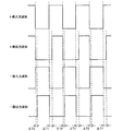
すなわち、図3に示すように、デッドタイムコントロール回路3における、プラス側の入力波形と、プラス側出力波形とを比較した場合、出力波形の立ち上がりが入力波形の立ち上がりに対して一定時間遅れることとなる。一方、コンデンサC1の放電は瞬時に行われるため、プラス側の入力波形と出力波形とを比較した場合に、立ち下がりは同一のタイミングとなる。
That is, as shown in FIG. 3, when comparing the plus-side input waveform and the plus-side output waveform in the dead
上記の入出力波形における立ち上がりの時間のずれをデッドタイムと称し、同図中ΔT1として示している。このデッドタイムΔT1は、デッドタイムコントロール回路3におけるプラス側の入出力を接続する回路の時定数R1C1により決定されるものである。
The rise time lag in the input / output waveform is referred to as dead time, and is shown as ΔT1 in FIG. This dead time ΔT1 is determined by the time constant R1C1 of the circuit connecting the positive input / output in the dead
同様に、マイナス側の入力波形と出力波形とを比較した場合、出力波形の立ち上がりは入力波形に対してデッドタイムΔT2だけ遅れ、出力波形の立ち下がりは入力波形の立ち下がりと同一タイミングとなる。上記のデッドタイムΔT2は、デッドタイムコントロール回路3におけるマイナス側の入出力を接続する回路の時定数R2C2とにより決定されるものである。
Similarly, when the input waveform on the negative side is compared with the output waveform, the rise of the output waveform is delayed by the dead time ΔT2 with respect to the input waveform, and the fall of the output waveform has the same timing as the fall of the input waveform. The dead time ΔT2 is determined by the time constant R2C2 of the circuit connecting the negative input / output in the dead
上記のデッドタイムΔT1の期間は、デッドタイムコントロール回路3のプラス側の出力、およびマイナス側の出力はともにLowレベルである。同様に、デッドタイムΔT2の期間も、プラス側、マイナス側の出力は共にLowレベルとなる。すなわち、デッドタイムΔT1・ΔT2の間は、第1および第2ゲートドライバ回路5・6のHigh側の出力FET7…と、Low側の出力FET7…とは、共にオフ状態となる。
During the period of the dead time ΔT1, both the plus side output and the minus side output of the dead
なお、上記のようにデッドタイムΔT1・T2を設けていない場合、デッドタイムコントロール回路3への入力波形と出力波形との立ち上がりおよび立ち下がりタイミングが同一となり、出力FET7…の立ち上がりおよび立ち下がりの遅れにより、High側の出力FET7と、Low側の出力FET7とを同時にオンするタイミングが発生する。このように、High側の出力FET7と、Low側の出力FET7とを同時にオンすると、回路素子の破壊を誘引し好ましくない。
When the dead times ΔT1 and T2 are not provided as described above, the rising and falling timings of the input waveform and the output waveform to the dead
また、ΔT1と、ΔT2とは、巡回ノイズを回避するため、異なる値に設定されている。より具体的には、ΔT1を決定する時定数R1C1と、ΔT2を決定する時定数R2C2とが異なる値に設定されている。以下、時定数R1C1とR2C2とが異なる値に設定されている理由について説明する。 Further, ΔT1 and ΔT2 are set to different values in order to avoid cyclic noise. More specifically, the time constant R1C1 for determining ΔT1 and the time constant R2C2 for determining ΔT2 are set to different values. Hereinafter, the reason why the time constants R1C1 and R2C2 are set to different values will be described.
ΔT1と、ΔT2とが同じ値である場合は、時定数R1C1と時定数R2C2とは同じ値である。この場合、デッドタイムコントロール回路3へのプラス側に入力された電圧は、抵抗R1とコンデンサC1とにより積分された後、入力電圧の1/2である電位にて出力される。同様に、デッドタイムコントロール回路3のマイナス側に入力された電圧も、抵抗R2とコンデンサC2とにより積分された後、入力電圧の1/2である電位にて出力される。なお、上記のように、入力電圧の1/2である電位にて出力されるのは、出力電圧が入力電圧の平均値となるからである。
When ΔT1 and ΔT2 are the same value, the time constant R1C1 and the time constant R2C2 are the same value. In this case, the voltage input on the plus side to the dead
すなわち、デッドタイムコントロール回路3からのプラス側出力およびマイナス側出力は、後段のレベルシフト回路4(図2)、第1ゲートドライバ回路5(図2)、および第2ゲートドライバ回路6(図2)とを経由して、High側の出力FET7…と、Low側の出力FET7…とを、同じ電位にて駆動する。
That is, the plus side output and the minus side output from the dead
このような場合、巡回ノイズは、High側の出力FET7…と、Low側の出力FET7…とから同じ電位で出力されてしまうので、出力信号に与える影響が大きくなる。 In such a case, the cyclic noise is output at the same potential from the High-side output FETs 7... And the Low-side output FETs 7.
しかしながら、ΔT1とΔT2とが異なる値である場合、デッドタイムコントロール回路3のプラス側出力と、マイナス側出力とは、異なる電位となる。したがって、デッドタイムコントロール回路3からのプラス側出力およびマイナス側出力は、後段のレベルシフト回路4(図2)、第1ゲートドライバ回路5(図2)、および第2ゲートドライバ回路6(図2)とを経由して、High側の出力FET7…と、Low側の出力FET7…とを、異なる電位にて駆動することになる。
However, when ΔT1 and ΔT2 are different values, the plus side output and the minus side output of the dead
すなわち、ΔT1とΔT2とが異なる値である場合、High側の出力FET7あるいはLow側の出力FET7のいずれかにDCオフセットを与えた状態と同じ状態となる。したがって、巡回ノイズによって発生するスペクトラムを、可聴帯域外に押しやることができる。 That is, when ΔT1 and ΔT2 are different values, the state is the same as when a DC offset is applied to either the high-side output FET 7 or the low-side output FET 7. Therefore, the spectrum generated by the cyclic noise can be pushed out of the audible band.
このように、本実施の形態のアナログ/デジタル変換回路1は、アナログ/デジタル変換されたデジタル信号に基づいて、High側の出力FET7と、Low側の出力FET7とを交互に駆動することにより、デジタル信号を増幅出力する第1ゲートドライバ回路5あるいは第2ゲートドライバ回路6を備えているアナログ/デジタル変換回路において、High側の出力FET7をオン状態にする時間と、Low側の出力FET7をオン状態にする時間とのバランスを調整するデッドタイムコントロール回路3を備えているものである。
As described above, the analog /
上記の構成によれば、デッドタイムコントロール回路3により、High側の出力FET7をオン状態にする時間と、Low側の出力FET7をオン状態とする時間とが異なるように設定することができる。すなわち、High側の出力FET7と、Low側の出力FET7とを、異なる電位にて駆動することができる。したがって、High側の出力FET7またはLow側の出力FET7のいずれかに、DCオフセットを与えた状態とすることができる。
According to the above configuration, the dead
これにより、巡回ノイズによって発生するスペクトラムを、可聴帯域外に押しやることができる。また、High側の出力FET7をオン状態にする時間と、Low側の出力FET7をオン状態にする時間とのバランスは、アナログ/デジタル変換回路1内部において調整可能であり、アナログ/デジタル変換回路1の出力段や入力段に特別な回路を設ける必要が無い。
As a result, the spectrum generated by the cyclic noise can be pushed out of the audible band. The balance between the time for turning on the High-side output FET 7 and the time for turning on the Low-side output FET 7 can be adjusted inside the analog /
それゆえ、簡易な回路設計にて、巡回ノイズが可聴帯域の出力信号に与える影響を低減することが可能なアナログ/デジタル変換回路1を提供することができるという効果を奏する。
Therefore, it is possible to provide the analog /
また、本実施の形態のアナログ/デジタル変換回路1は、上記構成のアナログ/デジタル変換回路1において、High側の出力FET7とLow側の出力FET7とを交互に駆動する第1ゲートドライバ回路5と、High側の出力FET7とLow側の出力FET7とを交互に駆動する第2ゲートドライバ回路6とを備えているとともに、High側の出力FET7を駆動する信号を入力するための第1ゲートドライバ回路5への入力ラインと、Low側の出力FET7を駆動する信号を入力するための第2ゲートドライバ回路6への入力とが接続されている一方、Low側の出力FET7を駆動する信号を入力するための第1ゲートドライバ回路5への入力ラインと、High側の出力FET7を駆動する信号を入力するための第2ゲートドライバ回路6への入力ラインとが接続されており、デッドタイムコントロール回路3は、第1ゲートドライバ回路5におけるHigh側の出力FET7をオン状態にする時間とLow側の出力FET7をオン状態にする時間とのバランス、および第2ゲートドライバ回路6におけるHigh側の出力FET7をオン状態にする時間とLow側の出力FET7をオン状態とする時間とのバランスを調整するものである。
Further, the analog /
上記の構成によれば、デッドタイムコントロール回路3により、第1ゲートドライバ回路5におけるHigh側の出力FET7をオン状態にする時間と、Low側の出力FET7をオン状態とする時間とが異なるように設定することができる。同様に、第2ゲートドライバ回路6におけるHigh側の出力FET7をオン状態にする時間と、Low側の出力FET7をオン状態とする時間とが異なるように設定することができる。
According to the above configuration, the time for turning on the High-side output FET 7 in the first gate driver circuit 5 by the dead
すなわち、第1ゲートドライバ回路5においてHigh側の出力FET7およびLow側の出力FET7とを、異なる電位にて駆動することができる。したがって、第1ゲートドライバ回路5におけるHigh側の出力FET7またはLow側の出力FET7のいずれかに、DCオフセットを与えた状態とすることができる。同様に、第2ゲートドライバ回路6におけるLow側の出力FET7またはHigh側の出力FET7のいずれかについても、DCオフセットを与えた状態とすることができる。 That is, in the first gate driver circuit 5, the high-side output FET 7 and the low-side output FET 7 can be driven at different potentials. Therefore, a DC offset can be applied to either the high-side output FET 7 or the low-side output FET 7 in the first gate driver circuit 5. Similarly, either the Low-side output FET 7 or the High-side output FET 7 in the second gate driver circuit 6 can be in a state where a DC offset is applied.
これにより、巡回ノイズによって発生するスペクトラムを、可聴帯域外に押しやることができる。また、High側の出力FET7をオン状態にする時間と、Low側の出力FET7をオン状態にする時間とのバランスは、アナログ/デジタル変換回路1内部において調整可能であり、アナログ/デジタル変換回路1の出力段や入力段に特別な回路を設ける必要が無い。
As a result, the spectrum generated by the cyclic noise can be pushed out of the audible band. The balance between the time for turning on the High-side output FET 7 and the time for turning on the Low-side output FET 7 can be adjusted inside the analog /
さらに、第1ゲートドライバ回路5におけるHigh側の出力FET7および第2ゲートドライバ回路6におけるLow側の出力FET7への入力ラインが接続されているとともに、第1ゲートドライバ回路5におけるLow側の出力FET7および第2ゲートドライバ回路6におけるHigh側の出力FET7への入力ラインが接続されている。したがって、4つの出力素子を、2つの入力信号で駆動することができ、回路設計を簡略化することができる。 Further, input lines to the high-side output FET 7 in the first gate driver circuit 5 and the low-side output FET 7 in the second gate driver circuit 6 are connected, and the low-side output FET 7 in the first gate driver circuit 5. The input line to the high-side output FET 7 in the second gate driver circuit 6 is connected. Therefore, the four output elements can be driven by two input signals, and the circuit design can be simplified.
それゆえ、より簡易な回路設計にて巡回ノイズが可聴帯域の出力信号に与える影響を低減することが可能なアナログ/デジタル変換回路1を提供することができるという効果を奏する。
Therefore, it is possible to provide the analog /
また、本実施の形態のアナログ/デジタル変換回路1は、デッドタイムコントロール回路3は、プラス側の入力端子および出力端子と、マイナス側の入力端子および出力端子とを備えているとともに、プラス側の入力端子と出力端子との間、およびマイナス側の入力端子と出力端子との間には、抵抗R1(R2)と、抵抗R1(R2)と直列に接続されたコンデンサC1(C2)と、抵抗R1(R2)にフィードバック接続されたダイオードD1(D2)とを有している回路がそれぞれ接続されている一方、プラス側の入力端子と出力端子との間に接続された抵抗R1とコンデンサC1とにより決定される時定数R1C1と、マイナス側の入力端子と出力端子との間に接続された抵抗R2とコンデンサC2とにより決定される時定数R2C2とが異なるものである。
In addition, in the analog /
上記の構成によれば、デッドタイムコントロール回路3は、抵抗R1(R2)とコンデンサC1(C2)とからなる積分回路を構成するとともに、抵抗R1(R2)にはダイオードD1(D2)がフィードバック接続されている。また、デッドタイムコントロール回路3におけるプラス側の入力端子と出力端子との間に接続された抵抗R1とコンデンサC1とにより決定される時定数R1C1と、デッドタイムコントロール回路3におけるマイナス側の入力端子と出力端子との間に接続された抵抗R2とコンデンサC2とにより決定される時定数R2C2とが異なる。
According to the above configuration, the dead
したがって、デッドタイムコントロール回路3のプラス側の入力端子にあるクロックパルスを入力すると、プラス側の出力端子には、クロックパルスよりも立ち上がりタイミングが時間ΔT1だけ遅れ、上記クロックパルスと立ち下がりタイミングが同じであるクロックパルスが出力される。
Therefore, when the clock pulse at the positive input terminal of the dead
また、マイナス側の入力端子には、プラス側の入力端子に入力されたクロックパルスを反転したクロックパルスが入力される。そして、マイナス側の出力端子には、上記の反転されたクロックパルスよりも立ち上がりが時間ΔT2だけ遅れ、反転されたクロックパルスと立ち下がりタイミングが同じであるクロックパルスが出力される。 Further, a clock pulse obtained by inverting the clock pulse input to the positive input terminal is input to the negative input terminal. Then, the negative output terminal outputs a clock pulse whose rising edge is delayed by the time ΔT2 from the inverted clock pulse and whose falling timing is the same as that of the inverted clock pulse.
ここで、プラス側の入力端子と出力端子との間に接続された抵抗R1とコンデンサC1とにより決定される時定数R1C1と、マイナス側の入力端子と出力端子との間に接続された抵抗R2とコンデンサC2とにより決定される時定数R2C2とが異なるため、上記のΔT1とΔT2とは、異なる値となる。 Here, a time constant R1C1 determined by the resistor R1 and the capacitor C1 connected between the positive input terminal and the output terminal, and a resistor R2 connected between the negative input terminal and the output terminal. Since the time constant R2C2 determined by the capacitor C2 is different, the above ΔT1 and ΔT2 have different values.
すなわち、デッドタイムコントロール回路3のプラス側の出力端子から出力されるクロックパルスと、マイナス側の出力端子から出力されるクロックパルスとのそれぞれにおいて、電圧がHigh状態となる時間は異なるものとなる。したがって、デッドタイムコントロール回路3のプラス側の出力端子から出力されるクロックパルスと、マイナス側の出力端子から出力されるクロックパルスとを、High側の出力FET7およびLow側の出力FET7を駆動するための信号として第1ゲートドライバ回路5あるいは第2ゲートドライバ回路6に出力すれば、High側の出力FET7をオン状態にする時間と、Low側の出力FET7をオン状態とする時間とが異なるように設定することができる。
That is, the time during which the voltage is in a high state differs between the clock pulse output from the plus output terminal of the dead
それゆえ、High側の出力FET7またはLow側の出力FET7のいずれかに、DCオフセットを与えた状態とし、巡回ノイズによって発生するスペクトラムを、可聴帯域外に押しやることができる。また、巡回ノイズを回避するための構成を、デッドタイムコントロール回路3に、抵抗R1(R2)と、コンデンサC1(C2)と、ダイオードD1(D2)とにより構成するという簡易な構成により実現することができる。
Therefore, a DC offset is applied to either the High-side output FET 7 or the Low-side output FET 7, and the spectrum generated by the cyclic noise can be pushed out of the audible band. Further, a configuration for avoiding cyclic noise is realized by a simple configuration in which the dead
これにより、より簡易な回路設計にて巡回ノイズが可聴帯域の出力信号に与える影響を低減することが可能なアナログ/デジタル変換回路1を提供することができるという効果を奏する。
As a result, it is possible to provide the analog /
また、本実施の形態のアナログ/デジタル変換回路1は、上記構成のアナログ/デジタル変換回路1において、デッドタイムコントロール回路3は、プラス側の入力端子および出力端子と、マイナス側の入力端子および出力端子とを備えているとともに、上記プラス側の入力端子に入力されるデジタル信号の立ち上がりを時間ΔT1だけ遅延させる一方、該デジタル信号の立ち下がりを遅延させずに上記プラス側の出力端子に出力するとともに、上記マイナス側の入力端子に入力されるデジタル信号の立ち上がりを上記ΔT1と異なる時間である時間ΔT2だけ遅延させる一方、該デジタル信号の立ち下がりを遅延させずに上記プラス側の出力端子に出力するものである。
The analog /
上記の構成によれば、デッドタイムコントロール回路3のプラス側の入力端子にあるクロックパルスを入力し、そのクロックパルスを反転したクロックパルスをマイナス側の入力端子に入力することにより、デッドタイムコントロール回路3のプラス側の出力端子から出力されるクロックパルスと、マイナス側の出力端子から出力されるクロックパルスとのそれぞれにおいて、電圧がHigh状態となる時間は異なるものとなる。
According to the above configuration, the dead
したがって、デッドタイムコントロール回路3のプラス側の出力端子から出力されるクロックパルスと、マイナス側の出力端子から出力されるクロックパルスとを、High側の出力FET7およびLow側の出力FET7を駆動するための信号としてスイッチング手段に出力すれば、High側の出力FET7をオン状態にする時間と、Low側の出力FET7をオン状態とする時間とが異なるように設定することができる。
Therefore, the clock pulse output from the plus output terminal of the dead
それゆえ、High側の出力FET7またはLow側の出力FET7のいずれかに、DCオフセットを与えた状態とし、巡回ノイズによって発生するスペクトラムを、可聴帯域外に押しやることができる。 Therefore, a DC offset is applied to either the High-side output FET 7 or the Low-side output FET 7, and the spectrum generated by the cyclic noise can be pushed out of the audible band.
それゆえ、簡易な回路設計にて、巡回ノイズが可聴帯域の出力信号に与える影響を低減することが可能なアナログ/デジタル変換回路1を提供することができるという効果を奏する。
Therefore, it is possible to provide the analog /
なお、本発明のアナログ/デジタル変換回路は、アナログ信号入力部と、上記アナログ信号をデジタル信号に変換するAD変換部と、ハイサイド出力素子とロウサイド出力素とのペアーによって構成されるものであって、上記AD変換部から出力された信号を増幅出力するスイッチング手段と、上記スイッチング手段に貫通電流が流れるのを防止する為のデッドタイムコントロール手段とを備えたアナログ/デジタル変換回路において、上記デッドタイムコントロール手段において、上記ハイサイド出力素子および上記ロウサイド出力素子に与える電圧付与時間のバランスを調整するバランス調整手段を設ける構成であってもよい。 The analog / digital conversion circuit of the present invention includes an analog signal input unit, an AD conversion unit that converts the analog signal into a digital signal, and a pair of a high-side output element and a low-side output element. An analog / digital conversion circuit comprising: switching means for amplifying and outputting a signal output from the AD converter; and dead time control means for preventing a through current from flowing through the switching means. The time control means may be provided with a balance adjusting means for adjusting the balance of voltage application time applied to the high-side output element and the low-side output element.
また、本発明のアナログ/デジタル変換回路は、上記構成のアナログ/デジタル変換回路において、上記スイッチング手段は、ハイサイド出力素子とロウサイド出力素子とが交互に出力する一方の出力手段と、ハイサイド出力素子とロウサイド出力素子とが交互に出力する他方の出力手段とを備え、一方の出力手段のハイサイド出力素子と他方の出力手段のロウサイド出力素子と、他方の出力手段のハイサイド出力素子と一方の出力手段のロウサイド出力素子とが交互に結線されることによって、上記AD変換部から出力された信号を増幅出力する平衡出力スイッチング手段である構成であってもよい。 In the analog / digital conversion circuit according to the present invention, in the analog / digital conversion circuit having the above configuration, the switching means includes one output means for alternately outputting a high-side output element and a low-side output element, and a high-side output. And the other output means for alternately outputting the element and the low side output element, the high side output element of one output means, the low side output element of the other output means, and the high side output element of the other output means Alternatively, the output means may be balanced output switching means for amplifying and outputting the signal output from the AD conversion section by being alternately connected to the low side output element.
また、本発明のアナログ/デジタル変換回路は、上記構成のアナログ/デジタル変換回路において、上記バランス調整手段はコンデンサおよび抵抗による遅延特性と帰還ダイオードの瞬時応答特性を利用してなる構成であってもよい。 The analog / digital conversion circuit according to the present invention may be configured such that the balance adjusting means uses a delay characteristic due to a capacitor and a resistor and an instantaneous response characteristic of a feedback diode. Good.
また、本発明のアナログ/デジタル変換回路は、上記構成のアナログ/デジタル変換回路において、上記バランス調整手段はプラス入力の立ち上がり時にΔT1時間遅延させ、プラス入力の立ち下がり時は遅延させず、マイナス入力の立ち上がり時はΔT2時間遅延させ、マイナス入力の立ち下がり時は遅延させず、ΔT1とΔT2に時間差を設ける構成であってもよい。 In the analog / digital conversion circuit of the present invention, in the analog / digital conversion circuit having the above-described configuration, the balance adjusting means delays ΔT1 time at the rising edge of the positive input, and does not delay at the falling edge of the positive input. A configuration may be adopted in which a time difference is provided between ΔT1 and ΔT2, with a delay of ΔT2 time at the time of rising, and without delaying at the falling time of the negative input.
本発明のアナログ/デジタル変換回路は、アナログ/デジタル変換されたデジタル信号に基づいて、ハイサイド出力素子と、ロウサイド出力素子とを交互に駆動することにより、上記デジタル信号を増幅出力するスイッチング手段を備えているアナログ/デジタル変換回路において、上記ハイサイド出力素子をオン状態にする時間と、上記ロウサイド出力素子をオン状態にする時間とのバランスを調整するバランス調整手段を備えている構成であってもよい。 The analog / digital conversion circuit of the present invention comprises switching means for amplifying and outputting the digital signal by alternately driving a high-side output element and a low-side output element based on the analog / digital converted digital signal. The analog / digital conversion circuit includes a balance adjustment unit that adjusts a balance between a time for turning on the high-side output element and a time for turning on the low-side output element. Also good.
すなわち、アナログ/デジタル変換回路は、アナログ/デジタル変換されたデジタル信号に基づいて、ハイサイド出力素子と、ロウサイド出力素子とを、スイッチング手段を用いて交互に駆動することにより、上記デジタル信号を増幅出力する。 That is, the analog / digital conversion circuit amplifies the digital signal by alternately driving the high-side output element and the low-side output element using switching means based on the analog / digital converted digital signal. Output.
ところで、アナログ/デジタル変換回路においては、完全な0レベルの入力信号に対してアナログ/デジタル変換回路のループ特性に応じて発生するノイズ(巡回ノイズ)が可聴帯域の出力信号に与える影響が問題とされている。 By the way, in the analog / digital conversion circuit, there is a problem that the noise (cyclic noise) generated according to the loop characteristics of the analog / digital conversion circuit with respect to a complete zero level input signal has an influence on the output signal in the audible band. Has been.
そこで、上記構成では、特に、ハイサイド出力素子をオン状態にする時間と、ロウサイド出力素子をオン状態にする時間とのバランスを調整するバランス調整手段を備えている。 In view of this, the above configuration particularly includes balance adjusting means for adjusting the balance between the time for turning on the high-side output element and the time for turning on the low-side output element.
上記の構成によれば、バランス調整手段により、ハイサイド出力素子をオン状態にする時間と、ロウサイド出力素子をオン状態とする時間とが異なるように設定することができる。すなわち、ハイサイド出力素子と、ロウサイド出力素子とを、異なる電位にて駆動することができる。したがって、ハイサイド出力素子またはロウサイド出力素子のいずれかに、DCオフセットを与えた状態とすることができる。 According to the above configuration, the time for turning on the high-side output element and the time for turning on the low-side output element can be set differently by the balance adjusting means. That is, the high-side output element and the low-side output element can be driven with different potentials. Therefore, a DC offset can be applied to either the high-side output element or the low-side output element.
これにより、巡回ノイズによって発生するスペクトラムを、可聴帯域外に押しやることができる。また、ハイサイド出力素子をオン状態にする時間と、上記ロウサイド出力素子をオン状態にする時間とのバランスは、アナログ/デジタル変換回路内部において調整可能であり、アナログ/デジタル変換回路の出力段や入力段に特別な回路を設ける必要が無い。 As a result, the spectrum generated by the cyclic noise can be pushed out of the audible band. The balance between the time for turning on the high-side output element and the time for turning on the low-side output element can be adjusted inside the analog / digital conversion circuit. There is no need to provide a special circuit in the input stage.
それゆえ、簡易な回路設計にて、巡回ノイズが可聴帯域の出力信号に与える影響を低減することが可能なアナログ/デジタル変換回路を提供することができるという効果を奏する。 Therefore, it is possible to provide an analog / digital conversion circuit capable of reducing the influence of cyclic noise on an audible band output signal with a simple circuit design.
また、本発明のアナログ/デジタル変換回路は、上記構成において、上記構成のアナログ/デジタル変換回路において、上記スイッチング手段は、一方側ハイサイド出力素子と一方側ロウサイド出力素子とを交互に駆動する一方側スイッチング手段と、他方側ハイサイド出力素子と他方側ロウサイド出力素子とを交互に駆動する他方側スイッチング手段とを含んでいるとともに、上記一方側ハイサイド出力素子を駆動する信号を入力するための上記一方側スイッチング手段への入力ラインと、上記他方側ロウサイド出力素子を駆動する信号を入力するための上記他方側スイッチング手段への入力とが接続されている一方、上記一方側ロウサイド出力素子を駆動する信号を入力するための上記一方側スイッチング手段への入力ラインと、上記他方側ハイサイド出力素子を駆動する信号を入力するための上記他方側スイッチング手段への入力ラインとが接続されており、上記バランス調整手段は、上記一方側ハイサイド出力素子をオン状態にする時間と上記一方側ロウサイド出力素子をオン状態にする時間とのバランス、および他方側ハイサイド出力素子をオン状態にする時間と上記他方側ロウサイド出力素子をオン状態とする時間とのバランスを調整する構成であってもよい。 In the analog / digital conversion circuit of the present invention, in the analog / digital conversion circuit having the above configuration, the switching means alternately drives the one side high-side output element and the one side low-side output element. Side switching means, and other side switching means for alternately driving the other side high side output element and the other side low side output element, and for inputting a signal for driving the one side high side output element. The input line to the one side switching means and the input to the other side switching means for inputting a signal for driving the other side low side output element are connected, while the one side low side output element is driven. An input line to the one side switching means for inputting a signal to be transmitted, and the other An input line to the other side switching means for inputting a signal for driving the side high side output element, and the balance adjusting means has a time to turn on the one side high side output element, The balance of the time for turning on the one side low side output element and the balance of the time for turning on the other side high side output element and the time for turning on the other side low side output element are adjusted. There may be.
上記の構成によれば、バランス調整手段により、一方側ハイサイド出力素子をオン状態にする時間と、一方側ロウサイド出力素子をオン状態とする時間とが異なるように設定することができる。同様に、他方側ハイサイド出力素子をオン状態にする時間と、他方側ロウサイド出力素子をオン状態とする時間とが異なるように設定することができる。 According to the above configuration, the time for turning on the one side high side output element and the time for turning on the one side low side output element can be set differently by the balance adjusting means. Similarly, the time for turning on the other side high-side output element and the time for turning on the other side low-side output element can be set differently.
すなわち、一方側ハイサイド出力素子および一方側ロウサイド出力素子とを、異なる電位にて駆動することができる。したがって、一方側ハイサイド出力素子または一方側ロウサイド出力素子のいずれかに、DCオフセットを与えた状態とすることができる。同様に、他方側ロウサイド出力素子または他方側ハイサイド出力素子のいずれかについても、DCオフセットを与えた状態とすることができる。 That is, the one-side high-side output element and the one-side low-side output element can be driven with different potentials. Therefore, a DC offset can be applied to either the one-side high-side output element or the one-side low-side output element. Similarly, a DC offset can be applied to either the other-side low-side output element or the other-side high-side output element.
これにより、巡回ノイズによって発生するスペクトラムを、可聴帯域外に押しやることができる。また、ハイサイド出力素子をオン状態にする時間と、上記ロウサイド出力素子をオン状態にする時間とのバランスは、アナログ/デジタル変換回路内部において調整可能であり、アナログ/デジタル変換回路の出力段や入力段に特別な回路を設ける必要が無い。 As a result, the spectrum generated by the cyclic noise can be pushed out of the audible band. The balance between the time for turning on the high-side output element and the time for turning on the low-side output element can be adjusted inside the analog / digital conversion circuit. There is no need to provide a special circuit in the input stage.
さらに、一方側ハイサイド出力素子および他方側ロウサイド出力素子への入力ラインが接続されているとともに、一方側ロウサイド出力素子および他方側ハイサイド出力素子への入力ラインが接続されている。したがって、4つの出力素子を、2つの入力信号で駆動することができ、回路設計を簡略化することができる。 Further, input lines to the one side high side output element and the other side low side output element are connected, and input lines to the one side low side output element and the other side high side output element are connected. Therefore, the four output elements can be driven by two input signals, and the circuit design can be simplified.
それゆえ、より簡易な回路設計にて巡回ノイズが可聴帯域の出力信号に与える影響を低減することが可能なアナログ/デジタル変換回路を提供することができるという効果を奏する。 Therefore, it is possible to provide an analog / digital conversion circuit capable of reducing the influence of cyclic noise on an audible band output signal with a simpler circuit design.
1 アナログ/デジタル変換回路
3 デッドタイムコントロール回路(バランス調整手段)
5 第1ゲートドライバ回路(スイッチング手段、一方側スイッチング手段)
6 第2ゲートドライバ回路(スイッチング手段、他方側スイッチング手段)
7 出力FET(ハイサイド出力素子、ロウサイド出力素子、一方側/他方側ハイサイド出力素子、一方側/他方側ロウサイド出力素子)
C1 コンデンサ
C2 コンデンサ
D1 ダイオード
D2 ダイオード
R1 抵抗
R2 抵抗
1 Analog /
5 First gate driver circuit (switching means, one side switching means)
6 Second gate driver circuit (switching means, other side switching means)
7 Output FET (High side output element, Low side output element, One side / other side high side output element, One side / other side low side output element)
C1 capacitor C2 capacitor D1 diode D2 diode R1 resistor R2 resistor
Claims (4)
上記ハイサイド出力素子を駆動する側の入力端子および出力端子と、上記ロウサイド出力素子を駆動する側の入力端子および出力端子とを備えていると共に、上記ハイサイド出力素子を駆動する側の入力端子および出力端子における入出力波形における立ち上がり時間のずれの大きさと、上記ロウサイド出力素子を駆動する側の入力端子および出力端子における入出力波形における立ち上がり時間のずれの大きさとを異なる値に設定するバランス調整手段とを備えており、
上記アナログ/デジタル変換回路は、
上記ハイサイド出力素子を駆動する側の入力端子および出力端子における入出力波形における立ち上がり時間のずれの大きさと、上記ロウサイド出力素子を駆動する側の入力端子および出力端子における入出力波形における立ち上がり時間のずれの大きさとを異なる値に設定することで、
上記ハイサイド出力素子及び上記ロウサイド出力素子のいずれかに、DCオフセットを与えた状態と同じ状態にするように構成されていることを特徴とするアナログ/デジタル変換回路。 In an analog / digital conversion circuit comprising switching means for amplifying and outputting the digital signal by alternately driving a high-side output element and a low-side output element based on the analog / digital converted digital signal ,
An input terminal and an output terminal for driving the high-side output element, an input terminal and an output terminal for driving the low-side output element, and an input terminal for driving the high-side output element and the magnitude of the rise time deviation in output waveform at the output terminal, balance adjustment for setting the size and the different values of the deviation of the rise time of the input and output waveforms at the input and output terminals on the side for driving the low-side output element and a means,
The analog / digital conversion circuit is
The magnitude of the rise time shift in the input / output waveform at the input and output terminals driving the high side output element and the rise time in the input / output waveform at the input terminal and output terminal driving the low side output element. By setting the magnitude of the deviation to a different value,
An analog / digital conversion circuit configured to be in the same state as a state where a DC offset is applied to any of the high-side output element and the low-side output element .
上記ハイサイド出力素子を駆動する側の入力端子および出力端子における入出力波形における立ち上がり時間のずれの大きさと、上記ロウサイド出力素子を駆動する側の入力端子および出力端子における入出力波形における立ち上がり時間のずれの大きさとを異なる値に設定することで、
完全な0レベルの入力信号に対して上記アナログ/デジタル変換回路のループ特性に応じて発生する巡回ノイズによって発生するスペクトラムを、可聴帯域外に押しやるように構成されていることを特徴とする請求項1に記載のアナログ/デジタル変換回路。 The analog / digital conversion circuit is
The magnitude of the rise time shift in the input / output waveform at the input and output terminals driving the high side output element and the rise time in the input / output waveform at the input terminal and output terminal driving the low side output element. By setting the magnitude of the deviation to a different value,
The spectrum generated by cyclic noise generated according to the loop characteristic of the analog / digital conversion circuit with respect to a complete zero level input signal is configured to push the spectrum out of the audible band. 2. The analog / digital conversion circuit according to 1.
抵抗と、
上記抵抗と直列に接続されたコンデンサと、
上記抵抗にフィードバック接続されたダイオードとを有している回路がそれぞれ接続されている一方、
上記ハイサイド出力素子を駆動する側の入力端子と出力端子との間に接続された上記抵抗と上記コンデンサとにより決定される時定数と、上記ロウサイド出力素子を駆動する側の入力端子と出力端子との間に接続された上記抵抗と上記コンデンサとにより決定される時定数とが異なっていることを特徴とする請求項1又は2に記載のアナログ/デジタル変換回路。 Between the input terminal on the side driving the high-side output element and the output terminal, and between the input terminal on the side driving the low-side output element and the output terminal,
Resistance,
A capacitor connected in series with the resistor;
While a circuit having a diode feedback-connected to the resistor is connected to each other,
A time constant determined by the resistor and the capacitor connected between the input terminal and the output terminal on the side driving the high-side output element, and an input terminal and an output terminal on the side driving the low-side output element 3. The analog / digital conversion circuit according to claim 1, wherein time constants determined by the resistor and the capacitor connected to each other are different from each other .
上記ロウサイド出力素子を駆動する側の入力端子に入力されるデジタル信号の立ち上がりを上記ロウサイド出力素子を駆動する側の入力端子および出力端子における入出力波形における立ち上がり時間のずれの大きさだけ遅延させる一方、該デジタル信号の立ち下がりを遅延させずに上記ロウサイド出力素子を駆動する側の出力端子に出力することを特徴とする請求項1〜3のいずれか1項に記載のアナログ/デジタル変換回路。 The rising edge of the digital signal input to the input terminal on the side driving the high-side output element is delayed by the amount of rise time shift in the input / output waveform at the input terminal and output terminal on the side driving the high-side output element. On the other hand, while outputting to the output terminal on the side that drives the high-side output element without delaying the falling of the digital signal,
While delaying the rise of the digital signal input to the input terminal on the side driving the low-side output element by the magnitude of the rise time shift in the input / output waveform at the input terminal and output terminal on the side driving the low-side output element 4. The analog / digital conversion circuit according to claim 1, wherein the analog / digital conversion circuit outputs the signal to an output terminal on a side that drives the low-side output element without delaying a falling edge of the digital signal .
Priority Applications (1)
| Application Number | Priority Date | Filing Date | Title |
|---|---|---|---|
| JP2006174563A JP4335234B2 (en) | 2006-06-23 | 2006-06-23 | Analog / digital conversion circuit |
Applications Claiming Priority (1)
| Application Number | Priority Date | Filing Date | Title |
|---|---|---|---|
| JP2006174563A JP4335234B2 (en) | 2006-06-23 | 2006-06-23 | Analog / digital conversion circuit |
Related Parent Applications (1)
| Application Number | Title | Priority Date | Filing Date |
|---|---|---|---|
| JP2001332530A Division JP3868793B2 (en) | 2001-10-30 | 2001-10-30 | Analog / digital conversion circuit |
Publications (3)
| Publication Number | Publication Date |
|---|---|
| JP2006254515A JP2006254515A (en) | 2006-09-21 |
| JP2006254515A5 JP2006254515A5 (en) | 2006-11-02 |
| JP4335234B2 true JP4335234B2 (en) | 2009-09-30 |
Family
ID=37094410
Family Applications (1)
| Application Number | Title | Priority Date | Filing Date |
|---|---|---|---|
| JP2006174563A Expired - Fee Related JP4335234B2 (en) | 2006-06-23 | 2006-06-23 | Analog / digital conversion circuit |
Country Status (1)
| Country | Link |
|---|---|
| JP (1) | JP4335234B2 (en) |
-
2006
- 2006-06-23 JP JP2006174563A patent/JP4335234B2/en not_active Expired - Fee Related
Also Published As
| Publication number | Publication date |
|---|---|
| JP2006254515A (en) | 2006-09-21 |
Similar Documents
| Publication | Publication Date | Title |
|---|---|---|
| KR100604967B1 (en) | Power amplifier circuit | |
| US7944297B2 (en) | Class D amplifier | |
| TWI411224B (en) | Class-d amplifier | |
| US7265617B2 (en) | Class-D amplifier | |
| TW201312932A (en) | Amplification systems and methods with distortion reductions | |
| JP2011066558A (en) | Class-d amplifier | |
| KR20070016728A (en) | Class D Amplifier | |
| JP4403827B2 (en) | Frequency conversion circuit, IC and receiver | |
| JP4853176B2 (en) | Class D amplifier | |
| US6734725B2 (en) | Power amplifier | |
| JP2002158549A (en) | Digital power amplifier system | |
| EP1622258B1 (en) | Power amplifier apparatus and dc component removing method | |
| JP4529958B2 (en) | Class D amplifier | |
| JP2005065068A (en) | Digital power amplifier | |
| JP3868793B2 (en) | Analog / digital conversion circuit | |
| JP4335234B2 (en) | Analog / digital conversion circuit | |
| US20140240041A1 (en) | Operational amplifier circuit | |
| JP2006254515A5 (en) | ||
| JP4978714B2 (en) | Class D amplifier | |
| US7986179B2 (en) | Circuit and method for reducing popping sound | |
| JP7387391B2 (en) | Audio circuits, electronic devices using them, and in-vehicle audio systems | |
| JP2010063047A (en) | Class-d amplifier | |
| JP4040378B2 (en) | Balanced output circuit for 1-bit amplifier | |
| JP4025303B2 (en) | Digital amplifier | |
| JP2020031301A (en) | Pulse position modulation circuit and transmission circuit |
Legal Events
| Date | Code | Title | Description |
|---|---|---|---|
| A621 | Written request for application examination |
Free format text: JAPANESE INTERMEDIATE CODE: A621 Effective date: 20060623 |
|
| A521 | Written amendment |
Free format text: JAPANESE INTERMEDIATE CODE: A523 Effective date: 20060913 |
|
| A977 | Report on retrieval |
Free format text: JAPANESE INTERMEDIATE CODE: A971007 Effective date: 20080424 |
|
| A131 | Notification of reasons for refusal |
Free format text: JAPANESE INTERMEDIATE CODE: A131 Effective date: 20080610 |
|
| A521 | Written amendment |
Free format text: JAPANESE INTERMEDIATE CODE: A523 Effective date: 20080731 |
|
| A131 | Notification of reasons for refusal |
Free format text: JAPANESE INTERMEDIATE CODE: A131 Effective date: 20090317 |
|
| A521 | Written amendment |
Free format text: JAPANESE INTERMEDIATE CODE: A523 Effective date: 20090514 |
|
| TRDD | Decision of grant or rejection written | ||
| A01 | Written decision to grant a patent or to grant a registration (utility model) |
Free format text: JAPANESE INTERMEDIATE CODE: A01 Effective date: 20090623 |
|
| A01 | Written decision to grant a patent or to grant a registration (utility model) |
Free format text: JAPANESE INTERMEDIATE CODE: A01 |
|
| A61 | First payment of annual fees (during grant procedure) |
Free format text: JAPANESE INTERMEDIATE CODE: A61 Effective date: 20090624 |
|
| FPAY | Renewal fee payment (event date is renewal date of database) |
Free format text: PAYMENT UNTIL: 20120703 Year of fee payment: 3 |
|
| R150 | Certificate of patent or registration of utility model |
Free format text: JAPANESE INTERMEDIATE CODE: R150 |
|
| FPAY | Renewal fee payment (event date is renewal date of database) |
Free format text: PAYMENT UNTIL: 20120703 Year of fee payment: 3 |
|
| FPAY | Renewal fee payment (event date is renewal date of database) |
Free format text: PAYMENT UNTIL: 20130703 Year of fee payment: 4 |
|
| LAPS | Cancellation because of no payment of annual fees |