JP4331593B2 - Film or layer comprising semiconductor material and method for producing film or layer - Google Patents
Film or layer comprising semiconductor material and method for producing film or layer Download PDFInfo
- Publication number
- JP4331593B2 JP4331593B2 JP2003509512A JP2003509512A JP4331593B2 JP 4331593 B2 JP4331593 B2 JP 4331593B2 JP 2003509512 A JP2003509512 A JP 2003509512A JP 2003509512 A JP2003509512 A JP 2003509512A JP 4331593 B2 JP4331593 B2 JP 4331593B2
- Authority
- JP
- Japan
- Prior art keywords
- layer
- silicon
- semiconductor material
- cavities
- heat treatment
- Prior art date
- Legal status (The legal status is an assumption and is not a legal conclusion. Google has not performed a legal analysis and makes no representation as to the accuracy of the status listed.)
- Expired - Lifetime
Links
Images


Classifications
-
- H—ELECTRICITY
- H10—SEMICONDUCTOR DEVICES; ELECTRIC SOLID-STATE DEVICES NOT OTHERWISE PROVIDED FOR
- H10B—ELECTRONIC MEMORY DEVICES
- H10B99/00—Subject matter not provided for in other groups of this subclass
-
- H—ELECTRICITY
- H01—ELECTRIC ELEMENTS
- H01L—SEMICONDUCTOR DEVICES NOT COVERED BY CLASS H10
- H01L21/00—Processes or apparatus adapted for the manufacture or treatment of semiconductor or solid state devices or of parts thereof
- H01L21/02—Manufacture or treatment of semiconductor devices or of parts thereof
- H01L21/04—Manufacture or treatment of semiconductor devices or of parts thereof the devices having at least one potential-jump barrier or surface barrier, e.g. PN junction, depletion layer or carrier concentration layer
- H01L21/18—Manufacture or treatment of semiconductor devices or of parts thereof the devices having at least one potential-jump barrier or surface barrier, e.g. PN junction, depletion layer or carrier concentration layer the devices having semiconductor bodies comprising elements of Group IV of the Periodic System or AIIIBV compounds with or without impurities, e.g. doping materials
- H01L21/30—Treatment of semiconductor bodies using processes or apparatus not provided for in groups H01L21/20 - H01L21/26
- H01L21/322—Treatment of semiconductor bodies using processes or apparatus not provided for in groups H01L21/20 - H01L21/26 to modify their internal properties, e.g. to produce internal imperfections
- H01L21/3221—Treatment of semiconductor bodies using processes or apparatus not provided for in groups H01L21/20 - H01L21/26 to modify their internal properties, e.g. to produce internal imperfections of silicon bodies, e.g. for gettering
- H01L21/3223—Treatment of semiconductor bodies using processes or apparatus not provided for in groups H01L21/20 - H01L21/26 to modify their internal properties, e.g. to produce internal imperfections of silicon bodies, e.g. for gettering using cavities formed by hydrogen or noble gas ion implantation
-
- H—ELECTRICITY
- H01—ELECTRIC ELEMENTS
- H01L—SEMICONDUCTOR DEVICES NOT COVERED BY CLASS H10
- H01L21/00—Processes or apparatus adapted for the manufacture or treatment of semiconductor or solid state devices or of parts thereof
- H01L21/70—Manufacture or treatment of devices consisting of a plurality of solid state components formed in or on a common substrate or of parts thereof; Manufacture of integrated circuit devices or of parts thereof
- H01L21/71—Manufacture of specific parts of devices defined in group H01L21/70
- H01L21/76—Making of isolation regions between components
- H01L21/762—Dielectric regions, e.g. EPIC dielectric isolation, LOCOS; Trench refilling techniques, SOI technology, use of channel stoppers
- H01L21/7624—Dielectric regions, e.g. EPIC dielectric isolation, LOCOS; Trench refilling techniques, SOI technology, use of channel stoppers using semiconductor on insulator [SOI] technology
- H01L21/76251—Dielectric regions, e.g. EPIC dielectric isolation, LOCOS; Trench refilling techniques, SOI technology, use of channel stoppers using semiconductor on insulator [SOI] technology using bonding techniques
Landscapes
- Engineering & Computer Science (AREA)
- Microelectronics & Electronic Packaging (AREA)
- Condensed Matter Physics & Semiconductors (AREA)
- General Physics & Mathematics (AREA)
- Manufacturing & Machinery (AREA)
- Computer Hardware Design (AREA)
- Physics & Mathematics (AREA)
- Power Engineering (AREA)
- Recrystallisation Techniques (AREA)
- Element Separation (AREA)
- Mechanical Treatment Of Semiconductor (AREA)
- Internal Circuitry In Semiconductor Integrated Circuit Devices (AREA)
- Manufacturing Of Magnetic Record Carriers (AREA)
- Manufacturing Of Electric Cables (AREA)
Abstract
Description
本発明は半導体材料からなるフィルムまたは層およびフィルムまたは層の製造方法に関する。 The present invention relates to a film or layer made of a semiconductor material and a method for producing the film or layer.
SOI(シリコン・オン・インシュレーター)ウェーハとして知られるものは一般に担体、例えばシリコンウェーハを有する層構造を有し、層構造の酸化物層が表面の真下に埋め込まれ、シリコンの薄い層が酸化物層の上に存在する。電子部品(例えばメモリーおよびマイクロプロセッサー)の製造に関して、この層構造は一般に使用されるシリコンウェーハより著しい利点を有する。 What is known as an SOI (silicon-on-insulator) wafer generally has a layer structure with a carrier, for example a silicon wafer, in which an oxide layer of the layer structure is buried directly under the surface, and a thin layer of silicon is an oxide layer Exists on the top. With regard to the manufacture of electronic components (eg memory and microprocessor), this layer structure has significant advantages over commonly used silicon wafers.
電子部品の高い切り換え速度および少ない出力の消費と組み合わせて電子機能のより良好な特性化が達成される。更にSOIウェーハにもとづき製造される電子部品は通常の部品よりかなり低い電圧で運転するために適している。 A better characterization of the electronic function is achieved in combination with a high switching speed of electronic components and low power consumption. Furthermore, electronic components manufactured on the basis of SOI wafers are suitable for operation at considerably lower voltages than normal components.
これらの理由から、将来の世代の電子部品において、SOIウェーハの使用が著しく増加する。特にシリコンの薄層および酸化物層の層厚の均一性および欠陥密度に関してSOIウェーハに課せられる品質の要求は高い。これに関して技術水準により種々の製造方法および製品が存在する。 For these reasons, the use of SOI wafers will increase significantly in future generations of electronic components. In particular, the quality requirements imposed on SOI wafers with respect to layer thickness uniformity and defect density of silicon and oxide layers are high. There are various manufacturing methods and products in this regard depending on the state of the art.
例えばSIMOX法として知られる方法の場合には、酸素イオンのエネルギーにより決定される、決められた深さにわたりシリコンウェーハの表面を介して酸素イオンを注入することにより高い酸素含量を有する層を製造する(イズミ等、Electron Lett.14(8)(1978)593頁)。引き続く熱処理において、この層を酸化珪素の層に変換し、この層がこの上のシリコンの薄い層を下にあるシリコンウェーハの残りから分離する。しかし酸素イオンの注入はシリコンの薄い層に結晶欠陥(損傷)を生じ、この損傷が引き続く電子部品の製造中にSOIウェーハに不利な作用をする。 In the case of a method known as, for example, the SIMOX method, a layer having a high oxygen content is produced by implanting oxygen ions through the surface of a silicon wafer over a defined depth determined by the energy of oxygen ions. (Izumi et al., Electron Lett. 14 (8) (1978) 593). In a subsequent heat treatment, this layer is converted into a layer of silicon oxide, which separates the thin layer of silicon above it from the rest of the underlying silicon wafer. However, the implantation of oxygen ions causes crystal defects (damage) in a thin layer of silicon, which adversely affects the SOI wafer during subsequent electronic component fabrication.
しかし一般にSOIウェーハは、シリコンの薄い層が、第1ウェーハ、基板ウェーハから第2ウェーハ、担体ウェーハに移ることにより製造する。両方のウェーハは一般にシリコンからなる。シリコンの薄い層を、例えば絶縁する酸化珪素層を介して担体ウェーハと結合する。シリコンの薄い層を第1ウェーハから第2ウェーハに移し、これによりSOIウェーハを製造するために使用できる多くの方法が知られている。 In general, however, SOI wafers are manufactured by transferring a thin layer of silicon from a first wafer, substrate wafer to a second wafer, carrier wafer. Both wafers are generally made of silicon. A thin layer of silicon is bonded to the carrier wafer, for example via an insulating silicon oxide layer. Many methods are known that can be used to transfer a thin layer of silicon from a first wafer to a second wafer, thereby producing an SOI wafer.
スマートカット法(SMARTCut process、米国特許第5374564号、Weldon等、J.Vac.Sci.Technolo.B15(4)(1997)1065−1073頁)として知られる方法において、水素注入により分離層を製造し、2つのウェーハを結合後、熱処理により分離(分解)を実施する。多数の欠陥を有するかなり粗い表面が生じ、これを引き続き研磨または熱処理(アニーリング)により平滑にしなければならない。この方法において、シリコンの薄い上層に、0.1/cm2〜0.5/cm2の密度を有するHF欠陥として知られる修復できない欠陥(ホール)が形成される。更に注入、使用される分離層および分離法はシリコンの上層に欠陥を形成し、これが1×102/cm2から約1×104/cm2の大きさの程度のSeccoエッチング工程の後に見てわかるようになる(Seccoエッチ欠陥)(J.G.Park、Nature of Surface Defects in SOI wafers:SIMOX vs.Bonded SOI、JSPS、3.International Symposium on Advanced Science and Technology of Silicon Material、2000、Kona、USA)。 In a method known as the smart cut method (SMARTCut process, US Pat. No. 5,374,564, Weldon et al., J. Vac. Sci. Techno. B15 (4) (1997) 1065-1073), a separation layer is produced by hydrogen injection. After bonding two wafers, separation (decomposition) is performed by heat treatment. A fairly rough surface with a large number of defects results, which must subsequently be smoothed by polishing or heat treatment (annealing). In this method, a non-repairable defect (hole) known as an HF defect having a density of 0.1 / cm 2 to 0.5 / cm 2 is formed in a thin upper layer of silicon. In addition, the implant, the isolation layer used, and the isolation method form a defect in the top layer of silicon, which is seen after a Secco etching step on the order of 1 × 10 2 / cm 2 to about 1 × 10 4 / cm 2. (Secco etch defect) (J.G. Park, Nature of Surface Defects in SOI wafers: SIMOX vs. Bonded SOI, JSPS, 3. International Symposium on Advanced Sensing USA).
ELTRAN法(米国特許第5854123号、ヨネハラ等、Electrochem.Soc.Proc.99−3(1999)111−116頁)として知られる方法において、アノードエッチング法により分離層を製造し、多孔質表面層が形成される。この層が分離層を形成する。引き続きこの多孔質層にエピタキシャル層を堆積し、エピタキシャル層が引き続きシリコンの薄い層を形成する。熱によりまたは機械的に分離を行い、表面およびシリコンの上層に欠陥が再び形成される。更にエピタキシャル層は欠陥なしに多孔質表面に成長できない。HF欠陥密度(シリコンの薄い層内のホール)はシリコン層の層厚に依存して0.1/cm2〜0.3/cm2であり、Seccoエッチ欠陥の密度は5×102/cm2〜1×105/cm2である。分解後の表面粗さは5nm rms(走査面積1μm×1μm)で高く、引き続く平滑工程を必要とする(サカグチ等、Solid State Technology43(6)(2000)88−92頁)。
In a method known as the ELTRAN method (US Pat. No. 5,854,123, Yonehara et al., Electrochem. Soc. Proc. 99-3 (1999) 111-116), a separation layer is produced by an anode etching method, It is formed. This layer forms the separation layer. Subsequently, an epitaxial layer is deposited on the porous layer, and the epitaxial layer continues to form a thin layer of silicon. Separation is performed by heat or mechanically, and defects are formed again on the surface and the upper layer of silicon. Furthermore, the epitaxial layer cannot grow on the porous surface without defects. The HF defect density (holes in a thin layer of silicon) is 0.1 / cm 2 to 0.3 / cm 2 depending on the layer thickness of the silicon layer, and the density of Secco etch defects is 5 × 10 2 / cm 2. 2 to 1 × 10 5 / cm 2 . The surface roughness after decomposition is high at 5 nm rms (
SiGen、米国により開発されたナノクリーブ(Nano−cleave)法として他の方法が知られている(Current等、European Semiconductor、22(2)(2000)25−27頁)。この方法は0.2nm rms未満の粗さの値を生じるために、分離後に付加的な平滑工程を必要とする(Thilderkvist等、IEEE SOI Symposium、2000、Wakefield、米国)。 Another method is known as the Nano-cleave method developed by SiGen, USA (Current et al., European Semiconductor, 22 (2) (2000) 25-27). This method requires an additional smoothing step after separation to produce a roughness value of less than 0.2 nm rms (Thilderkvist et al., IEEE SOI Symposium, 2000, Wakefield, USA).
従って前記の欠点を補償するために、更に複雑な処理工程を実施する。例えば欧州特許第905767号により、水素バブル層に沿ったシリコンウェーハの分離により製造した欠陥層を、気相エッチング工程によりSOIウェーハから除去する。この方法は同時にシリコン層の厚さを必要に応じて減少することを可能にする。欧州特許第1045448号に記載されるように、シリコン表面の熱酸化および引き続く酸化珪素の還元による除去により同じ効果が達成される。シリコンの薄い層の表面を平滑にし、結晶欠陥をアニーリングするために、水素含有雰囲気でのSOIウェーハの熱処理が可能である(欧州特許第1045448号)。 Therefore, more complicated processing steps are carried out to compensate for the aforementioned drawbacks. For example, according to European Patent No. 905767, a defective layer produced by separation of a silicon wafer along a hydrogen bubble layer is removed from an SOI wafer by a gas phase etching process. This method simultaneously allows the thickness of the silicon layer to be reduced as necessary. The same effect is achieved by thermal oxidation of the silicon surface and subsequent removal of the silicon oxide by reduction, as described in EP 1045448. In order to smooth the surface of a thin layer of silicon and anneal crystal defects, it is possible to heat treat SOI wafers in a hydrogen-containing atmosphere (European Patent No. 1045448).
従って、本発明の課題は、実質的に結晶欠陥を含まず、滑らかな表面を有する半導体材料のフィルムまたは層を提供し、このフィルムまたは層を製造する方法を提供することである。 Accordingly, it is an object of the present invention to provide a film or layer of semiconductor material that is substantially free of crystal defects and has a smooth surface, and to provide a method of manufacturing the film or layer.
本発明は、薄層中の欠陥密度がHF欠陥の場合に0.1/cm2未満であり、Seccoエッチ欠陥の場合に10/cm2未満であることを特徴とする、半導体材料のフィルムまたは層に関する。 The invention provides a film of semiconductor material, characterized in that the defect density in the thin layer is less than 0.1 / cm 2 for HF defects and less than 10 / cm 2 for Secco etch defects Regarding the layer.
更に本発明は、分離後にシリコン層が0.2nm rms未満の表面粗さを有し、HF欠陥の場合に0.1/cm2未満の欠陥密度およびSeccoエッチ欠陥の場合に10/cm2未満の欠陥密度を有することを特徴とする、担体ウェーハおよびシリコンの薄い層を有するSOIウェーハに関する。 Furthermore, the present invention provides that after separation the silicon layer has a surface roughness of less than 0.2 nm rms, a defect density of less than 0.1 / cm 2 for HF defects and less than 10 / cm 2 for Secco etch defects. It relates to an SOI wafer having a carrier wafer and a thin layer of silicon, characterized in that it has a defect density of
本発明は更に、シリコンの薄い層が20nm以下の厚さを有し、厚さの変動が5%以下であることを特徴とする、担体ウェーハおよびシリコンの薄い層を有するSOIウェーハに関する。 The invention further relates to an SOI wafer with a carrier wafer and a thin layer of silicon, characterized in that the thin layer of silicon has a thickness of 20 nm or less and the variation in thickness is 5% or less.
本発明は更に以下の工程:
a)半導体材料の表面に予め決められた形状の周期的に繰り返される空所を有するパターンを製造する工程
b)周期的に繰り返される空所を有する層が、材料表面の閉鎖された層の下に形成されるまで、表面パターン化された材料を熱処理する工程、
c)空所の層に沿って半導体材料の残りから表面の閉鎖された層を分離する工程
からなる半導体材料のフィルムまたは層の製造方法に関する。
The present invention further comprises the following steps:
a) producing a pattern having a periodically repeated void of a predetermined shape on the surface of the semiconductor material; b) a layer having a periodically repeated void under the closed layer of the material surface; Heat treating the surface patterned material until formed into
c) relates to a method of manufacturing a film or layer of semiconductor material comprising the step of separating the surface-closed layer from the rest of the semiconductor material along the void layer.
本発明の方法において、イオン注入工程または超高温工程のような結晶を大いに損傷する工程および分離工程中の粗い損傷が回避される。薄層の欠陥に関して、新たな改良された生成物特性が生じる。特に放射線に誘発された欠陥、すなわち薄層に、イオン注入の間に使用される放射線粒子により生じる欠陥が存在しない。本発明の方法は注入したイオン、すなわち水素または酸素イオンを有する層を必要としない。 In the method of the present invention, rough damage during crystal separation and separation processes such as ion implantation or ultra-high temperature processes is avoided. With regard to thin layer defects, new and improved product properties arise. In particular, radiation-induced defects, ie thin layers, are free of defects caused by radiation particles used during ion implantation. The method of the present invention does not require a layer with implanted ions, ie hydrogen or oxygen ions.
空所層での分離は応力なしに行う。温和な分離工程は、半導体材料の層に結晶欠陥がほとんど生じないことを意味する。半導体材料の薄い層の欠陥に関して新たな改良された生成物特性が生じる。技術水準と比較して、分離直後に、より滑らかな表面が0.2nm rmsのより低い粗さ値およびHF欠陥に関して0.1/cm2未満およびSeccoエッチ欠陥に関して10/cm2未満のかなり減少した欠陥密度を有する。 Separation in the void layer is done without stress. A mild separation step means that there are few crystal defects in the layer of semiconductor material. New and improved product properties arise with respect to defects in thin layers of semiconductor material. Compared to the state of the art, immediately after separation, the smoother surface has a lower roughness value of 0.2 nm rms and a significant decrease of less than 0.1 / cm 2 for HF defects and less than 10 / cm 2 for Secco etch defects. With a defect density of
以下に、半導体材料のフィルムまたは層を製造する本発明の方法を、図面により、有利な実施態様と組み合わせて説明する。前記製造方法は個々の工程a)〜c)の組み合わせとして示され、場合によりそれぞれの個々の工程は可能な変形を含むことが可能である。 In the following, the method of the invention for producing a film or layer of semiconductor material is described in combination with an advantageous embodiment by means of the drawings. Said production method is shown as a combination of the individual steps a) to c), where each individual step can optionally include possible variations.
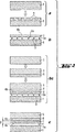
第1工程a)において、予め決められた形状の周期的に繰り返される空所2を有するパターンを、(図1および2に示されるように)半導体出発材料(基板)1の表面に、適当な場合は表面の部分に製造する。 In the first step a), a pattern having a periodically repeated void 2 of a predetermined shape is applied to the surface of the semiconductor starting material (substrate) 1 (as shown in FIGS. 1 and 2) In case it is manufactured on the surface part.
前記方法は所望の半導体材料に適用できるが、有利にはシリコン−ゲルマニウム、ヒ化ガリウム、炭化珪素およびインジウムリン化物、特に有利にシリコンに適用する。シリコンは半導体部品の製造に特に重要であるので、本発明の方法の利点および有利な態様をシリコンに関して説明するが、前記方法の適用はシリコンに限定されない。 The method can be applied to any desired semiconductor material, but is preferably applied to silicon-germanium, gallium arsenide, silicon carbide and indium phosphide, particularly preferably silicon. Since silicon is particularly important for the manufacture of semiconductor components, the advantages and advantageous aspects of the method of the present invention will be described with respect to silicon, but the application of the method is not limited to silicon.
基板は種々の材料の種類からなっていてもよく、半導体材料のフィルムまたは層が基板の表面層から形成されるので、表面に近い部分の形成は特に半導体層のその後の特性にかなりの影響を与える。 The substrate can be of various material types, and since the film or layer of semiconductor material is formed from the surface layer of the substrate, the formation of the portion near the surface has a significant effect on the subsequent properties of the semiconductor layer, in particular. give.
平坦な表面を有するウェーハの形の基板を使用することが有利である。以下の単結晶シリコンウェーハを使用することが特に有利である。所望のドーピングおよびコドーピングを有するCZウェーハまたはFZウェーハ(例えば窒素ドーピングウェーハ)(すなわちチョクラルスキー法または帯域浮遊法を使用して単結晶から製造されるウェーハ)、エピタキシャル層を備えたウェーハ、熱処理したウェーハおよび重大なボイドおよび格子間凝結物のない材料(ボイド不含シリコンまたはパーフェクトシリコン)または純粋なアイソトープシリコン(28Si)。 It is advantageous to use a substrate in the form of a wafer having a flat surface. It is particularly advantageous to use the following single crystal silicon wafers: CZ wafers or FZ wafers (eg, nitrogen doped wafers) having the desired doping and co-doping (ie, wafers made from single crystals using Czochralski or zone-floating methods), wafers with epitaxial layers, heat treatment Wafers and materials without significant voids and interstitial condensation (void-free silicon or perfect silicon) or pure isotope silicon ( 28 Si).
本発明の構成は、公知の研磨および両面研磨(DSP)した表面特性のほかに、鏡面研磨した(ヘイズ不含でない)ウェーハ、微細研磨したウェーハ、エッチングしたウェーハを使用することが可能であることにある。 The structure of the present invention can use a mirror-polished (not containing haze) wafer, a fine-polished wafer, and an etched wafer, in addition to the known polished and double-side polished (DSP) surface characteristics. It is in.
公知のフォトリソグラフィー法、マスクおよび露光技術、イオンビームエッチング、プラズマエッチングによるトレンチエッチングを使用して、レーザーまたは類似の方法を使用して(Silicon processing for the VLSI Era,S.Wolf,ISBN0−961672−16−1),工程a)で表面の近くの層に空所2(図1および2)を製造する。これらの空所(トレンチ)2の大きさは幅、直径、深さ、形状および間隔に関して正確に決められる。ホール、トレンチまたは他の規則的または不規則的幾何学的形状が可能であり、規則的な形が有利であり、実質的に円形または正方形のホールが特に有利である。 Using known photolithography methods, mask and exposure techniques, ion beam etching, trench etching by plasma etching, using laser or similar methods (Silicon processing for the VLSI Era, S. Wolf, ISBN 0-96167- 16-1), void 2 (FIGS. 1 and 2) is produced in a layer near the surface in step a). The size of these voids (trench) 2 is precisely determined with respect to width, diameter, depth, shape and spacing. Holes, trenches or other regular or irregular geometric shapes are possible, regular shapes are preferred, and substantially circular or square holes are particularly advantageous.
空所2を高い密度で表面の一部の領域にまたは有利に実質的に表面1の全部の表面に製造する。例として、ウェーハの形の基板の場合に、2つの基板の一方の実質的に全体に空所を備えることが有利である。予め決定された形状の周期的に繰り返される空所からなるパターンが形成されるように空所を製造する。この方法を継続して形成される半導体材料の層が所望の厚さDを得るように、空所の幾何学的寸法(すなわち主に横断面、深さおよび間隔)を選択する。この目的のために、直径(円形のホールの場合に)またはエッジ長さ(正方形のホールの場合に)を5D/5〜2D、特に有利にD/3〜Dに、トレンチ深さをD〜4Dにおよびトレンチ間隔をD/2〜3Dに選択することが有利である。
The cavities 2 are produced at a high density in a partial area of the surface or preferably on substantially the
空所の幾何学的寸法は、例えば工程b)の引き続く熱処理の間に空所から形成される個々の空洞3が結合してより大きい空洞3を形成できるように選択する。(図1および2に示される空洞は個々の空洞とより大きい空洞を表す。)この場合に空所を少ない数の正確に配置された位置におよびかなり大きい間隔で製造することが有利であり、工程b)の後に空洞3にウェブ3aがなお残る。
The geometric dimensions of the cavities are selected, for example, so that the
しかし有利にはすべて同じ形状であるホールを、規則的な、例えば正方形または六角形のパターンで、ホールからホールまでの間隔が一定で製造し、所定の位置でより大きい間隔を省くことが特に有利である。この場合にホールの幾何学的寸法およびホールからホールまでの間隔を、工程b)による熱処理の間に平滑層により表面が閉鎖するが、個々の空所から形成される個々の空洞が一緒に融合してより大きい空洞をまだ形成しないように有利に選択する。 However, it is particularly advantageous to produce holes that are all of the same shape in a regular, for example square or hexagonal pattern, with a constant hole-to-hole spacing and omit larger spacings in place. It is. In this case, the geometrical dimensions of the holes and the distance from hole to hole are closed by the smooth layer during the heat treatment according to step b), but the individual cavities formed from the individual cavities fuse together. Thus, it is advantageously chosen not to form a larger cavity yet.
引き続く工程b)で基板を熱処理し、原子の表面移動のために表面に接近する空所2を生じ、閉鎖した層4が形成され、同時に層の下に空洞3が形成される。この工程を継続して、空洞の上の層4は最後に半導体材料の層またはフィルムを形成する。
In a subsequent step b), the substrate is heat-treated, creating a cavity 2 that approaches the surface for the surface movement of atoms, forming a
工程a)およびb)に関する技術は、刊行物、ツナシマ、Y.サトウ、T.およびミズシマ、I.Electrochem.Soc.Proc.17(2000)532−545頁に記載されている。 Techniques for steps a) and b) are described in the publication, Tsunashima, Y. et al. Sato, T. and Mizushima, I. Electrochem. Soc. Proc. 17 (2000) 532-545.
工程a)で空所を製造した所に連続する空洞が形成され、空洞3の上の層4および基板1の残りが予め決められた間隔で意図的に構成されたウェブ3aにより一緒に保持されるように、工程b)を有利に調節する。工程a)で空所の間により大きい間隔が維持される位置にウェブが形成される。
A continuous cavity is formed where the void was produced in step a), and the
特に有利な選択である決められた位置により大きい間隔を有せずに工程a)で空所が製造される場合は、層4の表面が閉鎖されるが、個々の空所から形成される個々の空洞がなお互いに結合しないように工程b)の熱処理を調節する。図3は相当して処理したシリコンウェーハの表面の断面のSEM画像を示す。個々の空所から形成される個々の空洞3の層の上の閉鎖した層4が示される。
If the cavities are produced in step a) without having a larger spacing at a defined position, which is a particularly advantageous choice, the surface of the
個々の材料に依存して、200〜1500℃で3秒〜6時間の間熱処理を行い、この温度および継続時間はすでに説明したやり方で工程を調節するために使用される。熱処理を、半導体材料の表面に酸化物層(自然酸化物)の形成を阻止するすべての雰囲気で、有利には還元ガスまたはガス混合物または不活性ガスおよびガス混合物中で行うことができる。水素またはアルゴンまたは水素とアルゴンの混合物を有する雰囲気が有利である。熱処理を大気圧でまたは減圧で行うことができる。半導体材料の原子のできるだけ高い表面移動性が達成できるように処理条件を選択する。 Depending on the particular material, a heat treatment is carried out at 200-1500 ° C. for 3 seconds to 6 hours, this temperature and duration being used to adjust the process in the manner already described. The heat treatment can be carried out in any atmosphere that prevents the formation of an oxide layer (native oxide) on the surface of the semiconductor material, preferably in a reducing gas or gas mixture or inert gas and gas mixture. An atmosphere with hydrogen or argon or a mixture of hydrogen and argon is advantageous. The heat treatment can be performed at atmospheric pressure or at reduced pressure. Processing conditions are selected so that the highest possible surface mobility of the atoms of the semiconductor material can be achieved.
基板としてシリコンを使用する場合に、以下の設定条件で工程b)を実施する。温度700〜1370℃、有利に900〜1250℃、特に有利に950〜1150℃、圧力1〜100トル、有利に1〜50トル、特に有利に5〜20トル、時間3秒〜6時間、有利に1分〜30分。有利に水素またはアルゴンまたは2つのガスの混合物を有する非酸化雰囲気で熱処理を行う。
When silicon is used as the substrate, step b) is performed under the following setting conditions. Temperature 700 to 1370 ° C, preferably 900 to 1250 ° C, particularly preferably 950 to 1150 ° C,
工程b)で基板内の、特に空洞3の上のフィルムまたは層4内のCOPs(結晶配向ピット、ボイドの集合体)が同時にアニーリングされるように処理条件を有利に選択する。シリコンの場合に、これは、欧州特許第829559号または米国特許第5935320号に記載されるように、1000℃より高い温度を必要とする。
In step b), the processing conditions are advantageously selected so that the COPs (crystal orientation pits, a collection of voids) in the substrate, in particular on the
更にこの工程で温和な低エネルギーイオン衝撃により半導体材料の原子の表面の移動性を高めることができ、前記衝撃はより急速に空所を閉鎖しまたはより低い温度またはより短い時間の使用を可能にする。 In addition, this process can increase the mobility of the atomic surface of the semiconductor material by mild low energy ion bombardment, which can close the void more quickly or use at lower temperature or shorter time. To do.
熱処理のほかに、熱処理の一部としてまたは引き続く熱処理として、閉鎖した表面にエピタキシャル層を堆積することが可能である。これは、例えば処理時間を短縮することを可能にする。基板ウェーハの表面が、例えはボンディングに不利な作用を有する熱処理だけの後の、場合により引き続くボンディングのために十分に滑らかでない場合に、エピタキシャル層の堆積が有効である。空洞の形成に適している温度の範囲内で堆積温度が選択される条件で、0.5μm未満の厚さを有するエピタキシャル層が少ない表面均一性を有効に補償することは知られている(T.Bearda、P.Mertens、M.M.Heyns、R.Schmolke、Jpn.J.Appl.Phys.39(2000)L841;R.Schmolke、M.Blietz、R.Schauer、D.Zemke、H.Oelkrug、W.v.Ammon、U.Lambert、D.Graef、The electrochem.Soc.PV2000−17(2000)3)。この工程の組み合わせから得られ、目標厚さを上回ることを可能にする半導体材料の層は、全部の費用を考慮して、他の部分に記載される適当な引き続く熱処理を使用して再現可能な、制御されたやり方で大きさを減少することができる。 In addition to heat treatment, it is possible to deposit an epitaxial layer on the closed surface as part of the heat treatment or as a subsequent heat treatment. This makes it possible to shorten the processing time, for example. The deposition of the epitaxial layer is effective when the surface of the substrate wafer is not sufficiently smooth, for example after subsequent heat treatments which have an adverse effect on the bonding, and possibly for subsequent bonding. It is known that epitaxial layers having a thickness of less than 0.5 μm effectively compensate for low surface uniformity, provided that the deposition temperature is selected within a temperature range suitable for the formation of cavities (T Bearda, P. Mertens, MM Heyns, R. Schmolke, Jpn. J. Appl. Phys. 39 (2000) L841; W. v. Ammon, U. Lambert, D. Graef, The electrochem. Soc. PV2000-17 (2000) 3). The layer of semiconductor material obtained from this combination of steps and allowing the target thickness to be exceeded is reproducible using the appropriate subsequent heat treatment described elsewhere, considering the overall cost. The size can be reduced in a controlled manner.
製造すべき半導体材料のフィルムまたは層4はその少ない厚さのためにかなり低い機械的安定性を有する。従って空洞の層が製造された近くの基板の表面を他の工程bc)で、図2に示されるように、担体材料5の表面に結合する(ボンディング)することが有利である。担体材料は絶縁性固体であるかまたは少なくとも表面に絶縁層6を有する。使用される担体材料は、有利には炭化珪素、シリコン−ゲルマニウム、ヒ化ガリウム、石英、プラスチック。ガラス、またはセラミックからなる群から選択される。担体材料としてシリコンが特に有利である。シリコンの場合は、酸化珪素の絶縁層が表面で特に有利である。互いに結合する基板の表面および担体材料は同じ幾何学的寸法を有することが有利である。担体材料がウェーハの形で存在することも有利である。
The film or
担体材料はすでに組み込まれた内部ゲッターを有し、これが部品の製造中に導入された金属不純物を結合し、不純物を部品の活性領域から取り出す。 The support material has an internal getter already incorporated, which binds metal impurities introduced during the manufacture of the part and removes the impurities from the active area of the part.
半導体材料1および担体材料5を技術水準から公知の方法(Q.−Y.Tongand U.Goesele:Semiconductor wafer processing,ISBN0−471−57481−3)を使用して結合する。
The
最終工程c)で層またはフィルム4を基板1の残りから、特に空洞3の層に沿って分離する。これらの空洞のために、分離は、他の方法に比べて材料上できわめて温和である。分離は有利に熱により行い、この場合に分離を特に温和に行うように空洞が融合する。
In the final step c), the layer or
特に熱による分離の場合に、トレンチから形成される個々の小さい空洞が、この作業で基板ウェーハの機械的安定性を保証するために、結合中に完全に融合しなくてよい。個々の小さい空洞は結合工程の後または間に実施する熱工程で一緒に融合して最良の大きい空洞を形成する。この分離目的の第2熱工程は、基板がシリコンからなる場合に、800〜1370℃、有利に900〜1200℃の温度範囲で3秒〜4時間、有利に1〜30分の時間の熱処理を含む。例として垂直炉またはRTA装置(急速熱アニーリング用ランプ形炉)として知られているものを使用する。熱処理は大気圧または減圧で、所望のガス雰囲気、有利に還元または不活性ガス雰囲気、特に有利に水素またはアルゴンまたは水素とアルゴンの混合物を含む雰囲気で実施する。更なる均一化および薄い層の平滑性を達成するために、熱処理の時間を延長することが適当である。 In particular in the case of thermal isolation, the individual small cavities formed from the trenches do not have to be completely fused during bonding in order to ensure the mechanical stability of the substrate wafer in this operation. The individual small cavities are fused together in a thermal process performed after or during the bonding process to form the best large cavities. The second thermal process for the purpose of separation is a heat treatment in the temperature range of 800 to 1370 ° C., preferably 900 to 1200 ° C., for 3 seconds to 4 hours, preferably 1 to 30 minutes when the substrate is made of silicon. Including. By way of example, what is known as a vertical furnace or RTA apparatus (ramp furnace for rapid thermal annealing) is used. The heat treatment is carried out at atmospheric pressure or reduced pressure in the desired gas atmosphere, preferably a reducing or inert gas atmosphere, particularly preferably hydrogen or argon or an atmosphere comprising hydrogen or a mixture of hydrogen and argon. In order to achieve further uniformity and smoothness of the thin layer, it is appropriate to extend the time of the heat treatment.
しかし融合した空洞に沿って分離するために使用できる他の公知の方法も存在する。機械的方法の中で流体ジェットによる分離(サカグチ等、Solid State Technology43(6)(2000)88〜92頁)、せん断力の使用(Current等、Ultrashallow junctions or ultrathin SOI?,Solid State Technology,2000年9月)および音響分離法(超音波またはメガサウンドを使用する)を挙げるべきである。適当なガスまたは液体(フッ化水素酸または硝酸とフッ化水素酸の混合物)を使用するエッチングによる空洞の間に残ったウェブの除去による化学的分離も可能である。種々の分離法の組み合わせも可能である。 However, there are other known methods that can be used to separate along the fused cavity. Separation by fluid jet among mechanical methods (Sakaguchi et al., Solid State Technology 43 (6) (2000) pp. 88-92), use of shear force (Current et al., Ultrashallow junctions or ultrathin SOI ?, Solid State Tech 2000). September) and acoustic separation methods (using ultrasound or mega sound) should be mentioned. Chemical separation is also possible by removing the web left between the cavities by etching using a suitable gas or liquid (hydrofluoric acid or a mixture of nitric acid and hydrofluoric acid). A combination of various separation methods is also possible.
層またはフィルムの所望の目標厚さを達成できるので、エピタキシー反応器での半導体材料の表面へのエピタキシャル層の被覆と工程c)の組み合わせが有利である。 Since the desired target thickness of the layer or film can be achieved, the combination of coating of the epitaxial layer on the surface of the semiconductor material in an epitaxy reactor and step c) is advantageous.
本発明の方法はSOIパターンの製造に特に有利であることが示された。前記方法は、例えばるつぼ引き上げ単結晶から製造したシリコンウェーハ(CZウェーハ)を基板として使用することを可能にする。技術水準によりこれらはCOPsを生じ、これはシリコンウェーハに存在し、更にこれから製造されるSOIウェーハのシリコンの薄い層に存在し、部品の製造に問題を生じる。この理由から技術水準により、使用される基板ウェーハが帯域浮遊法を使用して、るつぼを使用せずに引き出した単結晶から製造したシリコンウェーハ(FZウェーハ)であることが有利である。この条件が認められない場合には、シリコンの薄い層のCOPsを、SOIウェーハの製造後に、有利に水素雰囲気での熱処理によりアニーリングしなければならない。これに対して本発明の方法では、工程b)で表面の熱による閉鎖の間に、COPsを同時にアニーリングできるので、基板ウェーハとして問題なくCZウェーハを使用することが可能であり、これが特に有利である。 The method of the present invention has been shown to be particularly advantageous for the production of SOI patterns. The method makes it possible to use, for example, a silicon wafer (CZ wafer) produced from a crucible pulling single crystal as a substrate. Depending on the state of the art, these give rise to COPs, which are present in the silicon wafer and also in the thin layer of silicon of the SOI wafers to be produced from this, causing problems in the production of the parts. For this reason, according to the state of the art, it is advantageous that the substrate wafer used is a silicon wafer (FZ wafer) manufactured from a single crystal drawn without using a crucible, using the zone floating method. If this condition is not observed, the thin layer of COPs of silicon must be annealed, preferably by heat treatment in a hydrogen atmosphere, after the manufacture of the SOI wafer. In contrast, in the method of the present invention, since COPs can be simultaneously annealed during the thermal closure of the surface in step b), it is possible to use CZ wafers without problems as substrate wafers, which is particularly advantageous. is there.
本発明の方法の他の利点は、工程b)で製造した空所の適当な配置および形状を使用することにより、50nm以下の厚さを有するきわめて薄いシリコン層を有するSOIウェーハを製造することが可能であるという事実にある。基本的に個々の空所の深さ/幅の比を維持しながら、製造されるシリコンウェーハを薄く、滑らかにし、空所の横断面を小さく、空所間の距離を短くすることが可能である。 Another advantage of the method of the present invention is that it makes it possible to produce SOI wafers with a very thin silicon layer having a thickness of 50 nm or less by using an appropriate arrangement and shape of the cavities produced in step b). In fact that is possible. While maintaining the depth / width ratio of individual cavities, it is possible to make the silicon wafers produced thinner and smoother, reduce the cross section of the cavities, and shorten the distance between the cavities. is there.
空所の幾何学的パラメーターと製造されるシリコンの薄い層の厚さの関係を、幾何学的パラメーターを変動することにより実験的に決定することができる。50nm未満の厚さ範囲に要求される周期的構造は、例えばナノインプリント法、電子ビームリソグラフィー、X線リソグラフィーまたは極端UVリソグラフィーにより達成することができる。将来は、フォトリソグラフィー分野でなされる進歩により(他の新しい方法が開発される)50nm以下の範囲でさえも高いレベルの正確性をもって周期的パターン化を実施することが可能になり、この種の薄い層の厚さの変動を5%未満に減少することができる。 The relationship between the void geometry parameter and the thickness of the thin layer of silicon produced can be determined experimentally by varying the geometry parameter. The periodic structure required for a thickness range of less than 50 nm can be achieved by, for example, nanoimprinting, electron beam lithography, X-ray lithography or extreme UV lithography. In the future, advances made in the field of photolithography (where other new methods will be developed) will make it possible to perform periodic patterning with a high level of accuracy even in the sub-50 nm range. Thin layer thickness variation can be reduced to less than 5%.
現在でも前記方法は10%以下、有利に5%以下および特に有利に1%以下の形状の許容性を有して幾何学的パターンを達成することができる。幾何学的パターンの許容性がきびしいほど、得られる層厚の均一性が良好になる。層厚の許容性は個々の幾何学的パターンの許容性より一般に低い。これは5%以下の層厚の均一性の達成を可能にする。 Even now, the method can achieve geometric patterns with a shape tolerance of 10% or less, preferably 5% or less and particularly preferably 1% or less. The tighter the tolerance of the geometric pattern, the better the resulting layer thickness uniformity. The tolerance of layer thickness is generally lower than that of individual geometric patterns. This makes it possible to achieve a layer thickness uniformity of 5% or less.
欠陥の実質的回避およびシリコンの薄い層の高い表面特性は複雑な他の処理工程を減少するかまたは完全に除去することを可能にし、これはSOIウェーハの製造に関するかなりの費用の減少を生じる。 The substantial avoidance of defects and the high surface properties of the thin layer of silicon allow complex other processing steps to be reduced or eliminated entirely, which results in a considerable cost reduction for the production of SOI wafers.
SOIウェーハを製造した後に、必要によりシリコン層4の厚さを調節、すなわち増加または減少することが可能である。層厚を増加するために、例えばシリコンのエピタキシャル層を堆積することが可能である。層厚の減少は公知の研磨法を使用して可能であるが、有利には気相エッチングまたは表面酸化および引き続く酸化珪素層の還元による除去を使用する。層厚の均一性が保持され、5%以下の層厚の均一性を有して20nm以下の層厚を得ることができる。
After the SOI wafer is manufactured, the thickness of the
引き続き必要により表面粗さを減少することも可能である。これは研磨工程または他の熱処理を含む。これは、有利には水素またはアルゴンまたは水素とアルゴンの混合物を有する還元雰囲気または不活性雰囲気で、大気圧または減圧で、1000〜1250℃の温度範囲で、10秒〜60分の間、バッチ炉またはランプ形炉(急速熱アニーリング炉、RTA)内で行う。バッチ炉は1行程当たり50〜250個のシリコンウェーハの積載量を有する垂直炉または水平炉である。RTAはカセットからカセットへの運転で1行程当たりそれぞれ1個のウェーハをアニーリングするランプ形炉である、
SOIウェーハの特に有利な特性は以下の本発明の方法の有利な実施態様により達成することができる。
It is also possible to reduce the surface roughness if necessary. This includes a polishing step or other heat treatment. This is preferably carried out in a reducing or inert atmosphere with hydrogen or argon or a mixture of hydrogen and argon, at atmospheric pressure or reduced pressure, at a temperature range of 1000 to 1250 ° C. for 10 seconds to 60 minutes, for a batch furnace. Alternatively, it is carried out in a lamp furnace (rapid thermal annealing furnace, RTA). The batch furnace is a vertical furnace or horizontal furnace having a load capacity of 50 to 250 silicon wafers per stroke. RTA is a lamp-type furnace that anneals one wafer each per stroke in a cassette-to-cassette operation.
Particularly advantageous properties of SOI wafers can be achieved by the following advantageous embodiments of the method of the invention.
基板ウェーハとしてFZウェーハを使用する場合に、ボイドを含まないだけでなく、BMDも含まないシリコンの薄い層を有するSOIウェーハを得ることが可能である。BMD(バルクミクロ欠陥)は酸素沈積物であり、ボイドは結晶空位の集合体である。 When an FZ wafer is used as a substrate wafer, it is possible to obtain an SOI wafer having a thin layer of silicon that does not contain voids but also does not contain BMD. BMD (bulk microdefects) are oxygen deposits, and voids are aggregates of crystal vacancies.
使用される基板ウェーハが窒素を多くドープしたCZウェーハである場合に、従来のCZウェーハに比べて高い滑り抵抗およびずれの形成を達成することが可能である。窒素を多くドープしたCZウェーハは1×10¹⁴〜5×10¹⁵/cm3の窒素含量を有するCZウェーハである。窒素を有しないCZウェーハに比べて窒素を多くドープしたウェーハは熱誘発性滑りおよびずれに対する著しく増加した抵抗および高いBMD密度(Graef等、ECS PB2000−17,319〜330頁、Ammon等、ECS PV
94−10、136頁、スエオカ等、ECS PV2000−17、164−179頁)を有する。
When the substrate wafer used is a nitrogen-doped CZ wafer, it is possible to achieve higher slip resistance and misalignment compared to conventional CZ wafers. A nitrogen-doped CZ wafer is a CZ wafer having a nitrogen content of 1 × 10 14 to 5 × 10 15 / cm 3 . Wafers rich in nitrogen compared to CZ wafers without nitrogen have significantly increased resistance to thermally induced slip and slip and high BMD density (Graef et al., ECS PB2000-17, pp. 319-330, Ammon et al., ECS PV
94-10, 136, Suoka et al., ECS PV2000-17, 164-179).
他の可能性は単結晶シリコンと異なる担体材料、例えば多結晶シリコン、ガラスまたはセラミックを使用することである。 Another possibility is to use a support material different from single crystal silicon, for example polycrystalline silicon, glass or ceramic.
本発明の方法は、複数の層またはフィルムを有するパターンの製造に特に有利に使用することができる。この目的のために、前記方法を少なくとも2回連続して実施し、第1工程の後に上に配置された半導体材料の第1層を有する担体材料を担体材料としてもう一度使用し、第1層に1個以上の他の層を被覆する。 The method according to the invention can be used particularly advantageously for the production of patterns having a plurality of layers or films. For this purpose, the method is carried out at least twice in succession, once again using a carrier material having a first layer of semiconductor material disposed thereon after the first step as a carrier material, One or more other layers are coated.
実施例
シリコンウェーハ1(図2)の滑らかな平坦な表面に本発明の方法のa)工程で周期的に繰り返される空所(トレンチ)を備えた。トレンチはエッジ長さ約0.5μmを有する正方形の横断面を有し、トレンチとトレンチの間隔は約0.9μmであった。トレンチは規則的な正方形のパターンで配置された。トレンチは技術水準により、トレンチの深さ3μmが得られるようにイオンビームエッチングにより製造した。
Example A cavity (trench) periodically repeated in step a) of the method of the present invention was provided on a smooth flat surface of a silicon wafer 1 (FIG. 2). The trench had a square cross section with an edge length of about 0.5 μm and the spacing between the trenches was about 0.9 μm. The trenches were arranged in a regular square pattern. The trench was manufactured by ion beam etching so as to obtain a trench depth of 3 μm according to the technical level.
引き続きシリコンウェーハ1のパターン化された表面を、工程b)で純粋水素雰囲気で、10トルの圧力下、水素流動速度10sccmおよび温度1100℃で10分間継続する熱処理により閉鎖した。処理中にトレンチ2から形成される空洞3がウェーハの閉鎖された表面4に平行に約0.25μmまで拡大した。図3は形成された空洞3およびその上の閉鎖された、完全な滑らかな層4のSEM写真を示す。この閉鎖された表面は、その滑らかさのために、図2による担体ウェーハに結合する(ボンディング)ために特に適している。
Subsequently, the patterned surface of the
工程b)で製造したシリコンウェーハを、引き続き他の工程bc)で、その表面4bにより、同様にシリコンからなり、酸化珪素の層6が備えられた担体材料5と、EVG、Schaerding、オーストリアにより製造された市販の結合剤を使用して結合した。
The silicon wafer produced in step b) is subsequently produced in another step bc) by means of its
工程c)で、酸化珪素層6を介して結合したシリコンウェーハを他の熱処理で処理した。この熱処理のために、工程b)で表面の閉鎖に使用した条件と同じ条件を選択した。この熱処理は図3に示される空洞3を一緒に融合し、連続する空洞7(図4)が形成され、図3で空洞3をなお包囲するシリコン層4を分離した。図4は新たに形成された基板シリコンウェーハ1の表面1aを示し、この上に連続する空洞7が存在し、空洞はシリコンウェーハ1から製造されたシリコンの薄い層4を完全に分離する。シリコンの薄い層4は担体シリコンウェーハ5の酸化物層6とのみ結合する(5および6は図面に示される)。層4の厚さは約1μmであり、層は基板1の残りの部分に軽く固定されて残る。基板の残りの部分の表面1aと異なり、分離されたシリコンの薄い層4の表面4aはすでにきわめて滑らかである。図4の中心は表面4aにあり、これは電子部品の製造に供給される。
In step c), the silicon wafer bonded via the
Claims (15)
a)半導体材料の表面に予め決められた形状の周期的に繰り返される空所を有するパターンを製造する工程
b)前記材料の表面の閉鎖された層の下に周期的に繰り返される空所を有する層が形成されるまで表面にパターン化された材料を熱処理する工程
c)空所層に沿って半導体材料の残りから表面の閉鎖された層を分離する工程
からなる半導体材料の皮膜または層を製造する方法。The following steps:
a) producing a pattern having a periodically repeated void of a predetermined shape on the surface of the semiconductor material b) having a periodically repeated void under a closed layer of the surface of the material Heat treating the material patterned on the surface until a layer is formed c) producing a film or layer of semiconductor material comprising the step of separating the closed layer of the surface from the rest of the semiconductor material along the void layer how to.
Applications Claiming Priority (2)
| Application Number | Priority Date | Filing Date | Title |
|---|---|---|---|
| DE10131249A DE10131249A1 (en) | 2001-06-28 | 2001-06-28 | Production of a film or a layer of semiconductor material comprises producing structures of repeating recesses on the surface of a semiconductor material |
| PCT/EP2002/007125 WO2003003430A2 (en) | 2001-06-28 | 2002-06-27 | Film or layer made of semi-conductive material and method for producing said film or layer |
Publications (3)
| Publication Number | Publication Date |
|---|---|
| JP2004533726A JP2004533726A (en) | 2004-11-04 |
| JP2004533726A5 JP2004533726A5 (en) | 2005-09-02 |
| JP4331593B2 true JP4331593B2 (en) | 2009-09-16 |
Family
ID=7689811
Family Applications (1)
| Application Number | Title | Priority Date | Filing Date |
|---|---|---|---|
| JP2003509512A Expired - Lifetime JP4331593B2 (en) | 2001-06-28 | 2002-06-27 | Film or layer comprising semiconductor material and method for producing film or layer |
Country Status (9)
| Country | Link |
|---|---|
| US (2) | US7052948B2 (en) |
| EP (2) | EP1626440B1 (en) |
| JP (1) | JP4331593B2 (en) |
| KR (1) | KR100587997B1 (en) |
| CN (1) | CN100372060C (en) |
| AT (1) | ATE324670T1 (en) |
| DE (3) | DE10131249A1 (en) |
| TW (1) | TW575910B (en) |
| WO (1) | WO2003003430A2 (en) |
Families Citing this family (43)
| Publication number | Priority date | Publication date | Assignee | Title |
|---|---|---|---|---|
| JP4277481B2 (en) * | 2002-05-08 | 2009-06-10 | 日本電気株式会社 | Semiconductor substrate manufacturing method and semiconductor device manufacturing method |
| JP2004039735A (en) * | 2002-07-01 | 2004-02-05 | Fujitsu Ltd | Semiconductor substrate and its manufacturing method |
| EP2280412A3 (en) * | 2002-11-29 | 2011-02-16 | STMicroelectronics S.r.l. | Semiconductor substrate comprising at least a buried insulating cavity |
| TW582099B (en) * | 2003-03-13 | 2004-04-01 | Ind Tech Res Inst | Method of adhering material layer on transparent substrate and method of forming single crystal silicon on transparent substrate |
| DE10326578B4 (en) * | 2003-06-12 | 2006-01-19 | Siltronic Ag | Process for producing an SOI disk |
| DE10336271B4 (en) * | 2003-08-07 | 2008-02-07 | Siltronic Ag | Silicon wafer and process for its production |
| KR100605497B1 (en) * | 2003-11-27 | 2006-07-28 | 삼성전자주식회사 | Methods of forming SOI substrates, methods of fabricating semiconductor devices using the same, and semiconductor devices fabricated using the same |
| EP1577656B1 (en) | 2004-03-19 | 2010-06-09 | STMicroelectronics Srl | Method for manufacturing a semiconductor pressure sensor |
| JP4626175B2 (en) * | 2004-04-09 | 2011-02-02 | 株式会社Sumco | Manufacturing method of SOI substrate |
| DE102004021113B4 (en) * | 2004-04-29 | 2006-04-20 | Siltronic Ag | SOI disk and process for its production |
| DE102004030612B3 (en) | 2004-06-24 | 2006-04-20 | Siltronic Ag | Semiconductor substrate and method for its production |
| US20100117152A1 (en) * | 2007-06-28 | 2010-05-13 | Chang-Woo Oh | Semiconductor devices |
| KR100843717B1 (en) * | 2007-06-28 | 2008-07-04 | 삼성전자주식회사 | Semiconductor device having floating body device and bulk body device and methods of fabricating the same |
| KR100555569B1 (en) | 2004-08-06 | 2006-03-03 | 삼성전자주식회사 | Semiconductor device having the channel area restricted by insulating film and method of fabrication using the same |
| DE102004041378B4 (en) * | 2004-08-26 | 2010-07-08 | Siltronic Ag | Semiconductor wafer with a layered structure with low warp and bow and process for its production |
| DE602004010117D1 (en) * | 2004-09-16 | 2007-12-27 | St Microelectronics Srl | Process for the production of compacted semiconductor wafers by means of layer transfer |
| DE102004054564B4 (en) * | 2004-11-11 | 2008-11-27 | Siltronic Ag | Semiconductor substrate and method for its production |
| DE102004062356A1 (en) * | 2004-12-23 | 2006-07-13 | Siltronic Ag | Semiconductor wafer with a semiconductor layer and an underlying electrically insulating layer and method for their preparation |
| DE102005000826A1 (en) | 2005-01-05 | 2006-07-20 | Siltronic Ag | Semiconductor wafer with silicon-germanium layer and method for its production |
| FR2884647B1 (en) * | 2005-04-15 | 2008-02-22 | Soitec Silicon On Insulator | TREATMENT OF SEMICONDUCTOR PLATES |
| EP1719993A1 (en) * | 2005-05-06 | 2006-11-08 | STMicroelectronics S.r.l. | Integrated differential pressure sensor and manufacturing process thereof |
| CN1312328C (en) * | 2005-05-16 | 2007-04-25 | 浙江大学 | Methd for preparing monocrystalline silicon nano membrane for nano photon technique |
| US7629209B2 (en) * | 2005-10-17 | 2009-12-08 | Chunghwa Picture Tubes, Ltd. | Methods for fabricating polysilicon film and thin film transistors |
| JP4342503B2 (en) * | 2005-10-20 | 2009-10-14 | 富士通マイクロエレクトロニクス株式会社 | Semiconductor device and inspection method of semiconductor device |
| KR101171189B1 (en) * | 2005-10-21 | 2012-08-06 | 삼성전자주식회사 | Dummy glass substrate and making method of display apparatus |
| FR2895563B1 (en) * | 2005-12-22 | 2008-04-04 | Soitec Silicon On Insulator | METHOD FOR SIMPLIFYING A FINISHING SEQUENCE AND STRUCTURE OBTAINED BY THE METHOD |
| US7799640B2 (en) * | 2006-09-28 | 2010-09-21 | Semiconductor Components Industries, Llc | Method of forming a semiconductor device having trench charge compensation regions |
| KR100882932B1 (en) | 2007-06-11 | 2009-02-10 | 삼성전자주식회사 | Semiconductor substrate and method of fabricating the same, method of fabricating semiconductor device and method of fabricating image sensor |
| US20090280588A1 (en) * | 2008-05-06 | 2009-11-12 | Leo Mathew | Method of forming an electronic device including removing a differential etch layer |
| EP2161741B1 (en) * | 2008-09-03 | 2014-06-11 | Soitec | Method for fabricating a semiconductor on insulator substrate with reduced SECCO defect density |
| US20100187572A1 (en) * | 2009-01-26 | 2010-07-29 | Cho Hans S | Suspended mono-crystalline structure and method of fabrication from a heteroepitaxial layer |
| DE102009030298B4 (en) | 2009-06-24 | 2012-07-12 | Siltronic Ag | Process for local polishing of a semiconductor wafer |
| JP5585056B2 (en) * | 2009-11-19 | 2014-09-10 | 富士電機株式会社 | SON semiconductor substrate manufacturing method |
| JP5891597B2 (en) * | 2011-04-07 | 2016-03-23 | 富士電機株式会社 | Manufacturing method of semiconductor substrate or semiconductor device |
| CN102294655A (en) * | 2011-08-10 | 2011-12-28 | 开化美盛电子科技有限公司 | Manufacturing method for carrier used for cementing silicon rods |
| US9406551B2 (en) | 2012-09-27 | 2016-08-02 | Infineon Technologies Austria Ag | Method for manufacturing a semiconductor substrate, and method for manufacturing semiconductor devices integrated in a semiconductor substrate |
| DE102015209889B4 (en) | 2015-05-29 | 2018-12-06 | Siltronic Ag | Structured semiconductor wafer and method for its production |
| US10833175B2 (en) * | 2015-06-04 | 2020-11-10 | International Business Machines Corporation | Formation of dislocation-free SiGe finFET using porous silicon |
| CN109313154B (en) * | 2016-08-03 | 2022-01-18 | 惠普发展公司,有限责任合伙企业 | Conductor arranged in a layer |
| DE102019106124A1 (en) | 2018-03-22 | 2019-09-26 | Infineon Technologies Ag | Forming semiconductor devices in silicon carbide |
| US10943813B2 (en) | 2018-07-13 | 2021-03-09 | Globalwafers Co., Ltd. | Radio frequency silicon on insulator wafer platform with superior performance, stability, and manufacturability |
| FR3091000B1 (en) * | 2018-12-24 | 2020-12-04 | Soitec Silicon On Insulator | PROCESS FOR MANUFACTURING A SUBSTRATE FOR A FRONT FACE TYPE IMAGE SENSOR |
| US11710656B2 (en) * | 2019-09-30 | 2023-07-25 | Taiwan Semiconductor Manufacturing Company, Ltd. | Method of forming semiconductor-on-insulator (SOI) substrate |
Family Cites Families (26)
| Publication number | Priority date | Publication date | Assignee | Title |
|---|---|---|---|---|
| FR2681472B1 (en) * | 1991-09-18 | 1993-10-29 | Commissariat Energie Atomique | PROCESS FOR PRODUCING THIN FILMS OF SEMICONDUCTOR MATERIAL. |
| JP2901031B2 (en) * | 1992-01-30 | 1999-06-02 | キヤノン株式会社 | Semiconductor substrate and method of manufacturing the same |
| EP1043768B1 (en) | 1992-01-30 | 2004-09-08 | Canon Kabushiki Kaisha | Process for producing semiconductor substrates |
| US5427055A (en) * | 1992-01-31 | 1995-06-27 | Canon Kabushiki Kaisha | Method for controlling roughness on surface of monocrystal |
| FR2715503B1 (en) * | 1994-01-26 | 1996-04-05 | Commissariat Energie Atomique | Substrate for integrated components comprising a thin layer and its production method. |
| CN1132223C (en) * | 1995-10-06 | 2003-12-24 | 佳能株式会社 | Semiconductor substrate and producing method thereof |
| FR2748851B1 (en) * | 1996-05-15 | 1998-08-07 | Commissariat Energie Atomique | PROCESS FOR PRODUCING A THIN FILM OF SEMICONDUCTOR MATERIAL |
| DE19637182A1 (en) | 1996-09-12 | 1998-03-19 | Wacker Siltronic Halbleitermat | Process for the production of silicon wafers with low defect density |
| SG65697A1 (en) * | 1996-11-15 | 1999-06-22 | Canon Kk | Process for producing semiconductor article |
| US6155909A (en) * | 1997-05-12 | 2000-12-05 | Silicon Genesis Corporation | Controlled cleavage system using pressurized fluid |
| EP0895282A3 (en) * | 1997-07-30 | 2000-01-26 | Canon Kabushiki Kaisha | Method of preparing a SOI substrate by using a bonding process, and SOI substrate produced by the same |
| JP3324469B2 (en) | 1997-09-26 | 2002-09-17 | 信越半導体株式会社 | Method for producing SOI wafer and SOI wafer produced by this method |
| JP3472171B2 (en) * | 1997-12-26 | 2003-12-02 | キヤノン株式会社 | Semiconductor substrate etching method and etching apparatus, and semiconductor substrate manufacturing method using the same |
| JP3697106B2 (en) * | 1998-05-15 | 2005-09-21 | キヤノン株式会社 | Method for manufacturing semiconductor substrate and method for manufacturing semiconductor thin film |
| JP3618254B2 (en) * | 1998-06-02 | 2005-02-09 | 信越半導体株式会社 | Manufacturing method of SOI substrate |
| JP3762144B2 (en) * | 1998-06-18 | 2006-04-05 | キヤノン株式会社 | Method for manufacturing SOI substrate |
| TW465101B (en) * | 1998-09-04 | 2001-11-21 | Canon Kk | Semiconductor substrate and method for producing the same |
| CN1249531A (en) * | 1998-09-04 | 2000-04-05 | 佳能株式会社 | Process for mfg. semiconductor substrate |
| JP2000188269A (en) * | 1998-10-16 | 2000-07-04 | Canon Inc | Method for separating members, separation device and manufacture of substrate |
| JP2000124092A (en) * | 1998-10-16 | 2000-04-28 | Shin Etsu Handotai Co Ltd | Manufacture of soi wafer by hydrogen-ion implantation stripping method and soi wafer manufactured thereby |
| JP3453544B2 (en) * | 1999-03-26 | 2003-10-06 | キヤノン株式会社 | Manufacturing method of semiconductor member |
| US6326279B1 (en) * | 1999-03-26 | 2001-12-04 | Canon Kabushiki Kaisha | Process for producing semiconductor article |
| JP4074051B2 (en) * | 1999-08-31 | 2008-04-09 | 株式会社東芝 | Semiconductor substrate and manufacturing method thereof |
| JP3994602B2 (en) * | 1999-11-12 | 2007-10-24 | 信越半導体株式会社 | Silicon single crystal wafer, manufacturing method thereof, and SOI wafer |
| US6660606B2 (en) * | 2000-09-29 | 2003-12-09 | Canon Kabushiki Kaisha | Semiconductor-on-insulator annealing method |
| US6489217B1 (en) * | 2001-07-03 | 2002-12-03 | Maxim Integrated Products, Inc. | Method of forming an integrated circuit on a low loss substrate |
-
2001
- 2001-06-28 DE DE10131249A patent/DE10131249A1/en not_active Withdrawn
-
2002
- 2002-06-27 AT AT02758281T patent/ATE324670T1/en not_active IP Right Cessation
- 2002-06-27 US US10/481,537 patent/US7052948B2/en not_active Expired - Lifetime
- 2002-06-27 JP JP2003509512A patent/JP4331593B2/en not_active Expired - Lifetime
- 2002-06-27 CN CNB028131630A patent/CN100372060C/en not_active Expired - Lifetime
- 2002-06-27 EP EP05021844A patent/EP1626440B1/en not_active Expired - Lifetime
- 2002-06-27 DE DE50211238T patent/DE50211238D1/en not_active Expired - Lifetime
- 2002-06-27 TW TW91114122A patent/TW575910B/en not_active IP Right Cessation
- 2002-06-27 WO PCT/EP2002/007125 patent/WO2003003430A2/en active IP Right Grant
- 2002-06-27 KR KR1020037016800A patent/KR100587997B1/en active IP Right Grant
- 2002-06-27 DE DE50206581T patent/DE50206581D1/en not_active Expired - Lifetime
- 2002-06-27 EP EP02758281A patent/EP1402567B1/en not_active Expired - Lifetime
-
2006
- 2006-03-20 US US11/384,887 patent/US7417297B2/en not_active Expired - Lifetime
Also Published As
| Publication number | Publication date |
|---|---|
| EP1402567A2 (en) | 2004-03-31 |
| WO2003003430A3 (en) | 2003-03-20 |
| KR20040015282A (en) | 2004-02-18 |
| KR100587997B1 (en) | 2006-06-08 |
| US7052948B2 (en) | 2006-05-30 |
| US20060202310A1 (en) | 2006-09-14 |
| TW575910B (en) | 2004-02-11 |
| DE10131249A1 (en) | 2002-05-23 |
| EP1626440A1 (en) | 2006-02-15 |
| WO2003003430A2 (en) | 2003-01-09 |
| CN100372060C (en) | 2008-02-27 |
| US20040142542A1 (en) | 2004-07-22 |
| JP2004533726A (en) | 2004-11-04 |
| US7417297B2 (en) | 2008-08-26 |
| EP1626440B1 (en) | 2007-11-14 |
| CN1522461A (en) | 2004-08-18 |
| EP1402567B1 (en) | 2006-04-26 |
| ATE324670T1 (en) | 2006-05-15 |
| DE50211238D1 (en) | 2007-12-27 |
| DE50206581D1 (en) | 2006-06-01 |
Similar Documents
| Publication | Publication Date | Title |
|---|---|---|
| JP4331593B2 (en) | Film or layer comprising semiconductor material and method for producing film or layer | |
| US6313014B1 (en) | Semiconductor substrate and manufacturing method of semiconductor substrate | |
| US6054363A (en) | Method of manufacturing semiconductor article | |
| US6350703B1 (en) | Semiconductor substrate and production method thereof | |
| US6613678B1 (en) | Process for manufacturing a semiconductor substrate as well as a semiconductor thin film, and multilayer structure | |
| US6593173B1 (en) | Low defect density, thin-layer, SOI substrates | |
| US6461939B1 (en) | SOI wafers and methods for producing SOI wafer | |
| EP0843346B1 (en) | Method of manufacturing a semiconductor article | |
| US7582540B2 (en) | Method for manufacturing SOI wafer | |
| TWI344667B (en) | ||
| US7947571B2 (en) | Method for fabricating a semiconductor on insulator substrate with reduced Secco defect density | |
| TW201009904A (en) | Method of producing bonded wafer | |
| JP4631347B2 (en) | Partial SOI substrate and manufacturing method thereof | |
| JP4427777B2 (en) | Manufacturing method of semiconductor substrate | |
| JP2004281805A (en) | Flattening process method for semiconductor wafer | |
| JP4442090B2 (en) | Manufacturing method of SOI substrate | |
| JP2004288790A (en) | Soi substrate and method for manufacturing same | |
| JP2004214399A (en) | Manufacturing method for semiconductor substrate and wafer peeling-heat treatment apparatus | |
| WO2009106915A1 (en) | Method for reducing the amount or eliminating the crystalline defects, in a semiconductor layer of a composite structure | |
| JP2002176155A (en) | Method for manufacturing laminated soi wafer |
Legal Events
| Date | Code | Title | Description |
|---|---|---|---|
| A977 | Report on retrieval |
Free format text: JAPANESE INTERMEDIATE CODE: A971007 Effective date: 20061117 |
|
| A131 | Notification of reasons for refusal |
Free format text: JAPANESE INTERMEDIATE CODE: A131 Effective date: 20080125 |
|
| A521 | Request for written amendment filed |
Free format text: JAPANESE INTERMEDIATE CODE: A523 Effective date: 20080425 |
|
| A02 | Decision of refusal |
Free format text: JAPANESE INTERMEDIATE CODE: A02 Effective date: 20090123 |
|
| A521 | Request for written amendment filed |
Free format text: JAPANESE INTERMEDIATE CODE: A523 Effective date: 20090317 |
|
| A911 | Transfer to examiner for re-examination before appeal (zenchi) |
Free format text: JAPANESE INTERMEDIATE CODE: A911 Effective date: 20090422 |
|
| TRDD | Decision of grant or rejection written | ||
| A01 | Written decision to grant a patent or to grant a registration (utility model) |
Free format text: JAPANESE INTERMEDIATE CODE: A01 Effective date: 20090520 |
|
| A01 | Written decision to grant a patent or to grant a registration (utility model) |
Free format text: JAPANESE INTERMEDIATE CODE: A01 |
|
| A61 | First payment of annual fees (during grant procedure) |
Free format text: JAPANESE INTERMEDIATE CODE: A61 Effective date: 20090618 |
|
| R150 | Certificate of patent or registration of utility model |
Ref document number: 4331593 Country of ref document: JP Free format text: JAPANESE INTERMEDIATE CODE: R150 Free format text: JAPANESE INTERMEDIATE CODE: R150 |
|
| FPAY | Renewal fee payment (event date is renewal date of database) |
Free format text: PAYMENT UNTIL: 20120626 Year of fee payment: 3 |
|
| FPAY | Renewal fee payment (event date is renewal date of database) |
Free format text: PAYMENT UNTIL: 20130626 Year of fee payment: 4 |
|
| R250 | Receipt of annual fees |
Free format text: JAPANESE INTERMEDIATE CODE: R250 |
|
| R250 | Receipt of annual fees |
Free format text: JAPANESE INTERMEDIATE CODE: R250 |
|
| R250 | Receipt of annual fees |
Free format text: JAPANESE INTERMEDIATE CODE: R250 |
|
| R250 | Receipt of annual fees |
Free format text: JAPANESE INTERMEDIATE CODE: R250 |
|
| R250 | Receipt of annual fees |
Free format text: JAPANESE INTERMEDIATE CODE: R250 |
|
| R250 | Receipt of annual fees |
Free format text: JAPANESE INTERMEDIATE CODE: R250 |
|
| R250 | Receipt of annual fees |
Free format text: JAPANESE INTERMEDIATE CODE: R250 |
|
| R250 | Receipt of annual fees |
Free format text: JAPANESE INTERMEDIATE CODE: R250 |
|
| R250 | Receipt of annual fees |
Free format text: JAPANESE INTERMEDIATE CODE: R250 |
|
| R250 | Receipt of annual fees |
Free format text: JAPANESE INTERMEDIATE CODE: R250 |
|
| R250 | Receipt of annual fees |
Free format text: JAPANESE INTERMEDIATE CODE: R250 |
|
| EXPY | Cancellation because of completion of term |