JP4331060B2 - Organic thin film and manufacturing method thereof, optical recording medium using the thin film, and recording / reproducing method - Google Patents
Organic thin film and manufacturing method thereof, optical recording medium using the thin film, and recording / reproducing method Download PDFInfo
- Publication number
- JP4331060B2 JP4331060B2 JP2004184759A JP2004184759A JP4331060B2 JP 4331060 B2 JP4331060 B2 JP 4331060B2 JP 2004184759 A JP2004184759 A JP 2004184759A JP 2004184759 A JP2004184759 A JP 2004184759A JP 4331060 B2 JP4331060 B2 JP 4331060B2
- Authority
- JP
- Japan
- Prior art keywords
- thin film
- organic thin
- polymer
- recording medium
- copolymer
- Prior art date
- Legal status (The legal status is an assumption and is not a legal conclusion. Google has not performed a legal analysis and makes no representation as to the accuracy of the status listed.)
- Expired - Fee Related
Links
Images

Landscapes
- Thermal Transfer Or Thermal Recording In General (AREA)
- Moulding By Coating Moulds (AREA)
- Paints Or Removers (AREA)
- Optical Record Carriers And Manufacture Thereof (AREA)
- Optical Recording Or Reproduction (AREA)
- Manufacturing Optical Record Carriers (AREA)
Description
本発明は、電子的性質、導電的性質、光学的性質、磁気的性質などの新たな機能を発揮する機能性複合材料からなる有機薄膜とその製造方法、および該有機薄膜を記録層として用いた光記録媒体、ならびにその記録・再生方法に関する。 The present invention uses an organic thin film composed of a functional composite material that exhibits new functions such as electronic properties, conductive properties, optical properties, and magnetic properties, a manufacturing method thereof, and the organic thin film as a recording layer. The present invention relates to an optical recording medium and a recording / reproducing method thereof.
サブミクロンサイズで規則的に並んだ機能性複合材料を作製する方法は、電子的性質、導電的性質、光学的性質、磁気的性質等の新たな機能を発揮する材料を得る場合において重要な技術である。
このような機能性材料として、従来から金属ナノクラスターなどの金属超微粒子を用いた、いわゆる金属−有機複合材料の研究開発は進められている。しかしながら、無限の材料自由度と機能性が期待できるサブミクロンサイズの機能性有機材料と高分子材料との複合材料に関する研究開発はほとんど進められていないのが現状である。
The method of producing functional composite materials regularly arranged in submicron size is an important technology in obtaining materials that exhibit new functions such as electronic properties, conductive properties, optical properties, magnetic properties, etc. It is.
As such a functional material, research and development of a so-called metal-organic composite material using metal ultrafine particles such as metal nanoclusters has been advanced. However, there is almost no research and development on composite materials of submicron functional organic materials and polymer materials that can be expected to have unlimited material flexibility and functionality.
一方、光情報記録の分野では、CD規格、DVD規格に対応した記録が可能な、基板上に反射層を有する光記録媒体、例えば、CD−RやDVD−Rなどが商品化されている。このような光記録媒体では、今後さらに記録容量向上と小型化、記録密度の向上が求められており、その対策が必要とされている。 On the other hand, in the field of optical information recording, optical recording media having a reflective layer on a substrate, such as CD-R and DVD-R, which can be recorded in accordance with the CD standard and the DVD standard, are commercialized. In such an optical recording medium, further improvement in recording capacity, size reduction, and improvement in recording density are required in the future, and countermeasures are required.
現行システムにおける記録容量向上のための要素技術としては、記録ピットの微小化技術とMPEG2に代表される画像圧縮技術がある。記録ピットの微小化技術には、記録・再生光の短波長化や光学系の開口数NAの増大化が検討されているが、この方法では回折限界を超える記録・再生は不可能である。
そこで最近、回折限界を超えた記録・再生を可能とする超解像技術や近接場光を利用した光記録媒体、ならびにそのシステムに関して研究、開発されているが、未だ実用化には至っていないのが現状である。
Elemental techniques for improving the recording capacity in the current system include a recording pit miniaturization technique and an image compression technique represented by MPEG2. For recording pit miniaturization techniques, it has been studied to shorten the wavelength of recording / reproducing light and increase the numerical aperture NA of the optical system, but this method cannot perform recording / reproducing exceeding the diffraction limit.
Therefore, recently, research and development have been conducted on super-resolution technology that enables recording / reproduction exceeding the diffraction limit, optical recording media using near-field light, and their systems, but they have not yet been put into practical use. Is the current situation.
これらの課題に対処するため、本発明者らは先に、二次元方向に規則的に形成されたサブミクロンサイズのパターンからなる格子状構造を持つポリマー(例えば、ポリイオンコンプレックス)と、その格子状構造の孔の部分に機能性色素を埋設してサブミクロンサイズで規則的に配列して構成した有機薄膜とその製造方法、ならびにそれを用いた光記録媒体を提案した(例えば、特許文献1参照。)。
さらに、ポリマー薄膜形成時の環境(温度、湿度、空気の流れ、基板の傾斜など)による影響を回避して、二次元に規則的な格子状構造の再現性や均一性を向上させる方法(例えば、特許文献2参照。)や、格子状構造の再現性や均一性を向上させつつ、機能性色素サイズのバラツキを改善する方法(例えば、特許文献3参照。)について提案した。
In order to cope with these problems, the present inventors have previously described a polymer (for example, a polyion complex) having a lattice structure composed of submicron-sized patterns regularly formed in a two-dimensional direction, and the lattice shape. An organic thin film composed of functional dyes embedded in pores of the structure and regularly arranged in a submicron size, a manufacturing method thereof, and an optical recording medium using the organic thin film have been proposed (for example, see Patent Document 1). .)
Furthermore, avoiding the influence of the environment (temperature, humidity, air flow, substrate tilt, etc.) when forming the polymer thin film, and improving the reproducibility and uniformity of the two-dimensional regular lattice structure (for example, And Patent Document 2) and a method for improving the variation in the size of the functional dye while improving the reproducibility and uniformity of the lattice structure (for example, see Patent Document 3).
上記方法において、例えば、ポリイオンコンプレックスを用いた場合、ポリマー構造体の二次元方向における格子状構造の再現性や均一性、あるいは機能性色素サイズなどの一定の向上は図れるが、電子的性質、導電的性質、光学的性質、磁気的性質などの新たな機能を充分に発揮できる有機薄膜としては、さらに格子状構造の再現性や均一性の向上が必要とされている。特に、有機薄膜を用いた光記録媒体とする場合、エラー発生が少なく低エラー率で、良好な記録・再生信号を得るには、前記格子状構造の孔の部分に埋設された機能性部位の機能性色素サイズにバラツキがない有機薄膜であることが求められている。 In the above method, for example, when a polyion complex is used, the reproducibility and uniformity of the lattice structure in the two-dimensional direction of the polymer structure can be improved, or the functional dye size can be improved to a certain degree. Organic thin films that can sufficiently exhibit new functions such as optical properties, optical properties, and magnetic properties are required to further improve the reproducibility and uniformity of the lattice structure. In particular, in the case of an optical recording medium using an organic thin film, in order to obtain a good recording / reproducing signal with low error rate and low error rate, the functional portion embedded in the hole portion of the lattice structure is used. There is a demand for an organic thin film having no variation in functional dye size.
本発明は、上記従来技術に鑑みてなされたものであり、二次元方向に規則的に形成された格子状構造、すなわち格子状のパターンを有するポリマー構造体と、その格子状パターンの孔内に機能性部位として埋設された機能性材料とから構成される有機薄膜において、その格子状パターンと光機能性部位の再現性が高く、サイズの均一性に優れ、機能性材料がサブミクロンサイズで規則的に配列し、電子的性質、導電的性質、光学的性質、磁気的性質などの新たな機能を充分に発揮できる有機薄膜と、その製造方法を提供することを目的とする。
また、有機薄膜を利用することにより、ピットザイズの均一性が高く、ピックアップレンズの回折限界を超えた記録密度の記録・再生が可能で、かつエラー発生が少なく記録・再生信号の優れた光記録媒体と、その記録・再生方法を提供することを目的とする。
The present invention has been made in view of the above prior art, and has a lattice structure regularly formed in a two-dimensional direction, that is, a polymer structure having a lattice pattern, and the holes in the lattice pattern. Organic thin films composed of functional materials embedded as functional sites have high reproducibility of the lattice pattern and optical functional sites, excellent size uniformity, and functional materials are sub-micron-sized and ordered. It is an object of the present invention to provide an organic thin film that can be arranged in order and can fully exhibit new functions such as electronic properties, conductive properties, optical properties, magnetic properties, and the like, and a method for producing the same.
In addition, by using an organic thin film, optical recording with excellent pit size uniformity, recording / reproduction with a recording density exceeding the diffraction limit of the pickup lens, and excellent recording / reproduction signals with few errors. It is an object to provide a medium and a recording / reproducing method thereof.
すなわち、本発明は、二次元方向に規則的な格子状のパターンを有するポリマー構造体と、該格子状パターンの孔内に埋設された機能性材料とから構成される有機薄膜において、
前記ポリマーが、疎水性有機溶媒に可溶なブロック重合体と難溶なブロック重合体との共重合体からなり、該疎水性有機溶媒に可溶なブロック重合体がポリスチレンであり、かつ該ポリスチレンの共重合体に占める割合(体積比)が90vol%以上であることを特徴とする有機薄膜である。
ここで、上記機能性材料として機能性色素を用いることができる。また、上記有機薄膜を基板上に設けることができる。
That is, the present invention provides an organic thin film composed of a polymer structure having a regular lattice pattern in a two-dimensional direction and a functional material embedded in the holes of the lattice pattern.
The polymer comprises a copolymer of a block polymer soluble in a hydrophobic organic solvent and a block polymer hardly soluble, and the block polymer soluble in the hydrophobic organic solvent is polystyrene, and the polystyrene The organic thin film is characterized in that the proportion (volume ratio) in the copolymer is 90 vol% or more.
Here, a functional dye can be used as the functional material. Moreover, the said organic thin film can be provided on a board | substrate.
また、本発明は、基板上に、疎水性有機溶媒に可溶なブロック重合体と難溶なブロック重合体との共重合体からなり、該疎水性有機溶媒に可溶なブロック重合体がポリスチレンで、かつ該ポリスチレンの共重合体に占める割合(体積比)が90vol%以上であるポリマーの疎水性有機溶媒溶液をキャストして、二次元方向に規則的な格子状のパターンからなるポリマー構造体を形成し、さらにその上から機能性材料溶液をキャストして、前記格子状パターンの孔内に機能性材料を埋設することを特徴とする有機薄膜の製造方法に係るものである。 The present invention also comprises a copolymer of a block polymer soluble in a hydrophobic organic solvent and a hardly soluble block polymer on a substrate, wherein the block polymer soluble in the hydrophobic organic solvent is polystyrene. And a polymer structure having a regular lattice pattern in a two-dimensional direction by casting a hydrophobic organic solvent solution of a polymer having a proportion (volume ratio) of 90% by volume or more in the polystyrene copolymer And a functional material solution is cast from above, and the functional material is embedded in the holes of the lattice pattern, according to the method for producing an organic thin film.
さらに、本発明は、基板上に、疎水性有機溶媒に可溶なブロック重合体と難溶なブロック重合体との共重合体からなり、該疎水性有機溶媒に可溶なブロック重合体がポリスチレンで、かつ該ポリスチレンの共重合体に占める割合(体積比)が90vol%以上であるポリマーの疎水性有機溶媒溶液をキャストして、二次元方向に規則的な格子状のパターンからなるポリマー構造体を形成した後、その基板ごと機能性材料溶液に常圧または減圧下に浸漬して、前記格子状パターンの孔内に機能性材料を埋設することを特徴とする有機薄膜の製造方法に係るものである。 Furthermore, the present invention comprises a copolymer of a block polymer soluble in a hydrophobic organic solvent and a hardly soluble block polymer on a substrate, wherein the block polymer soluble in the hydrophobic organic solvent is polystyrene. And a polymer structure comprising a regular lattice-like pattern in a two-dimensional direction by casting a hydrophobic organic solvent solution of a polymer having a proportion (volume ratio) of 90% by volume or more in the polystyrene copolymer And then immersing the substrate together with the substrate in a functional material solution under normal pressure or reduced pressure to embed the functional material in the holes of the lattice pattern. It is.
また、上記いずれかの製造方法において、前記二次元方向に規則的な格子状のパターンを有するポリマー構造体が自己組織的に形成されることが好適である。 In any one of the above manufacturing methods, it is preferable that the polymer structure having a regular lattice pattern in the two-dimensional direction is formed in a self-organized manner.
そして、上記いずれかの製造方法において、前記機能性材料が水溶性であることが好ましい。また、前記基板が親水性であることが好ましい。 In any of the above production methods, the functional material is preferably water-soluble. The substrate is preferably hydrophilic.
さらに、本発明は、基板上に有機薄膜からなる記録層を設けた光記録媒体において、
前記有機薄膜は、二次元方向に規則的な格子状のパターンを有するポリマー構造体と、該格子状パターンの孔内に埋設された機能性材料とから構成されるとともに、前記ポリマーが、疎水性有機溶媒に可溶なブロック重合体と難溶なブロック重合体との共重合体からなり、該疎水性有機溶媒に可溶なブロック重合体がポリスチレンで、かつ該ポリスチレンの共重合体に占める割合(体積比)が90vol%以上であることを特徴とする光記録媒体に係るものである。
Furthermore, the present invention provides an optical recording medium in which a recording layer made of an organic thin film is provided on a substrate.
The organic thin film is composed of a polymer structure having a regular lattice pattern in a two-dimensional direction and a functional material embedded in the holes of the lattice pattern, and the polymer is hydrophobic It consists of a copolymer of a block polymer soluble in an organic solvent and a hardly soluble block polymer, and the block polymer soluble in the hydrophobic organic solvent is polystyrene and the proportion of the polystyrene in the copolymer The present invention relates to an optical recording medium characterized in that (volume ratio) is 90 vol% or more.
上記光記録媒体における機能性材料として機能性色素を好ましく用いることができ、このような機能性色素としてフォトクロミック色素を使用することができる。
機能性色素としては、その最大吸収波長が、記録・再生用レーザーの波長近傍にあることが好ましい。また、機能性色素の最大屈折率が、記録・再生用レーザーの波長近傍にあることが好ましい。
A functional dye can be preferably used as the functional material in the optical recording medium, and a photochromic dye can be used as such a functional dye.
The functional dye preferably has a maximum absorption wavelength in the vicinity of the wavelength of the recording / reproducing laser. The maximum refractive index of the functional dye is preferably in the vicinity of the wavelength of the recording / reproducing laser.
さらにまた、本発明は、上記いずれかに記載の光記録媒体にレーザ光を照射して記録・再生する光記録媒体の記録・再生方法において、
前記記録・再生が、有機薄膜に形成された格子状のパターンの孔を最小単位とし、照射光により孔内に埋設された機能性材料の光学特性を変化させて行われるようにしたことを特徴とする光記録媒体の記録・再生方法に係るものである。
Furthermore, the present invention is an optical recording medium recording / reproducing method for recording / reproducing by irradiating the optical recording medium described above with laser light.
The recording / reproducing is performed by changing the optical characteristic of the functional material embedded in the hole by irradiation light with the minimum unit being a lattice-shaped pattern hole formed in the organic thin film. This relates to a recording / reproducing method of the optical recording medium.
本発明の共重合体を用いた構成とすることによって、形成されるポリマーの格子状構造、すなわち格子状のパターンやサイズの均一性が向上し、格子状パターンとその孔内における機能性部位の再現性が高くなる。これによって、機能性材料がサブミクロンサイズでも規則的に配列し、その機能性材料を選択することによって、電子的性質、導電的性質、光学的性質、磁気的性質などの新たな機能を充分に発揮することが可能となる。
また、本発明の製造方法によれば、共重合体の疎水性溶媒に難溶な一方のブロック共重合体の相分離によって、サブミクロンサイズの孔を有する格子状のパターンが規則的に配列したポリマー構造体が自己組織的に、均一に形成される。
本発明の有機薄膜における格子状パターンの孔内に機能性材料、例えば、機能性色素を埋設すると、機能性色素部位が照射光の回折限界より小さく均一な面積のピットが形成できるため、ピックアップレンズの回折限界を超える記録密度で記録・再生が可能となり、エラー発生が少なく低エラー率で、良好な記録/再生信号が得られる光記録媒体を提供することができる。
さらに、本発明の記録・再生方法によれば、照射されるレーザ光の発振波長やレンズのNAに依存することなく、高密度の記録・再生が可能となる。また、記録ピットの最外周エッジも不明瞭となることなく優れた信号特性を得ることが可能となる。
By using the copolymer of the present invention, the lattice structure of the polymer to be formed, that is, the uniformity of the lattice pattern and size is improved, and the functional pattern in the lattice pattern and its pores is improved. Increases reproducibility. As a result, functional materials are regularly arranged even in submicron sizes, and by selecting the functional material, new functions such as electronic properties, conductive properties, optical properties, magnetic properties, etc. It becomes possible to demonstrate.
Further, according to the production method of the present invention, a lattice-like pattern having submicron-sized pores is regularly arranged by phase separation of one block copolymer that is hardly soluble in the hydrophobic solvent of the copolymer. The polymer structure is uniformly formed in a self-organizing manner.
When a functional material, for example, a functional dye is embedded in the holes of the lattice pattern in the organic thin film of the present invention, the functional dye portion is smaller than the diffraction limit of the irradiation light, and a pit having a uniform area can be formed. Therefore, it is possible to provide an optical recording medium which can record / reproduce with a recording density exceeding the diffraction limit of the above, and can generate a good recording / reproducing signal with a low error rate with few errors.
Furthermore, according to the recording / reproducing method of the present invention, high-density recording / reproducing can be performed without depending on the oscillation wavelength of the irradiated laser beam and the NA of the lens. In addition, excellent signal characteristics can be obtained without obscure the outermost peripheral edge of the recording pit.
前述のように、本発明の有機薄膜は、疎水性有機溶媒に可溶なブロック重合体と難溶なブロック重合体との共重合体からなるポリマーによって形成される二次元方向に規則的な格子状構造、すなわち格子状のパターンの孔内に機能性材料を埋設して構成されるものであり、疎水性有機溶媒に可溶なブロック重合体としてポリスチレンを使用し、その共重合体に占める割合(体積比)を90vol%以上に調整した共重合体を使用するものである。ここで、「格子状」とは、二次元方向に規則的に形成された一定の形状であればよく、六角形、丸形、四角形等、形状を限定するものではない。
図1に、二次元方向に規則的な格子状のパターンを有するポリマー構造体と該パターンの孔内に埋設された機能性材料から構成される本発明の有機薄膜のイメージ図を示す。
As described above, the organic thin film of the present invention has a regular lattice in a two-dimensional direction formed by a polymer composed of a copolymer of a block polymer soluble in a hydrophobic organic solvent and a poorly soluble block polymer. Is composed of functional materials embedded in pores in a lattice-like pattern, using polystyrene as a block polymer soluble in a hydrophobic organic solvent, and its proportion in the copolymer A copolymer whose (volume ratio) is adjusted to 90 vol% or more is used. Here, the “lattice shape” may be a certain shape regularly formed in a two-dimensional direction, and is not limited to a hexagonal shape, a round shape, a square shape, or the like.
FIG. 1 shows an image diagram of an organic thin film of the present invention composed of a polymer structure having a regular lattice pattern in a two-dimensional direction and a functional material embedded in the holes of the pattern.
上記本発明に用いるポリマーは、柔軟な分子構造からなる疎水性有機溶媒に可溶なポリスチレンブロック重合体と、疎水性有機溶媒に難溶なブロック重合体とからなる相分離型の共重合体である。
疎水性有機溶媒に難溶なブロック重合体としては、例えば、ポリフェニルキノリンブロック重合体、ポリ側鎖型オリゴチオフェンブロック重合体、ポリパラフェニレンブロック重合体等が挙げられ、共重合体としては、ポリフェニルキノリン−ポリスチレンのジブロック共重合体、ポリ側鎖型オリゴチオフェン−ポリスチレンのジブロック共重合体、ポリパラフェニレン−ポリスチレンのジブロック共重合体等が挙げられる。
The polymer used in the present invention is a phase-separated copolymer comprising a polystyrene block polymer soluble in a hydrophobic organic solvent having a flexible molecular structure and a block polymer hardly soluble in a hydrophobic organic solvent. is there.
Examples of block polymers that are hardly soluble in hydrophobic organic solvents include polyphenylquinoline block polymers, poly side chain type oligothiophene block polymers, polyparaphenylene block polymers, and the like. Examples thereof include a polyphenylquinoline-polystyrene diblock copolymer, a poly side chain type oligothiophene-polystyrene diblock copolymer, and a polyparaphenylene-polystyrene diblock copolymer.
ポリマーの疎水性有機溶媒に可溶なブロック重合体としてポリスチレンを選択し、その共重合体に占める割合(体積比)を90vol%以上とすることによって、疎水性有機溶媒に難溶なブロック重合体(例えば、上記難溶なブロック重合体)との共重合体とした場合に、形成されるポリマー構造体、すなわち格子状のパターンやサイズの規則性や均一性が向上する。
上記共重合体を用いることによって、サブミクロンサイズの孔を有する格子状のパターンが二次元方向に規則的に形成され、サブミクロンサイズの孔内に機能性材料を埋設した場合に、その格子状パターンと光機能性部位の形状の再現性が高くなる。
これによって、電子的性質、導電的性質、光学的性質、磁気的性質などの新たな機能を充分に発揮できる機能性複合材料である有機薄膜の提供を実現することができる。
なお、ポリスチレンの共重合体に占める割合が90vol%よりも少なくなると、格子状のパターンやサイズの規則性や均一性が得られなくなり、二次元方向に規則的な格子状のパターンを有するポリマー構造体が形成できなくなる。
A block polymer that is hardly soluble in a hydrophobic organic solvent by selecting polystyrene as a block polymer that is soluble in the hydrophobic organic solvent of the polymer and setting the proportion (volume ratio) in the copolymer to 90 vol% or more. In the case of a copolymer with (for example, the above-mentioned hardly soluble block polymer), the regularity and uniformity of the polymer structure to be formed, that is, a lattice pattern and size are improved.
By using the above-mentioned copolymer, a lattice-like pattern having submicron-size holes is regularly formed in a two-dimensional direction, and when the functional material is embedded in the submicron-size holes, the lattice-like pattern is formed. The reproducibility of the pattern and the shape of the optical functional part is increased.
Accordingly, it is possible to provide an organic thin film that is a functional composite material that can sufficiently exhibit new functions such as electronic properties, conductive properties, optical properties, and magnetic properties.
When the proportion of polystyrene in the copolymer is less than 90 vol%, the regularity and uniformity of the lattice pattern and size cannot be obtained, and the polymer structure has a regular lattice pattern in the two-dimensional direction. The body cannot be formed.
格子状パターンの孔内に埋設する機能性材料としては、目的とする用途や機能(電子的、導電的、磁気的、光学的等)に応じて選択されるが、例えば、光記録媒体の場合には、機能性色素、フォトクロミック材料等を用いることができる。 The functional material embedded in the holes of the lattice pattern is selected according to the intended use and function (electronic, conductive, magnetic, optical, etc.). For example, in the case of an optical recording medium For this, a functional dye, a photochromic material, or the like can be used.
また、本発明の有機薄膜は、基板上に設けることができる。基板は、目的や用途に応じて選択することができるが、プラスチック、石英やガラス、セラミック、あるいは金属等各種の材料を用いることができる。 Moreover, the organic thin film of this invention can be provided on a board | substrate. The substrate can be selected according to the purpose and application, but various materials such as plastic, quartz, glass, ceramic, or metal can be used.
本発明の有機薄膜の製造方法について説明する。
本発明における有機薄膜の製造では、まず二次元方向に規則的な格子状のパターンからなるポリマー構造体を形成し、この格子状パターンの孔の部分、すなわち孔内に機能性材料が埋設される。具体的には、下記のような方法により製造することができる。
The manufacturing method of the organic thin film of this invention is demonstrated.
In the production of the organic thin film according to the present invention, first, a polymer structure composed of a regular lattice pattern is formed in a two-dimensional direction, and a functional material is embedded in the hole portion of this lattice pattern, that is, the hole. . Specifically, it can be produced by the following method.
(1)疎水性有機溶媒に可溶なポリスチレンブロック重合体と難溶なブロック重合体との共重合体からなるポリマーの疎水性有機溶媒溶液を基板状にキャストして、二次元方向に規則的な格子状のパターンからなるポリマー構造体を形成した後、さらにその上から機能性材料を溶解した溶液(機能性材料溶液と略する。)をキャストして、格子状パターンの孔内に機能性材料を埋設する。 (1) A hydrophobic organic solvent solution of a polymer composed of a copolymer of a polystyrene block polymer soluble in a hydrophobic organic solvent and a poorly soluble block polymer is cast into a substrate and regularly arranged in a two-dimensional direction. After forming a polymer structure consisting of a simple lattice pattern, a solution (functional material solution) in which a functional material is dissolved is cast from above to form a polymer structure. Embed the material.
(2)疎水性有機溶媒に可溶なポリスチレンブロック重合体と難溶なブロック重合体との共重合体からなるポリマーの疎水性有機溶媒溶液を基板状にキャストして、二次元方向に規則的な格子状のパターンからなるポリマー構造体を形成した後、ポリマー構造体が形成された基板ごと機能性材料溶液に常圧または減圧下に浸漬して、前記格子状パターンの孔内に機能性材料を埋設する。
なお、(1)、(2)における共重合体としては、ポリスチレンブロック重合体の共重合体に占める割合(体積比)が90vol%以上のものが用いられる。
(2) A hydrophobic organic solvent solution of a polymer composed of a copolymer of a polystyrene block polymer soluble in a hydrophobic organic solvent and a poorly soluble block polymer is cast into a substrate and regularly arranged in a two-dimensional direction. After forming a polymer structure composed of a lattice pattern, the substrate on which the polymer structure is formed is immersed in a functional material solution under normal pressure or reduced pressure, and the functional material is placed in the holes of the lattice pattern. Buried.
In addition, as a copolymer in (1) and (2), the ratio (volume ratio) which occupies for the copolymer of a polystyrene block polymer is 90 vol% or more.
上記のように、疎水性有機溶媒に可溶なポリスチレンブロック重合体と難溶なブロック重合体との共重合体からなるポリマーの疎水性有機溶媒溶液を基板状にキャストすることによって、二次元方向に規則的で、サブミクロンサイズの孔を有する格子状のパターンからなるポリマー構造体が形成される。格子状パターンの形成機構としては下記(I)、(II)の2つの機構が考えられるが、いずれにしても上記共重合体を用いることによって、自己組織的に二次元方向に規則的な格子状パターンが形成される。 As described above, by casting a hydrophobic organic solvent solution of a polymer composed of a copolymer of a polystyrene block polymer soluble in a hydrophobic organic solvent and a poorly soluble block polymer into a substrate, a two-dimensional direction is obtained. A polymer structure consisting of a lattice-like pattern with regular and submicron pores is formed. The following two mechanisms (I) and (II) can be considered as the formation mechanism of the lattice pattern. In any case, by using the above-mentioned copolymer, a regular lattice is formed in a two-dimensional direction in a self-organizing manner. A pattern is formed.
(I)ブロック共重合体を所定の溶剤に溶解/分散させ、基板上にキャスト法等で塗布し乾燥させると、疎水性有機溶媒に難溶なブロック重合体からなるミセルによって形成された孔が規則的に配列して格子状構造が自己組織的に形成されるものである。この場合、孔の径は、ミセルを形成するブロック重合体の分子量で決定され、孔と孔の間隔は、溶剤に可溶なブロック重合体の分子量で決定される。 (I) When a block copolymer is dissolved / dispersed in a predetermined solvent, applied onto a substrate by a casting method or the like and dried, pores formed by micelles made of a block polymer that is hardly soluble in a hydrophobic organic solvent A lattice-like structure is formed in a self-organized manner by regular arrangement. In this case, the pore diameter is determined by the molecular weight of the block polymer forming the micelle, and the distance between the pores is determined by the molecular weight of the block polymer soluble in the solvent.
(II)ブロック共重合体が、溶液と空気中から形成される微小水滴の液/液界面で界面活性的な働きをし、溶液中で微小水滴が独立に存在しながら散逸し、やがて集合して均一なサイズの水滴が形成され、溶剤および水滴が揮発して孔が規則的に配列した格子状構造が自己組織的に形成されるものである。この場合、孔の径、および孔と孔の間隔は、溶剤の種類、および塗膜形成の環境(温度、湿度、空気の流れ等)に影響される。しかし、本発明におけるブロック共重合体の場合に影響は少なく、例えば、親水性であるポリイオンコンプレックスを用いた場合に比べて依存性は小さい。 (II) The block copolymer acts surface-active at the liquid / liquid interface of the fine water droplets formed from the solution and the air, and the fine water droplets dissipate while existing independently in the solution. Water droplets of uniform size are formed, and the solvent and water droplets volatilize to form a lattice-like structure in which pores are regularly arranged in a self-organized manner. In this case, the diameter of the holes and the distance between the holes are affected by the type of solvent and the environment for forming the coating film (temperature, humidity, air flow, etc.). However, there is little influence in the case of the block copolymer in the present invention, and for example, the dependence is small as compared with the case of using a polyion complex that is hydrophilic.
上記のように、サブミクロンサイズの孔を有する規則的な格子状パターンが自己組織的に、しかも再現性よく均一に形成され、孔内にキャスト法、または浸漬法によって機能性材料がサブミクロンサイズで規則的に埋設されるが、用いる機能性材料(例えば、機能性色素)としては、ポリマー構造体の膜を冒さない溶剤に可溶なものが好ましく、水溶性であることが特に好ましい。また、格子状パターンの孔の部分に色素が吸着される必要があるので、用いる基板も親水性であることが好ましい。基板の親水性を高めるために、紫外線照射法やプラズマ処理法等、通常使用される方法を用いて表面処理しても構わない。 As described above, a regular lattice pattern having submicron-size holes is uniformly formed with self-organization and reproducibility, and the functional material is submicron-sized by casting or dipping in the holes. The functional material (for example, functional dye) used is preferably soluble in a solvent that does not affect the film of the polymer structure, and particularly preferably water-soluble. Moreover, since it is necessary to adsorb | suck a pigment | dye to the part of the hole of a grid | lattice pattern, it is preferable that the board | substrate to be used is also hydrophilic. In order to increase the hydrophilicity of the substrate, the surface treatment may be performed using a commonly used method such as an ultraviolet irradiation method or a plasma treatment method.
上記有機薄膜の製造方法において、機能性材料を選択することによって、電子的性質、導電的性質、光学的性質、磁気的性質などの新たな機能を充分に発揮することが可能となり、例えば、光記録素子、光学素子、大容量光カード等、広い分野で利用することができる。また、高密度記録に対応できる本発明の光記録媒体の製造を可能とすることができる。 In the method for producing the organic thin film, by selecting a functional material, it becomes possible to sufficiently exhibit new functions such as electronic properties, conductive properties, optical properties, magnetic properties, etc. It can be used in a wide range of fields, such as recording elements, optical elements, and large-capacity optical cards. Further, it is possible to manufacture the optical recording medium of the present invention that can cope with high density recording.
次に、本発明における光記録媒体について説明する。
本発明の光記録媒体は、基板上に前記有機薄膜からなる記録層を設けるものであるが、その他必要により構成層として、下引き層、反射層、保護層、基板面ハードコート層などを設けることができ、目的や要求特性に応じて構成層の形態が選ばれる。本発明の光記録媒体について図面を参考にして説明する。
Next, the optical recording medium in the present invention will be described.
In the optical recording medium of the present invention, a recording layer comprising the organic thin film is provided on a substrate. If necessary, an undercoat layer, a reflective layer, a protective layer, a substrate surface hard coat layer, and the like are provided as constituent layers. The configuration of the constituent layers is selected according to the purpose and required characteristics. The optical recording medium of the present invention will be described with reference to the drawings.
<光記録媒体の構成>
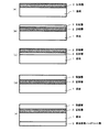
図2の概略断面図は、本発明における光記録媒体の層構成例(a)〜(e)を示す。
図2において、(a)は基板1と記録層2のみからなる層構成、(b)は基板1、記録層2、反射層3の順に積層した層構成、(c)は基板1、反射層3、記録層2の順に積層した層構成、(d)は基板1、記録層2、保護層4の順に積層した層構成、(e)は基板表面ハードコート層5、基板1、記録層2、保護層4の順に積層した層構成を示す。
<Configuration of optical recording medium>
The schematic cross-sectional view of FIG. 2 shows layer configuration examples (a) to (e) of the optical recording medium in the present invention.
In FIG. 2, (a) is a layer structure composed of only the substrate 1 and the recording layer 2, (b) is a layer structure in which the substrate 1, the recording layer 2, and the reflective layer 3 are laminated in this order, and (c) is the substrate 1 and the reflective layer. 3, a layer configuration in which the recording layer 2 is stacked in this order, (d) is a layer configuration in which the substrate 1, the recording layer 2, and the protective layer 4 are stacked in this order, and (e) is a substrate surface hard coat layer 5, substrate 1, and recording layer 2. The layer structure laminated | stacked in order of the protective layer 4 is shown.
本発明の光記録媒体の構成としては、通常の追記型光ディスクの構造(基板上に記録層を設けたものと他の基板を貼り合わせたいわゆるエアーサンドイッチ構造、または密着貼合わせ構造)としてもよく、CD−R用メディアの構造(基板上に記録層、反射層、保護層を設けた構造)としてもよく、CD−R構造を貼り合わせたDVD構造でもよい。なお、上記構成は実施の形態を説明するための例であって他の構成でもよい。以下に光記録媒体の各構成層について説明する。 The configuration of the optical recording medium of the present invention may be a normal write-once optical disc structure (a so-called air sandwich structure in which a recording layer is provided on a substrate and another substrate are bonded together, or a close bonding structure). A CD-R medium structure (a structure in which a recording layer, a reflective layer, and a protective layer are provided on a substrate) or a DVD structure in which a CD-R structure is bonded may be used. The above configuration is an example for describing the embodiment, and other configurations may be used. Hereinafter, each constituent layer of the optical recording medium will be described.
<基板>
光記録媒体の基板の必要特性としては、基板側より記録・再生を行う場合のみ使用レーザー光に対して透明でなければならず、基板と反対の記録層側から記録・再生を行う場合基板は透明である必要はない。
また、記録層とする有機博膜は、前述のように格子状パターンの孔内に機能性材料が吸着される必要があるので、基板も親水性であることが好ましい。必要により、基板に紫外線やプラズマを照射しての表面処理を施し、親水性として用いてもよい。
<Board>
As a necessary characteristic of the substrate of the optical recording medium, it must be transparent to the laser beam used only when recording / reproducing from the substrate side, and when recording / reproducing from the recording layer side opposite to the substrate, the substrate is It does not have to be transparent.
Further, since the organic film as the recording layer needs to have the functional material adsorbed in the holes of the lattice pattern as described above, the substrate is also preferably hydrophilic. If necessary, the substrate may be subjected to a surface treatment by irradiating with ultraviolet rays or plasma, and may be used as a hydrophilic property.
基板材料としては、例えば、ポリエステル、アクリル樹脂、ポリアミド、ポリカーボネート、ポリオレフィン、フェノール樹脂、エポキシ樹脂、ポリイミド等のプラスチック、石英、ガラス、セラミック、シリコンウェハー、あるいは金属等を用いることができる。なお、基板を1層しか用いない場合、あるいは基板2枚をサンドイッチ状で用いる場合は、基板表面にトラッキング用の案内溝や案内ピット、さらにアドレス信号等のプレフォーマットが形成されていてもよい。 As the substrate material, for example, plastic such as polyester, acrylic resin, polyamide, polycarbonate, polyolefin, phenol resin, epoxy resin, polyimide, quartz, glass, ceramic, silicon wafer, or metal can be used. When only one substrate is used, or when two substrates are used in a sandwich shape, tracking grooves and guide pits for tracking and a preformat such as an address signal may be formed on the substrate surface.
<記録層>
記録層は、本発明の有機薄膜から構成されるが、その格子状パターンの孔内に機能性部位として埋設された機能性材料は、レーザー光の照射によりなんらかの光学的変化を生じ、その光学的変化により情報の記録・再生が可能なものである。光学的変化としては、記録・再生用のレーザー波長に対する吸収特性変化あるいは屈折率変化が利用できる。
このような機能性材料としては、特に機能性色素が好ましく用いられる。なお、機能性部位として埋設された機能性色素のピットサイズ、すなわちドット径は、0.05〜5μmが適当である。
<Recording layer>
The recording layer is composed of the organic thin film of the present invention, but the functional material embedded as a functional part in the holes of the lattice pattern causes some optical change upon irradiation with laser light, and the optical layer Information can be recorded / reproduced by changes. As the optical change, a change in absorption characteristic or a change in refractive index with respect to the recording / reproducing laser wavelength can be used.
As such a functional material, a functional dye is particularly preferably used. In addition, 0.05-5 micrometers is suitable for the pit size of the functional pigment | dye embed | buried as a functional site | part, ie, a dot diameter.
機能性色素としては、例えば、レーザー光の照射エネルギーにより、熱分解等のヒートモードでその光学定数が変化する、ポリメチン色素、ナフタロシアニン系、フタロシアニン系、スクアリリウム系、クロコニウム系、ピリリウム系、ナフトキノン系、アントラキノン(インダンスレン)系、キサンテン系、トリフェニルメタン系、アズレン系、テトラヒドロコリン系、フェナンスレン系、トリフェノチアジン系の各染料、および金属キレート化合物等が挙げられ、これら色素を単独で用いてもよいし、2種以上の組合せで用いてもよい。 Examples of functional dyes include polymethine dyes, naphthalocyanine-based, phthalocyanine-based, squarylium-based, croconium-based, pyrylium-based, and naphthoquinone-based dyes whose optical constants change in a heat mode such as thermal decomposition depending on the irradiation energy of laser light. , Anthraquinone (indanthrene) series, xanthene series, triphenylmethane series, azulene series, tetrahydrocholine series, phenanthrene series, triphenothiazine series dyes, metal chelate compounds, and the like. It may also be used in combination of two or more.
また、レーザー光の照射エネルギーにより、フォトンモードでその光学定数が変化する、フルギド類、ジアリールエテン類、アゾベンゼン類、スピロピラン類、スチルベン類、ジヒドロピレン類、チオインジゴ類、ビピリジン類、アジリジン類、芳香族多環類、アリチリデンアニリン類、キサンテン類等のフォトクロミック材料も例として挙げられる。これらのフォトクロミック材料は、記録層における記録の書換えが可能であるため、特に好ましく用いられる。 In addition, the optical constant of the photon mode changes depending on the irradiation energy of the laser beam. Photochromic materials such as rings, allylidene anilines and xanthenes are also exemplified. These photochromic materials are particularly preferably used because the recording can be rewritten in the recording layer.
さらに、上記機能性色素と共に、安定剤(遷移金属錯体等)、紫外線吸収剤、分散剤、難燃剤、潤滑剤、帯電防止剤、界面活性剤、可塑剤などを添加して特性の改良を行ってもよい。 In addition to the above functional dyes, stabilizers (transition metal complexes, etc.), UV absorbers, dispersants, flame retardants, lubricants, antistatic agents, surfactants, plasticizers, etc. are added to improve the properties. May be.
機能性色素の光学特性としては、記録・再生用レーザー波長に対しその吸収特性変化を利用して記録・再生する場合にはレーザー波長近傍に最大吸収波長を持つことが好ましく、また、記録再生用レーザー波長に対しその屈折率変化を利用して記録・再生する場合にはレーザー波長近傍に最大屈折率を持つことが好ましい。
上記のように、レーザ光の発振波長近傍に最大吸収波長または最大屈折率を持つ機能性色素を用いることによって、記録層の光学特性変化を検知して光記録媒体の記録・再生を行う場合に、最もコントラストが得られる条件に合致させることができる。
As the optical characteristics of functional dyes, it is preferable to have a maximum absorption wavelength near the laser wavelength when recording / reproducing using the change in absorption characteristic with respect to the recording / reproducing laser wavelength. In the case of recording / reproducing using the change in the refractive index with respect to the laser wavelength, it is preferable to have the maximum refractive index in the vicinity of the laser wavelength.
As described above, when a functional dye having a maximum absorption wavelength or a maximum refractive index is used in the vicinity of the oscillation wavelength of the laser beam, when recording / reproduction of an optical recording medium is performed by detecting a change in the optical characteristics of the recording layer. , It is possible to meet the conditions for obtaining the most contrast.
<下引き層>
下引き層は、(a)接着性の向上、(b)水またはガス等のバリアー、(c)記録層の保存安定性の向上、(d)反射率の向上、(e)溶剤からの基板や記録層の保護、(f)案内溝、案内ピット、プレフォーマットの形成、等を目的として設けられる。
<Underlayer>
The undercoat layer comprises (a) improved adhesion, (b) a barrier such as water or gas, (c) improved storage stability of the recording layer, (d) improved reflectance, and (e) a substrate from a solvent. And (f) formation of guide grooves, guide pits, preformats, and the like.
(a)の目的に対しては、高分子材料、例えば、アイオノマー樹脂、ポリアミド、ビニル系樹脂、天然樹脂、天然高分子、シリコーン、液状ゴム等の種々の高分子物質や、シランカップリング剤等を用いることができる。また、(b)および(c)の目的に対しては、前記高分子材料以外に無機化合物、例えば、SiO2、MgF2、SiO、TiO2、ZnO、TiN、SiN等の金属、あるいは半金属、例えば、Zn、Cu、Ni、Cr、Ge、Se、Au、Ag、Al等を用いることができる。また、(d)の目的に対しては、金属、例えば、Al、Ag等や、金属光沢を有する有機薄膜、例えば、メチン染料、キサンテン系染料等を用いることができ、(e)および(f)の目的に対しては、紫外線硬化樹脂、熱硬化樹脂、熱可塑性樹脂等を用いることができる。下引き層の膜厚は、0.01〜30μm、好ましくは0.05〜10μmが適当である。 For the purpose of (a), polymer materials such as ionomer resins, polyamides, vinyl resins, natural resins, natural polymers, silicones, liquid rubbers, various polymer substances, silane coupling agents, etc. Can be used. For the purposes of (b) and (c), in addition to the polymer material, an inorganic compound, for example, a metal such as SiO 2 , MgF 2 , SiO, TiO 2 , ZnO, TiN, SiN, or a semimetal For example, Zn, Cu, Ni, Cr, Ge, Se, Au, Ag, Al, or the like can be used. For the purpose of (d), metals such as Al and Ag, and organic thin films having metallic luster such as methine dyes and xanthene dyes can be used, and (e) and (f ), An ultraviolet curable resin, a thermosetting resin, a thermoplastic resin, or the like can be used. The thickness of the undercoat layer is 0.01 to 30 μm, preferably 0.05 to 10 μm.
<反射層>
反射層としては、単体で高反射率が得られる腐食されにくい金属や、半金属等が用いられる。このような材料例としては、Au、Ag、Cr、Ni、Al、Fe、Sn、Cu等が挙げられるが、反射率、生産性の点からAu、Ag、Al、Cuが最も好ましく、これらの金属、半金属は単独で使用してもよく、2種以上の合金として用いてもよい。
反射層の膜形成法としては、蒸着、スッパタリング等が挙げられ、膜厚としては50〜5000Å、好ましくは100〜3000Åである。
<Reflective layer>
As the reflective layer, a metal that is highly corrosive and is not easily corroded, a semi-metal, or the like is used. Examples of such materials include Au, Ag, Cr, Ni, Al, Fe, Sn, Cu, etc., but Au, Ag, Al, Cu are most preferable from the viewpoint of reflectance and productivity. Metals and metalloids may be used alone or as two or more alloys.
Examples of the method for forming the reflective layer include vapor deposition and sputtering, and the film thickness is 50 to 5000 mm, preferably 100 to 3000 mm.
<保護層、基板表面ハードコート層>
保護層、または基板面ハードコート層としては、(a)記録層及び反射層を傷、ホコリ、汚れ等から保護する、(b)記録層及び反射層の保存安定性の向上、(c)反射率の向上等を目的として使用される。これらの目的に対しては、前記下引き層に示した材料を用いることができる。例えば、無機材料としてSiO、SiO2等を用いることができ、有機材料としてポリメチルアクリレート、ポリカーボネート、エポキシ樹脂、ポリスチレン、ポリエステル、ビニル樹脂、セルロース、脂肪族炭化水素樹脂、芳香属炭化水素樹脂、天然ゴム、スチレンブタジエン樹脂、クロロプレンゴム、ワックス、アルキッド樹脂、乾性油、ロジン等の熱軟化性、熱溶融性樹脂を用いることができる。
<Protective layer, substrate surface hard coat layer>
As the protective layer or the substrate hard coat layer, (a) the recording layer and the reflective layer are protected from scratches, dust, dirt, etc., (b) the storage stability of the recording layer and the reflective layer is improved, and (c) the reflection. It is used for the purpose of improving the rate. For these purposes, the materials shown in the undercoat layer can be used. For example, SiO, SiO 2 or the like can be used as the inorganic material, and polymethyl acrylate, polycarbonate, epoxy resin, polystyrene, polyester, vinyl resin, cellulose, aliphatic hydrocarbon resin, aromatic hydrocarbon resin, natural material as the organic material. Thermosoftening and heat melting resins such as rubber, styrene butadiene resin, chloroprene rubber, wax, alkyd resin, drying oil, and rosin can be used.
上記材料のうち保護層、または基板表面ハードコート層として最も好ましい例としては、生産性に優れた紫外線硬化樹脂である。保護層、または基板面ハードコート層の膜厚は、0.01〜30μm、好ましくは0.05〜10μmが適当である。本発明において、前記下引き層、保護層、および基板面ハードコート層には記録層の場合と同様に、安定剤、分散剤、難燃剤、滑剤、帯電防止剤、界面活性剤、可塑剤等を含有させることができる。 Of the above materials, the most preferable example of the protective layer or the substrate surface hard coat layer is an ultraviolet curable resin excellent in productivity. The film thickness of the protective layer or the substrate hard coat layer is 0.01 to 30 μm, preferably 0.05 to 10 μm. In the present invention, the undercoat layer, protective layer, and substrate surface hard coat layer are the same as in the recording layer, such as stabilizers, dispersants, flame retardants, lubricants, antistatic agents, surfactants, plasticizers, etc. Can be contained.
本発明の光記録媒体によれば、高度に秩序化されて構成された機能性部位、すなわち機能性色素からなる非連続な記録層ドットが最小記録ピットとして均一に形成される。従って、最小記録ピットのサイズは、レーザーの発振波長やレンズのNAによって決定されることなく、形成する記録層ドットのみで決まる。このため、任意の記録密度の記録媒体が設計可能となる。これによって、照射されるレーザ光の発振波長やレンズのNAに依存することなく、ピックアップレンズの回折限界を超えた記録密度の記録・再生が可能となる。また、このような構成の光記録媒体は、エラー発生が少なく低エラー率で、記録・再生信号が優れている。
さらに、記録ピットの最外周エッジもこの有機薄膜の記録層ドット全体を変化させるように記録することで、従来のレーザビームのガウス分布などの要因に基づく記録ピットの最外周エッジの不明瞭さなどの問題も回避され、記録ピットのバラツキの無い高品質の信号特性を得ることが可能となるため、このような構成の光記録媒体は、エラー発生が少なく低エラー率で、記録・再生信号が優れている。
According to the optical recording medium of the present invention, highly ordered functional parts, that is, non-continuous recording layer dots made of a functional dye are uniformly formed as minimum recording pits. Therefore, the size of the minimum recording pit is not determined by the laser oscillation wavelength or the lens NA, but only by the recording layer dots to be formed. Therefore, a recording medium having an arbitrary recording density can be designed. As a result, recording / reproduction with a recording density exceeding the diffraction limit of the pickup lens can be performed without depending on the oscillation wavelength of the irradiated laser beam or the NA of the lens. In addition, the optical recording medium having such a configuration has a low error rate with few errors and an excellent recording / reproducing signal.
Furthermore, by recording the outermost peripheral edge of the recording pit so that the entire recording layer dot of the organic thin film is changed, the ambiguity of the outermost peripheral edge of the recording pit based on factors such as the Gaussian distribution of the conventional laser beam, etc. Therefore, it is possible to obtain high-quality signal characteristics without variations in the recording pits. Therefore, the optical recording medium having such a configuration has a low error rate with a low error rate and a recording / reproduction signal. Are better.
また、本発明の光記録媒体の記録・再生方法は、基板上に設けられた記録層を形成する有機薄膜の格子状パターンの孔を最小単位とし、当該パターンの孔に埋設された機能性材料の光学特性をレーザ光の照射により変化させて行うものである。光学特性の変化としては、前記のように記録・再生用レーザー波長に対する吸収特性変化、あるいは屈折率変化等が利用される。 Further, the recording / reproducing method of the optical recording medium of the present invention is a functional material embedded in the holes of the pattern, with the holes of the lattice pattern of the organic thin film forming the recording layer provided on the substrate as a minimum unit. The optical characteristics are changed by irradiating with laser light. As the change in the optical characteristics, the change in the absorption characteristics with respect to the recording / reproducing laser wavelength or the change in the refractive index is used as described above.
本発明の光記録媒体の記録・再生方法によれば、レーザーの発振波長とレンズのNAで決定されるレーザービームの径に依存せず、光学系の実用化技術レベルに左右されない。
また、ビーム形状がガウス分布した形状であっても、前記のように記録層ドット全体を変化させるように記録することで、従来問題であったピットの最外周の大きさや変化量の問題も解決されて均一となる。
従って、ピックアップレンズの回折限界を超える記録密度で記録・再生が可能となり、その再生信号品質にもバラツキがなく、高品質の信号特性を得ることが可能となる。
According to the recording / reproducing method of the optical recording medium of the present invention, it does not depend on the laser beam diameter determined by the oscillation wavelength of the laser and the NA of the lens, and does not depend on the practical level of the optical system.
In addition, even if the beam shape is a Gaussian distribution, recording the entire recording layer dot as described above solves the problem of the size of the outermost periphery of the pit and the amount of change, which was a problem in the past. To be uniform.
Accordingly, recording / reproduction can be performed at a recording density exceeding the diffraction limit of the pickup lens, and the quality of the reproduced signal is not varied, and high-quality signal characteristics can be obtained.
以下、実施例を挙げて本発明をさらに具体的に説明するが、本発明はその趣旨を逸脱しない限り下記実施例に限定されるものではない。 Hereinafter, the present invention will be described more specifically with reference to examples. However, the present invention is not limited to the following examples without departing from the gist thereof.
実施例1
数平均分子量が凡そ60,000のポリスチレン(PSt)ブロック重合体と、ポリ側鎖型オリゴチオフェン(POTI)ブロック重合体との共重合体からなるポリマーを合成した。なお、共重合体中に占めるPStの割合(体積比)は92vol%である。
Example 1
A polymer composed of a copolymer of a polystyrene (PSt) block polymer having a number average molecular weight of approximately 60,000 and a poly side chain type oligothiophene (POTI) block polymer was synthesized. In addition, the ratio (volume ratio) of PSt which occupies in a copolymer is 92 vol%.
次に、合成したポリマーを二硫化炭素に、濃度3.0g/lで溶解して疎水性有機溶媒溶液を調製した。この疎水性有機溶媒溶液をマイカ基板上にキャストした後、室温で、相対湿度80%の状態で静置し、薄膜を形成した。 Next, the synthesized polymer was dissolved in carbon disulfide at a concentration of 3.0 g / l to prepare a hydrophobic organic solvent solution. After casting this hydrophobic organic solvent solution on a mica substrate, it was allowed to stand at room temperature and a relative humidity of 80% to form a thin film.
次いで、形成された薄膜の上から3,3,3’,3’−テトラメチル−1,1’−ビス(3−スルフォエチル)−2,2’−インドジカルボシアニンヒドロキシドトリエチルアミン塩の1wt%水溶液をキャストした後、乾燥して有機薄膜を形成した。 Next, 1 wt% of 3,3,3 ′, 3′-tetramethyl-1,1′-bis (3-sulfoethyl) -2,2′-indodicarbocyanine hydroxide triethylamine salt is formed on the formed thin film. After casting the aqueous solution, it was dried to form an organic thin film.
上記により得られた有機薄膜を光学顕微鏡、原子間力顕微鏡、およびレーザ゛顕微鏡等を用いて観察した。その結果、二次元方向に規則的な格子状のパターン(約1.5μmの格子)からなるポリマー構造体、いわゆるポリマーネットワークが、秩序良く均一に形成されており、その格子状のパターンの孔内に色素がサブミクロンサイズでパッキングされた状態で入り込んでいる様子が観察された。 The organic thin film obtained as described above was observed using an optical microscope, an atomic force microscope, a laser microscope, and the like. As a result, a polymer structure consisting of a regular lattice pattern (about 1.5 μm lattice) in a two-dimensional direction, a so-called polymer network, is formed in an orderly and uniform manner. It was observed that the pigment entered the submicron size in a packed state.
実施例2
実施例1と同じ条件でポリスチレン(PSt)ブロック重合体と、ポリ側鎖型オリゴチオフェン(POTI)ブロック重合体との共重合体からなるポリマーを合成し、得られたポリマーを二硫化炭素に溶解して疎水性有機溶媒溶液を調製した。実施例1と同様に、この疎水性有機溶媒溶液をマイカ基板上にキャストし、薄膜を形成した。
Example 2
A polymer composed of a copolymer of a polystyrene (PSt) block polymer and a poly side chain type oligothiophene (POTI) block polymer was synthesized under the same conditions as in Example 1, and the resulting polymer was dissolved in carbon disulfide. Thus, a hydrophobic organic solvent solution was prepared. As in Example 1, this hydrophobic organic solvent solution was cast on a mica substrate to form a thin film.
次いで、形成された薄膜の上からスルホン酸基を有するスピロピラン化合物の水溶液をキャストした後、乾燥して有機薄膜を形成した。 Next, an aqueous solution of a spiropyran compound having a sulfonic acid group was cast from above the formed thin film, and then dried to form an organic thin film.
上記により得られた有機薄膜を実施例1と同じように観察した。その結果、二次元方向に規則的な格子状のパターン(約1.5μmの格子)からなるポリマーネットワークが、秩序良く均一に形成されており、その格子状のパターンの孔内に色素がサブミクロンサイズでパッキングされた状態で入り込んでいる様子が観察された。 The organic thin film obtained as described above was observed in the same manner as in Example 1. As a result, a polymer network consisting of a regular lattice pattern (about 1.5 μm lattice) in a two-dimensional direction is formed in an orderly and uniform manner, and the dye is submicron in the pores of the lattice pattern. It was observed that it was packed in size.
実施例3
数平均分子量が凡そ56,000のポリスチレン(PSt)ブロック重合体と、ポリフェニルキノリン(PPQ)ブロック重合体との共重合体からなるポリマーを合成した。なお、共重合体中に占めるPStの割合(体積比)は90vol%である。
Example 3
A polymer composed of a copolymer of a polystyrene (PSt) block polymer having a number average molecular weight of approximately 56,000 and a polyphenylquinoline (PPQ) block polymer was synthesized. In addition, the ratio (volume ratio) of PSt which occupies in a copolymer is 90 vol%.
次に、合成したポリマーを二硫化炭素に、濃度1.5g/lで溶解して疎水性有機溶媒溶液を調製した。この疎水性有機溶媒溶液をマイカ基板上にキャストした後、室温で、相対湿度65%の状態で静置し、薄膜を形成した。
次いで、マイカ基板ごとスルホン酸基を有するスピロピラン化合物の水溶液に常圧で、浸漬した後、乾燥して有機薄膜を形成した。
Next, the synthesized polymer was dissolved in carbon disulfide at a concentration of 1.5 g / l to prepare a hydrophobic organic solvent solution. After casting this hydrophobic organic solvent solution on a mica substrate, it was allowed to stand at a room temperature and a relative humidity of 65% to form a thin film.
Next, the mica substrate was immersed in an aqueous solution of a spiropyran compound having a sulfonic acid group at normal pressure, and then dried to form an organic thin film.
上記により得られた有機薄膜を実施例1と同じように観察した。その結果、二次元方向に規則的な格子状のパターン(約2.1μmの格子)からなるポリマーネットワークが、秩序良く均一に形成されており、その格子状のパターンの孔内に色素がサブミクロンサイズでパッキングされた状態で入り込んでいる様子が観察された。 The organic thin film obtained as described above was observed in the same manner as in Example 1. As a result, a polymer network consisting of a regular lattice pattern (about 2.1 μm lattice) in a two-dimensional direction is formed in an orderly and uniform manner, and the dye is submicron in the pores of the lattice pattern. It was observed that it was packed in size.
実施例4
数平均分子量が凡そ50,000のポリスチレン(PSt)ブロック重合体と、ポリパラフェニレン(PPP)ブロック重合体との共重合体からなるポリマーを合成した。なお、共重合体中に占めるPStの割合(体積比)は93vol%である。
Example 4
A polymer comprising a copolymer of a polystyrene (PSt) block polymer having a number average molecular weight of about 50,000 and a polyparaphenylene (PPP) block polymer was synthesized. In addition, the ratio (volume ratio) of PSt which occupies in a copolymer is 93 vol%.
次に、合成したポリマーを二硫化炭素に、濃度1.5g/lで溶解して疎水性有機溶媒溶液を調製した。この疎水性有機溶媒溶液をマイカ基板上にキャストした後、室温で、相対湿度65%の状態で静置し、薄膜を形成した。 Next, the synthesized polymer was dissolved in carbon disulfide at a concentration of 1.5 g / l to prepare a hydrophobic organic solvent solution. After casting this hydrophobic organic solvent solution on a mica substrate, it was allowed to stand at a room temperature and a relative humidity of 65% to form a thin film.
次いで、マイカ基板ごとトリス(p−ジメチルアミノフェニル)メチリウムヘキサフルオロアンチモン塩の0.5wt%メタノール/ピリジン(20/1:重量比)溶液の中に常圧で、浸漬した後、乾燥して有機薄膜を形成した。 Next, the mica substrate is immersed in a 0.5 wt% methanol / pyridine (20/1: weight ratio) solution of tris (p-dimethylaminophenyl) methylium hexafluoroantimony salt at normal pressure and then dried. An organic thin film was formed.
上記により得られた有機薄膜を実施例1と同じように観察した。その結果、二次元方向に規則的な格子状のパターン(約2.6μmの格子)からなるポリマーネットワークが、秩序良く均一に形成されており、その格子状のパターンの孔内に色素がサブミクロンサイズでパッキングされた状態で入り込んでいる様子が観察された。 The organic thin film obtained as described above was observed in the same manner as in Example 1. As a result, a polymer network composed of a regular lattice pattern (approximately 2.6 μm lattice) in a two-dimensional direction is formed in an orderly and uniform manner, and the dye is submicron in the pores of the lattice pattern. It was observed that it was packed in size.
以上の結果から、本発明における共重合体を用いて形成した有機薄膜は、パターンやサイズの均一性が良好な格子状構造の孔内にナノメートルサイズで秩序だった機能性部位を有する構造であることが分った。このような新規な構造を持つ有機薄膜を用いることにより、新たな電子的性質、導電的性質、光学的性質、磁気的性質等の発現が期待される。 From the above results, the organic thin film formed by using the copolymer in the present invention has a structure having functional parts ordered in nanometer size in the pores of a lattice structure having good pattern and size uniformity. I found that there was. By using an organic thin film having such a novel structure, it is expected that new electronic properties, conductive properties, optical properties, magnetic properties, and the like are exhibited.
実施例5
実施例1において用いた基板を石英基板に代えた以外はまったく同様にして、光記録媒体を作製した。
作製した光記録媒体を用いて、その記録層に、発振波長405nm、ビーム径0.6μmの半導体レーザーを、水平方向に5mmスキャンさせた。このときの照射部および未照射部について、走査型電子顕微鏡、光学顕微鏡による観察、顕微分光法による透過率および反射率の測定を行った。評価結果を下記表1に示す。
Example 5
An optical recording medium was produced in exactly the same manner except that the substrate used in Example 1 was replaced with a quartz substrate.
Using the produced optical recording medium, a semiconductor laser having an oscillation wavelength of 405 nm and a beam diameter of 0.6 μm was scanned 5 mm horizontally in the recording layer. The irradiated part and the unirradiated part at this time were observed with a scanning electron microscope and an optical microscope, and the transmittance and reflectance were measured by a microspectroscopic method. The evaluation results are shown in Table 1 below.
実施例6
実施例3において用いた基板を石英基板に代えた以外はまったく同様にして、光記録媒体を作製した。
作製した光記録媒体を用いて、その記録層に、発振波長405nm、ビーム径0.6μmの半導体レーザーを、水平方向に5mmスキャンさせた。このときの照射部および未照射部について、走査型電子顕微鏡、光学顕微鏡による観察、顕微分光法による透過率および反射率の測定を行った。評価結果を下記表1に示す。
Example 6
An optical recording medium was produced in exactly the same manner except that the substrate used in Example 3 was replaced with a quartz substrate.
Using the produced optical recording medium, a semiconductor laser having an oscillation wavelength of 405 nm and a beam diameter of 0.6 μm was scanned 5 mm horizontally in the recording layer. The irradiated part and the unirradiated part at this time were observed with a scanning electron microscope and an optical microscope, and the transmittance and reflectance were measured by a microspectroscopic method. The evaluation results are shown in Table 1 below.
比較例1
実施例5と同じポリマー(実施例1と同じ)を用いて、同様に石英基板上に薄膜を形成した状態、すなわち機能性色素水溶液をキャストせず、ポリマーネットワークが形成された状態のままで、実施例5と同様にレーザーでスキャンし、照射部および未照射部について、走査型電子顕微鏡、光学顕微鏡による観察、顕微分光法による透過率および反射率の測定を行った。評価結果を下記表1に示す。
Comparative Example 1
Using the same polymer as in Example 5 (same as Example 1), similarly, a thin film was formed on a quartz substrate, that is, the functional dye aqueous solution was not cast, and the polymer network was formed. In the same manner as in Example 5, scanning with a laser was performed, and the irradiated part and the unirradiated part were observed with a scanning electron microscope and an optical microscope, and the transmittance and reflectance were measured with a microspectrophotometry. The evaluation results are shown in Table 1 below.
比較例2
実施例6と同じポリマー(実施例3と同じ)を用いて、同様に石英基板上に薄膜を形成した状態、すなわち機能性色素水溶液に浸漬せず、ポリマーネットワークが形成された状態のままで、実施例6と同様にレーザーでスキャンし、照射部および未照射部について、走査型電子顕微鏡、光学顕微鏡による観察、顕微分光法による透過率および反射率の測定を行った。評価結果を下記表1に示す。
Comparative Example 2
Using the same polymer as in Example 6 (same as in Example 3), similarly, a thin film was formed on a quartz substrate, that is, not immersed in a functional dye aqueous solution, and a polymer network was formed. In the same manner as in Example 6, scanning with a laser was performed, and the irradiated part and the unirradiated part were observed with a scanning electron microscope and an optical microscope, and the transmittance and reflectance were measured with a microspectroscopic method. The evaluation results are shown in Table 1 below.

上記観察および測定から、本発明に基づいて作製された有機薄膜は、レーザー光の照射によって光学特性が変化し、サブミクロンサイズの機能性部位に記録が可能であることが確認された。 From the above observations and measurements, it was confirmed that the organic thin film produced according to the present invention changed its optical properties by irradiation with laser light and could be recorded on a functional region of submicron size.
1 基板
2 記録層
3 反射層
4 保護層
5 基板表面ハードコート層
DESCRIPTION OF SYMBOLS 1 Substrate 2 Recording layer 3 Reflective layer 4 Protective layer 5 Substrate surface hard coat layer
Claims (14)
前記ポリマーが、疎水性有機溶媒に可溶なブロック重合体と難溶なブロック重合体との共重合体からなり、該疎水性有機溶媒に可溶なブロック重合体がポリスチレンであり、かつ該ポリスチレンの共重合体に占める割合(体積比)が90vol%以上であることを特徴とする有機薄膜。 In an organic thin film composed of a polymer structure having a regular lattice pattern in a two-dimensional direction and a functional material embedded in the holes of the lattice pattern,
The polymer comprises a copolymer of a block polymer soluble in a hydrophobic organic solvent and a block polymer hardly soluble, and the block polymer soluble in the hydrophobic organic solvent is polystyrene, and the polystyrene The organic thin film characterized by the ratio (volume ratio) which occupies for the copolymer of 90 vol% or more.
前記有機薄膜は、二次元方向に規則的な格子状のパターンを有するポリマー構造体と、該格子状パターンの孔内に埋設された機能性材料とから構成されるとともに、前記ポリマーが、疎水性有機溶媒に可溶なブロック重合体と難溶なブロック重合体との共重合体からなり、該疎水性有機溶媒に可溶なブロック重合体がポリスチレンで、かつ該ポリスチレンの共重合体に占める割合(体積比)が90vol%以上であることを特徴とする光記録媒体。 In an optical recording medium provided with a recording layer made of an organic thin film on a substrate,
The organic thin film is composed of a polymer structure having a regular lattice pattern in a two-dimensional direction and a functional material embedded in the holes of the lattice pattern, and the polymer is hydrophobic It consists of a copolymer of a block polymer soluble in an organic solvent and a hardly soluble block polymer, and the block polymer soluble in the hydrophobic organic solvent is polystyrene and the proportion of the polystyrene in the copolymer An optical recording medium having a (volume ratio) of 90 vol% or more.
前記記録・再生が、有機薄膜に形成された格子状のパターンの孔を最小単位とし、照射光により孔内に埋設された機能性材料の光学特性を変化させて行われるようにしたことを特徴とする光記録媒体の記録・再生方法。
In the recording / reproducing method of the optical recording medium which records and reproduces by irradiating a laser beam to the optical recording medium in any one of Claims 9-13,
The recording / reproducing is performed by changing the optical characteristic of the functional material embedded in the hole by irradiation light with the minimum unit being a lattice-shaped pattern hole formed in the organic thin film. Recording / reproducing method of optical recording medium.
Priority Applications (1)
| Application Number | Priority Date | Filing Date | Title |
|---|---|---|---|
| JP2004184759A JP4331060B2 (en) | 2004-06-23 | 2004-06-23 | Organic thin film and manufacturing method thereof, optical recording medium using the thin film, and recording / reproducing method |
Applications Claiming Priority (1)
| Application Number | Priority Date | Filing Date | Title |
|---|---|---|---|
| JP2004184759A JP4331060B2 (en) | 2004-06-23 | 2004-06-23 | Organic thin film and manufacturing method thereof, optical recording medium using the thin film, and recording / reproducing method |
Publications (2)
| Publication Number | Publication Date |
|---|---|
| JP2006012232A JP2006012232A (en) | 2006-01-12 |
| JP4331060B2 true JP4331060B2 (en) | 2009-09-16 |
Family
ID=35779315
Family Applications (1)
| Application Number | Title | Priority Date | Filing Date |
|---|---|---|---|
| JP2004184759A Expired - Fee Related JP4331060B2 (en) | 2004-06-23 | 2004-06-23 | Organic thin film and manufacturing method thereof, optical recording medium using the thin film, and recording / reproducing method |
Country Status (1)
| Country | Link |
|---|---|
| JP (1) | JP4331060B2 (en) |
Families Citing this family (1)
| Publication number | Priority date | Publication date | Assignee | Title |
|---|---|---|---|---|
| JP2007237407A (en) * | 2006-03-06 | 2007-09-20 | Meiki Co Ltd | Disk substrate molding method and blue lay disk |
-
2004
- 2004-06-23 JP JP2004184759A patent/JP4331060B2/en not_active Expired - Fee Related
Also Published As
| Publication number | Publication date |
|---|---|
| JP2006012232A (en) | 2006-01-12 |
Similar Documents
| Publication | Publication Date | Title |
|---|---|---|
| JP2007015221A (en) | Manufacturing method for organic membrane | |
| JP4331060B2 (en) | Organic thin film and manufacturing method thereof, optical recording medium using the thin film, and recording / reproducing method | |
| EP0836180B1 (en) | An optical recording medium with a metallic recording layer | |
| JP4117872B2 (en) | Organic thin film, method for producing the same, and optical recording medium using the same | |
| JP4157425B2 (en) | Organic functional thin film, manufacturing method thereof, and optical recording medium provided with organic functional thin film | |
| JP2006213939A (en) | Organic and inorganic compound thin film, method of manufacturing the same, and optical recording medium using the same | |
| JP4056783B2 (en) | Organic thin film manufacturing method and optical recording medium using the same | |
| JP4311907B2 (en) | Organic thin film, method for producing the same, and optical recording medium using the same | |
| JP4233970B2 (en) | Organic thin film, method for producing the same, and optical recording medium using the same | |
| JP4093831B2 (en) | Organic thin film, method for producing the same, and optical recording medium using the same | |
| JP4519684B2 (en) | ORGANIC THIN FILM, ITS MANUFACTURING METHOD, AND OPTICAL RECORDING MEDIUM USING THE ORGANIC THIN FILM | |
| JP4563220B2 (en) | Organic thin film and optical recording medium using the same | |
| JP2003089269A (en) | Organic thin film, method for manufacturing organic thin film, optical recording medium using the film, and method for regenerating records of optical recording medium | |
| JP2010049741A (en) | Nano structure and optical recording medium using the same | |
| JP2009064496A (en) | Organic thin film and optical recording medium using the same | |
| JP4523575B2 (en) | Structure and optical recording medium using the same | |
| JP2007242188A (en) | Structure and optical recording medium using the same | |
| JP2003094825A (en) | Organic film and its manufacturing method, optical recording medium using the same, and its recording/ reproducing method | |
| JP4044482B2 (en) | Optical recording medium and recording / reproducing method thereof | |
| JP2004050676A (en) | Functional organic thin film, its manufacturing method and optical recording medium using the same | |
| JP4758929B2 (en) | Structure having base material and organic thin film, and optical recording medium using the structure | |
| JP2007305271A (en) | Functional inorganic thin film, manufacturing method thereof, and optical recording medium | |
| JP4468233B2 (en) | Optical recording medium using block copolymer monomolecular film and method for producing the same | |
| JP3600177B2 (en) | Optical recording medium and manufacturing method thereof | |
| JP2006252613A (en) | Optical recording medium |
Legal Events
| Date | Code | Title | Description |
|---|---|---|---|
| A621 | Written request for application examination |
Free format text: JAPANESE INTERMEDIATE CODE: A621 Effective date: 20060926 |
|
| A977 | Report on retrieval |
Free format text: JAPANESE INTERMEDIATE CODE: A971007 Effective date: 20080422 |
|
| A131 | Notification of reasons for refusal |
Free format text: JAPANESE INTERMEDIATE CODE: A131 Effective date: 20080430 |
|
| TRDD | Decision of grant or rejection written | ||
| A01 | Written decision to grant a patent or to grant a registration (utility model) |
Free format text: JAPANESE INTERMEDIATE CODE: A01 Effective date: 20090616 |
|
| A01 | Written decision to grant a patent or to grant a registration (utility model) |
Free format text: JAPANESE INTERMEDIATE CODE: A01 |
|
| A61 | First payment of annual fees (during grant procedure) |
Free format text: JAPANESE INTERMEDIATE CODE: A61 Effective date: 20090617 |
|
| R150 | Certificate of patent or registration of utility model |
Free format text: JAPANESE INTERMEDIATE CODE: R150 |
|
| FPAY | Renewal fee payment (event date is renewal date of database) |
Free format text: PAYMENT UNTIL: 20120626 Year of fee payment: 3 |
|
| FPAY | Renewal fee payment (event date is renewal date of database) |
Free format text: PAYMENT UNTIL: 20130626 Year of fee payment: 4 |
|
| LAPS | Cancellation because of no payment of annual fees |