JP4323663B2 - Image filter circuit and image filtering method - Google Patents
Image filter circuit and image filtering method Download PDFInfo
- Publication number
- JP4323663B2 JP4323663B2 JP2000053736A JP2000053736A JP4323663B2 JP 4323663 B2 JP4323663 B2 JP 4323663B2 JP 2000053736 A JP2000053736 A JP 2000053736A JP 2000053736 A JP2000053736 A JP 2000053736A JP 4323663 B2 JP4323663 B2 JP 4323663B2
- Authority
- JP
- Japan
- Prior art keywords
- histogram
- pixel
- delay
- region
- filter circuit
- Prior art date
- Legal status (The legal status is an assumption and is not a legal conclusion. Google has not performed a legal analysis and makes no representation as to the accuracy of the status listed.)
- Expired - Fee Related
Links
- 238000000034 method Methods 0.000 title claims description 20
- 238000001914 filtration Methods 0.000 title claims description 7
- 230000001186 cumulative effect Effects 0.000 claims description 25
- 230000001174 ascending effect Effects 0.000 claims description 20
- 230000003111 delayed effect Effects 0.000 claims description 4
- 230000001934 delay Effects 0.000 claims description 2
- 238000009825 accumulation Methods 0.000 claims 1
- 239000011159 matrix material Substances 0.000 description 35
- 238000010586 diagram Methods 0.000 description 19
- 230000001360 synchronised effect Effects 0.000 description 2
- 230000000694 effects Effects 0.000 description 1
- 238000012986 modification Methods 0.000 description 1
- 230000004048 modification Effects 0.000 description 1
- 230000002093 peripheral effect Effects 0.000 description 1
Images


Classifications
-
- G06T5/70—
-
- G—PHYSICS
- G06—COMPUTING; CALCULATING OR COUNTING
- G06T—IMAGE DATA PROCESSING OR GENERATION, IN GENERAL
- G06T5/00—Image enhancement or restoration
- G06T5/40—Image enhancement or restoration by the use of histogram techniques
Landscapes
- Physics & Mathematics (AREA)
- General Physics & Mathematics (AREA)
- Engineering & Computer Science (AREA)
- Theoretical Computer Science (AREA)
- Image Processing (AREA)
- Picture Signal Circuits (AREA)
- Facsimile Image Signal Circuits (AREA)
Description
【0001】
【発明の属する技術分野】
本発明は画像フィルタ回路及び画像フィルタリング方法に関し、特にデジタル画像からスパイク状の雑音を除去する画像フィルタ回路及び画像フィルタリング方法に関する。
【0002】
【従来の技術】
画像におけるスパイク状の孤立点雑音を除去する非線形フィルタとして、メディアンフィルタが知られている。
【0003】
メディアンフィルタとは、原画像上の注目画素に対して、その周辺に任意のサイズのマトリクスを作成し、そのマトリクス内の画素値を大きい順にソーティングした際に丁度中央番目となる画素値を、注目画素の値とするフィルタである。
【0004】
以下、図2及び図3を参照して、一般的なメディアンフィルタについて詳細に説明する。
【0005】
図2に示すように、原画像上においてマトリクスを水平もしくは垂直方向に順次移動する事により、原画像上のすべての画素に対してフィルタ処理を施すことができる。
【0006】
図3は、メディアンフィルタを実現する回路構成を示す図である。即ち、メディアンフィルタを回路として実現するためには、ソーティング処理を行うための比較器として、コンパレータ回路とセレクタ回路をソーティング時の比較回数分用意し、これらを順次組み合わせてネットワークを構成すればよい。
【0007】
例えば、M×Mサイズ(Mは自然数)マトリクスに対するソーティング処理を、コンパレータ回路とスイッチ回路、及びデータラッチによって実現する技術が、ソーティング・アンド・サーチング,ザ・アート・オブ・コンピュータ・プログラミングに示されている。
【0008】
【発明が解決しようとする課題】
上記ソーティング・アンド・サーチング,ザ・アート・オブ・コンピュータ・プログラミングに示されているマージソート技術によれば、例えばM=3の場合には、25個のコンパレータとセレクタ回路、及び72個のデータラッチとによって、メディアンフィルタ回路が構成される。ただし、これをデジタル回路として構成するためにクロック同期型で実現しようとすると、更に90個のデータラッチと3個のロード付きデータラッチが必要となる。
【0009】
更に、M=4の場合についてメディアンフィルタ回路を構成すると、54個のコンパレータとセレクタ回路、及び176個のデータラッチと4個のロード付きデータラッチが必要となってしまう。
【0010】
このように、上記技術によって、メディアンフィルタをハードウエアとして実現すると、処理対象とするマトリクスサイズMの値が大きくなるに従い、回路規模が急激に増大してしまうという問題があった。
【0011】
例えば、上記技術を用いてM=7のマトリクスサイズによってメディアンフィルタ回路を構成する場合について考えると、データ間の同期を考慮すると、デジタル回路として実現するには回路規模があまりに大きいため、その実現は困難である。
【0012】
更に、特開平5−233802号によれば、比較回路によるソーティング処理を行わずに、画素値のテーブルを作成してメディアンフィルタを構成するという技術が示されている。しかしながら、その処理の具体的手法、及びハードウエアでの実現性に対しては何ら言及されておらず、現実的ではなかった。
【0013】
本発明は上記問題を解決するためになされたものであり、大規模メディアンフィルタをデジタル回路として実現可能な画像フィルタ回路及び画像フィルタリング方法を提供することを目的とする。
【0014】
【課題を解決するための手段】
上記目的を達成するための一手段として、本発明の画像フィルタ回路は以下の構成を備える。
【0015】
即ち、原画像における注目画素とその周辺画素を含む領域内の各画素の値を入力して、前記注目画素の値を前記領域内における所定の昇順番目の画素値で置き換えるフィルタを、所定方向に移動させて1フレームの画像データを得る画像フィルタ回路であって、前記領域内における画素の上位ビットデータによる第1のヒストグラムを作成する第1のヒストグラム作成手段と、前記第1のヒストグラムに基づいて、前記所定の昇順番目に相当する画素値を含む階級を目標階級として検索する第1の検索手段と、前記目標階級に含まれる画素の下位ビットデータによる第2のヒストグラムを作成する第2のヒストグラム作成手段と、前記第2のヒストグラムに基づいて、前記領域内における前記所定の昇順番目の画素値を検索する第2の検索手段と、を有することを特徴とする。
【0016】
【発明の実施の形態】
以下、本発明に係る一実施形態について、図面を参照して詳細に説明する。
【0017】
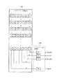
図1は、本実施形態におけるメディアンフィルタを実現するデジタル回路(以下、単にフィルタ回路と称する)のブロック構成を示す図である。尚、本実施形態におけるフィルタ回路は、クロック同期を可能とするデジタル回路構成をなす。
【0018】
以下、同図を参照して、マトリクスサイズM=5、原画像の画像データのビット精度L=8ビットの場合を例として説明する。
【0019】
原画像上において、5×5のマトリクスが水平方向に、クロック毎に1画素分移動したとする。この時、新たにマトリクスの構成要素となった列の画素が、遅延部101及びヒストグラムA更新部102に入力される。
【0020】
[遅延部101]
図4は、遅延部101の回路構成を示す図である。
【0021】
遅延部101は、2つのデータパス(遅延パスA201,遅延パスB202)から構成されている。これら遅延パスA201及び遅延パスB202は共に、図示される回路を並列に5つ備えており、列データがそれぞれ同一タイミングで入力される。
【0022】
一方の遅延パスA201は、画素データの上位5ビット(P=5)について、クロック毎に入力されるマトリクスの5つの列構成データDelayA0(0)〜DelayA0(4)を、フリップフロップ(以下、FFと表記)にて5クロック、即ち、マトリクスの水平サイズである5画素相当分を遅延させ、最終的にDelayA5(0)〜DelayA5(4)を出力する。尚、各FFからの1クロック毎の遅延出力をそれぞれ、DelayA1(0)〜DelayA1(4),DelayA2(0)〜DelayA2(4),DelayA3(0)〜DelayA3(4),DelayA4(0)〜DelayA4(4)として、DelayA5(0)〜DelayA5(4)と共に、後述する領域選択部105へ出力する。遅延パスA201は即ち、マトリクスの1行分を遅延しているに過ぎない。
【0023】
他方の遅延パスB202は、画素データの下位3ビット(L−P=3)について、列構成データの値を3To8デコーダを介して8ビット(2L−P=8)のFFに入力し、同様に5クロック遅延させる。そして、各FFからの1クロック毎の遅延出力をそれぞれ、DelayA1_Low(0)〜DelayA1_Low(4),DelayA2_Low(0)〜DelayA2_Low(4),DelayA3_Low(0)〜DelayA3_Low(4),DelayA4_Low(0)〜DelayA4_Low(4),DelayA5_Low(0)〜DelayA5_Low(4)として、後述する領域選択部105へ出力する。
【0024】
遅延パスA201及び遅延パスB202はそれぞれ、各FFによる遅延データによって、画像データの各列に対する上位5ビットデータ及び下位3ビットデータのヒストグラム(詳細は後述する)を生成している。
【0025】
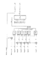
[ヒストグラムA更新部102]
図5は、ヒストグラムA更新部102及びヒストグラムA保持部103の回路構成を示す図である。
【0026】
ヒストグラムA保持部103は、画像データの各列に対する上位5ビットデータのヒストグラムAを保持するレジスタ群であり、マトリクス内の画素要素数25(M2)個を表現可能な、5ビット幅をもつFF群を32(2P)個並列に並べることによって構成されている。この32個のFFそれぞれが、ヒストグラムAにおける各階級に相当し、各階級の度数は即ち画素数である。
【0027】
ヒストグラムA保持部103の出力はヒストグラムA更新部102へ入力されて、各階級毎に5(マトリクス列サイズMに相当)段のインクリメント部501と、同じく5段のディクリメント部502を通すことによって、ヒストグラムAが更新される。即ち、マトリクスを移動する事によって新規マトリクス構成要素なる5個の画素データ(DelayA0(0)〜DelayA0(4))と、マトリクス外要素となる5個の画素データ(DelayA5(0)〜DelayA5(4))に基づいて、ヒストグラムAを更新する。
【0028】
インクリメント部501へは、遅延部101の遅延パスA201への入力と同様の列データDelayA0(0)〜DelayA0(4)が入力され、ディクリメント部502へは、遅延部101にてマトリクスの水平サイズ分遅延した列データDelayA5(0)〜DelayA5(4)が、それぞれ入力される。このインクリメンタとディクリメンタの組み合わせ回路がシリアルに5段接続され、ヒストグラムA保持部103における各FFに入力される。
【0029】
図6は、インクリメント部501の詳細構成を示す図である。以下、DelayA0(0)〜DelayA0(4)はマトリクスの列を構成する5画素を束ねたデータバスであるが、その中の一つであるDelayA0(0)がインクリメント部501に入力される場合について、以下説明する。
【0030】
セレクタ602によって、5ビットデータであるDelayA0(0)を32(25)ビットにデコードした各出力、即ちヒストグラムAの32階級値をそれぞれ、データ更新部601における32個のユニットに接続する。データ更新部601は、入力データに対してインクリメントを行うパスと、入力データ値に処理を加えずにそのまま出力するパスとを備えたユニットを32個備えており、各ユニットにおいては、DelayA0(0)の値に相当する階級についてはインクリメンタ出力のパスが選択され、それ以外の場合にはそのまま出力するパスが選択される。
【0031】
尚、デクリメント部502の構成は、図6に示したインクリメント部501の構成において、データ更新部601内のインクリメンタをデクリメンタに置き換えたものとなる。
【0032】
[累積加算部A104]
図7は、累積加算部A104の回路構成を示す図である。
【0033】
累積加算部A104においては、ヒストグラムA保持部103に保持されたヒストグラムAから、その中央値を含む階級(以下、目標階級と称する)を検索するために、階級毎の度数(画素数)を累積加算する。
【0034】
マトリクスサイズが5×5であるから、ヒストグラムAの中央値は昇順で13番目の画素値となる。従って、ヒストグラムA保持部103からの各5ビットのFF出力が階級毎に昇順で加算器に入力され、その各出力はコンパレータによって、それぞれ固定値「13」と比較される。このコンパレータ出力により、ヒストグラムにおいて階級毎の累積度数(累積画素数)が最初に13を超えた階級が目標階級であり、即ち中央値が含まれている階級であると判定することができる。
【0035】
全32個のコンパレータ出力は、中央値の上位5ビット(P=5)出力(図中、Median_Upper5)と、ヒストグラムにおける該中央値を含む階級までの合計画素数(図中、Median_Sum)の、選択信号として使用される。即ち、累積加算部A104から出力されるMedian_Upper5が目標階級を示し、Median_Sumが該目標階級までの合計画素数を示す。
【0036】
[領域選択部105]
図8は、領域選択部105の回路構成を示す図である。
【0037】
領域選択部105においては、ヒストグラムAの目標階級を構成する画素データのみを選択する。
【0038】
領域選択部105においては、累積加算部A104から入力されるMedian_Upper5信号と、遅延部101の遅延パスA201から入力された25個の上位5ビットの遅延データ(DelayA1(0〜5)〜DelayA5(0〜5))とをそれぞれ比較することによって、マトリクス要素である25個の画素からMedian_Upper5と同一値を有するものを選択する。
【0039】
領域選択部105には更に、遅延パスB202から出力された下位3ビットをデコードした8ビット信号(DelayA1_Low(0〜5)〜DelayA5_Low(0〜5))が、マトリクス内の全ての画素に対応する形で入力される。
【0040】
これにより領域選択部105からは、マトリクスを構成する全25画素について、Median_Upper5と同一の上位5ビット値を有する画素、即ち目標階級内にある画素については下位3ビットをデコードした8ビット信号が、それ以外の画素については全て0である8ビット信号が出力される。即ち、目標階級内にある画素のみが選択され、該画素のみについて、下位3ビットのデコード結果が出力される。
【0041】
このように、本実施形態においてはまずヒストグラムAを作成し、該ヒストグラムAにおいて中央値を含む階級を目標階級として絞り込む。そして、該目標階級に含まれる画素のみによって次にヒストグラムBを作成し、更にその中央値を絞り込む。即ち、2つのヒストグラムに基づく2段検索によって、マトリクス内の中央値を検索する。
【0042】
[ヒストグラムB更新部106]
図9は、ヒストグラムB更新部106及びヒストグラムB保持部107の回路構成を示す図である。
【0043】
ヒストグラムB保持部107は、目標階級内にある画素の下位3ビットデータのデコード結果のヒストグラムBを保持するレジスタ群であり、5ビット幅をもつFF群を8個並列に並べることによって構成されている。この8個のFFそれぞれが、ヒストグラムBにおける各階級に相当する。即ちヒストグラムBは8つの階級を有し、各階級内の度数(画素数)はクロック毎に新たに更新される。
【0044】
ヒストグラムB更新部106においては、領域選択部105によって目標階級内にあるとして選択された画素の下位3ビットの8ビットデコード結果と、それ以外の8ビットが全て0である信号とが、計25本入力される。
【0045】
この領域選択部105から入力された25画素分の8ビット信号は、目標階級内にある画素については、下位3ビットの8ビットデコードであるため、いずれか1ビットのみに「1」が立っており、その他の画素については、8ビットが全て「0」である。従ってヒストグラムB更新部106においては、この「1」の立っているビット位置により、ヒストグラムBを作成する。即ち、ヒストグラムBの8階級は各ビット位置を示すものであるが、言い替えれば、画素値の下位3ビットによって表現可能な8つの値毎に、その画素数を示すものである。
【0046】
従ってヒストグラムB更新部106においては、図9に示す様に、8ビット信号の各ビット位置毎に25画素分の累積加算を行うことによって、ヒストグラムBを構成してヒストグラムB保持部107に格納する。
【0047】
[累積加算部B108]
図10は、累積加算部B108の回路構成を示す図である。
【0048】
累積加算部B108においては、ヒストグラムBに基づいてマトリクスの中央値を検索する。
【0049】
累積加算部B108には、ヒストグラムB保持部107より各FFの出力(HistB0〜HistB7)、即ちヒストグラムBにおける階級毎の度数(画素数)が入力され、昇順に累積加算される。
【0050】
また、累積加算部A104より入力された、ヒストグラムAにおける目標階級までの合計画素数を示すMedian_Sum信号から、中央番目を表す固定値「13」が減算される。この減算結果は即ち、ヒストグラムAにおいて絞り込まれた目標階級内の画素における、中央値の昇順の順位を表す。従って累積加算部B107においては、ヒストグラムBにおける階級毎の画素数を昇順で累積加算していき、上記減算結果と順次比較することによって、マトリクス内の中央値における下位3ビットを判定することができる。そして、得られたコンパレータ出力をデコードして、下位3ビット出力を得る。
【0051】
そして、得られた下位3ビット出力と、累積加算部A104より出力されたMedian_Upper5信号とを連結することによって、マトリクス内の中央値を示す8ビット信号が、本実施形態におけるフィルタ回路の出力値として最終的に出力される。
【0052】
[処理フローチャート]
ここで、以上説明した本実施形態におけるフィルタ回路におけるフィルタリング処理を簡単にまとめて、図11のフローチャートを参照して説明する。
【0053】
まずステップS101において、マトリクス内における画素の上位ビットデータによるヒストグラムAを作成する。この処理は、主にヒストグラムA更新部102によって実現される。
【0054】
次にステップS102において、ヒストグラムAに基づいて、中央番目に相当する画素値を含む階級を目標階級として検索する。この処理は、主に累積加算部A104によって実現される。
【0055】
次にステップS103において、ヒストグラムAの目標階級に含まれる画素の下位ビットデータによるヒストグラムBを作成する。この処理は、主に領域選択部105及びヒストグラムB更新部106によって実現される。
【0056】
そして最後にステップS104において、ヒストグラムBに基づいて、マトリクス内における中央番目の画素値を検索する。この処理は、主に累積加算部B108によって実現される。
【0057】
以上のように、マトリクス内における画素の上位ビットのヒストグラムと、下位ビットのヒストグラムを作成し、2段階による検索を行うことによって、マトリクス内の中央値を検出することができる。
【0058】
以上説明したように、本実施形態のフィルタ回路によれば、マトリクスサイズMが増加しても回路規模はほぼMに比例して増加するだけあるため、回路規模が劇的に増加することはない。従って、メディアンフィルタをデジタル回路にて実現することが可能となる。
【0059】
また、クロック同期設計を行う際にも、パイプラインFFの挿入を容易に可能とする構成であるため、従来の様に1クロック内での処理フローにおいて多段のコンパレータ及びセレクタ回路をシリアルに接続する必要がない。従って、データ逐次性についても整合が取れ、回路の高速化が期待できる。
【0060】
<変形例>
尚、本実施形態においてはフィルタ回路の出力をマトリクスの中央値とする例について説明したが、本発明はこの例に限定されない。例えば、マトリクス内の画素値の昇順でK番目を出力する場合には、図7に示す累積加算部Aにおいて累積加算値との比較対象である固定値「13」と、図10に示す累積加算部B108においてMedian_Sumの減算量である固定値「13」を、それぞれ「K」とするのみで良い。従って、この固定値に代えて出力昇順番目を示すパラメータを設定することにより、任意の昇順番目の画素値を出力としたフィルタを構成することが容易に可能となる。
【0061】
尚、本発明のフィルタ回路は、複数の機器(例えばホストコンピュータ、インタフェイス機器、リーダ、プリンタなど)から構成されるシステムに適用しても、一つの機器からなる装置(例えば、複写機、ファクシミリ装置など)に適用してもよい。
【0062】
【発明の効果】
以上説明したように本発明によれば、大規模メディアンフィルタをデジタル回路として実現することができる。
【図面の簡単な説明】
【図1】本発明にかかる一実施形態におけるフィルタ回路のブロック構成を示す図である。
【図2】原画像に対するフィルタ処理対象マトリクスを説明するための図である。
【図3】従来のメディアンフィルタの回路構成を示す図である。
【図4】本実施形態における遅延部の回路構成を示す図である。
【図5】本実施形態におけるヒストグラムA更新部の回路構成を示す図である。
【図6】図5におけるインクリメント部の詳細な回路構成を示す図である。
【図7】本実施形態における累積加算部Aの回路構成を示す図である。
【図8】本実施形態における領域選択部Aの回路構成を示す図である。
【図9】本実施形態におけるヒストグラムB更新部の回路構成を示す図である。
【図10】本実施形態における累積加算部Bの回路構を示す図成である。
【図11】本実施形態のフィルタ回路における処理を示すフローチャートである。
【符号の説明】
101 遅延部
102 ヒストグラムA更新部
103 ヒストグラムA保持部
104 累積加算部A
105 領域選択部
106 ヒストグラムB更新部
107 ヒストグラムB保持部
108 累積加算部B
201 遅延パスA
202 遅延パスB
501 インクリメント部
502 ディクリメント部
601 データ更新部
602 セレクタ[0001]
BACKGROUND OF THE INVENTION
The present invention relates to an image filter circuit and an image filtering method, and more particularly to an image filter circuit and an image filtering method for removing spike noise from a digital image.
[0002]
[Prior art]
A median filter is known as a non-linear filter for removing spike-like isolated point noise in an image.
[0003]
The median filter creates a matrix of any size around the pixel of interest on the original image, and when the pixel values in the matrix are sorted in descending order, It is a filter that uses pixel values.
[0004]
Hereinafter, a general median filter will be described in detail with reference to FIGS. 2 and 3.
[0005]
As shown in FIG. 2, by sequentially moving the matrix in the horizontal or vertical direction on the original image, it is possible to apply a filter process to all the pixels on the original image.
[0006]
FIG. 3 is a diagram illustrating a circuit configuration for realizing the median filter. That is, in order to realize the median filter as a circuit, a comparator circuit and a selector circuit are prepared for the number of comparisons during sorting as a comparator for performing the sorting process, and a network is configured by sequentially combining them.
[0007]
For example, a technique for realizing sorting processing for an M × M size (M is a natural number) matrix by using a comparator circuit, a switch circuit, and a data latch is shown in Sorting and Searching, The Art of Computer Programming. Has been.
[0008]
[Problems to be solved by the invention]
According to the merge sort technique shown in the above sorting and searching, the art of computer programming, for example, when M = 3, 25 comparators and selector circuits, and 72 A median filter circuit is constituted by the data latch. However, in order to implement this as a digital circuit in a clock synchronous type, 90 data latches and 3 data latches with a load are required.
[0009]
Further, if the median filter circuit is configured for M = 4, 54 comparators and selector circuits, 176 data latches and 4 loaded data latches are required.
[0010]
As described above, when the median filter is realized as hardware by the above technique, there is a problem that the circuit scale rapidly increases as the value of the matrix size M to be processed increases.
[0011]
For example, considering the case where a median filter circuit is configured with a matrix size of M = 7 using the above technique, considering the synchronization between data, the circuit scale is too large to be realized as a digital circuit. Have difficulty.
[0012]
Furthermore, Japanese Patent Laid-Open No. 5-233802 discloses a technique for creating a median filter by creating a table of pixel values without performing a sorting process by a comparison circuit. However, there is no mention of a specific method for the processing and realization in hardware, which is not realistic.
[0013]
The present invention has been made to solve the above problem, and an object thereof is to provide an image filter circuit and an image filtering method capable of realizing a large-scale median filter as a digital circuit.
[0014]
[Means for Solving the Problems]
As a means for achieving the above object, an image filter circuit of the present invention has the following configuration.
[0015]
That is, a filter that inputs the value of each pixel in the region including the target pixel and its peripheral pixels in the original image and replaces the value of the target pixel with a predetermined pixel value in the ascending order in the region is provided in a predetermined direction. An image filter circuit that obtains one frame of image data by moving, based on the first histogram, first histogram creating means for creating a first histogram based on upper bit data of pixels in the region, and First search means for searching a class including a pixel value corresponding to the predetermined ascending order as a target class, and a second histogram for generating a second histogram based on lower bit data of pixels included in the target class A second searcher for searching for a pixel value of the predetermined ascending order in the region based on the creation means and the second histogram; And having a, the.
[0016]
DETAILED DESCRIPTION OF THE INVENTION
Hereinafter, an embodiment according to the present invention will be described in detail with reference to the drawings.
[0017]
FIG. 1 is a diagram showing a block configuration of a digital circuit (hereinafter simply referred to as a filter circuit) that realizes a median filter in the present embodiment. Note that the filter circuit in the present embodiment has a digital circuit configuration that enables clock synchronization.
[0018]
Hereinafter, the case where the matrix size M = 5 and the bit accuracy L of the image data of the original image is 8 bits will be described as an example with reference to FIG.
[0019]
It is assumed that a 5 × 5 matrix is moved by one pixel for each clock in the horizontal direction on the original image. At this time, the pixel in the column that has newly become a component of the matrix is input to the
[0020]
[Delay unit 101]
FIG. 4 is a diagram illustrating a circuit configuration of the
[0021]
The
[0022]
One delay path A201, for the upper 5 bits (P = 5) of the pixel data, converts the five column configuration data DelayA0 (0) to DelayA0 (4) of the matrix input every clock into flip-flops (hereinafter referred to as FF). 5), that is, a delay corresponding to 5 pixels, which is the horizontal size of the matrix, is delayed, and finally Delay A5 (0) to Delay A5 (4) are output. It should be noted that the delay outputs for each clock from each FF are respectively DelayA1 (0) to DelayA1 (4), DelayA2 (0) to DelayA2 (4), DelayA3 (0) to DelayA3 (4), DelayA4 (0) to As Delay A4 (4), together with Delay A5 (0) to Delay A5 (4), the data is output to the
[0023]
The other delay path B202 inputs the value of the column configuration data to the 8-bit (2L-P = 8) FF through the 3To8 decoder for the lower 3 bits (LP = 3) of the pixel data, and similarly. Delay 5 clocks. Then, the delay output for each clock from each FF is delayed A1_Low (0) to DelayA1_Low (4), DelayA2_Low (0) to DelayA2_Low (4), DelayA3_Low (0) to DelayA3_Low (4), DelayA4_Low (0) to respectively. Delay A4_Low (4) and Delay A5_Low (0) to Delay A5_Low (4) are output to the
[0024]
Each of the
[0025]
[Histogram A update unit 102]
FIG. 5 is a diagram illustrating a circuit configuration of the histogram
[0026]
The histogram
[0027]
The output of the histogram
[0028]
Column data DelayA0 (0) to DelayA0 (4) similar to those input to the delay path A201 of the
[0029]
FIG. 6 is a diagram illustrating a detailed configuration of the
[0030]
The
[0031]
Note that the configuration of the
[0032]
[Cumulative addition unit A104]
FIG. 7 is a diagram illustrating a circuit configuration of the cumulative addition unit A104.
[0033]
In the cumulative addition unit A104, the frequency (number of pixels) for each class is accumulated in order to search the histogram A held in the histogram
[0034]
Since the matrix size is 5 × 5, the median of the histogram A is the 13th pixel value in ascending order. Therefore, each 5-bit FF output from the histogram
[0035]
A total of 32 comparator outputs are selected from the median upper 5 bits (P = 5) output (Median_Upper5 in the figure) and the total number of pixels (Median_Sum in the figure) up to the class including the median in the histogram Used as a signal. That is, Median_Upper5 output from the cumulative addition unit A104 indicates the target class, and Median_Sum indicates the total number of pixels up to the target class.
[0036]
[Area selection unit 105]
FIG. 8 is a diagram illustrating a circuit configuration of the
[0037]
The
[0038]
In the
[0039]
Further, in the
[0040]
Thereby, from the
[0041]
Thus, in the present embodiment, the histogram A is first created, and the class including the median in the histogram A is narrowed down as the target class. Then, a histogram B is created next by using only the pixels included in the target class, and the median is further narrowed down. That is, the median value in the matrix is searched by a two-stage search based on two histograms.
[0042]
[Histogram B update unit 106]
FIG. 9 is a diagram illustrating a circuit configuration of the histogram
[0043]
The histogram
[0044]
In the histogram
[0045]
Since the 8-bit signal for 25 pixels input from the
[0046]
Accordingly, in the histogram
[0047]
[Cumulative addition unit B108]
FIG. 10 is a diagram illustrating a circuit configuration of the cumulative addition unit B108.
[0048]
In the cumulative addition unit B108, the median value of the matrix is searched based on the histogram B.
[0049]
The output from each FF (HistB0 to HistB7), that is, the frequency (number of pixels) for each class in the histogram B is input to the cumulative addition unit B108 from the histogram
[0050]
Also, a fixed value “13” representing the middle position is subtracted from the Median_Sum signal indicating the total number of pixels up to the target class in the histogram A, which is input from the cumulative addition unit A104. That is, the subtraction result represents the rank in ascending order of the median value in the pixels within the target class narrowed down in the histogram A. Therefore, in the cumulative addition unit B107, the lower three bits in the median value in the matrix can be determined by cumulatively adding the number of pixels for each class in the histogram B in ascending order and sequentially comparing the result with the subtraction result. . Then, the obtained comparator output is decoded to obtain a lower 3 bit output.
[0051]
Then, by concatenating the obtained lower 3 bits output and the Median_Upper5 signal output from the cumulative adder A104, an 8-bit signal indicating the median value in the matrix is used as the output value of the filter circuit in this embodiment. Finally output.
[0052]
[Processing flowchart]
Here, the filtering process in the filter circuit in the present embodiment described above will be briefly summarized and described with reference to the flowchart of FIG.
[0053]
First, in step S101, a histogram A based on upper bit data of pixels in the matrix is created. This process is mainly realized by the histogram
[0054]
Next, in step S102, based on the histogram A, the class including the pixel value corresponding to the center is searched as the target class. This process is mainly realized by the cumulative addition unit A104.
[0055]
Next, in step S103, a histogram B based on lower-order bit data of pixels included in the target class of the histogram A is created. This process is mainly realized by the
[0056]
Finally, in step S104, the central pixel value in the matrix is searched based on the histogram B. This process is mainly realized by the cumulative addition unit B108.
[0057]
As described above, it is possible to detect the median value in the matrix by creating a histogram of the upper bits of the pixels in the matrix and a histogram of the lower bits and performing a search in two steps.
[0058]
As described above, according to the filter circuit of the present embodiment, even if the matrix size M increases, the circuit scale only increases in proportion to M, so the circuit scale does not increase dramatically. . Accordingly, the median filter can be realized by a digital circuit.
[0059]
In addition, since the pipeline FF can be easily inserted even when the clock synchronous design is performed, multistage comparators and selector circuits are serially connected in the processing flow within one clock as in the prior art. There is no need. Therefore, the data sequentiality can be matched, and the circuit speed can be expected.
[0060]
<Modification>
In this embodiment, the example in which the output of the filter circuit is the median value of the matrix has been described. However, the present invention is not limited to this example. For example, when outputting the Kth pixel in the ascending order of the pixel values in the matrix, the fixed value “13”, which is a comparison target with the cumulative addition value in the cumulative addition unit A shown in FIG. 7, and the cumulative addition shown in FIG. In the part B108, the fixed value “13” that is the subtraction amount of Median_Sum only needs to be set to “K”. Therefore, by setting a parameter indicating the output ascending order instead of this fixed value, it is possible to easily configure a filter that outputs an arbitrary ascending pixel value.
[0061]
Note that the filter circuit of the present invention can be applied to a system including a plurality of devices (for example, a host computer, an interface device, a reader, a printer, etc.), or a device (for example, a copying machine, a facsimile machine) including a single device. The present invention may be applied to an apparatus).
[0062]
【The invention's effect】
As described above, according to the present invention, a large-scale median filter can be realized as a digital circuit.
[Brief description of the drawings]
FIG. 1 is a diagram showing a block configuration of a filter circuit according to an embodiment of the present invention.
FIG. 2 is a diagram for explaining a filter processing target matrix for an original image.
FIG. 3 is a diagram showing a circuit configuration of a conventional median filter.
FIG. 4 is a diagram illustrating a circuit configuration of a delay unit in the present embodiment.
FIG. 5 is a diagram illustrating a circuit configuration of a histogram A update unit in the present embodiment.
6 is a diagram showing a detailed circuit configuration of an increment unit in FIG. 5;
FIG. 7 is a diagram illustrating a circuit configuration of a cumulative addition unit A in the present embodiment.
FIG. 8 is a diagram showing a circuit configuration of a region selection unit A in the present embodiment.
FIG. 9 is a diagram illustrating a circuit configuration of a histogram B update unit in the present embodiment.
FIG. 10 is a diagram showing a circuit configuration of a cumulative addition unit B in the present embodiment.
FIG. 11 is a flowchart showing processing in the filter circuit of the present embodiment.
[Explanation of symbols]
101
105
201 Delay path A
202 Delay path B
501
Claims (16)
前記領域内における画素の上位ビットデータによる第1のヒストグラムを作成する第1のヒストグラム作成手段と、
前記第1のヒストグラムに基づいて、前記所定の昇順番目に相当する画素値を含む階級を目標階級として検索する第1の検索手段と、
前記目標階級に含まれる画素の下位ビットデータによる第2のヒストグラムを作成する第2のヒストグラム作成手段と、
前記第2のヒストグラムに基づいて、前記領域内における前記所定の昇順番目の画素値を検索する第2の検索手段と、
を有することを特徴とする画像フィルタ回路。The value of each pixel in the region including the target pixel and its surrounding pixels in the original image is input, and a filter for replacing the value of the target pixel with a predetermined ascending order pixel value in the region is moved. An image filter circuit for obtaining image data,
First histogram creating means for creating a first histogram based on upper bit data of pixels in the region;
First search means for searching, based on the first histogram, a class including a pixel value corresponding to the predetermined ascending order as a target class;
A second histogram creating means for creating a second histogram based on lower bit data of pixels included in the target class;
Second search means for searching for the pixel value of the predetermined ascending order in the region based on the second histogram;
An image filter circuit comprising:
前記第1及び第2のヒストグラム作成手段はそれぞれ、前記遅延手段によって遅延された前記上位ビットデータ及び前記下位ビットデータに基づいて、前記第1及び第2のヒストグラムを作成することを特徴とする請求項1記載の画像フィルタ回路。Furthermore, it has a delay means for dividing the pixels in the region into upper bit data and lower bit data and delaying them respectively,
The first and second histogram creation means create the first and second histograms based on the upper bit data and the lower bit data delayed by the delay means, respectively. Item 2. The image filter circuit according to Item 1.
前記第1のヒストグラムにおける階級毎の画素数を累積加算することによって、前記所定の昇順番目に相当する画素値を含む階級を目標階級として検出し、該目標階級の値及び該目標階級までの累積加算画素数を出力することを特徴とする請求項2記載の画像フィルタ回路。The first search means includes
By accumulating the number of pixels for each class in the first histogram, a class including a pixel value corresponding to the predetermined ascending order is detected as a target class, and the value of the target class and the accumulation up to the target class are detected. 3. The image filter circuit according to claim 2, wherein the number of added pixels is output.
前記遅延手段から出力された前記上位ビットデータと前記目標階級値とを比較することによって前記目標階級に含まれる画素を候補画素として選択し、該候補画素の前記下位ビットデータを出力する領域選択手段と、
前記候補画素に対応する前記下位ビットデータによって前記第2のヒストグラムを作成する作成手段と、
を有することを特徴とする請求項3記載の画像フィルタ回路。The second histogram creating means includes:
A region selection means for selecting a pixel included in the target class as a candidate pixel by comparing the upper bit data output from the delay means and the target class value, and outputting the lower bit data of the candidate pixel When,
Creating means for creating the second histogram by the lower bit data corresponding to the candidate pixel;
4. The image filter circuit according to claim 3, further comprising:
前記第2のヒストグラムにおける階級毎の画素数を累積加算し、該累積加算画素数を前記第1の検索手段より出力された累積加算画素数と比較することによって、前記領域内における前記所定の昇順番目の画素値を検索することを特徴とする請求項4記載の画像フィルタ回路。The second search means includes
The number of pixels for each class in the second histogram is cumulatively added, and the cumulative number of added pixels is compared with the cumulative number of added pixels output from the first search means, whereby the predetermined ascending order in the region. 5. The image filter circuit according to claim 4, wherein the pixel value is searched.
該画素値の上位Pビットデータを遅延させる第1の遅延パスと、
該画素値の下位L−Pビットデータをデコードして2L-Pビットのデータに変換した後に遅延させる第2の遅延パスと、
を有することを特徴とする請求項5記載の画像フィルタ回路。The delay means inputs a pixel value newly added to the region by movement of the filter with L-bit accuracy,
A first delay path for delaying the upper P-bit data of the pixel value;
A second delay path that delays after the lower L-P bit data of the pixel value is decoded and converted to 2 LP bit data;
6. The image filter circuit according to claim 5, further comprising:
前記フィルタの移動によって前記領域に新たに加えられた新規画素の上位Pビットデータと、前記第1の遅延パスより出力された上位Pビットの遅延データに基づいて、2P階級を有する前記第1のヒストグラムを作成することを特徴とする請求項6記載の画像フィルタ回路。The first histogram creating means includes:
The first P having 2 P classes based on the upper P bit data of the new pixel newly added to the region by the movement of the filter and the upper P bit delay data output from the first delay path. The image filter circuit according to claim 6, wherein a histogram is generated.
前記新規画素の上位Pビットデータを前記第1のヒストグラムに加える加算手段と、
前記第1の遅延パスより出力された上位Pビットの遅延データを前記第1のヒストグラムから減じる減算手段と、
を有することを特徴とする請求項9記載の画像フィルタ回路。The first histogram creating means includes:
Adding means for adding upper P-bit data of the new pixel to the first histogram;
Subtracting means for subtracting the upper P-bit delay data output from the first delay path from the first histogram;
10. The image filter circuit according to claim 9, further comprising:
前記第1の遅延パスから出力された前記上位Pビットの遅延データと前記目標階級値とを比較することによって前記候補画素を選択し、該候補画素に対応する前記第2の遅延パスから出力された前記下位L−Pビットの遅延データを出力することを特徴とする請求項6記載の画像フィルタ回路。The region selection means includes
The candidate pixel is selected by comparing the higher-order P-bit delay data output from the first delay path and the target class value, and is output from the second delay path corresponding to the candidate pixel. 7. The image filter circuit according to claim 6, wherein the low-order L-P bit delay data is output.
前記候補画素の前記下位L−Pビットの遅延データに基づいて、2L-P階級を有する第2のヒストグラムを作成することを特徴とする請求項6記載の画像フィルタ回路。The second histogram creating means includes:
7. The image filter circuit according to claim 6, wherein a second histogram having 2 LP class is created based on the delay data of the lower L-P bits of the candidate pixel.
第1のヒストグラム作成手段が、前記領域内における画素の上位ビットデータによる第1のヒストグラムを作成する第1のヒストグラム作成工程と、
第1の検索手段が、前記第1のヒストグラムに基づいて、前記所定の昇順番目に相当する画素値を含む階級を目標階級として検索する第1の検索工程と、
第2のヒストグラム作成手段が、前記目標階級に含まれる画素の下位ビットデータによる第2のヒストグラムを作成する第2のヒストグラム作成工程と、
第2の検索手段が、前記第2のヒストグラムに基づいて、前記領域内における前記所定の昇順番目の画素値を検索する第2の検索工程と、
を有することを特徴とする画像フィルタリング方法。The value of each pixel in the region including the target pixel and its surrounding pixels in the original image is input, and a filter for replacing the value of the target pixel with a predetermined ascending order pixel value in the region is moved. An image filtering method in an image filter circuit for obtaining image data,
A first histogram creating step, wherein the first histogram creating means creates a first histogram based on upper bit data of pixels in the region;
A first search step in which a first search means searches a class including a pixel value corresponding to the predetermined ascending order as a target class based on the first histogram;
A second histogram creating step, wherein the second histogram creating means creates a second histogram based on lower bit data of pixels included in the target class;
A second search step in which a second search means searches for the pixel value of the predetermined ascending order in the region based on the second histogram;
An image filtering method comprising:
Priority Applications (2)
| Application Number | Priority Date | Filing Date | Title |
|---|---|---|---|
| JP2000053736A JP4323663B2 (en) | 2000-02-29 | 2000-02-29 | Image filter circuit and image filtering method |
| US09/791,587 US6731820B2 (en) | 2000-02-29 | 2001-02-26 | Image filter circuit and image filtering method |
Applications Claiming Priority (1)
| Application Number | Priority Date | Filing Date | Title |
|---|---|---|---|
| JP2000053736A JP4323663B2 (en) | 2000-02-29 | 2000-02-29 | Image filter circuit and image filtering method |
Publications (3)
| Publication Number | Publication Date |
|---|---|
| JP2001245180A JP2001245180A (en) | 2001-09-07 |
| JP2001245180A5 JP2001245180A5 (en) | 2007-04-05 |
| JP4323663B2 true JP4323663B2 (en) | 2009-09-02 |
Family
ID=18575076
Family Applications (1)
| Application Number | Title | Priority Date | Filing Date |
|---|---|---|---|
| JP2000053736A Expired - Fee Related JP4323663B2 (en) | 2000-02-29 | 2000-02-29 | Image filter circuit and image filtering method |
Country Status (2)
| Country | Link |
|---|---|
| US (1) | US6731820B2 (en) |
| JP (1) | JP4323663B2 (en) |
Families Citing this family (6)
| Publication number | Priority date | Publication date | Assignee | Title |
|---|---|---|---|---|
| US7010163B1 (en) * | 2001-04-20 | 2006-03-07 | Shell & Slate Software | Method and apparatus for processing image data |
| JP4143288B2 (en) * | 2001-11-19 | 2008-09-03 | キヤノン株式会社 | Median filter processing device |
| US20040024801A1 (en) * | 2002-07-31 | 2004-02-05 | Hamilton Robert A. | System and method for computing histograms with exponentially-spaced bins |
| KR20040069865A (en) * | 2003-01-30 | 2004-08-06 | 삼성전자주식회사 | Device and method for extending character region-of-content of image |
| JP2004334545A (en) * | 2003-05-08 | 2004-11-25 | Olympus Corp | Filter circuit |
| US7817731B2 (en) * | 2003-09-22 | 2010-10-19 | Infineon Technologies Ag | Amplitude compression of signals in a multicarrier system |
Family Cites Families (10)
| Publication number | Priority date | Publication date | Assignee | Title |
|---|---|---|---|---|
| US4736439A (en) * | 1985-05-24 | 1988-04-05 | The United States Of America As Represented By The Secretary Of The Navy | Image preprocessing by modified median filter |
| US4783753A (en) * | 1986-05-07 | 1988-11-08 | Environmental Research Inst. Of Michigan | System for reducing speckle noise |
| US4979136A (en) * | 1988-03-01 | 1990-12-18 | Transitions Research Corporation | Processing system and method for enhancing image data |
| US5003618A (en) * | 1989-07-14 | 1991-03-26 | University Of Pittsburgh Of The Commonwealth System Of Higher Education | Automatic adaptive anisotropic digital filtering and biasing of digitized images |
| JPH05233802A (en) | 1992-02-13 | 1993-09-10 | Nec Corp | High-speed processing system for reducing median noise |
| US5409007A (en) * | 1993-11-26 | 1995-04-25 | General Electric Company | Filter to reduce speckle artifact in ultrasound imaging |
| US5933540A (en) * | 1995-05-11 | 1999-08-03 | General Electric Company | Filter system and method for efficiently suppressing noise and improving edge definition in a digitized image |
| US6078213A (en) * | 1997-11-07 | 2000-06-20 | Intel Corporation | Method and hardware apparatus for implementing an N-sample median filter |
| FR2772486B1 (en) * | 1997-12-15 | 2000-01-07 | Elf Exploration Prod | METHOD FOR THE AUTOMATIC DETECTION OF PLANAR HETEROGENEITIES INTERRUPTING THE LAMINATION OF A MEDIUM |
| US6199084B1 (en) * | 1998-09-09 | 2001-03-06 | Hitachi America, Ltd. | Methods and apparatus for implementing weighted median filters |
-
2000
- 2000-02-29 JP JP2000053736A patent/JP4323663B2/en not_active Expired - Fee Related
-
2001
- 2001-02-26 US US09/791,587 patent/US6731820B2/en not_active Expired - Fee Related
Also Published As
| Publication number | Publication date |
|---|---|
| US6731820B2 (en) | 2004-05-04 |
| JP2001245180A (en) | 2001-09-07 |
| US20010017943A1 (en) | 2001-08-30 |
Similar Documents
| Publication | Publication Date | Title |
|---|---|---|
| JP3188467B2 (en) | Minimum / maximum value search device | |
| US6199084B1 (en) | Methods and apparatus for implementing weighted median filters | |
| JP4323663B2 (en) | Image filter circuit and image filtering method | |
| US7050647B2 (en) | Median filter | |
| JP2004334545A (en) | Filter circuit | |
| JP4556766B2 (en) | Character string search circuit and character string search method | |
| JP5429164B2 (en) | Finite automaton generation system | |
| EP1783602A2 (en) | Apparatus and method to find the maximum or minimum of a set of numbers | |
| US4933978A (en) | Method and apparatus for determining the value of a sample in the mth position of an ordered list of a plurality of samples | |
| JPH0661871A (en) | Parallel serial data conversion circuit | |
| KR960028176A (en) | High Speed Digital Image Pattern Matching Circuit | |
| US6578062B1 (en) | Method and circuit for digital division | |
| JP3270659B2 (en) | Arithmetic circuit and arithmetic method | |
| US8136061B2 (en) | Method of logic circuit synthesis and design using a dynamic circuit library | |
| JP2005165502A (en) | Lut coding method, lut coding device and lut cascade logic circuit | |
| JP5960639B2 (en) | Information processing apparatus and information processing method | |
| KR900008400B1 (en) | Pipeline-typed data classifying apparatus | |
| US20210089501A1 (en) | Compression System with Longest Match Processing for Generating Compressed Data | |
| JP3702475B2 (en) | Automatic circuit generator | |
| JP2589884B2 (en) | Bit search circuit | |
| JP2005259083A (en) | Digital circuit | |
| JPH05233804A (en) | Median filter | |
| JP3279243B2 (en) | Digital comparator | |
| JP2011118478A (en) | Trie classifying program and trie classifying method | |
| JP2000172487A (en) | Multiplier circuit and method therefor |
Legal Events
| Date | Code | Title | Description |
|---|---|---|---|
| A521 | Request for written amendment filed |
Free format text: JAPANESE INTERMEDIATE CODE: A523 Effective date: 20070220 |
|
| A621 | Written request for application examination |
Free format text: JAPANESE INTERMEDIATE CODE: A621 Effective date: 20070220 |
|
| RD03 | Notification of appointment of power of attorney |
Free format text: JAPANESE INTERMEDIATE CODE: A7423 Effective date: 20070220 |
|
| RD04 | Notification of resignation of power of attorney |
Free format text: JAPANESE INTERMEDIATE CODE: A7424 Effective date: 20080811 |
|
| A977 | Report on retrieval |
Free format text: JAPANESE INTERMEDIATE CODE: A971007 Effective date: 20090526 |
|
| TRDD | Decision of grant or rejection written | ||
| A01 | Written decision to grant a patent or to grant a registration (utility model) |
Free format text: JAPANESE INTERMEDIATE CODE: A01 Effective date: 20090601 |
|
| A01 | Written decision to grant a patent or to grant a registration (utility model) |
Free format text: JAPANESE INTERMEDIATE CODE: A01 |
|
| A61 | First payment of annual fees (during grant procedure) |
Free format text: JAPANESE INTERMEDIATE CODE: A61 Effective date: 20090605 |
|
| R150 | Certificate of patent or registration of utility model |
Free format text: JAPANESE INTERMEDIATE CODE: R150 |
|
| FPAY | Renewal fee payment (event date is renewal date of database) |
Free format text: PAYMENT UNTIL: 20120612 Year of fee payment: 3 |
|
| FPAY | Renewal fee payment (event date is renewal date of database) |
Free format text: PAYMENT UNTIL: 20120612 Year of fee payment: 3 |
|
| FPAY | Renewal fee payment (event date is renewal date of database) |
Free format text: PAYMENT UNTIL: 20130612 Year of fee payment: 4 |
|
| LAPS | Cancellation because of no payment of annual fees |