JP4298156B2 - Electron emission apparatus and image forming apparatus - Google Patents
Electron emission apparatus and image forming apparatus Download PDFInfo
- Publication number
- JP4298156B2 JP4298156B2 JP2000369010A JP2000369010A JP4298156B2 JP 4298156 B2 JP4298156 B2 JP 4298156B2 JP 2000369010 A JP2000369010 A JP 2000369010A JP 2000369010 A JP2000369010 A JP 2000369010A JP 4298156 B2 JP4298156 B2 JP 4298156B2
- Authority
- JP
- Japan
- Prior art keywords
- conductive film
- electron
- potential electrode
- electrode
- substrate
- Prior art date
- Legal status (The legal status is an assumption and is not a legal conclusion. Google has not performed a legal analysis and makes no representation as to the accuracy of the status listed.)
- Expired - Fee Related
Links
Images


Classifications
-
- G—PHYSICS
- G09—EDUCATION; CRYPTOGRAPHY; DISPLAY; ADVERTISING; SEALS
- G09G—ARRANGEMENTS OR CIRCUITS FOR CONTROL OF INDICATING DEVICES USING STATIC MEANS TO PRESENT VARIABLE INFORMATION
- G09G3/00—Control arrangements or circuits, of interest only in connection with visual indicators other than cathode-ray tubes
- G09G3/20—Control arrangements or circuits, of interest only in connection with visual indicators other than cathode-ray tubes for presentation of an assembly of a number of characters, e.g. a page, by composing the assembly by combination of individual elements arranged in a matrix no fixed position being assigned to or needed to be assigned to the individual characters or partial characters
- G09G3/2007—Display of intermediate tones
- G09G3/2011—Display of intermediate tones by amplitude modulation
-
- G—PHYSICS
- G09—EDUCATION; CRYPTOGRAPHY; DISPLAY; ADVERTISING; SEALS
- G09G—ARRANGEMENTS OR CIRCUITS FOR CONTROL OF INDICATING DEVICES USING STATIC MEANS TO PRESENT VARIABLE INFORMATION
- G09G3/00—Control arrangements or circuits, of interest only in connection with visual indicators other than cathode-ray tubes
- G09G3/20—Control arrangements or circuits, of interest only in connection with visual indicators other than cathode-ray tubes for presentation of an assembly of a number of characters, e.g. a page, by composing the assembly by combination of individual elements arranged in a matrix no fixed position being assigned to or needed to be assigned to the individual characters or partial characters
- G09G3/22—Control arrangements or circuits, of interest only in connection with visual indicators other than cathode-ray tubes for presentation of an assembly of a number of characters, e.g. a page, by composing the assembly by combination of individual elements arranged in a matrix no fixed position being assigned to or needed to be assigned to the individual characters or partial characters using controlled light sources
-
- H—ELECTRICITY
- H01—ELECTRIC ELEMENTS
- H01J—ELECTRIC DISCHARGE TUBES OR DISCHARGE LAMPS
- H01J1/00—Details of electrodes, of magnetic control means, of screens, or of the mounting or spacing thereof, common to two or more basic types of discharge tubes or lamps
- H01J1/02—Main electrodes
- H01J1/30—Cold cathodes, e.g. field-emissive cathode
- H01J1/316—Cold cathodes, e.g. field-emissive cathode having an electric field parallel to the surface, e.g. thin film cathodes
-
- G—PHYSICS
- G09—EDUCATION; CRYPTOGRAPHY; DISPLAY; ADVERTISING; SEALS
- G09G—ARRANGEMENTS OR CIRCUITS FOR CONTROL OF INDICATING DEVICES USING STATIC MEANS TO PRESENT VARIABLE INFORMATION
- G09G2310/00—Command of the display device
- G09G2310/02—Addressing, scanning or driving the display screen or processing steps related thereto
- G09G2310/0264—Details of driving circuits
- G09G2310/0267—Details of drivers for scan electrodes, other than drivers for liquid crystal, plasma or OLED displays
-
- G—PHYSICS
- G09—EDUCATION; CRYPTOGRAPHY; DISPLAY; ADVERTISING; SEALS
- G09G—ARRANGEMENTS OR CIRCUITS FOR CONTROL OF INDICATING DEVICES USING STATIC MEANS TO PRESENT VARIABLE INFORMATION
- G09G2310/00—Command of the display device
- G09G2310/02—Addressing, scanning or driving the display screen or processing steps related thereto
- G09G2310/0264—Details of driving circuits
- G09G2310/027—Details of drivers for data electrodes, the drivers handling digital grey scale data, e.g. use of D/A converters
-
- G—PHYSICS
- G09—EDUCATION; CRYPTOGRAPHY; DISPLAY; ADVERTISING; SEALS
- G09G—ARRANGEMENTS OR CIRCUITS FOR CONTROL OF INDICATING DEVICES USING STATIC MEANS TO PRESENT VARIABLE INFORMATION
- G09G2310/00—Command of the display device
- G09G2310/02—Addressing, scanning or driving the display screen or processing steps related thereto
- G09G2310/0264—Details of driving circuits
- G09G2310/0275—Details of drivers for data electrodes, other than drivers for liquid crystal, plasma or OLED displays, not related to handling digital grey scale data or to communication of data to the pixels by means of a current
-
- G—PHYSICS
- G09—EDUCATION; CRYPTOGRAPHY; DISPLAY; ADVERTISING; SEALS
- G09G—ARRANGEMENTS OR CIRCUITS FOR CONTROL OF INDICATING DEVICES USING STATIC MEANS TO PRESENT VARIABLE INFORMATION
- G09G3/00—Control arrangements or circuits, of interest only in connection with visual indicators other than cathode-ray tubes
- G09G3/20—Control arrangements or circuits, of interest only in connection with visual indicators other than cathode-ray tubes for presentation of an assembly of a number of characters, e.g. a page, by composing the assembly by combination of individual elements arranged in a matrix no fixed position being assigned to or needed to be assigned to the individual characters or partial characters
- G09G3/2007—Display of intermediate tones
- G09G3/2014—Display of intermediate tones by modulation of the duration of a single pulse during which the logic level remains constant
Description
【0001】
【発明の属する技術分野】
本発明は、電子放出素子を用いた電子放出装置及び画像形成装置に関するものである。
【0002】
【従来の技術】
従来、電子放出装置及び画像形成装置に用いられる電子放出素子としては、大別して熱電子放出素子と冷陰極電子放出素子の2種類のものが知られている。冷陰極電子放出素子には電界放出型(以下、「FE型」という)、金属/絶縁層/金属型(以下、「MIM型」という)や表面伝導型等の電子放出素子がある。
【0003】
表面伝導型電子放出素子は、例えば、EP−A1−660357号、EP−A1−701265号、Okuda et al, “Electron Trajectory Analysis of Surface Conduction Electron Emitter Displays(SEDs)”,SID 98 DIGEST,p.185−188、EP−A−0716439号、特開平9−265897号公報、特開平10−055745号公報、などに開示されている。また、作製方法の簡易化のために、特開平1−105445号公報、特開平4−137328号公報、USP5,912,531号公報で示されているような垂直型の表面伝導型電子放出素子もある。
【0004】
従来、これらの表面伝導型電子放出素子においては、電子放出を行う前に導電性膜に、予め通電フォーミングと呼ばれる通電処理によって間隙を形成するのが一般的であった。
【0005】
さらに、場合によっては、真空内で有機ガスを導入し、通電を行う活性化と呼ばれる工程が行われることもある。活性化工程を行った場合には、導電性膜中に形成された間隙内およびその周辺の導電性膜上にカーボン膜が形成される。
【0006】
上記処理を施した表面伝導型電子放出素子は、導電性膜に電圧を印加し、素子に電流を流すことにより、電子放出部より電子を放出せしめるものである。
【0007】
従来、特に表示装置等の画像形成装置においては、近年、液晶を用いた平板型表示装置がCRTに替わって普及してきたが、自発光型でないため、バックライトを持たなければならない等の問題点があり、自発光型表示装置が望まれてきた。
【0008】
自発光型表示装置としては、表面伝導型電子放出素子を多数配列した電子源と電子源より放出される電子によって、可視光を発光させる蛍光体とを組み合わせた表示装置である画像形成装置が挙げられる。
【0009】
【発明が解決しようとする課題】
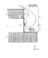
表面伝導型電子放出素子を用いた電子放出装置の一般的な例を図26(a)、図26(b)に示す。
【0010】
図26(a)、図26(b)において、2001は基板、2002,2003は電極、2004は導電性膜、2006は間隙、2007は素子の上方に配置されたアノード電極である。図26(a)は電子放出装置の断面模式図であり、図26(b)は、図26(a)の電子放出装置のアノード電極2007に照射される電子のビーム形状を示している。
【0011】
電子放出素子は、電極2002,2003間に駆動電圧Vfを与えらることで、間隙2006を電子がトンネリングし、その電子の一部が電子放出電流Ieとなりアノード電極2007に照射され、残る電子が電極2002,2003間を流れる素子電流Ifとなる。Ie/If×100[%]を効率(電子放出効率)と呼ぶ。表面伝導型電子放出素子のようなナノメートルオーダーの間隙を置いて対向する導電性部材間のトンネル現象を利用した電子放出素子では、Ifが非常に多くなる為、電子放出効率が低い。
【0012】
一方、上記した電子放出素子を用いて画像形成装置を形成する場合には、アノード電極2007に蛍光体を配置して、電子ビームを光に変換することにより、画像形成装置として使用される。しかし、近年、画像形成装置ではより高精細な表示が要求されている。したがって、高精細表示に必要な高精細な電子ビーム径を得る必要があった。さらに必要なのは、電子ビーム径が高精細表示に適した画素サイズでありながら、表示特性に必要な電子放出量を得ることである。そのために、電子放出効率を向上する事も要求される。
【0013】
そこで、本発明は上記の従来技術の課題を解決するためになされたもので、その目的とするところは、電子放出効率を向上させると同時に電子ビーム径の高精細化を両立する高性能な電子放出装置及び画像形成装置を提供することにある。
【0014】
【課題を解決するための手段】
上記目的を達成するために成された本発明の電子放出装置は、
基板と、
前記基板の表面上に配置された第1の導電性部材と、前記第1の導電性部材上に配置された絶縁層と、前記絶縁層上に配置された第2の導電性部材と、からなる積層体を有する電子放出素子と、
前記基板表面から離れて配置されたアノード電極と、
前記第1の導電性部材に印加する電位よりも高い電位を前記第2の導電性部材に印加する第1の電圧印加手段と、
前記第2の導電性部材に印加する電位よりも高い電位を前記アノード電極に印加する第2の電圧印加手段と、
を備える電子放出装置であって、
前記基板表面と実質的に平行な方向における前記絶縁層の端面上にて、前記第1の導電性部材の端部と前記第2の導電性部材の端部とが、間隙を置いて、対向して配置されており、
前記第1の導電性部材の端部と前記第2の導電性部材の端部とが対向する方向における、前記第2の導電性部材の長さがT1[nm]、
前記基板表面と実質的に平行な前記第1の導電性部材の表面から、前記第1の導電性部材の端部と前記第2の導電性部材の端部とが対向する方向に伸びる前記第1の導電性部材の長さがT3[nm]、
前記第2の導電性部材の仕事関数がφwk[eV]、
前記第1の導電性部材と前記第2の導電性部材間に印加される電圧がVf[V]、である際に、
T1<A×exp[B×(Vf−φwk)/(Vf)]
A=−0.50+0.56×log(T3),B=8.7
の条件を満たすことを特徴とする。
【0015】
また、上記目的を達成するために成された本発明の画像形成装置は、
複数の電子放出素子が配置された第1の基板と、
アノード電極と画像形成部材とを有する第2の基板と、
前記電子放出素子に電圧を印加するための第1の電圧印加手段と、
前記アノード電極に電圧を印加するための第2の電圧印加手段と、
を備える画像形成装置であって、
前記電子放出素子は、前記基板の表面上に配置された第1の導電性部材と、前記第1の導電性部材上に配置された絶縁層と、前記絶縁層上に配置された第2の導電性部材と、からなる積層体を有しており、
前記第1の電圧印加手段は、前記第1の導電性部材に印加する電位よりも高い電位を前記第2の導電性部材に印加し、
前記第2の電圧印加手段は、前記第2の導電性部材に印加する電位よりも高い電位を前記アノード電極に印加し、
前記基板表面と実質的に平行な方向における前記絶縁層の端面上にて、前記第1の導電性部材の端部と第2の導電性部材の端部とが、間隙を置いて、対向して配置されており、
前記第1の導電性部材の端部と第2の導電性部材の端部とが対向する方向における、前記第2の導電性部材の長さがT1[nm]、
前記基板表面と実質的に平行な前記第1の導電性部材の表面から、前記第1の導電性部材の端部と第2の導電性部材の端部とが対向する方向に伸びる前記第1の導電性部材の長さがT3[nm]、
前記第2の導電性部材の仕事関数がφwk[eV]、
前記第1の導電性部材と第2の導電性部材間に印加される電圧がVf[V]、である際に、
T1<A×exp[B×(Vf−φwk)/(Vf)]
A=−0.50+0.56×log(T3),B=8.7
の条件を満たすことを特徴とする。
【0016】
上記の条件を満たすことで、電子放出素子から放出される電子の散乱回数を低減することができ、さらに散乱のない電子を主成分とし利用できるので、電子放出効率を向上させると同時に電子ビーム径の高精細化を両立することができる。
【0017】
【発明の実施の形態】
以下に図面を参照して、この発明の好適な実施の形態を例示的に詳しく説明する。ただし、この実施の形態に記載されている構成部品の寸法、材質、形状、その相対配置などは、特に特定的な記載がない限りは、この発明の範囲をそれらのみに限定する趣旨のものではない。
【0018】
本実施の形態では、まず第1に電子放出効率の向上を行ない、かつ第2に電子ビーム径の高精細化を行なう。これらについて順次説明する。
【0019】
まず、従来の電子放出素子における電子の運動、及び本実施の形態による電子放出素子における電子の運動について説明をする。
【0020】
図26に示す様な平面型表面伝導型電子放出素子には、ナノメートルオーダーの間隙2006があり、この間隙を挟むように、高電位側の導電性部材(図26(b)の左側の導電性膜2004と電極2002)と、低電位側の導電性部材(図26(b)の右側の導電性膜2004と電極2003)と、が配置されている。
【0021】
この素子の電極2002,2003間に、電圧Vf[V]を印加すると低電位側の導電性部材の先端(図26(b)の右側の導電性膜2004の先端)から対向する高電位側導電性部材に向かって電子がトンネルし、電子が高電位側導電性部材の先端(図26(b)の左側の導電性膜2004の先端)で等方的に散乱すると考えられている。
【0022】
さらに、高電位側導電性部材の先端で散乱された電子の多くは高電位側導電性部材(図26(b)の左側の導電性膜2004および、あるいは電極2002)上で数回の弾性散乱(多重散乱)が繰り返され、間隙2006から特徴距離Xsまでの領域を越えた電子がアノード電極2007に到達する。
【0023】
ここで、特徴距離Xsは、
Xs=H×Vf/(π×Va)…(1)
で与えられる。なお、Hは電子放出素子とアノード電極2007間の距離であり、Vaはアノード電極2007への印加電圧である。
【0024】
例えば、Va=10[kV]、Vf=15[V]、H=2[mm]では、Xs=0.95〜約1μm程度である。
【0025】
特徴距離Xsは、高電位側導電性部材と真空中に形成された高電位側導電性部材と等しい電位面との交点から、間隙までの距離として理解されるものである。
【0026】
電子放出効率(以下、効率とする)ηは、電子がXsを越えるまでの間に、多重散乱によって高電位側導電性部材に一部吸収されることによる電子数の減少に支配されている。
【0027】
低電位側導電性部材の先端からトンネルした電子は、高電位側導電性部材の先端で等方散乱することにより、高電位電極の仕事関数(φwk)分のエネルギーを損失し、高電位側導電性部材上で再度散乱される。
【0028】
電子の散乱される割合の効率ηについては明らかでないが、一回につき0.1から0.5程度、通常0.3程度と見積もられている。
【0029】
このような効率ηが1以下である散乱機構であることから、真空中に取り出される電子の量は散乱回数により、べき乗で減少していくことがわかる。
【0030】
前記特徴距離Xsを通過した後の電子は、アノード電極2007に印加された電圧(Va[V])と素子の駆動電圧(Vf[V])とで形成された空間電位の影響を反映した電子軌道を描いてアノード電極2007に到達する。
【0031】
以下に、本実施の形態による電子放出素子の電子の運動と効率の向上について説明する。
【0032】
前述のようなメカニズムから、本発明では、電子放出効率を向上するために、電子の高電位側導電性部材上での散乱回数(落下の回数)を減少する構成とする。
【0033】
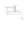
図1は本実施の形態の一例の電子放出素子の構成図である。図1(a)は平面図、図1(b)は図1(a)におけるA−A’線での断面図である。1は基板、2は低電位電極、3は絶縁層、4は高電位電極であり、5−1及び5−2は第1,第2の導電性膜、6は間隙である。
【0034】
間隙6を挟んで対向した第1の導電性膜5−1と第2の導電性膜5−2は、それぞれ電極2,4と接続される。第2の導電性膜5−2の一端は高電位電極4に接続され、第1の導電性膜5−1の一端は低電位電極2に接続されている。
【0035】
また、低電位電極2は、基板1の表面(主面)上に配置されている。このため、低電位電極2は、実質的に基板1の表面(主面)と平行な表面を有する。
【0036】
この素子を駆動して電子ビームを得る一般的な電子放出装置の配置例を図2に示す。ここで、7は素子の電極2,4間に駆動電圧(Vf[V])を印加するための電源(第1の電圧印加手段)である。8は、素子から放出された電子を引き上げて捕獲するためのアノード電極である。アノード電極8と電子放出素子との距離はHだけ隔てて配置されており、アノード電極8には、高圧電源(第2の電圧印加手段)9により、アノード電圧(Va[V])が印加される。上記電圧Vfは、低電位電極2に印加される電位と高電位電極4に印加される電位との差である。また、上記電圧Vaは、低電位側の電極2に印加される電位とアノード電極8に印加される電位との差であり、アノード電極8に印加される電位は高電位電極4に印加される電位よりも高い。
【0037】
ここで、アノード電極8と電子放出素子との距離Hは、基板1とアノード電極8との間の距離と考えて実質的に問題がない。
【0038】
高電位電極4と低電位電極2の間に印加される駆動電圧をVf[V]、そこに流れる電流はIf[A]、アノード電極8に印加される電圧をVa[V]、アノード電極8に電子が捕獲されて流れる電流はIe[A]となり、効率はη=(Ie/If)×100[%]で示される。
【0039】
さらに、この配置において電子放出部を拡大したものが図3である。
【0040】
図3中、6は間隙、4は高電位電極、2は低電位電極、5−1は低電位電極2に接続する第1の導電性膜、5−2は高電位電極4に接続する第2の導電性膜である。
【0041】
本発明においては、高電位側の高電位電極4と第2の導電性膜5−2とを含めて「高電位側導電性部材」と呼ぶ。また、低電位側の低電位電極2と第1の導電性膜5−1とを含めて「低電位側導電性部材」と呼ぶ。
【0042】
したがって、高電位側の導電性部材と低電位側の導電性部材は、絶縁層3を間に挟んだ積層構造となっているといえる。そして、この積層体(高電位側導電性部材と絶縁層と低電位側導電性部材)は基板1の表面(主面)上に配置され、その積層方向が、基板1の表面に対して実質的に垂直に配置されている。
【0043】
このため、図3、図1に示すように、本発明の電子放出素子においては、基板1の表面と実質的に平行な方向に置ける絶縁層3の端面上にて、第1(低電位側)の導電性部材の端部(第1の導電性膜5−1の端部)と第2(高電位側)の導電性部材の端部(第2の導電性膜5−2の端部)とが、間隙6を置いて、対向して配置されている。
【0044】
この構造を換言すると、基板1の表面と実質的に平行な方向における絶縁層3の端面上に、第1(低電位側)の導電性部材の一端(第1の導電性膜5−1の一端)と第2(高電位側)の導電性部材の一端(第2の導電性膜5−2の一端)とが配置されており、そして、各々の先端が間隙6を置いて対向して配置されている。
【0045】
尚、詳しくは後述するが、上記「基板1の表面と実質的に平行な方向に置ける絶縁層3の端面」と、基板1の表面との成す角度は、45度以上100度以下が好ましく、さらには90度±10度以下であることが特に好ましい。
【0046】
そして、この間隙6において、後述するように、低電位側導電性部材先端から、高電位側導電性部材先端に向けて電子がトンネルし、その結果、電子が放出される。
【0047】
図3中、T1、T2、T3は、素子部の電位から決定される各々の長さであり、単なる電極厚さ、絶縁層厚さなどとは異なるものである。
【0048】
即ち、T1は間隙6の端から高電位側導電性部材の屈曲した部分までの距離、T2は低電位側第1の導電性膜5−1と高電位側第2の導電性膜5−2とが対向する方向(図3のZ方向)における間隙6の幅、T3は間隙6の端から低電位側導電性部材の屈曲した部分までの距離である。
【0049】
換言すると、T1は第1の導電性膜5−1と第2の導電性膜5−2とが、間隙6を介して対向する方向(図3のZ方向)における、第2の導電性膜5−2の長さである。T2は第1の導電性膜5−1と第2の導電性膜5−2とが対向する方向(図3のZ方向)における、第1の導電性膜5−1の長さである。
【0050】
換言すると、T1は絶縁層3の側面(基板1の表面と実質的に平行な方向に置ける絶縁層3の端面)において、第1の導電性部材の端部と第2の導電性部材の端部とが対向する方向における、第2の導電性部材の長さということができる。
【0051】
また、前述した様に、本発明の素子では、実質的に基板1の表面(主面)と平行な表面を低電位電極2が有するため、T3は基板1表面と実質的に平行な第1の導電性部材表面から、第1の導電性部材の端部と第2の導電性部材の端部とが絶縁層3の側面(基板1の表面と実質的に平行な方向に置ける絶縁層3の端面)において対向する方向に、伸びる第1の導電性部材の長さという事もできる。
【0052】
あるいは、同様に、本発明の素子では、実質的に基板1の表面(主面)と平行な表面を低電位電極2と低電位側導電性膜5−1とが有するため、T3は基板1表面と実質的に平行な低電位側導電性膜5−1表面から、第1の導電性膜5−1の端部と第2の導電性膜5−2の端部とが対向する方向に伸びる第1の導電性膜5−1の長さという事もできる。
【0053】
本発明は、第1に高効率を得るのに最も適した領域長を鋭意検討したものであり、そのために、主としてT1の長さを定めたものである。
【0054】
本実施の形態において、電極2,4間に駆動電圧Vf[V]を印加すると、従来の平面型電子放出素子と同様の放出機構で電子が放出される。すなわち、低電位側導電性部材の先端から、対向する高電位側導電性部材に向けて電子がトンネルし、高電位側導電性部材の先端部で等方的に散乱する。高電位側導電性部材の先端部から散乱された電子の多くは、弾性散乱を1回から数回にわたって高電位側導電性部材上で繰り返す。
【0055】
しかしながら、図3に示した垂直型と、図26で示した従来の平面型では、アノード電極8の電位と素子の電位で構成される空間電位の分布が異なる。そのため、図3に示す様に、高電位側導電性部材の先端部で等方的に散乱された電子のうちの一部は、再び高電位電極4で散乱することなく、高電位電極4の屈曲した端部の上方に到達し、そのままアノード電極8へと到達するものが現れる。
【0056】
このように、高電位側導電性部材上での散乱を抑制する事が、電子放出効率向上に重要となる。
【0057】
従来の平面型の場合、Okuda et al, “Electron Trajectory Analysis of Surface Conduction Electron Emitter Displays(SEDs)”, SID 98 DIGEST,p.185−188などに開示されているように、電子放出効率は、散乱電子の到達分布と特徴距離XsまたはXs〜=γ×Xs(γは係数で=0.67)とで決定される、と想定されている。
【0058】
また、散乱電子の到達分布は、電子の最大飛翔距離に関係し、そして、間隙6の幅D(図3ではT2と定義している)と、駆動電圧と仕事関数(本発明では高電位側導電性部材の仕事関数φwkと定義している)とで決定される係数Cで正規化される。
【0059】
本発明の電子放出素子における効率には、電子の最大飛翔距離が関係している。だだし、前述のようにアノード電極8と素子の駆動電圧Vfで構成される空間電位分布が平面型とは異なり、複雑となる。
【0060】
前記特徴距離Xs以下の領域内に高電位側導電性部材の屈曲した部分が構成されると、Xsに依存せず、主としてT1の距離で効率が決定される。
【0061】
さらに、T1が、1回目の散乱(高電位側導電性部材の先端で散乱した後の1回目の散乱)までの最大飛翔距離未満となることで、散乱なしの電子(高電位側導電性部材の先端で散乱するだけで、それ以降の散乱を起こさない電子)が存在する。
【0062】
以上から、本発明では、垂直型での電子の挙動、特に散乱の挙動の詳細な検討を行った結果、高電位側導電性部材に用いた材料(第2の導電性膜材料)の仕事関数φwkと駆動電圧Vfの関数として、さらに、T1,T3の距離の関数、すなわち電子放出部近傍の形状を工夫する事により、効率を大幅に向上する電子放出素子を得た。
【0063】
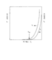
以下、図4、図5を用いてより詳細に本発明の電子放出素子を説明する。図4(a)は、T1と効率ηの相関を示すグラフの一例であり、図4(b)は、図4(a)の電子放出効率ηを、電子の散乱回数別に示したグラフである。
【0064】
図4において横軸は、T1[nm]であり対数表示となっている。縦軸は、図4(a)では効率ηである。図4(b)の縦軸は散乱回数別の効率である。
【0065】
図4(a)に示すように、効率ηは、T1が大きくなるにつれて急激に低下する第1の領域と、その後の効率低下が減少する第2の領域に別れている。これは、到達する電子の散乱回数と相関がある。
【0066】
第1の領域は、散乱なしの電子(高電位側導電性部材の先端で散乱するだけで、それ以降の散乱を起こさない電子)がアノード電極8に到達する電子の大半を占める領域であり、それ以降の第2の領域は、複数回の散乱を経た電子が大半を占める領域となっていると考えられる。
【0067】
図4(b)に示す様に、散乱なしの電子(高電位側導電性部材の先端で散乱するだけで、それ以降の散乱を起こさない電子)の到達領域はT1maxで示され、図4(a)では1段めの効率低下曲線をη=0へと外挿した点として表される。
【0068】
また、第1の領域と第2の領域との交点は、図4(b)においてT1max’で示され、この点は、主たる散乱回数が変わる変曲点であると考えられる。
【0069】
図5(a)に、Vf(素子の駆動電圧)およびφwk(高電位側導電性部材の仕事関数)とT1maxとの関係をグラフで示した。横軸は線形表示、縦軸は対数表示である。駆動条件が決定されると、効率向上に効果の期待できる、すなわち、散乱なしの電子がアノード電極8に到達可能な形状が決定できることがわかる。
【0070】
図5(a)の横軸で表した(Vf−φwk)/Vfの説明を図5(b)に示した。
【0071】
駆動条件をVfとすると、電子放出部(間隙6)近傍には、空間を等分するような電場が形成される。(Vf−φwk)の等電位面は図5(b)太線で示した位置となり、この面が放出された電子をそれ以上低電位側には到達させない壁となっているといえる。
【0072】
T1の変化は、この等電位面の位置を変化させると共に、電場の方向と強さを変化させ、電子の軌道を変化させることになる。この電場が電子に大きな作用与えるのは、特徴距離Xsもしくは間隙幅T2の200倍程度と概算されている。
【0073】
本実施の形態においては、間隙幅T2は数nmから数十nmであり、T1を数十nmから数百nmに設定することで、ちょうど散乱電子の飛翔に大きく影響を与える領域になり、形状の効果が期待できる。
【0074】
また、図5(a)グラフ中には、T1maxのT3の依存性を示した。T1と同様にT3の形状も間隙周辺の電場を変化させる要因であることがわかる。
【0075】
ただし、T1は小さい程効率の向上に効果があるが、T3は大きい程効率の向上に効果があり、T3=∞でほぼ一定となるという違いがある。
【0076】
図5(a)のグラフから、T1maxに関して、
T1max=A×exp[B×(Vf−φwk)/(Vf)]…(2)
A=−0.78+0.87×log(T3)
B=8.7
の式が導かれる。
【0077】
ここで、T1,T3は距離(単位はnm)、φwkは高電位側導電性部材の仕事関数の値(単位はeV)、Vfは駆動電圧(単位はV)、AはT3の関数、Bは定数である。
【0078】
さらに、検討した結果、前述の主たる散乱回数が変化する変曲点T1max’は、(2)式のAの関数の係数の変化で近似できることもわかった。
【0079】
したがって、
T1max’=A’×exp[B×(Vf−φwk)/(Vf)]…(2)’
A’=−0.50+0.56×log(T3)
B=8.7
の式が導かれる。
【0080】
これまで説明したように電子放出効率には、散乱に関わるパラメータとしてT1が重要であり、T1を(2)式、さらに好ましくは(2)’式の範囲に設定すれば、著しく効率向上の効果が得られることがわかり、本発明ではT1を(2)’式の範囲に限定した。
【0081】
さらに、図6に本発明による構成の電子放出素子の電子放出特性を従来の平面型電子放出素子と比較して示した。本発明による電位放出素子では、低いVa側で、効率の変化が大きく上昇している。したがって、本発明の構成を実現することで、より低いVaの駆動を可能することもできる。
【0082】
ここで、本発明による構造を作製するためには、電極2,4及び絶縁層3の積層の膜厚の制御が重要である。特に、絶縁層3及び高電位電極4の膜厚の制御が必要となる。
【0083】
一方、本発明による構造では、数μm程度の微細な形状パターンを持たず、従ってパターン形成のための高価な製造装置が必要ではない。例えば、フォトリソグラフィー工程を使用する場合でも、より簡易な製法が選択できる。また、x方向及びy方向に対する位置合わせ精度も比較的にゆるく設定可能である。
【0084】
次に、本発明の電子放出素子による、電子ビーム径の高精細化について説明する。
【0085】
従来の平面型の電子放出素子の電子ビーム径については、SID98Digest、Okuda,et.alによると、
Lh?4×Kh×H×√(Vf/Va)+L0…(3a)
Lw?2×Kw×H×√(Vf/Va)…(3b)
以上の式で近似される。
【0086】
ここで、Lhはy方向の電子ビーム径、Lwはx方向の電子ビーム径であり、L0はy方向の素子長である。また、Kh、Kwは定数で、Khは0.8〜0.9、Kwは0.8〜1.0であるとされている。
【0087】
また、Va=10kV、H=3mmにおいては、Lhから0.5mm、Lwから0.25mmなるサイズが得られている。
【0088】
本発明の素子においては、T1を一定値より小さくする構成を提案するものであるから、アノード電極側から眺めた場合には、その距離は十分小さく、従来の平面型の素子と同様に、一般的に(3a)、(3b)式が適用できる。ただし、Kh、Kwの係数に違いが見られ、特にx方向の電子ビーム径の係数であるKwの値が小さくなり、電子ビーム径の高精細化が実現される。
【0089】
図7に本発明による素子の散乱回数別の電子の最大到達位置を示した。
【0090】
電子は、高電位電極上に形成される曲がった空間電位の影響によりx方向に曲げられるが、高電位電極上で散乱が起こるとその方向が変わるために、電子ビームの到達位置は変化し、その広がりは扇状の内側となる。ただし、その強度分布は一様でなく、散乱回数が少ない程、扇状の外縁部に、またその中でもy方向の原点付近に偏よっている傾向がある。
【0091】
一方、散乱のない電子(高電位側導電性部材の先端で散乱するだけで、それ以降の散乱を起こさない電子)は、放出時の方向性を保持したまま、駆動電圧とアノード電圧とで決定される空間電位によりその軌道が曲がるだけであるので、特定の軌跡をもった線状に到達する。
【0092】
本発明による構成では、アノード電極に到達する電子の平均的な散乱回数を減少させることで、電子ビームの強度分布を扇状の外縁部に集中させることが可能となる。その結果、x方向、およびy方向の相対的な強度分布を変化させることができる。
【0093】
電子ビーム形状は、通常、ピーク強度に対する強度比が十分減衰した領域の長さで定義されるものであるから、強度分布が変わることで、電子ビーム形状も縮小させることができる。
【0094】
また、上記(2)’式で定義したような、アノード電極に到達する電子の主成分を散乱なしの成分とする形状を選択すれば、さらに図7で示したごく狭い領域内に電子ビームを集めることができ、Kw、Khを減少させることができる。
【0095】
以上の本実施の形態で示すように、本発明は、散乱回数を低減し、散乱のない電子(高電位側導電性部材の先端で散乱するだけで、それ以降の散乱を起こさない電子)を主成分として利用することで、高い電子放出効率と高精細な電子ビーム径の収束の両立が可能である。
【0096】
さらに、好ましいT1の適用範囲について記す。
【0097】
前述した散乱回数の説明から、効率ηの点からは、T1は理想的に0であることが要求される。しかしながら、T1は電位を与えるための電極の役割を有す必要がある。したがって、最低限の厚さは必要となる。薄い場合には寄生抵抗となり、間隙部に係る電圧の減少となって現れ、さらに、耐熱性の低下により、素子劣化の要因にもなり得る。
【0098】
また、T1が0に近づくと、間隙が絶縁層の側壁でなく、絶縁層の端部で、アノード電極方向に向かった開口で形成される場合があったが、この場合、効率、電子ビーム径ともに所望の結果が必ずしも得られず、素子間のばらつきが増大した。
【0099】
これは、間隙の方向に係るものであり、本実施の形態においては、間隙が絶縁層の側壁に垂直に開口していることが前記条件式の成立の際の用件ともいえる。
【0100】
したがって、本発明における実用的なT1は、少なくとも10nm程度の長さが必要である。
【0101】
また、T1を極端に薄くした場合、アノード電圧Vaによっては、高電位側導電性部材の屈曲する部分までの側面での散乱は抑制されるが、一方、その後、高電位側導電性部材の上面部(アノード電極と対向する面)で散乱する成分も現れ、かえって効率ηが低くなり、ビーム径Lwが広がることがわかった。
【0102】
上記の説明を図8(a)に示した。これは、効率が、高電位側導電性部材の屈曲する部分を散乱なしで通過する電子の方向成分に依存することを示している。
【0103】
すなわち、図8(b)に示すように、T1がある程度の厚みをもった方が、アノード電極方向にむかう角度のうち低角度の成分を多重散乱によって抑制し、直接アノード電極方向に向かう成分を限定することにより、より高精細な電子ビームが可能となると考えられる。
【0104】
このことより、図4(a)のグラフで、T1が薄くなっても、効率、電子ビーム径はそれほど向上せず、それ以上の特性の向上は見られない。この特性に飽和が見られた領域は、アノード電圧Vaの条件にもよるが、T1≦T1max’/2であるといえる。
【0105】
この領域を使用すれば、電子放出部の位置のばらつきに対する特性のばらつきを緩和させることもでき、均一化に有利である。
【0106】
したがって、本実施の形態における好ましいT1は、0<T1<T1max’であり、さらに好ましいのは、0<T1≦T1max’/2である。一方、実用的に決定されるのは、10nm≦T1<T1’maxであり、より好ましくは、10nm≦T1≦T1max’/2である。
【0107】
さらに、本発明における(2)、(2)’式の成立するための必要な要件について追記する。
【0108】
図9に本発明の電子放出素子が傾斜をもった絶縁層の側壁に形成された場合について示した。また、図10に傾斜角度と効率および電子ビーム径の関係を示すグラフを示した。
【0109】
これまでは、断面として、基板1平面に対し、垂直な断面を持つ絶縁層3の側面に形成される場合の電子放出素子について説明し、条件を決定した。しかし、素子の作製工程において、絶縁層3および高電位電極4の断面を、完全な垂直に形成することは難しく、一般には図9で示したように基板1表面(電極2表面)に対してある角度θを持って形成されるのが普通である。
【0110】
傾斜が存在する場合でも、θが90度に近い場合(90度±10度以内)は、図9(b)に示す様に、断面に対し平行な長さをT1’、T2’、T3’と置き換えることで、前述(2)、(2)’の用件が実質的に成り立つ。
【0111】
また、図10には、いろいろな傾斜角度でのビーム径と効率を示した。傾斜角度θが45度未満では電子ビーム径Lwが急激に減少するとともに、効率ηも減少する。また、θが100度よりも大きいと、電子ビーム径Lwは大きくならないが、効率ηが急激に減少する。
【0112】
これは、傾斜角度θが45度未満では単なる長さの変化ではなく、傾斜自体が空間電位を変えてしまい、その特性がT1もしくはT3に依存せず、すなわち従来の平面型に近づくことを示している。また傾斜角度θが100度よりも大きいと、傾斜のために散乱回数がかえって増大してしまう。
【0113】
したがって、好ましい適用範囲は、傾斜角度45度以上100度以下であり、さらに好ましくは、90度±10度以内である。
【0114】
本発明においては、電子放出部近傍の形状が重要であることは説明したが、当然、電子軌道の及ぼす範囲としてさらに広範囲にわたる電位分布も重要である。それらのパラメータとして重要なものとしては、アノード電極からみたときの、電子放出部から高電位側導電性部材終端(x、y各方向)、電子放出部から低電位側導電性部材終端(x、y各方向)までの距離とその厚さ(z方向)がある。また、特に、x方向の距離は重要である。
【0115】
厚さが均一な場合には、電位領域のサイズの目安として、前述の特徴距離Xsが、参考となる。すなわち、x、y方向とも特徴距離Xsの15倍以上であれば、本実施の形態の効果を得るのに十分である。また、少なくとも、y方向には特徴距離Xsの1.5倍以上、望ましくは5倍以上あれば、本実施の形態の適用範囲が若干ずれるが、高効率、電子ビーム径の高精細の効果が得られる。
【0116】
x方向に対し、領域長に充分な長さが必要なのは、本実施の形態による構成が、x方向の電位分布の影響をより大きく受ける電位分布であるためである。
【0117】
厚さ方向に変化がある場合には、さらに注意が必要であるが、適宜、電子軌道を考慮して決定することで、本発明の効果を生かすことは十分可能である。
【0118】
以上のように、本発明の構成とした場合には、電子放出効率ηの向上が図られると共に、電子ビーム径の収束による高精細化を図ることができる。
【0119】
x方向の電子ビーム径の係数としては、Kwとして0.3〜、y方向のビーム径の係数としては、Khとして0.6〜が可能である。
【0120】
以上述べた本発明の電子放出素子、並びにそれを用いた電子放出装置および画像形成装置について、更に好ましい実施形態および作成方法を挙げて詳述する。
【0121】
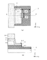
図11、図12は本発明による電子放出素子の一例を示す模式図、図11(a)は平面図、図11(b)は図11(a)のA−A’断面図、図12は図11の素子の電子放出部近傍を拡大して示した模式図である。図13、図14には、本発明の電子放出素子の製造方法の一例を示す。
【0122】
図11において、図1と同じ部材には、同じ番号を付記した。1は基板、2は低電位電極、3は絶縁層、4は高電位電極、5−1,5−2は第1,第2の導電性膜、6は間隙である。
【0123】
111は、第2の絶縁層であり、高電位電極4と低電位電極2をそれぞれx方向に伸びる配線、y方向に伸びる配線としてマトリクス状に形成した場合に、その交点の容量を低減するために積層される場合がある。
【0124】
図11に示すように、素子はy方向にL0の長さを有している。また、x方向には、電子放出部(絶縁層3の側壁)から垂直方向に延長した高電位電極幅L1、低電位電極幅L2となっている。
【0125】
高電位電極幅L1、低電位電極幅L2は、前述のように本発明の効果を得るために、一定の長さ以上が必要である。
【0126】
例えば、駆動電圧Vf、アノード電圧Va、素子−アノード電極8間距離Hとした場合、その特徴距離Xs=(H×Vf)/(π×Va)であり、好ましくは特徴距離Xsの15倍以上の幅を持つ電極を用いることが必要である。
【0127】
基板1としては、その表面を十分に洗浄した、石英ガラス、Na等の不純物含有量を減少させKなどに一部置換したガラス、青板ガラス及びシリコン基板等にスパッタ法等によりSiO2を積層した積層体、アルミナ等のセラミックスの絶縁性基板が挙げられる。
【0128】
低電位電極2は一般的に導電性を有しており、蒸着法、スパッタ法等の一般的真空成膜技術、フォトリソグラフィー技術により形成される。
【0129】
電極の材料は、例えば、Be、Mg、Ti、Zr、Hf、V、Nb、Ta、Mo、W、Al、Cu、Ni、Cr、Au、Pt、Pd等の金属、合金材料もしくは後述する導電性膜5と同一の材料から適宜選択される。前記低電位電極2の厚さとしては、数十nmから数mmの範囲で設定され、好ましくは数十nmから数百μmの範囲で選択される。
【0130】
絶縁層3は、スパッタ法等の一般的な真空成膜法、熱酸化法、陽極酸化法等で形成され、その厚さとしては、数nmから数十μmの範囲で設定され、好ましくは数十nmから数μmの範囲から選択される。望ましい材料としてはSiO2、SiN、Al2O3、CaF、などの高電界に絶えられる耐圧の高い材料が望ましい。
【0131】
高電位電極4は、低電位電極2と同一材料でも異種材料でも良く、好ましくは耐熱性材料が望ましい。またその厚さは、効果を得るため、間隙位置と共に重要なパラメータとなる。したがって、数nmから数百nmの範囲で設定される。また、後述の第1,第2の導電性膜5−1,5−2と兼ねる場合もある。
【0132】
第1,第2の導電性膜5−1,5−2は、スパッタ法等の一般的な真空成膜法等で形成される。
【0133】
第1,第2の導電性膜5−1,5−2に用いる材料としては、Pd,Ru,Ag,Au,Ti,In,Cu,Cr,Fe,Zn,Sn,Ta,W,Pt等の金属、およびそれらの合金、PdO,SnO2,In2O3,PbO,Sb2O3等の酸化物、HfB2,ZrB2,LaB6,CeB6,YB4,GdB4等の硼化物、TiC,ZrC,HfC,TaC,SiC,WC等の炭化物、TiN,ZrN,HfN等の窒化物、Si,Ge等の半導体、カーボン等である。その抵抗値は、103〜107Ω/□のシート抵抗値を示す。
【0134】
第1,第2の導電性膜5−1,5−2に、間隙6を作製するには、例えば、“フォーミング処理”と呼ばれる手法が用いられる。“フォーミング処理”は、連続した導電性膜に電流を流すことで発生するジュール熱によって、連続した導電性膜の一部に間隙を形成する工程である。
【0135】
後述の“活性化工程”を行わない場合には、導電性膜の仕事関数(φwk)が重要となる。
【0136】
さらに、“フォーミング処理”を終えた素子に“活性化工程”を施すことにより、図12に示すように、間隙6内の絶縁層3上および導電性膜5上に、炭素を有する膜(カーボン膜)10を形成する場合がある。
【0137】
上記カーボン膜10は、例えばグラファイト(いわいるHOPG,PG,GCを包含する。HOPGはほぼ完全なグラファイトの結晶構造、PGは結晶粒が20nm程度で結晶構造がやや乱れたもの、GCは結晶粒が2nm程度になり結晶構造の乱れがさらに大きくなったものを指す。)、非晶質炭素(アモルファス炭素及び、アモルファス炭素と前記グラファイトの微結晶の混合物を指す)を含む導電性の膜である。
【0138】
本工程によりカーボン膜10を被覆した場合には、図12に示す第1の導電性膜5−1と第2の導電性膜5−2とが対向する方向におけるカーボン膜10の長さは、T1及びT3に加算される。またカーボン膜10の膜厚は、比較的に薄い方が良く、数nmから数十nm以下の範囲とするのが好ましい。
【0139】
これにより、図12に示すように、上記活性化工程により、間隙6よりも狭い間隙7が形成される。この間隙7の長さがT2となる。
【0140】
なお、ここでは、活性化工程で形成する膜10をカーボン膜としたが、本発明においては、その他の導電性の材料からなる膜であってもよい。
【0141】
そして、活性化工程を行なった素子においては、前記第1の導電性膜5−1と電極2に加えて、第1の導電性膜5−1に接続したカーボン膜10を含めて低電位側導電性部材と呼ぶ。また同様に、活性化工程を行なった素子においては、前記第2の導電性膜5−2と電極4に加えて、第2の導電性膜5−2に接続したカーボン膜10を含めて高電位側導電性部材と呼ぶ。
【0142】
活性化工程で、間隙6付近およびその周辺部に導電性膜とは別の材料が形成された場合、その仕事関数φwkは、本実施の形態のパラメータとなるため重要である。
【0143】
通常、高電位側導電性部材の仕事関数φwkは、活性化工程を行った素子の場合、炭素の仕事関数である、φwk=5eVが適用される。活性化工程を行わなかった素子の場合には、高電位側の第2の導電性膜5−2の材料の仕事関数が適用される。
【0144】
次に図11に示した電子放出素子の製造工程について図13、図14を用いて説明する。
【0145】
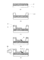
(1)絶縁性基板1の表面(第1の主面)上に低電位電極2の材料を堆積し、ホトリソグラフィー等による適当な方法で好ましい形状にエッチングを行い低電位電極2を形成する。(図13(A))。
【0146】
(2)第2の絶縁層となる層間絶縁層111の材料を堆積し、ホトリソグラフィー等による適当な方法で好ましい形状にエッチングし、低電位電極2を露出させ、層間絶縁層111を形成する(図13(B))。
【0147】
(3)絶縁層3の材料、高電位電極4の材料を堆積し、ホトリソグラフィー等による適当な方法で好ましい形状にエッチングし、再び低電位電極2を露出させ、絶縁層3および高電位電極4を作製する(図13(C))。
【0148】
高電位電極4の形成手法としては、フォトレジストのスピンコーティング、マスクパターンの露光及び現像を行い、ウェットエッチングもしくはドライエッチングで絶縁層3及び高電位電極4の一部が取り除かれる。エッチング工程は平滑かつ垂直なエッチング面が望ましく、それぞれの電極及び絶縁層の材料に応じて、エッチング方法を選択すれば良い。
【0149】
(4)次に、導電性膜5の材料を堆積し、ホトリソグラフィー等による適当な方法で好ましい形状にする(図13(D))。
【0150】
(5)さらに前述した“フォーミング処理”により、導電性膜の一部に間隙6を作製する(図13(E))。
【0151】
フォーミング工程の一例としては、低電位電極2と高電位電極4間にパルス発生器131で電圧を印加し、導電性膜5の一部に間隙6を作製する方法がある。このフォーミング工程により、図12などに示す様に、高電位電極4に電気的に接続されている第2の導電性膜5−2と、低電位電極2に電気的に接続されている第1の導電性膜5−1とに分離される。
【0152】
(6)さらに、活性化工程を行う。その一例を図14に示す。活性化工程は、例えば、炭素化合物のガスを含有する雰囲気下で、両極性のパルス電圧の印加を繰り返すことで行うことで、図12に示す様にカーボン膜10を形成する。カーボン膜10の形成領域は、各部材の大きさや、活性化工程において印加する電圧値によっても異なり、例えば図15に示す様に、各導電性膜5−1,5−2の大半を覆うように形成することもできる。
【0153】
上記炭素化合物の雰囲気は、例えば油拡散ポンプやロータリーポンプなどを用いて真空装置141内を排気した場合に雰囲気内に残留する有機ガスを利用して形成することができる他、イオンポンプなどにより一旦十分に排気した真空中に適当な有機材料142を導入することによっても得られる。
【0154】
このときの好ましい有機材料142のガス圧は、真空装置141の形状や、有機材料142の種類などにより異なるため場合に応じ適宜設定される。
【0155】
適当な有機材料142としては、アルカン、アルケン、アルキンの脂肪族炭化水素類、芳香族炭化水素類、アルコール類、アルデヒド類、ケトン類、アミン類、ニトリル類、フェノール、カルボン、スルホン酸等の有機酸類等を挙げることが出来、具体的には、メタン、エタン、プロパンなどCnH2n+2で表される飽和炭化水素、エチレン、プロピレンなどCnH2n等の組成式で表される不飽和炭化水素、ベンゼン、トルエン、メタノール、エタノール、ホルムアルデヒド、アセトアルデヒド、アセトン、メチルエチルケトン、メチルアミン、エチルアミン、フェノール、ベンゾニトリル、アセトニトリル、蟻酸、酢酸、プロピオン酸等が使用できる。この処理により、雰囲気中に存在する有機材料142から、炭素あるいは炭素化合物が素子上に堆積物としてカーボン膜10が積層、被覆される。
【0156】
この活性化工程を行うことで、図12に示す様に、導電性膜5−1,5−2の間に形成された間隙6内の絶縁層3上および導電性膜5−1,5−2上にカーボン膜10が形成される。そして同時に、間隙6よりも狭い間隙7が、カーボン膜10によって形成される。
【0157】
以上の工程により、本発明の電子放出素子が形成される。
【0158】
次に、本発明の電子放出素子の応用例について以下に述べる。電子放出素子を複数個基体上に配列し、例えば電子源あるいは画像形成装置が構成できる。
【0159】
電子放出素子の配列については、種々のものが採用できる。一例として、並列に配置した多数の電子放出素子の個々を両端で接続し、電子放出素子の行を多数個配し(行方向と呼ぶ)、この配線と直交する方向(列方向と呼ぶ)で、該電子放出素子の上方に配した制御電極(グリッドとも呼ぶ)により、電子放出素子からの電子を制御駆動するはしご状配置のものがある。
【0160】
これとは別に、電子放出素子をx方向及びy方向に行列状に複数個配し、同じ行に配された複数の電子放出素子の電極の一方を、x方向の配線に共通に接続し、同じ列に配された複数の電子放出素子の電極の他方を、y方向の配線に共通に接続するものが挙げられる。このようなものは所謂単純マトリクス配置である。
【0161】
まず単純マトリクス配置について以下に詳述する。本発明の電子放出素子の特性を図16に示した。電子放出素子からの放出電子は、しきい値電圧Vth以上では、電極間に印加するパルス状電圧の波高値と幅で制御できる。一方、しきい値電圧Vth以下では、殆ど放出されない。
【0162】
この特性によれば、多数の電子放出素子を配置した場合においても、個々の素子に、パルス状電圧を適宜印加すれば、入力信号に応じて、電子放出素子を選択して電子放出量を制御できる。
【0163】
以下この原理に基づき、本発明の電子放出素子を複数配して得られる電子源について、図17を用いて説明する。図17において、171は電子源基体、172はx方向配線、173はy方向配線である。174は本発明の電子放出素子、175は結線である。
【0164】
m本のx方向配線172は,Dx1,Dx2,…Dxmからなり、真空蒸着法、印刷法、スパッタ法等を用いて形成された導電性金属等で構成することができる。配線の材料、膜厚、幅は、適宜設計される。y方向配線173は、Dy1,Dy2,…Dynのn本の配線よりなり、x方向配線172と同様に形成される。これらm本のx方向配線172とn本のy方向配線173との間には、不図示の層間絶縁層が設けられており、両者を電気的に分離している(m,nは,共に正の整数)。
【0165】
不図示の層間絶縁層は、真空蒸着法、印刷法、スパッタ法等を用いて形成されたSiO2等で構成される。例えば、x方向配線172を形成した基体171の全面或は一部に所望の形状で形成され、特に、x方向配線172とy方向配線173の交差部の電位差に耐え得るように、膜厚、材料、製法が適宜設定される。
【0166】
x方向配線172とy方向配線173は、それぞれ外部端子として引き出されている。また、電子放出素子174を構成する一対の電極(不図示)は、m本のx方向配線172とn本のy方向配線173と電気的に接続されている。
【0167】
配線172と配線173を構成する材料、結線175を構成する材料及び一対の素子電極を構成する材料は、その構成元素の一部あるいは全部が同一であっても、またそれぞれ異なってもよい。これら材料は、例えば前述の電極の材料により適宜選択される。素子電極を構成する材料と配線材料が同一である場合には、素子電極に接続した配線は素子電極ということもできる。
【0168】
x方向配線172には、x方向に配列した電子放出素子174の行を選択するための走査信号を印加する不図示の走査信号印加手段が接続される。一方、y方向配線173には、y方向に配列した放出素子174の各列を入力信号に応じて、変調するための不図示の変調信号発生手段が接続される。各電子放出素子に印加される駆動電圧は、当該素子174に印加される走査信号と変調信号の差電圧として供給される。
【0169】
上記構成においては、単純なマトリクス配線を用いて、個別の素子を選択し、独立に駆動可能とすることができる。
【0170】
このような単純マトリクス配置の電子源を用いて構成した画像形成装置について、図18を用いて説明する。
【0171】
図18は、画像形成装置の表示パネルの一例を示す模式図であり、171は電子放出素子を複数配した電子源基体、181は電子源基体171を固定したリアプレート、186はガラス基体183の内面に蛍光膜184とメタルバック185等が形成されたフェースプレートである。
【0172】
182は支持枠であり、該支持枠182には、リアプレート181、フェースプレート186がフリットガラス等を用いて接続されている。
【0173】
外囲器187は、例えば大気中、真空中あるいは、窒素中で、400〜500度の温度範囲で10分以上焼成することで、封着して構成される。外囲器187は、上述の如く、フェースプレート186、支持枠182、リアプレート181で構成される。
【0174】
リアプレート181は主に電子源基体171の強度を補強する目的で設けられるため、電子源基体171自体で十分な強度を持つ場合は別体のリアプレート181は不要とすることができる。即ち、基体171に直接支持枠182を封着し、フェースプレート186、支持枠182及び基体171で外囲器187を構成しても良い。
【0175】
一方、フェースプレート186、リアプレート181間に、スペーサーとよばれる不図示の支持体を設置することにより、大気圧に対して十分な強度をもつ外囲器187を構成することもできる。
【0176】
図19にフェースプレート186の例を示す。図19(a)は、ストライプ構造、(b)はマトリクス構造である。
【0177】
本発明における画像形成装置では、高精細表示が可能となるため、これらの配列の形態とピッチが選択できる。また、本発明の電子放出素子では、特にx方向の電子ビーム径を小さくできることから、図19(a)で示したストライプ構造に対して有利な構成である。
【0178】
フェースプレート186はそれぞれ、蛍光体192、黒色部材191で構成されている。黒色部材191、蛍光体192の材料としては、一般的なものが使用可能である。
【0179】
ただし、一般的に、電子放出素子において電子ビームのビーム径を小さくした場合においても、蛍光体ではそれに加えて、さらに広がりのある光のビームとして変換される。したがって、高精細表示を目指す場合には、蛍光体としても、適宜、ビーム広がりを考慮して、材料および、膜厚を選択される必要がある。
【0180】
フェースプレート186とリアプレート181の間の距離は、支持枠182、もしくは、スペーサー(不図示)により、一定の距離Hで保持される。平板型表示装置のための距離Hとしては、一般に、数μm〜数mmが選択される。
【0181】
その距離Hは、前述(3a)、(3b)式で示されるように、電子放出素子からのビームが蛍光体へと到達する場合の到達位置、および電子ビーム径の関数であり、Hが小さい程、高精細なビーム径が得られる。ただし、Hが小さいと、真空を保持するのが難しくなるため、大きなサイズの画像形成装置には不向きとなる。
【0182】
一方、(3a)、(3b)式は、Va>>Vfの際の成立し、画像形成装置としては一般的にVaは1kV以上30kV以下の値が選択される。
【0183】
しかし、Hを小さくし、かつ、Vaを高くすると、放電を起こし易くなるため、その作製方法に配慮が必要となる。したがって、本実施の形態において、好ましい範囲としては、Hは0.1mm以上5mm以下、Vaは1kV以上20kV以下が選択される。
【0184】
次に、単純マトリクス配置の電子源を用いて構成した表示パネルに、NTSC方式のテレビ信号に基づいたテレビジョン表示を行うための駆動回路の構成例について図20を用いて説明する。
【0185】
図20において、201は画像表示パネル、202は走査回路、203は制御回路、204はシフトレジスタである。205はラインメモリ、206は同期信号分離回路、207は変調信号発生器、VxおよびVaは直流電圧源である。
【0186】
画像表示パネル201は、端子Dox1乃至Doxm、端子Doy1乃至Doyn、及び高圧端子Hvを介して外部の電気回路と接続している。
【0187】
端子Dox1乃至Doxmには、画像表示パネル201内に設けられている電子源、即ち、m行n列の行列状にマトリクス配線された表面伝導型電子放出素子群を一行(n素子)ずつ順次駆動するための走査信号が印加される。
【0188】
端子Doy1乃至Doynには、前記走査信号により選択された一行の表面伝導型電子放出素子の各素子の出力電子ビームを制御するための変調信号が印加される。
【0189】
高圧端子Hvには、直流電圧源Vaより、例えば10k[V]の直流電圧が供給されるが、これは表面伝導型電子放出素子から放出される電子ビームに蛍光体を励起するのに十分なエネルギーを付与するための加速電圧である。
【0190】
走査回路202について説明する。同回路は、内部にm個のスイッチング素子を備えたものである(図中、S1ないしSmで模式的に示している)。
【0191】
各スイッチング素子は、直流電圧源Vxの出力電圧もしくは0[V](グランドレベル)のいずれか一方を選択し、画像表示パネル201の端子Dox1乃至Doxmと電気的に接続される。
【0192】
S1乃至Smの各スイッチング素子は、制御回路203が出力する制御信号TSCANに基づいて動作するものであり、例えばFETのようなスイッチング素子を組み合わせることにより構成することができる。
【0193】
直流電圧源Vxは、本例の場合には表面伝導型電子放出素子の特性(電子放出しきい値電圧)に基づき走査されていない素子に印加される駆動電圧が電子放出しきい値電圧以下となるような一定電圧を出力するよう設定されている。
【0194】
制御回路203は、外部より入力する画像信号に基づいて適切な表示が行なわれるように各部の動作を整合させる機能を有する。制御回路203は、同期信号分離回路206から送られる同期信号TSYNCに基づいて、各部に対してTSCANおよびTSFTおよびTMRYの各制御信号を発生する。
【0195】
同期信号分離回路206は、外部から入力されるNTSC方式のテレビ信号から同期信号成分と輝度信号成分とを分離するための回路で、一般的な周波数分離(フィルター)回路等を用いて構成できる。
【0196】
同期信号分離回路206により分離された同期信号は、垂直同期信号と水平同期信号より成るが、ここでは説明の便宜上TSYNC信号として図示した。前記テレビ信号から分離された画像の輝度信号成分は便宜上DATA信号と表した。該DATA信号はシフトレジスタ204に入力される。
【0197】
シフトレジスタ204は、時系列的にシリアルに入力される前記DATA信号を、画像の1ライン毎にシリアル/パラレル変換するためのもので、前記制御回路203より送られる制御信号TSFTに基づいて動作する(即ち、制御信号TSFTはシフトレジスタ204のシフトクロックであるということもできる。)。
【0198】
シリアル/パラレル変換された画像1ライン分(電子放出素子n素子分の駆動データに相当)のデータは、Id1乃至Idnのn個の並列信号として前記シフトレジスタ204より出力される。
【0199】
ラインメモリ205は、画像1ライン分のデータを必要時間の間だけ記憶するための記憶装置であり、制御回路203より送られる制御信号TMRYに従って適宜Id1乃至Idnの内容を記憶する。記憶された内容は、Id’1乃至Id’nとして出力され、変調信号発生器207に入力される。
【0200】
変調信号発生器207は、画像データId’1乃至Id’nの各々に応じて表面伝導型電子放出素子の各々を適切に駆動変調する為の信号源であり、その出力信号は、端子Doy1乃至Doynを通じて画像表示パネル201内の表面伝導型電子放出素子に印加される。
【0201】
前述したように、本実施の形態の電子放出素子は放出電流Ieに対して以下の基本特性を有している。即ち、電子放出には明確なしきい値電圧Vthがあり、Vth以上の電圧を印加された時のみ電子放出が生じる。電子放出しきい値以上の電圧に対しては、素子への印加電圧の変化に応じて放出電流も変化する。
【0202】
このことから、本素子にパルス状の電圧を印加する場合、例えば電子放出閾値以下の電圧を印加しても電子放出は生じないが、電子放出閾値以上の電圧を印加する場合には電子ビームが出力される。その際、パルスの波高値Vmを変化させる事により出力電子ビームの強度を制御することが可能である。また、パルスの幅Pwを変化させることにより出力される電子ビームの電荷の総量を制御する事が可能である。
【0203】
したがって、入力信号に応じて、電子放出素子を変調する方式としては、電圧変調方式、パルス幅変調方式等が採用できる。電圧変調方式を実施するに際しては、変調信号発生器207として、一定長さの電圧パルスを発生し、入力されるデータに応じて適宜パルスの波高値を変調するような電圧変調方式の回路を用いることができる。
【0204】
パルス幅変調方式を実施するに際しては、変調信号発生器207として、一定の波高値の電圧パルスを発生し、入力されるデータに応じて適宜電圧パルスの幅を変調するようなパルス幅変調方式の回路を用いることができる。
【0205】
シフトレジスタ204やラインメモリ205は、デジタル信号式のものをもアナログ信号式のものをも採用できる。画像信号のシリアル/パラレル変換や記憶が所定の速度で行なわれれば良いからである。
【0206】
デジタル信号式を用いる場合には、同期信号分離回路206の出力信号DATAをデジタル信号化する必要があるが、これには同期信号分離回路206の出力部にA/D変換器を設ければ良い。
【0207】
これに関連してラインメモリ205の出力信号がデジタル信号かアナログ信号かにより、変調信号発生器207に用いられる回路が若干異なったものとなる。即ち、デジタル信号を用いた電圧変調方式の場合、変調信号発生器207には、例えばD/A変換回路を用い、必要に応じて増幅回路などを付加する。
【0208】
パルス幅変調方式の場合、変調信号発生器207には、例えば高速の発振器および発振器の出力する波数を計数する計数器(カウンタ)及び計数器の出力値と前記メモリの出力値を比較する比較器(コンパレータ)を組み合せた回路を用いる。
【0209】
必要に応じて、比較器の出力するパルス幅変調された変調信号を表面伝導型電子放出素子の駆動電圧にまで電圧増幅するための増幅器を付加することもできる。
【0210】
アナログ信号を用いた電圧変調方式の場合、変調信号発生器207には、例えばオペアンプなどを用いた増幅回路を採用でき、必要に応じてレベルシフト回路などを付加することもできる。
【0211】
パルス幅変調方式の場合には、例えば、電圧制御型発振回路(VCO)を採用でき、必要に応じて表面伝導型電子放出素子の駆動電圧まで電圧増幅するための増幅器を付加することもできる。
【0212】
このような構成をとり得る本実施の形態の画像形成装置(図18)においては、各電子放出素子に、容器外端子Dox1乃至Doxm、Doy1乃至Doynを介して電圧を印加することにより、電子放出が生ずる。高圧端子Hvを介してメタルバック185、あるいは透明電極(不図示)に高圧を印加し、電子ビームを加速する。加速された電子は、蛍光膜184に衝突し、発光が生じて画像が形成される。
【0213】
ここで述べた画像形成装置の構成は、画像形成装置の一例であり、本発明の技術思想に基づいて種々の変形が可能である。入力信号については、NTSC方式を挙げたが入力信号はこれに限られるものではなく、PAL,SECAM方式などの他、これよりも、多数の走査線からなるTV信号(例えば、MUSE方式をはじめとする高品位TV)方式をも採用できる。
【0214】
本発明の画像形成装置は、テレビジョン放送の表示装置、テレビ会議システムやコンピューター等の表示装置の他、感光性ドラム等を用いて構成された光プリンターとしての画像形成装置等としても用いることができる。
【0215】
【実施例】
以下、本発明の実施例を詳細に説明する。
【0216】
[実施例1]
図11、図13、図14、図15を用いて本実施例で作成した電子放出素を説明する。
【0217】
(工程1)
基板1に石英基板を用い、十分洗浄を行った後、低電位電極2としてスパッタ法により厚さ500nmのAlを堆積した。
【0218】
次に、フォトリソグラフィー工程で、ポジ型フォトレジスト(AZ1500/クラリアント製)を用いてレジストパターンを形成した。
【0219】
次に、パターニングした前記フォトレジストをマスクとし、Al層をBC3等の塩素系ガスを用いてドライエッチングして低電位電極2を形成した(図13(A)。
【0220】
(工程2)
rfスパッタ法を用いて層間絶縁層111として厚さ500nmのSiO2を堆積した。
【0221】
次に、フォトリソグラフィー工程で、ポジ型フォトレジスト(AZ1500/クラリアント製)を用いてレジストパターンを形成した。次に、パターニングした前記フォトレジストをマスクとし、層間絶縁層111をフッ酸系のウエットエッチングを行い、低電位電極2上面で停止させた(図13(B))。
【0222】
層間絶縁層の幅は20μmとし、図11(a)のように素子部の周囲を囲むように形成した。層間絶縁層の断面は、緩やかな傾斜を持つようにし、後述する工程3の絶縁層3、および高電位電極4の層間絶縁層111の段差部による膜切れを防止した。
【0223】
(工程3)
絶縁層3としてSiO2を厚さ40nm、高電位電極4としてTaを厚さ5nmを堆積した。
【0224】
次に、フォトリソグラフィー工程で、ポジ型フォトレジスト(AZ1500/クラリアント製)を用いてレジストパターンを形成した。
【0225】
次に、パターニングした前記フォトレジストをマスクとし、高電位電極4及び絶縁層3をRIEによりエッチングした。エッチングガスにはCF4ガスを選択した。
【0226】
またドライエッチング時の他の条件は装置のサイズや構成、基板サイズで異なるが、本実施例では圧力2.7Pa、放電電力1000Wを用いた。このときの絶縁層3と低電位電極2とのエッチング選択比が2倍以上あることを利用して低電位電極2でエッチングを停止させた(図13(C))。
【0227】
ここまでの工程で作製した電極幅は、図11に示す様に、L1=30μm、L2=30μmであった。また、y方向の低電位電極2の開口幅は、200μmとした。
【0228】
(工程4)
次に、フォトリソグラフィー技術を用いてフォトレジストに開口部を形成した。
【0229】
次に、導電性膜5として厚さ4nmのPd膜を堆積した。この後フォトレジストを剥離し、導電性膜5をリフトオフ法により素子の中央部に高電位電極4と低電位電極2にわたって形成した(図13(D))。図11における導電性膜5の長さL0は50μmとした。
【0230】
(工程5)
次に、フォーミング工程を行う。低電位電極2と高電位電極4との間に15Vのパルス電圧(ON時間:1msec/OFF時間:9msec)を印加し、導電性膜を高電位側と低電位側に分離し、間隙6を形成した(図13(E))。
【0231】
間隙6の形成の終了判定は電極間の抵抗で行い、抵抗が10MΩとなった時点で電圧印加を終了した。
【0232】
(工程6)
次に、活性化工程を行った。上記工程5まで終えた素子を図14に示すような真空装置141に設置し、2×10⁻⁶Paに到達するまで十分に排気した。
【0233】
次に有機材料142としてBN(ベンゾニトリル)を1×10⁻⁴Paになるように真空装置141に導入し、有機ガス雰囲気中でパルス電圧を電極2,4間に印加した。パルス電圧は、ON電圧の極性が交互に現れる両極のパルス電圧を印加した。その結果、炭素を主成分とするカーボン膜10が厚さ2nmで堆積した(図14、図15)。前記活性化工程は、素子間に流れる電流Ifが飽和した時点で終了した。
【0234】
その後、再び2×10⁻⁶Paに到達するまで十分に排気後、素子部を約200℃で5時間加熱し、素子に付着した有機物を除去した。最終的に形成した、図15に示す間隙7の幅T2は5nmであることが電子顕微鏡観察から測定された。また、カーボン膜10は、第2の導電性膜5−2の屈曲した領域上も覆っていた。
【0235】
このようにして作製した本実施例の電子放出素子の上方にアノード電極8を、図2に示したように配置し、効率およびビーム径を測定した。
【0236】
素子には電極2,4間に駆動電圧Vf=15Vからなるパルス電圧を印加し、電極2,4間に流れる素子電流Ifと、電子放出電流Ieを計測した。ビーム径は、P22蛍光体とメタルバック(Al膜)からなる蛍光板をアノード電極として使用し、素子からH=2mm離れたAl膜に、Va=10kVを印加し、そこでの発光強度分布を、CCDカメラで結像して測定した。測定されるビーム径は、ピーク強度の1/100の強度比とした。この測定で求めたビーム径は、蛍光体での光の広がりを含んだものであり、その広がりは電子のビーム径+40μmと見積もり電子のビーム径を逆算した。
【0237】
本実施例では、効率η=1.85%で、If=1.5mA、Ie=27.8μAであった。
【0238】
また、測定されたビーム径はLw(mes)=120μm、Lh(mes)=240μmであった。蛍光体の広がりのない電子のビーム径を概算するとLw=90μm、Lh=200μmであり、さらに、(3a)、(3b)式から概算すると、Kw=0.33、Kh=0.61である。
【0239】
本実施例では、間隙7は絶縁層のほぼ中央部に形成されたため、
T1=(絶縁層3の厚み/2)+(高電位電極4の厚み)+(第2の導電性膜5−2の厚み)+(活性化工程によって第2の導電性膜5−2上に堆積したカーボン膜10の厚み)−(間隙7の幅/2)
=20+5+4+2−2.5=28.5nm
となる。
【0240】
また、
T3=(絶縁層3の厚み/2)−(第1の導電性膜5−1の厚み)−(活性化工程によって第1の導電性膜5−2上に堆積したカーボン膜10の厚み)−(間隙7の幅/2)
=20−4−2−2.5=11.5nm
となる。
【0241】
(2)および(2)’式に上記T3の値、カーボンの仕事関数φwk=5eVを代入すると、本発明における効果的なT1が算出でき、T1max<47nm、さらにT1max’<31nmとなり、本発明の提案する形状範囲に存在していることがわかる。したがって、電子放出効率の高効率化と電子ビーム径の高精細化が実現されている。
【0242】
また本実施例では、(1)式より、Xs=0.95μmであり、高電位電極の幅L1=30μm、低電位電極の幅L2=30μmと、Xsの15倍よりも大きくなっており、本発明の適用範囲内にある。
【0243】
[実施例2]
図21を用いて本実施例で作成した電子放出素子を説明する。
【0244】
本実施例では、T1を減少させるために、実施例1で用いた高電位電極4を省略し、第2の導電性膜5−2のみで高電位側導電性部材を構成している。
【0245】
作製方法は、実施例1の(工程3)において、高電位電極の堆積、加工の工程が省略される以外は、実施例1とほぼ同様である。
【0246】
本実施例において
T1=(絶縁層3の厚み/2)+(第2の導電性膜5−2の厚み)+(活性化工程によって第2の導電性膜5−2上に堆積したカーボン膜10の厚み)−(間隙7の幅/2)
=20+4+2−2.5=23.5nm
となっている。
【0247】
また、さらに、実施例1の素子において、間隙7の位置からの距離T1を変えるために、高電位電極の厚さを10nmから500nmまで変化させて効率、ビーム径を測定した。
【0248】
これらの結果をまとめて、表1に示す。なお、Ifは実施例1とほぼ同様であった。
【0249】
【表1】

【0250】
[実施例3]
図22を用いて電子放出素子の実施例3を説明する。本実施例では、T3を大きくし、効率向上に効果のある構成である。
【0251】
作製方法は、(工程1)と(工程3)が以下の(工程1’)と(工程3’)のように変更される以外は、実施例1と同様である。
【0252】
(工程1’)
基板1に石英を用い、十分洗浄を行った後、スパッタ法により厚さ200nmのAl−Ta合金層及び厚さ500nmの高純度Taからなる金属層2’を堆積した。
【0253】
次に、ポジ型フォトレジスト(AZ1500/クラリアント社製)を用いてレジストパターンを形成した。
【0254】
次に、パターニングした前記フォトレジストをマスクとし、全圧4PaからなるCl2ガスを用いてAl−Ta合金層及びTaからなる金属層を同時にドライエッチングした。
【0255】
(工程3’)
次に厚さ40nmの絶縁層と厚さ5nmのTaからなる金属層を連続して堆積した。
【0256】
次に、パターニングした前記フォトレジストをマスクとし、Taからなる金属層、絶縁層、Taからなる金属層をCF4によるエッチングガスによってドライエッチングし、Al−Ta合金層とTaからなる金属層とのエッチングガスによる選択比の違いを利用してAl−Ta合金層上で停止させた。これにより、Al−Ta合金層からなる第1の低電位電極2とTaからなる第2の低電位電極2’、絶縁層3、Taからなる高電位電極4の積層構造が形成された。
【0257】
以下実施例1と同様の工程により電子放出素子を作製した。
【0258】
実施例1と同様に、素子をVf=15Vで駆動し、素子からH=2mm離れたアノード電極に、Va=10kV印加して素子の評価を行った。
【0259】
本実施例では、効率η=2.0%であり、測定されたビーム径はLw(mes)=140μm、Lh(mes)=260μmであった。
【0260】
蛍光体の広がりのない電子のビーム径を概算するとLw=100μm、Lh=210μmであり、さらに、(3a)、(3b)式から概算すると、Kw=0.65、Kh=0.55である。
【0261】
本実施例では、T1、T3は、
T1=(絶縁層3の厚み/2)+(高電位電極4の厚み)+(第2の導電性膜5−2の厚み)+(活性化工程によって第2の導電性膜5−2上に堆積したカーボン膜10の厚み)−(間隙7の幅/2)
=20+5+4+2−2.5=28.5nm
となり、第1実施例と同じである。
【0262】
一方、
T3=(Taからなる第2の低電位電極2’の厚み)+(絶縁層3の厚み/2)−(第1の導電性膜5−1の厚み)−(活性化工程によって第1の導電性膜5−2上に堆積したカーボン膜10の厚み)−(間隙7の幅/2)
=500+20−4−2−2.5=511.5nm
となる。
【0263】
したがって、(2)’式に上記T3の値、カーボンの仕事関数φwk=5eVを代入すると、本発明における効果的なT1が算出でき、T1max’<336nmとなり、本発明の提案する形状範囲に存在していることがわかる。
【0264】
したがって、電子放出効率の高効率化と電子ビーム径の高精細化が実現されている。
【0265】
本実施例では、低電位電極を掘り込んだことで、同じT1でもさらに実施例1よりも高効率となる。しかしながら、電子ビーム径は若干広がった。これは、T3を大きくすることで、前述の(Vf−φwk)の等電位面が高電位面から広がり、間隙からz方向に下向きで放出する電子のうち散乱なし到達する電子が多くなることで効率が大きくなったものと考えられるが、一方、そのための、電子の到達位置の分布が若干大きくなり、電子ビームが広がったと考えられる。
【0266】
また、T3を大きくしたことで、実施例1に比較して多数の素子を作製したときの効率ばらつきが低減した。これは、素子作製の際には、間隙の位置は、絶縁層に対して必ずしも中央部にならない場合があり、その場合には、素子のばらつきとなっていたが、T3を大きくしたことで、その相対的な位置のばらつきが小さくなったためと考えられる。
【0267】
[実施例4]
図23を用いて電子放出素子の実施例4を説明する。
【0268】
本実施例では、T3の構造が若干異なる変形例であり、Taからなる第2の低電位電極2’の断面が、エッチングにより、逆テーパの形状をしている。
【0269】
この場合は、絶縁層3より上部、すなわち間隙7の周辺は、実施例3と同様である。
【0270】
実施例1と同様に、素子をVf=15Vで駆動し、素子からH=2mm離れたアノード電極に、Va=10kV印加して素子の評価を行った。
【0271】
本実施例では、効率η=2.05%であり、Ifは実施例3と同様であった。
【0272】
また、測定されたビーム径はLw(mes)=140μm、Lh(mes)=260μmであった。蛍光体の広がりのない電子のビーム径を概算するとLw=100μm、Lh=210μmであり、さらに、(3a)、(3b)式から概算すると、Kw=0.65、Kh=0.55であった。
【0273】
本実施例では、実施例3に比べ、効率は若干であるが向上し、ビーム径は実施例3と同様であった。
【0274】
T3に関しては、逆テーパにすることで、若干であるが、効率向上の効果がある。これは、実施例3と同様に、(Vf−φwk)の等電位面が高電位面から広がり、間隙からz方向に下向きで放出する電子のうち散乱なし到達する電子が多くなることで効率が大きくなったものと考えられる。
【0275】
ただし、後述するように、間隙部および高電位電極の傾斜は、特性の劣化につながり本実施例とは大きく異なる。
【0276】
[実施例5]
本実施例では、間隙の作製方法が実施例1と異なっているが、素子の基本構造は図11に示したものと同一である。
【0277】
(工程1’)
基板1に石英基板を用い、十分洗浄を行った後、低電位電極2の材料としてスパッタ法により厚さ500nmのTaを堆積した。
【0278】
次に、フォトリソグラフィー工程で、ポジ型フォトレジスト(AZ1500/クラリアント製)を用いてレジストパターンを形成した。
【0279】
次に、パターニングした前記フォトレジストをマスクとし、Ta層をCF4ガスを用いてドライエッチングし低電位電極2を形成した。
【0280】
(工程2)は実施例1と同じである。
【0281】
(工程3’)
絶縁層3の材料としてSiO2を厚さ70nm、高電位電極4の材料としてTaを厚さ10nmを堆積した。
【0282】
次に、フォトリソグラフィー工程で、ポジ型フォトレジスト(AZ1500/クラリアント製)を用いてレジストパターンを形成した。
【0283】
次に、パターニングした前記フォトレジストをマスクとし、高電位電極4の材料、絶縁層3の材料、低電位電極2の一部をRIEによりエッチングした。エッチングガスにはCF4ガスを選択した。またドライエッチング時の他の条件は装置のサイズや構成、基板サイズで異なるが、本実施例では圧力2.7Pa、放電電力1000Wを用いた。低電位電極2のエッチング深さは200nmとし、エッチング時間を制御して所望の厚さで停止させた。
【0284】
ここまでの工程で作製した電極幅は、L1は30μm、L2=30μmであった。また、y方向の低電位電極の開口幅は、200μmとした。
【0285】
(工程4’)
次に、フォトリソグラフィー技術を用いてフォトレジストに開口部を形成した。
【0286】
次に、導電性膜5として厚さ7nmのTa膜を堆積した。この後フォトレジストを剥離し、導電性膜5をリフトオフ法により素子の中央部に高電位電極と低電位電極にわたって形成した。素子長L0は50μmとした。
【0287】
(工程5’)
次に、フォーミング工程を行う。低電位電極2と高電位電極4間に10Vから1V/secで波高値を20Vまで上昇させながら、パルス電圧(ON時間:5msec/OFF時間:15msec)を印加した。この工程により、導電性膜5は高電位側(第2の導電性膜5−2)と低電位側(第1の導電性膜5−1)に分離し、Ta膜に間隙6を形成した。
【0288】
間隙6の形成の判定は電極間の抵抗で行い、抵抗が10MΩとなった時点で電圧印加を終了した。
【0289】
(工程6)
実施例1で行った活性化工程は、本実施例では行わなかった。
【0290】
間隙6の幅はT2=8nmと電子顕微鏡観察から測定された。
【0291】
このようにして作製した実施例5による電子放出素子を、実施例1と同様に、効率およびビーム径を測定した。ただし、駆動電圧はVf=18Vとした。
【0292】
本実施例では、効率η=2.1%であったが、If=0.5mAは他の実施例にくらべて小さく、したがって、電子放出電流Ie=10.5μAと若干小さくなった。
【0293】
測定されたビーム径はLw(mes)=150μm、Lh(mes)=270μmであった。蛍光体の広がりのない電子のビーム径を概算するとLw=110μm、Lh=230μmであり、さらに、(3a)、(3b)式から概算すると、Kw=0.65、Kh=0.53である。
【0294】
本実施例では、間隙は絶縁層のほぼ中央部に形成されたため、
T1=(絶縁層3の厚み/2)+(高電位電極4の厚み)+(第2の導電性膜5−2の厚み)−(間隙6の幅/2)
=35+10+7−4=48nm
となる。
【0295】
また、
T3=(上記工程3’において低電位電極2のエッチング深さ)+(絶縁層3の厚み/2)−(第1の導電性膜5−1の厚み)−(間隙6の幅/2)
=200+35−7−4=229nm
となる。
【0296】
本実施例では、第2の導電性膜5−2が高電位側導電性部材の表面を構成しており、その仕事関数はTaの仕事関数となる。したがって、(2)’式に上記T3の値、駆動電圧Vf=18V、Taの仕事関数φwk=4.1eVを代入すると、本実施例における効果的なT1が算出でき、T1max’<680nmとなり、本発明で規定する範囲に存在していることがわかる。
【0297】
したがって、電子放出効率の高効率化と電子ビーム径の高精細化が実現されていた。
【0298】
仕事関数φwkが低くなり、駆動電圧がVfが大きくなると、電子の最大飛翔距離が長くなるため、高効率のために許容されるT1max’は著しく大きくすることができる。ただし、電子ビーム径の広がりも大きくなるので、注意が必要である。
【0299】
本実施例において、異なる材質、異なる駆動条件でも、式(2)’が目安となり、本発明による形状が、高効率と高精細を実現する条件であることがわかる。
【0300】
[実施例6]
図9を用いて電子放出素子の実施例6を説明する。
【0301】
これまでの実施例では、高電位電極4と絶縁層3の断面はほぼ垂直であったが、本実施例では垂直から外れている。
【0302】
作製方法は、実施例1と同様であるが、ガス圧力、エッチングパワーなどのエッチング条件をかえ、さらに、エッチング方法をドライエッチングから、ウェットエッチングにかえて、さまざまな角度の素子を作製した。
【0303】
実施例1と同様に、素子をVf=15Vで駆動し、素子からH=2mm離れたアノード電極に、Va=10kV印加して素子の評価を行った。
【0304】
【表2】
【0305】
このことより、傾斜角度θは、本発明における効果と相関があり、90度±10度では、その効果がかわらないが、角度が小さくなると平面型に近づき、また、逆テーパになると、電子ビーム径はそれほどかわらないが著しい効率の低下が現れる。
【0306】
また、従来の平面型と異なる効果を得るためには、傾斜角度θとして、45度以上100度以下が目安となる。
【0307】
[実施例7]
図17〜図20を用いて本発明の電子放出素子を複数配して得られる電子源および画像形成装置について説明する。適用する電子放出素子としては実施例1で作成した素子(図11)を使用した。
【0308】
画像形成装置では、複数配置したことに伴う素子の容量が増大すると、図17に示すマトリクス配線においては、パルス幅変調に伴う短いパルスを加えても容量成分によって波形がなまり、期待した階調が取れないなどの問題が生じる。
【0309】
このため本実施例では、実施例1に示したように電子放出部のすぐ脇に、図11の111に示す層間絶縁層を配し、電子放出部以外での容量性分の増加を低減する構造を採用している。
【0310】
また、層間絶縁層111はx方向の隣接素子の影響を少なくする役割も果たしている。
【0311】
本実施例による構成では、素子から放出された電子の軌道はこう電位側に偏り、アノード電極付近では、隣接素子の上部まで達している。したがって、隣接素子、特にx方向の隣接素子の影響は受けやすい構成である。
【0312】
本実施例による効果を得るためには前述の通り、高電位電極のx方向の幅L1は、隣接電位の電子軌道の影響を受けないように、駆動状態において定義される特徴距離Xsの15倍より大きく設定している。さらに、層間絶縁層111を積層し、より高い位置に高電位を配置することで、隣接素子の低電位の影響はほとんどなくなる構成となっている。
【0313】
さらに、駆動時以外においても、層間絶縁層111が重要となる。
【0314】
例えば、前記した活性化工程中では、駆動時とほぼ同様の電圧が交互の極性で印加される。そのため、活性化工程においては、低電位電極2にも高電位がかかる状態となり、電子放出部からの電子が、素子周辺に飛来する可能性がある。この場合、層間絶縁層111を設けない場合には、低電位電極2の周囲に比較的高い電界が形成されることになる。その結果、低電位電極2の周囲に付着物等が配置され、隣接する素子間でのでリーク電流の発生となったり、放電破壊のきっかけとなったりする恐れがある。
【0315】
層間絶縁層111を厚く配置することで、隣接する素子間の領域での高電界の形成が抑制され、安定した活性化が行われる。
【0316】
図17においてm本のx方向配線172はDx1,Dx2,…Dxmからなり、厚さ約0.5μm、幅250μmのAlで構成されている。本実施例においては、低電位電極2がそれを代用している。さらに、低電位電極2の下部に別の材料からなる配線を配置することは、適宜設計されうる構成である。
【0317】
n本のy方向配線173はDy1,Dy2,…Dynのn本の配線よりなり、厚さ5nm、幅100μmのTaで構成されている。本実施例においては、図11に示す高電位電極4がこれらを代用している。
【0318】
m本のx方向配線172とn本のy方向配線173との間には、さらに0.5μmのSiO2からなる層間絶縁層が設けられており、両者を電気的に分離している。
【0319】
層間絶縁層は、x方向配線172とy方向配線173の交差部の電位差に耐え得るように、本実施例では1素子当たりの素子容量が1pF以下、素子耐圧25Vになるように層間絶縁層の厚さが決められた。さらに、高電位電極の上部、特に層間絶縁層を配す領域のみに別の材料からなる配線を配置することは、適宜設計されうる構成である。
【0320】
x方向配線172とy方向配線173は、それぞれ外部端子として引き出されている。
【0321】
x方向配線172には、x方向に配列した本発明の電子放出素子174の各行を、選択するための走査信号を印加する不図示の走査信号印加手段が接続される。
【0322】
一方、y方向配線173には、y方向に配列した本発明の電子放出素子174の各列を入力信号に応じて、変調するための不図示の変調信号発生手段が接続される。
【0323】
各電子放出素子174に印加される駆動電圧は、当該素子174に印加される走査信号と変調信号の差電圧として供給される。本実施例においてはy方向配線は高電位、x方向配線は低電位になるように接続された。本実施例に所望の電位構造が得られる構成となる。
【0324】
上記構成においては、単純なマトリクス配線を用いて、個別の素子を選択し、独立に駆動可能とすることができる。
【0325】
このような単純マトリクス配置の電子源を用いて構成した画像形成装置について図18を用いて説明する。図18は、ガラス基板材料としてソーダライムガラスを用いた画像形成装置としての表示パネルを示す図である。
【0326】
図18において、171は電子放出素子を複数配した電子源基体、181は電子源基体171を固定したリアプレート、186はガラス基体183の内面に蛍光膜184とメタルバック185等が形成されたフェースプレートである。
【0327】
182は、支持枠であり該支持枠182には、リアプレート181、フェースプレート186がフリットガラス等を用いて接続されている。
【0328】
外囲器187は、真空中で、450度の温度範囲で10分焼成することで、封着して構成される。
【0329】
本件のパネルには図19(a)であるストライプ構造を使用した。
【0330】
ブラックストライプ(黒色部材191)の材料としては、本実施例では通常用いられている黒鉛を主成分とする材料用いた。蛍光体192としては、P22を使用した。
【0331】
図18において蛍光膜184の内面側には、メタルバック185が設けられた。
【0332】
メタルバック185は、蛍光膜作製後、蛍光膜184の内面側表面の平滑化処理(通常、「フィルミング」と呼ばれる。)を行い、その後Alを真空蒸着等を用いて堆積させることで作られた。
【0333】
フェースプレート186には、更に蛍光膜184の導電性を高めるため、通常メタルバック185の内面側に導電性カーボンからなる電極(不図示)を設けた。
【0334】
前述の封着を行う際には、蛍光膜184の位置と電子放出素子174とを対応させる必要がある。本実施例における画像形成装置の場合、電子放出素子174と蛍光膜184は、x方向に位置ずれしているため、駆動条件におけるこの位置ずれを考慮して、位置合わせを行った。
【0335】
本実施例では、電子源と蛍光膜184の距離Hは2mmとし、駆動条件は、Vf=15V、Va=10kVとした。そして、電子源から電子の射出方向に150μmシフトした位置に対応する位置に蛍光体を配置した。
【0336】
本実施例における、1画素のサイズは、x方向150μm、y方向250μmとなっている。
【0337】
次に、このようにして構成した表示パネルに、NTSC方式のテレビ信号に基づいたテレビジョン表示を行うための、駆動回路の構成例について、図20を用いて説明する。
【0338】
走査回路202について説明する。同回路は、内部にm個のスイッチング素子を備えたもので(図中,S1ないしSmで模式的に示している)ある。各スイッチング素子は、直流電圧源Vxの出力電圧もしくは0[V](グランドレベル)のいずれか一方を選択し、表示パネル201の端子Dx1乃至Dxmと電気的に接続される。
【0339】
S1乃至Smの各スイッチング素子は、制御回路203が出力する制御信号TSCANに基づいて動作するものであり、例えばFETのようなスイッチング素子を組み合わせることにより構成することができる。
【0340】
直流電圧源Vxは、本例の場合には本発明の電子電子放出素子の特性(電子放出しきい値電圧)に基づき走査されていない素子に印加される駆動電圧が電子放出しきい値電圧以下となるような一定電圧を出力するよう設定されている。
【0341】
制御回路203は、外部より入力する画像信号に基づいて適切な表示が行なわれるように各部の動作を整合させる機能を有する。制御回路203は、同期信号分離回路206より送られる同期信号TSYNCに基づいて、各部に対してTSCANおよびTSFTおよびTMRYの各制御信号を発生する。
【0342】
同期信号分離回路206は、外部から入力されるNTSC方式のテレビ信号から同期信号成分と輝度信号成分とを分離するための回路で、一般的な周波数分離(フィルター)回路等を用いて構成できる。
【0343】
同期信号分離回路206により分離された同期信号は、垂直同期信号と水平同期信号より成るが、ここでは説明の便宜上TSYNC信号として図示した。前記テレビ信号から分離された画像の輝度信号成分は便宜上DATA信号と表した。該DATA信号はシフトレジスタ204に入力される。
【0344】
シフトレジスタ204は、時系列的にシリアルに入力される前記DATA信号を、画像の1ライン毎にシリアル/パラレル変換するためのもので、前記制御回路203より送られる制御信号TSFTに基づいて動作する(即ち、制御信号TSFTは,シフトレジスタ204のシフトクロックであるということもできる。)。
【0345】
シリアル/パラレル変換された画像1ライン分(電子放出素子N素子分の駆動データに相当)のデータは、Id1乃至IdnのN個の並列信号として前記シフトレジスタ204より出力される。
【0346】
ラインメモリ205は、画像1ライン分のデータを必要時間の間だけ記憶するための記憶装置であり、制御回路203より送られる制御信号TMRYに従って適宜Id1乃至Idnの内容を記憶する。記憶された内容は、Id’1乃至Id’nとして出力され、変調信号発生器207に入力される。
【0347】
変調信号発生器207は、画像データId’1乃至Id’nの各々に応じて電子放出素子の各々を適切に駆動変調するための信号源であり、その出力信号は、端子Doy1乃至Doynを通じて表示パネル201内の電子放出素子に印加される。
【0348】
前述したように、電子放出素子は放出電流Ieに対して以下の基本特性を有している。即ち、電子放出には明確なしきい値電圧Vthがあり、Vth以上の電圧を印加された時のみ電子放出が生じる。電子放出しきい値Vth以上の電圧に対しては、素子への印加電圧の変化に応じて放出電流も変化する。
【0349】
このことから、本素子にパルス状の電圧を印加する場合、例えば電子放出閾値以下の電圧を印加しても電子放出は生じないが、電子放出閾値以上の電圧を印加する場合には電子ビームが出力される。
【0350】
その際、パルスの波高値Vmを変化させる事により出力電子ビームの強度を制御することが可能である。また、パルスの幅Pwを変化させることにより出力される電子ビームの電荷の総量を制御する事が可能である。
【0351】
したがって、入力信号に応じて、電子放出素子を変調する方式としては、電圧変調方式、パルス幅変調方式等が採用できる。電圧変調方式を実施するに際しては、変調信号発生器207として、一定長さの電圧パルスを発生し、入力されるデータに応じて適宜パルスの波高値を変調するような電圧変調方式の回路を用いることができる。
【0352】
パルス幅変調方式を実施するに際しては、変調信号発生器207として、一定の波高値の電圧パルスを発生し、入力されるデータに応じて適宜電圧パルスの幅を変調するようなパルス幅変調方式の回路を用いることができる。
【0353】
シフトレジスタ204やラインメモリ205は、デジタル信号式を用いた。
【0354】
本実施例では、変調信号発生器207には、例えばD/A変換回路を用い、必要に応じて増幅回路などを付加する。パルス幅変調方式の場合、変調信号発生器207には、例えば高速の発振器および発振器の出力する波数を計数する計数器(カウンタ)及び計数器の出力値と前記メモリの出力値を比較する比較器(コンパレータ)を組み合せた回路を用いた。
【0355】
ここで述べた画像形成装置の構成は、本発明を適用可能な画像形成装置の一例であり、本発明の技術思想に基づいて種々の変形が可能である。入力信号については、NTSC方式を挙げたが入力信号はこれに限られるものではなく、PAL,SECAM方式など他、これよりも、多数の走査線からなるTV信号(例えば、MUSE方式をはじめとする高品位TV)方式をも採用できる。
【0356】
さらに、本実施例の素子のVa依存性を測定したところ、図6に示すグラフとなった。
【0357】
このことから、本実施例の素子では、Va=5〜6kVで使用しても、十分な効率が得られることがわかった。また、電子ビーム径はx方向に約30%、y方向には約20%程広がったが、放出位置はほとんどかわらず、同様の構成で使用可能なことがわかった。
【0358】
Vaを低くできると、高圧電源の負担を低くすることができ、また、パネル内の放電の確率も下げることができ、パネル作製の低コスト化と、パネルの長寿命化が図れるという別の効果も期待できる。
【0359】
[実施例8]
さらに、実施例7の類似の構成である別の画像形成装置の実施例を示す。本実施例では、作製方法は、実施例7とほぼ同じで、電子源と蛍光体との距離をかえて画像形成装置を作製した。
【0360】
本実施例では、距離Hを2mm〜5mmと変化させた。そのために、支持枠182の高さを変化させて外囲器を作製した。また、電子源と蛍光体184との間の位置ずれ量は適宜変更した。
【0361】
本実施例の画像形成装置をとした場合には、実施例7のH=4mmまでは若干コントラストが低下したが、実用可能な範囲であった。
【0362】
Vf=15V、Va=10kVで駆動したときの効率と電子ビーム径を結果を表3に示す。
【0363】
【表3】
【0364】
また、本実施例の蛍光体画素ピッチは、x方向150μm、y方向250μmのストライプ構造であり、x方向には若干電子ビームがけられる程度であったが、y方向には電子ビームが蛍光体から外れていることがわかる。したがって、コントラストが低下したものと考えられる。
【0365】
次に、x方向はそのままとし、y方向は電子ビームの広がりにあわせて蛍光体および電子源のy方向ピッチを変化させたところ、H=4mmまではコントラストも良好な画像形成装置となった。
【0366】
本実施例で示すように、本発明の電子ビーム径の高精細化は、x方向に対して顕著であり、その電子ビーム形状が円形というより楕円あるいは線状になるため、画像形成装置を構成する場合、蛍光体の長手方向を素子の長手方向とあわせ、ストライプ構造の蛍光体を使用することが適している。
【0367】
[実施例9]
本実施例では、電子源の構成の変形例を示す。本実施例の電子源を構成する1素子の領域を図24に示す。また、この電子源を用いたカラー画像形成装置についての電子源と蛍光体の配置例を図25に示した。
【0368】
まず、本実施例の電子源の作製方法を説明する。
【0369】
(工程1)
基板1に石英基板を用い、十分洗浄を行った後、低電位電極2としてスパッタ法により厚さ2μmのAl、続いて500nmのTaを堆積した。
【0370】
次に、フォトリソグラフィー工程で、ポジ型フォトレジスト(AZ1500/クラリアント製)を用いてレジストパターンを形成した。
【0371】
次に、パターニングした前記フォトレジストをマスクとし、Al層をBC3等の塩素系ガスを用いてドライエッチングし、配線を兼ねる低電位電極2を形成した。
【0372】
(工程2)
RFスパッタ法を用いて層間絶縁層111材料として厚さ1μmのSiO2を堆積した。
【0373】
次に、フォトリソグラフィー工程で、ポジ型フォトレジスト(AZ1500/クラリアント製)を用いてレジストパターンを形成した。
【0374】
次に、パターニングした前記フォトレジストをマスクとし、SiO2層をフッ酸系のウエットエッチングを行い、低電位電極2上面で停止させ、層間絶縁層111を形成した。
【0375】
層間絶縁層111の断面は、緩やかな傾斜を持つようにし、後述工程3の絶縁層3、および高電位電極4の層間絶縁層111の段差部による膜切れを防止した。
【0376】
(工程3)
絶縁層3の材料としてSiO2層を厚さ50nm、高電位電極4材料としてTa層を厚さ20nmを堆積した。
【0377】
次に、フォトリソグラフィー工程で、ポジ型フォトレジスト(AZ1500/クラリアント製)を用いてレジストパターンを形成した。
【0378】
次に、パターニングした前記フォトレジストをマスクとし、SiO2層、Ta層、低電位電極2の一部をRIEによりエッチングした。エッチングガスにはCF4ガスを選択した。またドライエッチング時の他の条件は装置のサイズや構成、基板サイズで異なるが、本実施例では圧力2.7Pa、放電電力1000Wを用いた。このときの低電位電極2の堀り込みは200nmとした。形状は、図24のようである。
【0379】
ここまでの工程で作製した電極幅は、L1は15μm、L2=18μmであった。また、y方向の低電位電極の幅は、250μmとした。
【0380】
(工程4)
さらに、高電位電極4の上に、配線241として、密着マスクを用いてAlを真空蒸着法で、1μm厚で堆積した。
【0381】
(工程5)
次に、フォトリソグラフィー技術を用いてフォトレジストに18μm×80μmの開口部を形成した。
【0382】
次に、導電性膜として厚さ5nmのPt−Pd膜を上記開口部に堆積した。この後フォトレジストを剥離し、導電性膜をリフトオフ法により高電位電極と低電位電極にわたって形成した。素子長L0=80μmとした。
【0383】
こうして、間隙はまだ形成されていない、電子源のマトリクス基板が形成される。
【0384】
(工程6)
実施例7と同様に表示パネルを作製する。
【0385】
電子放出素子(間隙は作製されていない)を複数配した電子源を有するリアプレートと、ガラス基体の内面に蛍光膜とメタルバック等が形成されたフェースプレートとの間に支持枠を配置し、フリットガラス等を用いて封着して表示パネル(気密容器)を形成した。
【0386】
図25に、本実施例のパネルに使用した蛍光膜を示す模式図を示した。
【0387】
本実施例の蛍光膜の場合は、x方向に80μmの幅のRGBの蛍光体によるストライプ構造と、各蛍光体の間に10μmのブラックストライプで構成されている。
【0388】
本実施例でも、実施例7と同様に電子源と蛍光膜の距離Hは2mmとし、駆動条件は、Vf=15V、Va=10kVとし、そのための電子源からの電子の射出方向に150μmシフトした位置に対応する位置に蛍光体を配置しするように位置あわせした。
【0389】
(工程7)
次に、フォーミング工程を行う。
【0390】
x方向配線(低電位電極2)を1行ずつ選択して、素子に15Vのパルス電圧(ON時間:1msec/OFF時間:9msec)を印加して、導電性膜を高電位側(第2の導電性膜5−2)と低電位側(第1の導電性膜5−1)に分離し、Pt−Pd膜に間隙6を形成した。
【0391】
間隙6の形成の判定は電極間の抵抗で行い、抵抗が10MΩとなった時点で電圧印加を終了した。
【0392】
(工程8)
次に、活性化工程を行った。
【0393】
表示パネル(気密容器)を排気管(不図示)を介して排気装置に接続し、2×10⁻⁶Paに到達するまで十分に排気した。
【0394】
次に有機材料としてBN(ベンゾニトリル)を別の排気管(不図示)から1×10⁻⁴Paになるように気密容器内に導入し、有機ガス雰囲気中で各素子に電圧を印加した。
【0395】
パルスはフォーミング工程と同様であるが、ON電圧の極性が交互に代る両極性のパルス電圧を印加した。その結果、炭素を主成分とするカーボン膜を堆積した。
【0396】
前記活性化工程は、素子間に流れる電流Ifが飽和した時点で終了した。
【0397】
その後、再び2×10⁻⁶Paに到達するまで十分に排気後、気密容器全体を約250度で8時間加熱した。
【0398】
その後、排気管(不図示)を封止して、ゲッタ処理等おこない、外囲器内の真空を保持した。
【0399】
このようにして、画像形成装置を作製し、Vf=15V、Va=10kVの条件で実施例7と同様に、NTSC方式のテレビ信号に基づいたテレビジョン表示を行った。
【0400】
本実施例における電子源の1素子での特性を測定したところ、効率η=1.8%であり、Vf=15Vでは、素子長80μm、Ie=50μAであって、1素子あたりで十分な電子放出量が確保できた。
【0401】
また、電子ビーム径は、Lw=90μm、Lh=230μmであり、y方向は十分1画素の広がりに収まっている。一方、x方向には、蛍光体サイズ80μmよりその広がりが大きいが、実際の電子ビームのすその強度は大きくないため、したがって、蛍光体間に配した10μmのブラックストライプがコントラストの向上に有効となっている。
【0402】
本実施例における、1画素のサイズは、x方向90μm、y方向270μmとなっている。そのために、実施例1と異なり、高電位電極、低電位電極のx方向の幅は、本発明で示した最低限である特徴距離Xsの15倍となるように設定した。
【0403】
本実施例における素子でも、x方向の電子ビーム径を小さくできるために、x方向にストライプ構造がある蛍光膜をもつフェースプレートと組み合わせることで、高精細な構造をとることができることがわかる。
【0404】
さらに、x、y方向には、膜厚の厚い配線を配して、配線抵抗を極力減らすようにした。また、層間絶縁層により、配線交点での容量の低減等も考慮した。
【0405】
以上の考慮をしても、本発明による構成で電子放出効率の高効率化と電子ビーム径の高精細化が実現され、高精細な画素配置が十分可能であった。
【0406】
本実施例の構成では、パターンの位置合わせの許容度が非常に緩くなっている。
【0407】
y方向には、素子長L0=80μmに対し、低電位電極の長さ250μmであり、数μmから数十μmの位置ずれに関しても許容可能である。
【0408】
また、x方向には、第1,第2の導電性膜5−1,5−2の長さ18μmとし、中央部を素子部とする設計では、第1,第2の導電性膜5−1,5−2は、高電位電極4及び低電位電極2に接していればよく、隣の画素に非接触であればよいから、±9μmの位置ずれは許容できる設計となっている。
【0409】
本実施例の構成では、高電位電極4は薄くそのために寄生抵抗成分を有する構成となるが、配線241が素子部と平行に接続されているために、素子部には均等に電圧が印加され、表示性能への影響が最低限に抑えられている。
【0410】
また、配線241は、画像形成装置とした場合の配線抵抗を低減しており、画素数が多くなった場合にも、寄生抵抗による中央部での画像コントラストの低下等の問題を防いだ構成となっている。
【0411】
したがって、本実施例の画像形成装置により、高精細のカラー画像の形成が実現できた。
【0412】
【発明の効果】
以上説明したように、本発明は、電子放出素子の電子放出効率の高効率化と電子ビーム径の高精細化が実現できる。
【0413】
また、画像形成装置においては、画素サイズを大きくすることなく、必要な電子放出量が確保できるために、より高精細な画像形成装置が実現できる。
【図面の簡単な説明】
【図1】本発明による基本的な電子放出素子の一例を示す図である。
【図2】本発明による電子放出素子の代表的な配置の斜視図である。
【図3】図1における電子放出部を拡大した断面図である。
【図4】本発明による効率向上を説明するグラフである。
【図5】本発明による効率向上を説明するグラフ及び図である。
【図6】本発明による効率向上を説明するグラフである。
【図7】本発明によるビームの高精細化を説明する図である。
【図8】本発明によるT1依存性の一例を示す図である。
【図9】本発明における素子の傾斜角度を説明する図である。
【図10】本発明における素子の傾斜角度を説明するグラフである。
【図11】本発明による電子放出素子を示す図である。
【図12】本発明による電子放出素子を示す図である。
【図13】本発明による電子放出素子の製造方法を示す図である。
【図14】本発明による電子放出素子の活性化工程の製造方法を示す図である。
【図15】本発明による電子放出素子を示す図である。
【図16】本発明の電子放出素子のV−I特性を示すグラフである。
【図17】本発明の電子源のマトリクス構成を示す図である。
【図18】画像形成装置の表示パネルの概略構成図である。
【図19】蛍光体の実施例を示す図である。
【図20】画像形成装置の駆動回路の概略構成図である。
【図21】本発明による電子放出素子の実施例2を示す図である。
【図22】本発明による電子放出素子の実施例3を示す図である。
【図23】本発明による電子放出素子の実施例4を示す図である。
【図24】本発明による電子源の実施例9を示す図である。
【図25】本発明による電子源と蛍光体の実施例9を示す配置図である。
【図26】従来の平面型表面伝導型電子放出素子を示す図である。
【符号の説明】
1 絶縁性基板
2 低電位電極
3 絶縁層
4 高電位電極
5−1 第1の導電性膜
5−2 第2の導電性膜
6 間隙
7 間隙
8 アノード電極
10 カーボン膜
111 層間絶縁層
131 パルス発生器
141 真空装置
142 有機材料
171 電子源基体
172 x方向配線
173 y方向配線
174 電子放出素子
175 結線
181 リアプレート
182 支持枠
183 ガラス基体
184 蛍光膜
185 メタルバック
186 フェースプレート
187 外囲器
191 黒色部材
192 蛍光体
201 画像表示パネル
202 走査回路
203 制御回路
204 シフトレジスタ
205 ラインメモリ
206 同期信号分離回路
207 変調信号発生器[0001]
BACKGROUND OF THE INVENTION
The present invention relates to an electron emission device and an image forming apparatus using an electron emission element.
[0002]
[Prior art]
2. Description of the Related Art Conventionally, as an electron-emitting device used in an electron-emitting device and an image forming apparatus, two types of devices, a thermionic electron-emitting device and a cold cathode electron-emitting device, are known. Cold cathode electron-emitting devices include field emission type (hereinafter referred to as “FE type”), metal / insulating layer / metal type (hereinafter referred to as “MIM type”) and surface conduction type electron emission devices.
[0003]
Surface-conduction electron-emitting devices are disclosed in, for example, EP-A1-660357, EP-A1-701265, Okuda et al, “Electron Trajectory Analysis of Surface Electron Emitter Emitter Display, GED 98” (SEDST). 185-188, EP-A-0771639, JP-A-9-265897, JP-A-10-055745, and the like. In order to simplify the manufacturing method, vertical surface conduction electron-emitting devices such as those disclosed in JP-A-1-105445, JP-A-4-137328, and USP 5,912,531 are disclosed. There is also.
[0004]
Conventionally, in these surface conduction electron-emitting devices, it has been common to form a gap in advance in the conductive film by an energization process called energization forming before electron emission.
[0005]
Further, in some cases, a process called activation in which an organic gas is introduced in a vacuum and energized may be performed. When the activation step is performed, a carbon film is formed on the conductive film in and around the gap formed in the conductive film.
[0006]
The surface conduction electron-emitting device subjected to the above treatment emits electrons from the electron-emitting portion by applying a voltage to the conductive film and causing a current to flow through the device.
[0007]
Conventionally, in image forming apparatuses such as display devices, in recent years, flat panel display devices using liquid crystals have been widely used in place of CRTs. However, since they are not self-luminous, there are problems such as having to have a backlight. Therefore, a self-luminous display device has been desired.
[0008]
As the self-luminous display device, there is an image forming apparatus which is a display device in which an electron source in which a large number of surface-conduction electron-emitting devices are arranged and a phosphor that emits visible light by electrons emitted from the electron source. It is done.
[0009]
[Problems to be solved by the invention]
A typical example of an electron emission device using a surface conduction electron-emitting device is shown in FIGS. 26 (a) and 26 (b).
[0010]
26A and 26B,
[0011]
In the electron-emitting device, when a driving voltage Vf is applied between the
[0012]
On the other hand, in the case of forming an image forming apparatus using the above-described electron-emitting device, a phosphor is disposed on the
[0013]
The present invention has been made to solve the above-described problems of the prior art, and the object of the present invention is to improve the electron emission efficiency and at the same time improve the electron beam diameter and achieve high definition. To provide a discharge device and an image forming apparatus.
[0014]
[Means for Solving the Problems]
In order to achieve the above object, an electron emission device of the present invention comprises:
A substrate,
A first conductive member disposed on the surface of the substrate; an insulating layer disposed on the first conductive member; and a second conductive member disposed on the insulating layer. An electron-emitting device having a stack of
An anode electrode disposed away from the substrate surface;
First voltage applying means for applying a higher potential to the second conductive member than a potential applied to the first conductive member;
Second voltage applying means for applying a higher potential to the anode electrode than a potential applied to the second conductive member;
An electron emission device comprising:
On the end surface of the insulating layer in a direction substantially parallel to the substrate surface, the end portion of the first conductive member and the end portion of the second conductive member face each other with a gap therebetween. Are arranged,
The length of the second conductive member in the direction in which the end portion of the first conductive member and the end portion of the second conductive member face each other is T1 [nm],
The first conductive member extends from the surface of the first conductive member substantially parallel to the substrate surface in a direction in which an end portion of the first conductive member and an end portion of the second conductive member face each other. The length of one conductive member is T3 [nm],
The work function of the second conductive member is φwk [eV],
When the voltage applied between the first conductive member and the second conductive member is Vf [V],
T1 <A × exp [B × (Vf−φwk) / (Vf)]
A = −0.50 + 0.56 × log (T3), B = 8.7
It satisfies the following conditions.
[0015]
The image forming apparatus of the present invention made to achieve the above object
A first substrate on which a plurality of electron-emitting devices are disposed;
A second substrate having an anode electrode and an image forming member;
First voltage applying means for applying a voltage to the electron-emitting device;
Second voltage applying means for applying a voltage to the anode electrode;
An image forming apparatus comprising:
The electron-emitting device includes a first conductive member disposed on the surface of the substrate, an insulating layer disposed on the first conductive member, and a second conductive layer disposed on the insulating layer. A laminate composed of a conductive member,
The first voltage applying means applies a potential higher than a potential applied to the first conductive member to the second conductive member,
The second voltage applying means applies a potential higher than a potential applied to the second conductive member to the anode electrode,
On the end surface of the insulating layer in a direction substantially parallel to the substrate surface, the end portion of the first conductive member and the end portion of the second conductive member face each other with a gap therebetween. Arranged,
The length of the second conductive member in the direction in which the end portion of the first conductive member and the end portion of the second conductive member face each other is T1 [nm],
The first extending from the surface of the first conductive member substantially parallel to the substrate surface in a direction in which an end portion of the first conductive member and an end portion of the second conductive member face each other. The length of the conductive member is T3 [nm],
The work function of the second conductive member is φwk [eV],
When the voltage applied between the first conductive member and the second conductive member is Vf [V],
T1 <A × exp [B × (Vf−φwk) / (Vf)]
A = −0.50 + 0.56 × log (T3), B = 8.7
It satisfies the following conditions.
[0016]
By satisfying the above conditions, it is possible to reduce the number of scattering of electrons emitted from the electron-emitting device, and furthermore, it is possible to use non-scattered electrons as a main component, thereby improving the electron emission efficiency and at the same time the electron beam diameter. High definition can be achieved at the same time.
[0017]
DETAILED DESCRIPTION OF THE INVENTION
Exemplary embodiments of the present invention will be described in detail below with reference to the drawings. However, the dimensions, materials, shapes, relative arrangements, and the like of the components described in this embodiment are not intended to limit the scope of the present invention only to those unless otherwise specified. Absent.
[0018]
In this embodiment, first, the electron emission efficiency is improved, and secondly, the electron beam diameter is increased in definition. These will be described sequentially.
[0019]
First, the movement of electrons in the conventional electron-emitting device and the movement of electrons in the electron-emitting device according to the present embodiment will be described.
[0020]
The planar surface conduction electron-emitting device as shown in FIG. 26 has a nanometer-
[0021]
When a voltage Vf [V] is applied between the
[0022]
Further, most of the electrons scattered at the tip of the high potential side conductive member are elastically scattered several times on the high potential side conductive member (the
[0023]
Here, the feature distance Xs is
Xs = H × Vf / (π × Va) (1)
Given in. Note that H is the distance between the electron-emitting device and the
[0024]
For example, when Va = 10 [kV], Vf = 15 [V], and H = 2 [mm], Xs = 0.95 to about 1 μm.
[0025]
The characteristic distance Xs is understood as the distance from the intersection of the high potential side conductive member and the potential surface equal to the high potential side conductive member formed in a vacuum to the gap.
[0026]
The electron emission efficiency (hereinafter referred to as efficiency) η is governed by a decrease in the number of electrons due to partial absorption by the high potential side conductive member due to multiple scattering until the electrons exceed Xs.
[0027]
Electrons tunneled from the tip of the low-potential side conductive member are isotropically scattered at the tip of the high-potential side conductive member, thereby losing energy corresponding to the work function (φwk) of the high-potential electrode. It is scattered again on the sex member.
[0028]
The efficiency η of the ratio of scattered electrons is not clear, but is estimated to be about 0.1 to 0.5, usually about 0.3 at a time.
[0029]
Since the efficiency η is a scattering mechanism having an efficiency of 1 or less, it can be seen that the amount of electrons taken out in the vacuum decreases with a power depending on the number of scattering times.
[0030]
Electrons after passing through the characteristic distance Xs reflect the influence of the space potential formed by the voltage (Va [V]) applied to the
[0031]
Hereinafter, the movement of electrons and the improvement in efficiency of the electron-emitting device according to the present embodiment will be described.
[0032]
From the mechanism described above, in the present invention, in order to improve the electron emission efficiency, the number of scattering of electrons (the number of drops) on the high potential side conductive member is reduced.
[0033]
FIG. 1 is a configuration diagram of an electron-emitting device as an example of the present embodiment. 1A is a plan view, and FIG. 1B is a cross-sectional view taken along the line AA ′ in FIG. 1 is a substrate, 2 is a low potential electrode, 3 is an insulating layer, 4 is a high potential electrode, 5-1 and 5-2 are first and second conductive films, and 6 is a gap.
[0034]
The first conductive film 5-1 and the second conductive film 5-2 that face each other with the
[0035]
The low
[0036]
FIG. 2 shows an arrangement example of a general electron emission device that drives this element to obtain an electron beam. Here, 7 is a power source (first voltage applying means) for applying a driving voltage (Vf [V]) between the
[0037]
Here, the distance H between the anode electrode 8 and the electron-emitting device is considered to be a distance between the
[0038]
The drive voltage applied between the high
[0039]
Further, FIG. 3 shows an enlarged electron emission portion in this arrangement.
[0040]
In FIG. 3, 6 is a gap, 4 is a high potential electrode, 2 is a low potential electrode, 5-1 is a first conductive film connected to the low
[0041]
In the present invention, the high potential side high
[0042]
Therefore, it can be said that the conductive member on the high potential side and the conductive member on the low potential side have a laminated structure with the insulating
[0043]
Therefore, as shown in FIGS. 3 and 1, in the electron-emitting device of the present invention, the first (low potential side) is formed on the end surface of the insulating
[0044]
In other words, on the end surface of the insulating
[0045]
In addition, although mentioned later in detail, the angle formed by the above-mentioned “end surface of the insulating
[0046]
In the
[0047]
In FIG. 3, T1, T2, and T3 are lengths determined from the potential of the element portion, and are different from mere electrode thickness, insulating layer thickness, and the like.
[0048]
That is, T1 is the distance from the end of the
[0049]
In other words, T1 represents the second conductive film in the direction in which the first conductive film 5-1 and the second conductive film 5-2 face each other with the
[0050]
In other words, T1 is the end of the first conductive member and the end of the second conductive member on the side surface of the insulating layer 3 (the end surface of the insulating
[0051]
Further, as described above, in the element of the present invention, since the low
[0052]
Alternatively, similarly, in the element of the present invention, since the low
[0053]
In the present invention, first, a region length most suitable for obtaining high efficiency has been intensively studied. For this purpose, the length of T1 is mainly determined.
[0054]
In the present embodiment, when a drive voltage Vf [V] is applied between the
[0055]
However, the vertical type shown in FIG. 3 and the conventional planar type shown in FIG. 26 differ in the distribution of the space potential formed by the potential of the anode electrode 8 and the potential of the element. Therefore, as shown in FIG. 3, some of the electrons scattered isotropically at the tip of the high potential side conductive member are not scattered again by the high
[0056]
In this way, it is important to improve the electron emission efficiency to suppress scattering on the high potential side conductive member.
[0057]
In the case of the conventional planar type, Okuda et al, “Electron Trajectory Analysis of Surface Conduction Electron Emitter Displays (SEDs)”, SID 98 DIGEST, p. As disclosed in 185-188 and the like, the electron emission efficiency is determined by the arrival distribution of scattered electrons and the characteristic distance Xs or Xs˜ = γ × Xs (γ is a coefficient = 0.67). Assumed.
[0058]
The arrival distribution of scattered electrons is related to the maximum flight distance of electrons, and the width D of the gap 6 (defined as T2 in FIG. 3), the drive voltage and the work function (in the present invention, on the high potential side). It is normalized by a coefficient C determined by the work function φwk of the conductive member.
[0059]
The efficiency of the electron-emitting device of the present invention is related to the maximum flight distance of electrons. However, as described above, the spatial potential distribution formed by the anode electrode 8 and the element driving voltage Vf is different from the planar type and is complicated.
[0060]
When a bent portion of the high potential side conductive member is formed in the region of the characteristic distance Xs or less, the efficiency is determined mainly by the distance of T1 without depending on Xs.
[0061]
Furthermore, since T1 becomes less than the maximum flight distance until the first scattering (the first scattering after scattering at the tip of the high potential side conductive member), electrons without scattering (the high potential side conductive member) There is an electron that only scatters at the tip of, and does not cause subsequent scattering.
[0062]
From the above, in the present invention, as a result of detailed examination of the behavior of electrons in the vertical type, particularly the behavior of scattering, the work function of the material (second conductive film material) used for the high potential side conductive member is shown. As a function of φwk and drive voltage Vf, an electron-emitting device that greatly improves the efficiency was obtained by devising a function of the distance between T1 and T3, that is, the shape near the electron-emitting portion.
[0063]
Hereinafter, the electron-emitting device of the present invention will be described in more detail with reference to FIGS. 4A is an example of a graph showing the correlation between T1 and efficiency η, and FIG. 4B is a graph showing the electron emission efficiency η of FIG. 4A according to the number of electron scattering times. .
[0064]
In FIG. 4, the horizontal axis is T1 [nm] and is logarithmic. The vertical axis represents the efficiency η in FIG. The vertical axis in FIG. 4B is the efficiency for each number of scattering.
[0065]
As shown in FIG. 4A, the efficiency η is divided into a first region where the efficiency decreases rapidly as T1 increases, and a second region where the subsequent decrease in efficiency decreases. This correlates with the number of electron scattering that reaches.
[0066]
The first region is a region in which electrons without scattering (electrons that are scattered only at the tip of the high potential side conductive member and do not cause scattering thereafter) occupy most of the electrons that reach the anode electrode 8; The second region after that is considered to be a region where the majority of electrons that have undergone multiple scattering are occupied.
[0067]
As shown in FIG. 4B, the arrival region of electrons without scattering (electrons which are scattered only at the tip of the high potential side conductive member and do not cause scattering thereafter) is indicated by T1max. In a), the efficiency reduction curve in the first stage is represented as a point extrapolated to η = 0.
[0068]
The intersection of the first region and the second region is indicated by T1max ′ in FIG. 4B, and this point is considered to be an inflection point at which the main number of scattering times changes.
[0069]
FIG. 5A is a graph showing the relationship between Vf (drive voltage of the element) and φwk (work function of the high potential side conductive member) and T1max. The horizontal axis is linear display, and the vertical axis is logarithmic display. When the driving conditions are determined, it can be seen that an effect can be expected to improve efficiency, that is, a shape in which electrons without scattering can reach the anode electrode 8 can be determined.
[0070]
The explanation of (Vf−φwk) / Vf represented by the horizontal axis in FIG. 5A is shown in FIG.
[0071]
When the driving condition is Vf, an electric field that equally divides the space is formed in the vicinity of the electron emission portion (gap 6). The equipotential surface of (Vf−φwk) is at the position indicated by the thick line in FIG. 5B, and it can be said that this surface is a wall that prevents the emitted electrons from reaching the low potential side any more.
[0072]
The change in T1 changes the position of the equipotential surface, changes the direction and intensity of the electric field, and changes the electron trajectory. It is estimated that this electric field exerts a large effect on electrons about 200 times the characteristic distance Xs or the gap width T2.
[0073]
In the present embodiment, the gap width T2 is several nanometers to several tens of nanometers, and by setting T1 from several tens of nanometers to several hundred nanometers, it becomes a region that greatly affects the flight of scattered electrons, Can be expected.
[0074]
In addition, the dependence of T1max on T3 is shown in the graph of FIG. 5 (a). As with T1, the shape of T3 is also a factor that changes the electric field around the gap.
[0075]
However, the smaller T1 is, the more effective the efficiency is. However, the larger T3 is, the more effective the efficiency is, and there is a difference that T3 = ∞ is almost constant.
[0076]
From the graph of FIG. 5A, regarding T1max,
T1max = A × exp [B × (Vf−φwk) / (Vf)] (2)
A = −0.78 + 0.87 × log (T3)
B = 8.7
The following formula is derived.
[0077]
Here, T1 and T3 are distances (unit is nm), φwk is a work function value (unit is eV) of the high potential side conductive member, Vf is driving voltage (unit is V), A is a function of T3, B Is a constant.
[0078]
Furthermore, as a result of the examination, it has been found that the inflection point T1max ′ where the main number of scattering is changed can be approximated by a change in the coefficient of the function of A in the equation (2).
[0079]
Therefore,
T1max ′ = A ′ × exp [B × (Vf−φwk) / (Vf)] (2) ′
A ′ = − 0.50 + 0.56 × log (T3)
B = 8.7
The following formula is derived.
[0080]
As described above, T1 is important as a parameter related to scattering for the electron emission efficiency. If T1 is set in the range of the formula (2), more preferably the range of the formula (2) ′, the efficiency can be remarkably improved. In the present invention, T1 is limited to the range of the expression (2) ′.
[0081]
Further, FIG. 6 shows the electron emission characteristics of the electron-emitting device having the configuration according to the present invention in comparison with the conventional planar electron-emitting device. In the potential emission device according to the present invention, the change in efficiency is greatly increased on the lower Va side. Therefore, by realizing the configuration of the present invention, it is possible to drive a lower Va.
[0082]
Here, in order to produce the structure according to the present invention, it is important to control the thickness of the stacked layers of the
[0083]
On the other hand, the structure according to the present invention does not have a fine shape pattern of about several μm, and therefore an expensive manufacturing apparatus for pattern formation is not required. For example, even when a photolithography process is used, a simpler manufacturing method can be selected. Further, the alignment accuracy in the x direction and the y direction can be set relatively loosely.
[0084]
Next, description will be made on the enhancement of the electron beam diameter by the electron-emitting device of the present invention.
[0085]
The electron beam diameter of the conventional planar electron-emitting device is described in SID98Digest, Okuda, et. According to al
Lh? 4 × Kh × H × √ (Vf / Va) + L0 (3a)
Lw? 2 × Kw × H × √ (Vf / Va) (3b)
It is approximated by the above formula.
[0086]
Here, Lh is the electron beam diameter in the y direction, Lw is the electron beam diameter in the x direction, and L0 is the element length in the y direction. Kh and Kw are constants, Kh is 0.8 to 0.9, and Kw is 0.8 to 1.0.
[0087]
In addition, when Va = 10 kV and H = 3 mm, sizes of 0.5 mm from Lh and 0.25 mm from Lw are obtained.
[0088]
Since the element of the present invention proposes a configuration in which T1 is made smaller than a certain value, when viewed from the anode electrode side, the distance is sufficiently small, and in the same way as a conventional planar element, Specifically, the equations (3a) and (3b) can be applied. However, there is a difference in the coefficients of Kh and Kw. In particular, the value of Kw, which is the coefficient of the electron beam diameter in the x direction, is reduced, and high definition of the electron beam diameter is realized.
[0089]
FIG. 7 shows the maximum electron arrival position according to the number of scattering times of the element according to the present invention.
[0090]
The electrons are bent in the x direction due to the influence of the bent space potential formed on the high potential electrode, but when the scattering occurs on the high potential electrode, the direction changes, so that the arrival position of the electron beam changes, The spread becomes a fan-shaped inside. However, the intensity distribution is not uniform, and the smaller the number of times of scattering, the more it tends to be biased toward the fan-shaped outer edge, and more particularly near the origin in the y direction.
[0091]
On the other hand, non-scattered electrons (electrons that only scatter at the tip of the high-potential side conductive member and do not cause subsequent scattering) are determined by the drive voltage and anode voltage while retaining the directionality at the time of emission. Since the trajectory is merely bent by the applied space potential, it reaches a linear shape with a specific trajectory.
[0092]
In the configuration according to the present invention, it is possible to concentrate the intensity distribution of the electron beam on the fan-shaped outer edge by reducing the average number of times of scattering of the electrons reaching the anode electrode. As a result, the relative intensity distribution in the x direction and the y direction can be changed.
[0093]
Since the electron beam shape is normally defined by the length of a region where the intensity ratio to the peak intensity is sufficiently attenuated, the electron beam shape can be reduced by changing the intensity distribution.
[0094]
Further, if a shape having the main component of electrons reaching the anode electrode as a non-scattering component as defined in the above formula (2) ′ is selected, an electron beam is further injected into a very narrow region shown in FIG. Can be collected and Kw and Kh can be decreased.
[0095]
As shown in the present embodiment, the present invention reduces the number of times of scattering, and causes non-scattering electrons (electrons that only scatter at the tip of the high-potential side conductive member and do not cause subsequent scattering). By using it as a main component, it is possible to achieve both high electron emission efficiency and high-definition electron beam diameter convergence.
[0096]
Furthermore, a preferable application range of T1 will be described.
[0097]
From the above description of the number of scattering, it is required that T1 is ideally 0 from the viewpoint of efficiency η. However, T1 needs to have a role of an electrode for applying a potential. Therefore, a minimum thickness is required. When it is thin, it becomes a parasitic resistance and appears as a decrease in the voltage related to the gap, and further, it can cause deterioration of the device due to a decrease in heat resistance.
[0098]
In addition, when T1 approaches 0, the gap may be formed not at the side wall of the insulating layer but at the end of the insulating layer with an opening toward the anode electrode. In this case, the efficiency, the electron beam diameter In both cases, the desired result was not always obtained, and the variation between elements increased.
[0099]
This relates to the direction of the gap, and in this embodiment, it can be said that the condition that the conditional expression is satisfied is that the gap is opened perpendicularly to the side wall of the insulating layer.
[0100]
Therefore, the practical T1 in the present invention needs to have a length of at least about 10 nm.
[0101]
In addition, when T1 is extremely thin, depending on the anode voltage Va, scattering on the side surface up to the bent portion of the high potential side conductive member is suppressed. It was found that components scattered at the portion (surface facing the anode electrode) also appeared, and on the contrary, the efficiency η was lowered and the beam diameter Lw was widened.
[0102]
The above description is shown in FIG. This indicates that the efficiency depends on the direction component of electrons passing through the bent portion of the high potential side conductive member without scattering.
[0103]
That is, as shown in FIG. 8B, when T1 has a certain thickness, the low angle component of the angle toward the anode electrode is suppressed by multiple scattering, and the component directly toward the anode electrode is reduced. By limiting, it is considered that a higher-definition electron beam becomes possible.
[0104]
Accordingly, in the graph of FIG. 4A, even when T1 is thinned, the efficiency and the electron beam diameter are not improved so much, and no further improvement in characteristics is observed. It can be said that the region where saturation is observed in this characteristic is T1 ≦ T1max ′ / 2 although it depends on the condition of the anode voltage Va.
[0105]
If this region is used, it is possible to alleviate the variation in characteristics with respect to the variation in the position of the electron emission portion, which is advantageous for uniformization.
[0106]
Therefore, the preferable T1 in the present embodiment is 0 <T1 <T1max ′, and more preferably 0 <T1 ≦ T1max ′ / 2. On the other hand, 10 nm ≦ T1 <T1′max is more practically determined, and more preferably 10 nm ≦ T1 ≦ T1max ′ / 2.
[0107]
Further, additional requirements necessary for establishing the expressions (2) and (2) ′ in the present invention will be added.
[0108]
FIG. 9 shows the case where the electron-emitting device of the present invention is formed on the side wall of the inclined insulating layer. FIG. 10 is a graph showing the relationship between the tilt angle, efficiency, and electron beam diameter.
[0109]
So far, the electron-emitting device in the case of being formed on the side surface of the insulating
[0110]
Even when there is an inclination, when θ is close to 90 degrees (within 90 degrees ± 10 degrees), the lengths parallel to the cross section are set to T1 ′, T2 ′, T3 ′ as shown in FIG. 9B. By substituting, the above-mentioned requirements (2) and (2) ′ are substantially satisfied.
[0111]
FIG. 10 shows the beam diameter and efficiency at various tilt angles. When the tilt angle θ is less than 45 degrees, the electron beam diameter Lw decreases rapidly and the efficiency η also decreases. When θ is greater than 100 degrees, the electron beam diameter Lw does not increase, but the efficiency η decreases rapidly.
[0112]
This indicates that if the inclination angle θ is less than 45 degrees, it is not a mere change in length, but the inclination itself changes the space potential, and its characteristics do not depend on T1 or T3, that is, it approaches the conventional flat type. ing. On the other hand, if the inclination angle θ is larger than 100 degrees, the number of scattering increases due to the inclination.
[0113]
Therefore, a preferable application range is an inclination angle of 45 degrees or more and 100 degrees or less, and more preferably 90 degrees ± 10 degrees or less.
[0114]
In the present invention, it has been explained that the shape in the vicinity of the electron emitting portion is important, but naturally, the potential distribution over a wider range is also important as the range of the electron trajectory. As important parameters, when viewed from the anode electrode, from the electron emission portion to the high potential side conductive member termination (x and y directions), from the electron emission portion to the low potential side conductive member termination (x, y each direction) and its thickness (z direction). In particular, the distance in the x direction is important.
[0115]
When the thickness is uniform, the aforementioned characteristic distance Xs is a reference as a guide for the size of the potential region. That is, if the x and y directions are at least 15 times the feature distance Xs, it is sufficient to obtain the effect of the present embodiment. At least in the y direction, if the feature distance Xs is 1.5 times or more, preferably 5 times or more, the scope of application of this embodiment is slightly shifted, but the effect of high efficiency and high definition of the electron beam diameter is obtained. can get.
[0116]
The reason why the region length needs to be sufficiently long with respect to the x direction is that the configuration according to the present embodiment is a potential distribution that is more greatly affected by the potential distribution in the x direction.
[0117]
When there is a change in the thickness direction, further caution is required. However, it is possible to make full use of the effects of the present invention by appropriately determining the electron orbit.
[0118]
As described above, with the configuration of the present invention, the electron emission efficiency η can be improved, and high definition can be achieved by converging the electron beam diameter.
[0119]
The coefficient of the electron beam diameter in the x direction can be 0.3 to Kw, and the coefficient of the beam diameter in the y direction can be 0.6 to Kh.
[0120]
The above-described electron-emitting device of the present invention, and an electron-emitting device and an image forming apparatus using the same will be described in detail with further preferred embodiments and production methods.
[0121]
11 and 12 are schematic views showing an example of the electron-emitting device according to the present invention, FIG. 11 (a) is a plan view, FIG. 11 (b) is a cross-sectional view along AA ′ of FIG. 11 (a), and FIG. It is the schematic diagram which expanded and showed the electron emission part vicinity of the element of FIG. 13 and 14 show an example of a method for manufacturing the electron-emitting device of the present invention.
[0122]
In FIG. 11, the same members as those in FIG. 1 is a substrate, 2 is a low potential electrode, 3 is an insulating layer, 4 is a high potential electrode, 5-1 and 5-2 are first and second conductive films, and 6 is a gap.
[0123]
[0124]
As shown in FIG. 11, the element has a length of L0 in the y direction. Further, in the x direction, the high potential electrode width L1 and the low potential electrode width L2 extend in the vertical direction from the electron emission portion (side wall of the insulating layer 3).
[0125]
The high-potential electrode width L1 and the low-potential electrode width L2 need to have a certain length or more in order to obtain the effects of the present invention as described above.
[0126]
For example, when the driving voltage Vf, the anode voltage Va, and the element-anode electrode distance H are set, the characteristic distance Xs = (H × Vf) / (π × Va), and preferably 15 times or more the characteristic distance Xs. It is necessary to use an electrode having a width of.
[0127]
As the
[0128]
The low
[0129]
The electrode material is, for example, a metal such as Be, Mg, Ti, Zr, Hf, V, Nb, Ta, Mo, W, Al, Cu, Ni, Cr, Au, Pt, or Pd, an alloy material, or a conductive material described later. The same material as that of the
[0130]
The insulating
[0131]
The high
[0132]
The first and second conductive films 5-1 and 5-2 are formed by a general vacuum film forming method such as a sputtering method.
[0133]
Materials used for the first and second conductive films 5-1 and 5-2 include Pd, Ru, Ag, Au, Ti, In, Cu, Cr, Fe, Zn, Sn, Ta, W, Pt, and the like. Metals and their alloys, PdO, SnO 2 , In 2 O Three , PbO, Sb 2 O Three Oxides such as HfB 2 , ZrB 2 , LaB 6 , CeB 6 , YB Four , GdB Four Borides such as TiC, ZrC, HfC, TaC, SiC, and WC, nitrides such as TiN, ZrN, and HfN, semiconductors such as Si and Ge, carbon, and the like. Its resistance value is 10 Three -10 7 Indicates the sheet resistance value of Ω / □.
[0134]
In order to produce the
[0135]
When the “activation step” described later is not performed, the work function (φwk) of the conductive film is important.
[0136]
Further, by performing an “activation step” on the element that has undergone the “forming process”, a film containing carbon (carbon) is formed on the insulating
[0137]
The
[0138]
When the
[0139]
Thereby, as shown in FIG. 12, the
[0140]
Here, the
[0141]
In the element subjected to the activation process, in addition to the first conductive film 5-1 and the
[0142]
In the activation process, when a material different from the conductive film is formed in the vicinity of the
[0143]
Normally, the work function φwk of the high potential side conductive member is φwk = 5 eV, which is the work function of carbon, in the case of an element subjected to the activation process. In the case of an element that has not been activated, the work function of the material of the second conductive film 5-2 on the high potential side is applied.
[0144]
Next, a manufacturing process of the electron-emitting device shown in FIG. 11 will be described with reference to FIGS.
[0145]
(1) The material of the low
[0146]
(2) The material of the interlayer insulating
[0147]
(3) The material of the insulating
[0148]
As a method for forming the high
[0149]
(4) Next, a material for the
[0150]
(5) Further, the
[0151]
As an example of the forming process, there is a method in which a voltage is applied by a
[0152]
(6) Further, an activation process is performed. An example is shown in FIG. The activation step is performed, for example, by repeatedly applying a bipolar pulse voltage in an atmosphere containing a carbon compound gas, thereby forming the
[0153]
The atmosphere of the carbon compound can be formed using an organic gas remaining in the atmosphere when the
[0154]
A preferable gas pressure of the
[0155]
Suitable
[0156]
By performing this activation step, as shown in FIG. 12, the insulating
[0157]
Through the above steps, the electron-emitting device of the present invention is formed.
[0158]
Next, application examples of the electron-emitting device of the present invention will be described below. For example, an electron source or an image forming apparatus can be configured by arranging a plurality of electron-emitting devices on a substrate.
[0159]
Various arrangements of the electron-emitting devices can be employed. As an example, a large number of electron-emitting devices arranged in parallel are connected at both ends, and a plurality of rows of electron-emitting devices are arranged (referred to as a row direction), and in a direction perpendicular to the wiring (referred to as a column direction). There is a ladder arrangement in which electrons from the electron-emitting device are controlled and driven by a control electrode (also referred to as a grid) disposed above the electron-emitting device.
[0160]
Separately, a plurality of electron-emitting devices are arranged in a matrix in the x-direction and the y-direction, and one of the electrodes of the plurality of electron-emitting devices arranged in the same row is commonly connected to the wiring in the x-direction. One that commonly connects the other electrode of the plurality of electron-emitting devices arranged in the same column to the wiring in the y-direction. Such is a so-called simple matrix arrangement.
[0161]
First, the simple matrix arrangement will be described in detail below. The characteristics of the electron-emitting device of the present invention are shown in FIG. The emitted electrons from the electron-emitting device can be controlled by the peak value and width of the pulse voltage applied between the electrodes at a threshold voltage Vth or higher. On the other hand, it is hardly emitted below the threshold voltage Vth.
[0162]
According to this characteristic, even when a large number of electron-emitting devices are arranged, if an appropriate pulse voltage is applied to each device, the electron-emitting device is selected according to the input signal and the amount of electron emission is controlled. it can.
[0163]
Based on this principle, an electron source obtained by arranging a plurality of electron-emitting devices of the present invention will be described below with reference to FIG. In FIG. 17, 171 is an electron source substrate, 172 is an x-direction wiring, and 173 is a y-direction wiring. 174 is an electron-emitting device of the present invention, and 175 is a connection.
[0164]
The m x-direction wirings 172 are made of Dx1, Dx2,... Dxm, and can be made of a conductive metal or the like formed using a vacuum deposition method, a printing method, a sputtering method, or the like. The wiring material, film thickness, and width are appropriately designed. The y-
[0165]
The interlayer insulating layer (not shown) is formed of SiO formed by vacuum deposition, printing, sputtering, or the like. 2 Etc. For example, it is formed in a desired shape on the entire surface or a part of the base 171 on which the
[0166]
The
[0167]
The materials constituting the
[0168]
The
[0169]
In the above configuration, individual elements can be selected and driven independently using a simple matrix wiring.
[0170]
An image forming apparatus configured using such a simple matrix electron source will be described with reference to FIG.
[0171]
FIG. 18 is a schematic diagram showing an example of a display panel of the image forming apparatus.
[0172]
[0173]
The
[0174]
Since the
[0175]
On the other hand, an
[0176]
FIG. 19 shows an example of the face plate 186. FIG. 19A shows a stripe structure, and FIG. 19B shows a matrix structure.
[0177]
Since the image forming apparatus according to the present invention enables high-definition display, the form and pitch of these arrays can be selected. In addition, the electron-emitting device of the present invention is particularly advantageous for the stripe structure shown in FIG. 19A because the electron beam diameter in the x direction can be particularly reduced.
[0178]
Each of the face plates 186 includes a phosphor 192 and a black member 191. As materials for the black member 191 and the phosphor 192, general materials can be used.
[0179]
In general, however, even when the beam diameter of the electron beam is reduced in the electron-emitting device, in addition to that, the phosphor is converted as a beam of light that is further spread. Therefore, when aiming at high-definition display, it is necessary to select a material and a film thickness as appropriate for the phosphor in consideration of beam spread.
[0180]
The distance between the face plate 186 and the
[0181]
The distance H is a function of the arrival position when the beam from the electron-emitting device reaches the phosphor and the electron beam diameter, as indicated by the above formulas (3a) and (3b), and H is small. The higher the beam diameter, the better. However, if H is small, it is difficult to maintain a vacuum, so that it is not suitable for a large size image forming apparatus.
[0182]
On the other hand, the expressions (3a) and (3b) are established when Va >> Vf, and Va is generally selected from a value of 1 kV to 30 kV as an image forming apparatus.
[0183]
However, if H is made small and Va is made high, discharge is likely to occur, so that the manufacturing method needs to be considered. Therefore, in the present embodiment, as a preferable range, H is selected from 0.1 mm to 5 mm, and Va is selected from 1 kV to 20 kV.
[0184]
Next, a configuration example of a driver circuit for performing television display based on an NTSC television signal on a display panel configured using an electron source having a simple matrix arrangement will be described with reference to FIG.
[0185]
In FIG. 20, 201 is an image display panel, 202 is a scanning circuit, 203 is a control circuit, and 204 is a shift register.
[0186]
The
[0187]
For the terminals Dox1 to Doxm, an electron source provided in the
[0188]
Modulation signals for controlling the output electron beam of each element of the surface conduction electron-emitting devices in one row selected by the scanning signal are applied to the terminals Doy1 to Doyn.
[0189]
The high voltage terminal Hv is supplied with a DC voltage of, for example, 10 k [V] from the DC voltage source Va. This is sufficient to excite the phosphor with the electron beam emitted from the surface conduction electron-emitting device. This is the acceleration voltage for applying energy.
[0190]
The
[0191]
Each switching element selects either the output voltage of the DC voltage source Vx or 0 [V] (ground level), and is electrically connected to the terminals Dox1 to Doxm of the
[0192]
Each of the switching elements S1 to Sm operates based on the control signal TSCAN output from the
[0193]
In the case of this example, the direct current voltage source Vx has a driving voltage applied to an element not scanned based on the characteristics (electron emission threshold voltage) of the surface conduction electron-emitting element. Is set to output a constant voltage.
[0194]
The
[0195]
The synchronization
[0196]
The synchronization signal separated by the synchronization
[0197]
The
[0198]
Data for one line (corresponding to drive data for n electron-emitting devices) subjected to serial / parallel conversion is output from the
[0199]
The
[0200]
The
[0201]
As described above, the electron-emitting device of the present embodiment has the following basic characteristics with respect to the emission current Ie. That is, there is a clear threshold voltage Vth for electron emission, and electron emission occurs only when a voltage equal to or higher than Vth is applied. For voltages above the electron emission threshold, the emission current also changes with changes in the voltage applied to the device.
[0202]
For this reason, when a pulsed voltage is applied to the device, for example, electron emission does not occur even when a voltage lower than the electron emission threshold is applied, but when a voltage higher than the electron emission threshold is applied, the electron beam is not Is output. At that time, the intensity of the output electron beam can be controlled by changing the pulse peak value Vm. Further, it is possible to control the total amount of charges of the output electron beam by changing the pulse width Pw.
[0203]
Therefore, a voltage modulation method, a pulse width modulation method, or the like can be adopted as a method for modulating the electron-emitting device in accordance with the input signal. When implementing the voltage modulation method, a voltage modulation method circuit is used as the
[0204]
When implementing the pulse width modulation method, the
[0205]
The
[0206]
When the digital signal system is used, it is necessary to convert the output signal DATA of the synchronization
[0207]
In this connection, the circuit used in the
[0208]
In the case of the pulse width modulation method, the
[0209]
If necessary, an amplifier can be added to amplify the voltage of the pulse width modulated modulation signal output from the comparator to the driving voltage of the surface conduction electron-emitting device.
[0210]
In the case of a voltage modulation method using an analog signal, for example, an amplifier circuit using an operational amplifier or the like can be adopted as the
[0211]
In the case of the pulse width modulation method, for example, a voltage controlled oscillation circuit (VCO) can be adopted, and an amplifier for amplifying the voltage up to the driving voltage of the surface conduction electron-emitting device can be added as necessary.
[0212]
In the image forming apparatus (FIG. 18) of the present embodiment that can have such a configuration, electron emission is performed by applying a voltage to each electron-emitting device via the external terminals Dox1 to Doxm and Doy1 to Doyn. Will occur. A high voltage is applied to the metal back 185 or transparent electrode (not shown) via the high voltage terminal Hv to accelerate the electron beam. The accelerated electrons collide with the fluorescent film 184, light emission is generated, and an image is formed.
[0213]
The configuration of the image forming apparatus described here is an example of the image forming apparatus, and various modifications can be made based on the technical idea of the present invention. As for the input signal, the NTSC system is mentioned, but the input signal is not limited to this. In addition to the PAL, SECAM system, and the like, a TV signal (for example, MUSE system including a number of scanning lines) is also included. High-definition TV) system can also be adopted.
[0214]
The image forming apparatus of the present invention can be used as an image forming apparatus as an optical printer configured using a photosensitive drum or the like in addition to a display apparatus for a television broadcast, a video conference system, a computer or the like. it can.
[0215]
【Example】
Hereinafter, embodiments of the present invention will be described in detail.
[0216]
[Example 1]
The electron emitter produced in the present embodiment will be described with reference to FIGS. 11, 13, 14 and 15. FIG.
[0217]
(Process 1)
A quartz substrate was used as the
[0218]
Next, a resist pattern was formed using a positive photoresist (AZ1500 / manufactured by Clariant) in a photolithography process.
[0219]
Next, using the patterned photoresist as a mask, the Al layer is formed into BC. Three A low
[0220]
(Process 2)
SiO film having a thickness of 500 nm as the
[0221]
Next, a resist pattern was formed using a positive photoresist (AZ1500 / manufactured by Clariant) in a photolithography process. Next, using the patterned photoresist as a mask, the
[0222]
The width of the interlayer insulating layer was 20 μm, and was formed so as to surround the element portion as shown in FIG. The cross section of the interlayer insulating layer has a gentle slope to prevent film breakage due to a step portion of the insulating
[0223]
(Process 3)
SiO as the insulating
[0224]
Next, a resist pattern was formed using a positive photoresist (AZ1500 / manufactured by Clariant) in a photolithography process.
[0225]
Next, using the patterned photoresist as a mask, the high
[0226]
Further, other conditions during dry etching differ depending on the size and configuration of the apparatus and the substrate size. Etching was stopped at the low
[0227]
As shown in FIG. 11, the electrode widths produced in the steps so far were L1 = 30 μm and L2 = 30 μm. The opening width of the low
[0228]
(Process 4)
Next, an opening was formed in the photoresist using a photolithography technique.
[0229]
Next, a Pd film having a thickness of 4 nm was deposited as the
[0230]
(Process 5)
Next, a forming process is performed. A 15 V pulse voltage (ON time: 1 msec / OFF time: 9 msec) is applied between the low
[0231]
The end of the formation of the
[0232]
(Step 6)
Next, an activation process was performed. The element completed up to the
[0233]
Next, 1 × 10 BN (benzonitrile) is used as the
[0234]
Then again 2 × 10 -6 After exhausting sufficiently until reaching Pa, the element portion was heated at about 200 ° C. for 5 hours to remove organic substances adhering to the element. The width T2 of the
[0235]
The anode electrode 8 was arranged as shown in FIG. 2 above the electron-emitting device of this example produced in this way, and the efficiency and beam diameter were measured.
[0236]
A pulse voltage consisting of a driving voltage Vf = 15 V was applied between the
[0237]
In this example, the efficiency η = 1.85%, If = 1.5 mA, and Ie = 27.8 μA.
[0238]
The measured beam diameters were Lw (mes) = 120 μm and Lh (mes) = 240 μm. Approximating the beam diameter of the electrons without spreading of the phosphor is Lw = 90 μm and Lh = 200 μm, and further estimating from the equations (3a) and (3b), Kw = 0.33 and Kh = 0.61. .
[0239]
In this embodiment, the
T1 = (thickness of insulating
= 20 + 5 + 4 + 2-2.5 = 28.5 nm
It becomes.
[0240]
Also,
T3 = (thickness of insulating
= 20-4-2-2.5 = 11.5nm
It becomes.
[0241]
By substituting the value of T3 and the carbon work function φwk = 5 eV into the equations (2) and (2) ′, the effective T1 in the present invention can be calculated, and T1max <47 nm and T1max ′ <31 nm. It can be seen that it exists in the proposed shape range. Therefore, high electron emission efficiency and high definition of the electron beam diameter are realized.
[0242]
Further, in this example, Xs = 0.95 μm, the high potential electrode width L1 = 30 μm, the low potential electrode width L2 = 30 μm, which is larger than 15 times Xs, from the equation (1). It is within the scope of the present invention.
[0243]
[Example 2]
The electron-emitting device prepared in this example will be described with reference to FIG.
[0244]
In this example, in order to reduce T1, the high
[0245]
The manufacturing method is substantially the same as that of Example 1 except that the step of depositing and processing the high potential electrode is omitted in (Step 3) of Example 1.
[0246]
In this example
T1 = (thickness of insulating layer / 2) + (thickness of second conductive film 5-2) + (thickness of
= 20 + 4 + 2-2.5 = 23.5nm
It has become.
[0247]
Further, in the element of Example 1, in order to change the distance T1 from the position of the
[0248]
These results are summarized in Table 1. Note that If was almost the same as in Example 1.
[0249]
[Table 1]
[0250]
[Example 3]
[0251]
The manufacturing method is the same as that of Example 1 except that (Step 1) and (Step 3) are changed as in the following (
[0252]
(Process 1 ')
Quartz was used for the
[0253]
Next, a resist pattern was formed using a positive photoresist (AZ1500 / manufactured by Clariant).
[0254]
Next, using the patterned photoresist as a mask, Cl having a total pressure of 4 Pa is used. 2 The Al—Ta alloy layer and the metal layer made of Ta were simultaneously dry etched using a gas.
[0255]
(Process 3 ')
Next, an insulating layer having a thickness of 40 nm and a metal layer made of Ta having a thickness of 5 nm were successively deposited.
[0256]
Next, using the patterned photoresist as a mask, a metal layer made of Ta, an insulating layer, and a metal layer made of Ta are made CF. Four The etching was performed on the Al-Ta alloy layer using the difference in the selectivity of the etching gas between the Al-Ta alloy layer and the Ta metal layer. Thus, a laminated structure of the first low
[0257]
Thereafter, an electron-emitting device was fabricated by the same process as in Example 1.
[0258]
As in Example 1, the device was driven at Vf = 15 V, and Va = 10 kV was applied to the anode electrode separated from the device by H = 2 mm to evaluate the device.
[0259]
In this example, the efficiency η = 2.0%, and the measured beam diameters were Lw (mes) = 140 μm and Lh (mes) = 260 μm.
[0260]
Approximating the beam diameter of the electrons without spreading of the phosphor is Lw = 100 μm and Lh = 210 μm, and further estimating from the equations (3a) and (3b), Kw = 0.65 and Kh = 0.55. .
[0261]
In this embodiment, T1 and T3 are
T1 = (thickness of insulating
= 20 + 5 + 4 + 2-2.5 = 28.5 nm
This is the same as in the first embodiment.
[0262]
on the other hand,
T3 = (thickness of the second low
= 500 + 20-4-2-2.5 = 511.5nm
It becomes.
[0263]
Therefore, if the value of T3 and the carbon work function φwk = 5 eV are substituted into the expression (2) ′, the effective T1 in the present invention can be calculated, and T1max ′ <336 nm, which is in the shape range proposed by the present invention. You can see that
[0264]
Therefore, high electron emission efficiency and high definition of the electron beam diameter are realized.
[0265]
In this embodiment, the low potential electrode is dug, so that the efficiency is higher than that of the first embodiment even at the same T1. However, the electron beam diameter has increased slightly. This is because by increasing T3, the equipotential surface of (Vf−φwk) described above spreads from the high potential surface, and among the electrons emitted downward from the gap in the z direction, more electrons reach without scattering. It is considered that the efficiency has increased, but on the other hand, the distribution of electron arrival positions for that purpose has become slightly larger, and it is considered that the electron beam has spread.
[0266]
In addition, by increasing T3, the efficiency variation when a large number of devices were manufactured as compared with Example 1 was reduced. This is because when the device is manufactured, the position of the gap may not necessarily be at the center with respect to the insulating layer. In this case, the variation of the device has occurred, but by increasing T3, This is thought to be because the variation in the relative position became small.
[0267]
[Example 4]
[0268]
In this embodiment, the structure of T3 is a slightly different modification, and the cross section of the second low
[0269]
In this case, the portion above the insulating
[0270]
As in Example 1, the device was driven at Vf = 15 V, and Va = 10 kV was applied to the anode electrode separated from the device by H = 2 mm to evaluate the device.
[0271]
In this example, the efficiency η = 2.05%, and If was the same as in Example 3.
[0272]
The measured beam diameters were Lw (mes) = 140 μm and Lh (mes) = 260 μm. Approximating the beam diameter of the electrons without spreading of the phosphor is Lw = 100 μm and Lh = 210 μm, and further estimating from the equations (3a) and (3b), Kw = 0.65 and Kh = 0.55. It was.
[0273]
In this example, the efficiency was slightly improved compared to Example 3, but the beam diameter was the same as that of Example 3.
[0274]
With respect to T3, the effect of improving the efficiency is obtained by using a reverse taper. As in Example 3, the equipotential surface of (Vf−φwk) spreads from the high potential surface, and among the electrons emitted downward from the gap in the z direction, the number of electrons that reach without scattering increases. It seems that it has grown.
[0275]
However, as will be described later, the inclination of the gap and the high-potential electrode leads to deterioration of the characteristics, which is greatly different from the present embodiment.
[0276]
[Example 5]
In this example, the method for producing the gap is different from that in Example 1, but the basic structure of the element is the same as that shown in FIG.
[0277]
(Process 1 ')
A quartz substrate was used as the
[0278]
Next, a resist pattern was formed using a positive photoresist (AZ1500 / manufactured by Clariant) in a photolithography process.
[0279]
Next, using the patterned photoresist as a mask, the Ta layer is CF Four A low
[0280]
(Step 2) is the same as in Example 1.
[0281]
(Process 3 ')
SiO as the material of the insulating
[0282]
Next, a resist pattern was formed using a positive photoresist (AZ1500 / manufactured by Clariant) in a photolithography process.
[0283]
Next, using the patterned photoresist as a mask, the material of the high
[0284]
The electrode widths produced in the steps so far were L1 of 30 μm and L2 = 30 μm. The opening width of the low potential electrode in the y direction was 200 μm.
[0285]
(Process 4 ')
Next, an opening was formed in the photoresist using a photolithography technique.
[0286]
Next, a Ta film having a thickness of 7 nm was deposited as the
[0287]
(Process 5 ')
Next, a forming process is performed. A pulse voltage (ON time: 5 msec / OFF time: 15 msec) was applied between the low
[0288]
The formation of the
[0289]
(Step 6)
The activation process performed in Example 1 was not performed in this example.
[0290]
The width of the
[0291]
The efficiency and beam diameter of the electron-emitting device according to Example 5 manufactured as described above were measured in the same manner as in Example 1. However, the drive voltage was Vf = 18V.
[0292]
In this example, the efficiency η = 2.1%, but If = 0.5 mA is smaller than the other examples, and thus the electron emission current Ie = 10.5 μA is slightly smaller.
[0293]
The measured beam diameters were Lw (mes) = 150 μm and Lh (mes) = 270 μm. Approximating the beam diameter of the electrons without spreading of the phosphor is Lw = 110 μm and Lh = 230 μm, and further estimating from the equations (3a) and (3b), Kw = 0.65 and Kh = 0.53. .
[0294]
In this example, the gap was formed in the substantially central portion of the insulating layer.
T1 = (Thickness of insulating layer / 2) + (Thickness of high potential electrode 4) + (Thickness of second conductive film 5-2) − (Width of
= 35 + 10 + 7-4 = 48 nm
It becomes.
[0295]
Also,
T3 = (etching depth of low
= 200 + 35-7-4 = 229 nm
It becomes.
[0296]
In this embodiment, the second conductive film 5-2 constitutes the surface of the high potential side conductive member, and the work function thereof is the work function of Ta. Therefore, by substituting the value of T3, the drive voltage Vf = 18V, and the work function φwk = 4.1 eV of Ta into the expression (2) ′, the effective T1 in this embodiment can be calculated, and T1max ′ <680 nm. It turns out that it exists in the range prescribed | regulated by this invention.
[0297]
Therefore, high electron emission efficiency and high definition of the electron beam diameter have been realized.
[0298]
When the work function φwk decreases and the drive voltage Vf increases, the maximum flight distance of electrons increases, so that T1max ′ allowed for high efficiency can be significantly increased. However, since the spread of the electron beam diameter increases, caution is required.
[0299]
In the present embodiment, even with different materials and different driving conditions, the expression (2) ′ is a guideline, and it can be seen that the shape according to the present invention is a condition for realizing high efficiency and high definition.
[0300]
[Example 6]
[0301]
In the embodiments so far, the cross sections of the high-
[0302]
The manufacturing method is the same as that of Example 1, but the etching conditions such as gas pressure and etching power were changed, and further, the etching method was changed from dry etching to wet etching, and devices with various angles were manufactured.
[0303]
As in Example 1, the device was driven at Vf = 15 V, and Va = 10 kV was applied to the anode electrode separated from the device by H = 2 mm to evaluate the device.
[0304]
[Table 2]
[0305]
Therefore, the inclination angle θ has a correlation with the effect in the present invention, and the effect is not changed at 90 ° ± 10 °. However, when the angle becomes smaller, the angle approaches θ, and when the angle becomes reverse, the electron beam Although the diameter does not change much, a significant reduction in efficiency appears.
[0306]
In order to obtain an effect different from that of the conventional planar type, the inclination angle θ is 45 degrees or more and 100 degrees or less.
[0307]
[Example 7]
An electron source and an image forming apparatus obtained by arranging a plurality of electron-emitting devices according to the present invention will be described with reference to FIGS. As the electron-emitting device to be applied, the device (FIG. 11) prepared in Example 1 was used.
[0308]
In the image forming apparatus, when the capacitance of the element increases due to the plurality of arrangements, in the matrix wiring shown in FIG. Problems such as inability to remove occur.
[0309]
For this reason, in this embodiment, as shown in the first embodiment, an
[0310]
The interlayer insulating
[0311]
In the configuration according to this embodiment, the trajectory of electrons emitted from the device is biased toward the potential side, and reaches the upper part of the adjacent device near the anode electrode. Therefore, the configuration is easily influenced by adjacent elements, particularly adjacent elements in the x direction.
[0312]
In order to obtain the effect of the present embodiment, as described above, the width L1 in the x direction of the high potential electrode is 15 times the characteristic distance Xs defined in the driving state so as not to be affected by the electron trajectory of the adjacent potential. It is set larger. Further, by laminating the
[0313]
Furthermore, the
[0314]
For example, during the above-described activation process, substantially the same voltage as that during driving is applied with alternating polarity. Therefore, in the activation process, a high potential is also applied to the low-
[0315]
By disposing the
[0316]
In FIG. 17, m x-direction wirings 172 are composed of Dx1, Dx2,... Dxm, and are made of Al having a thickness of about 0.5 μm and a width of 250 μm. In this embodiment, the low
[0317]
The n y-
[0318]
Between m x-direction wirings 172 and n y-
[0319]
In this embodiment, the interlayer insulating layer is formed so that the element capacitance per element is 1 pF or less and the element breakdown voltage is 25 V so that it can withstand the potential difference at the intersection of the
[0320]
The
[0321]
The
[0322]
On the other hand, the y-
[0323]
The drive voltage applied to each electron-emitting
[0324]
In the above configuration, individual elements can be selected and driven independently using a simple matrix wiring.
[0325]
An image forming apparatus configured using such a simple matrix electron source will be described with reference to FIG. FIG. 18 is a diagram showing a display panel as an image forming apparatus using soda lime glass as a glass substrate material.
[0326]
In FIG. 18,
[0327]
[0328]
The
[0329]
The stripe structure shown in FIG. 19A was used for the panel of this case.
[0330]
As a material of the black stripe (black member 191), a material mainly composed of graphite, which is usually used in this embodiment, was used. P22 was used as the phosphor 192.
[0331]
In FIG. 18, a metal back 185 is provided on the inner surface side of the fluorescent film 184.
[0332]
The metal back 185 is manufactured by performing a smoothing process (usually called “filming”) on the inner surface of the fluorescent film 184 after the fluorescent film is manufactured, and then depositing Al using vacuum deposition or the like. It was.
[0333]
In order to further enhance the conductivity of the fluorescent film 184, an electrode (not shown) made of conductive carbon is usually provided on the inner surface of the metal back 185 on the face plate 186.
[0334]
When performing the above-described sealing, it is necessary to associate the position of the fluorescent film 184 with the electron-emitting
[0335]
In this embodiment, the distance H between the electron source and the fluorescent film 184 is 2 mm, and the driving conditions are Vf = 15 V and Va = 10 kV. And the fluorescent substance was arrange | positioned in the position corresponding to the position shifted 150 micrometers in the electron emission direction from the electron source.
[0336]
In this embodiment, the size of one pixel is 150 μm in the x direction and 250 μm in the y direction.
[0337]
Next, a configuration example of a driver circuit for performing television display based on NTSC television signals on the display panel configured as described above will be described with reference to FIG.
[0338]
The
[0339]
Each of the switching elements S1 to Sm operates based on the control signal TSCAN output from the
[0340]
In the case of this example, the DC voltage source Vx has a driving voltage applied to an element not scanned based on the characteristics (electron emission threshold voltage) of the electron electron emission element of the present invention below the electron emission threshold voltage. Is set to output a constant voltage.
[0341]
The
[0342]
The synchronization
[0343]
The synchronization signal separated by the synchronization
[0344]
The
[0345]
Data for one line (corresponding to drive data for N electron-emitting devices) subjected to serial / parallel conversion is output from the
[0346]
The
[0347]
The
[0348]
As described above, the electron-emitting device has the following basic characteristics with respect to the emission current Ie. That is, there is a clear threshold voltage Vth for electron emission, and electron emission occurs only when a voltage equal to or higher than Vth is applied. For a voltage equal to or higher than the electron emission threshold Vth, the emission current also changes in accordance with the change in the voltage applied to the device.
[0349]
For this reason, when a pulsed voltage is applied to the device, for example, electron emission does not occur even when a voltage lower than the electron emission threshold is applied, but when a voltage higher than the electron emission threshold is applied, the electron beam is not Is output.
[0350]
At that time, the intensity of the output electron beam can be controlled by changing the pulse peak value Vm. Further, it is possible to control the total amount of charges of the output electron beam by changing the pulse width Pw.
[0351]
Therefore, a voltage modulation method, a pulse width modulation method, or the like can be adopted as a method for modulating the electron-emitting device in accordance with the input signal. When implementing the voltage modulation method, a voltage modulation method circuit is used as the
[0352]
When implementing the pulse width modulation method, the
[0353]
Digital signals are used for the
[0354]
In this embodiment, for example, a D / A conversion circuit is used as the
[0355]
The configuration of the image forming apparatus described here is an example of an image forming apparatus to which the present invention can be applied, and various modifications can be made based on the technical idea of the present invention. As for the input signal, the NTSC system is mentioned, but the input signal is not limited to this, and other than this, the PAL, SECAM system, and the like, the TV signal (for example, the MUSE system including many scanning lines) is included. High-definition TV) can also be adopted.
[0356]
Furthermore, when the Va dependency of the element of this example was measured, the graph shown in FIG. 6 was obtained.
[0357]
From this, it was found that the element of this example can obtain sufficient efficiency even when used at Va = 5 to 6 kV. Further, although the electron beam diameter expanded about 30% in the x direction and about 20% in the y direction, it was found that the electron beam diameter can be used in the same configuration regardless of the emission position.
[0358]
If Va can be reduced, the burden on the high-voltage power supply can be reduced, the probability of discharge in the panel can be reduced, and another effect of reducing the cost of manufacturing the panel and extending the life of the panel. Can also be expected.
[0359]
[Example 8]
Further, another embodiment of the image forming apparatus having a similar configuration to that of the seventh embodiment will be described. In this example, the manufacturing method was almost the same as that of Example 7, and the image forming apparatus was manufactured by changing the distance between the electron source and the phosphor.
[0360]
In this example, the distance H was changed from 2 mm to 5 mm. Therefore, the envelope was manufactured by changing the height of the
[0361]
When the image forming apparatus of this example was used, the contrast was slightly reduced up to H = 4 mm in Example 7, but it was in a practical range.
[0362]
Table 3 shows the results of efficiency and electron beam diameter when driven at Vf = 15 V and Va = 10 kV.
[0363]
[Table 3]
[0364]
In addition, the phosphor pixel pitch of this example is a stripe structure with 150 μm in the x direction and 250 μm in the y direction, and an electron beam is slightly emitted in the x direction, but the electron beam is emitted from the phosphor in the y direction. You can see that it is off. Therefore, it is considered that the contrast is lowered.
[0365]
Next, the x direction was left as it was, and the y direction pitch of the phosphor and the electron source was changed in accordance with the spread of the electron beam. As a result, an image forming apparatus with good contrast was obtained up to H = 4 mm.
[0366]
As shown in this embodiment, the high definition of the electron beam diameter of the present invention is remarkable in the x direction, and the shape of the electron beam is elliptical or linear rather than circular, so that the image forming apparatus is configured. In this case, it is suitable to use a phosphor having a stripe structure in which the longitudinal direction of the phosphor is aligned with the longitudinal direction of the element.
[0367]
[Example 9]
In this embodiment, a modification of the configuration of the electron source is shown. A region of one element constituting the electron source of this example is shown in FIG. FIG. 25 shows an arrangement example of the electron source and the phosphor for the color image forming apparatus using the electron source.
[0368]
First, a method for manufacturing the electron source of this example will be described.
[0369]
(Process 1)
A quartz substrate was used as the
[0370]
Next, a resist pattern was formed using a positive photoresist (AZ1500 / manufactured by Clariant) in a photolithography process.
[0371]
Next, using the patterned photoresist as a mask, the Al layer is formed into BC. Three The low
[0372]
(Process 2)
1 μm thick SiO2 material as an
[0373]
Next, a resist pattern was formed using a positive photoresist (AZ1500 / manufactured by Clariant) in a photolithography process.
[0374]
Next, using the patterned photoresist as a mask,
[0375]
The cross section of the interlayer insulating
[0376]
(Process 3)
SiO as the material of the insulating
[0377]
Next, a resist pattern was formed using a positive photoresist (AZ1500 / manufactured by Clariant) in a photolithography process.
[0378]
Next, using the patterned photoresist as a mask,
[0379]
The electrode widths produced in the steps so far were L1 of 15 μm and L2 = 18 μm. The width of the low potential electrode in the y direction was 250 μm.
[0380]
(Process 4)
Further, Al was deposited as a
[0381]
(Process 5)
Next, an opening of 18 μm × 80 μm was formed in the photoresist using a photolithography technique.
[0382]
Next, a Pt—Pd film having a thickness of 5 nm was deposited in the opening as a conductive film. Thereafter, the photoresist was peeled off, and a conductive film was formed over the high potential electrode and the low potential electrode by a lift-off method. The element length L0 = 80 μm.
[0383]
In this way, a matrix substrate of an electron source, in which no gap is formed yet, is formed.
[0384]
(Step 6)
A display panel is manufactured in the same manner as in Example 7.
[0385]
A support frame is disposed between a rear plate having an electron source in which a plurality of electron-emitting devices (no gaps are formed) and a face plate having a fluorescent film and a metal back formed on the inner surface of a glass substrate, A display panel (airtight container) was formed by sealing with frit glass or the like.
[0386]
FIG. 25 is a schematic diagram showing the fluorescent film used in the panel of this example.
[0387]
In the case of the fluorescent film of this example, it is composed of a stripe structure of RGB phosphors having a width of 80 μm in the x direction and a 10 μm black stripe between the phosphors.
[0388]
Also in this example, as in Example 7, the distance H between the electron source and the fluorescent film was 2 mm, and the driving conditions were Vf = 15 V and Va = 10 kV, and the electron source was shifted by 150 μm in the electron emission direction. The phosphors were aligned at positions corresponding to the positions.
[0389]
(Step 7)
Next, a forming process is performed.
[0390]
The x-direction wiring (low potential electrode 2) is selected row by row, a pulse voltage of 15V (ON time: 1 msec / OFF time: 9 msec) is applied to the element, and the conductive film is placed on the high potential side (second potential). Separated into a conductive film 5-2) and a low potential side (first conductive film 5-1), a
[0390]
The formation of the
[0392]
(Process 8)
Next, an activation process was performed.
[0393]
A display panel (airtight container) is connected to an exhaust device via an exhaust pipe (not shown), and 2 × 10 -6 Exhaust sufficiently until reaching Pa.
[0394]
Next, BN (benzonitrile) is added as an organic material from another exhaust pipe (not shown) to 1 × 10 -Four It introduced into the airtight container so that it might become Pa, and applied the voltage to each element in organic gas atmosphere.
[0395]
The pulses were the same as in the forming process, but a bipolar pulse voltage in which the polarity of the ON voltage was alternately applied was applied. As a result, a carbon film composed mainly of carbon was deposited.
[0396]
The activation process was completed when the current If flowing between the elements was saturated.
[0397]
Then again 2 × 10 -6 After exhausting sufficiently until reaching Pa, the whole hermetic container was heated at about 250 degrees for 8 hours.
[0398]
Thereafter, the exhaust pipe (not shown) was sealed, gettering and the like were performed, and the vacuum inside the envelope was maintained.
[0399]
In this manner, an image forming apparatus was manufactured, and television display based on NTSC television signals was performed in the same manner as in Example 7 under the conditions of Vf = 15 V and Va = 10 kV.
[0400]
When the characteristics of one element of the electron source in this example were measured, the efficiency η = 1.8%, and when Vf = 15 V, the element length was 80 μm and Ie = 50 μA. The amount released was secured.
[0401]
The electron beam diameters are Lw = 90 μm and Lh = 230 μm, and the y direction is sufficiently widened by one pixel. On the other hand, in the x direction, the extent of the phosphor is larger than the phosphor size of 80 μm, but the intensity of the actual electron beam is not so great. It has become.
[0402]
In this embodiment, the size of one pixel is 90 μm in the x direction and 270 μm in the y direction. Therefore, unlike Example 1, the width in the x direction of the high potential electrode and the low potential electrode was set to be 15 times the minimum characteristic distance Xs shown in the present invention.
[0403]
It can be seen that the element in this example can also have a high-definition structure when combined with a face plate having a fluorescent film having a stripe structure in the x direction because the electron beam diameter in the x direction can be reduced.
[0404]
Furthermore, in the x and y directions, thick wiring is provided to reduce wiring resistance as much as possible. In addition, due to the interlayer insulating layer, the reduction of the capacitance at the wiring intersection was taken into consideration.
[0405]
Even with the above considerations, the configuration according to the present invention has realized high efficiency of electron emission and high definition of the electron beam diameter, and high-definition pixel arrangement has been sufficiently possible.
[0406]
In the configuration of the present embodiment, the tolerance of pattern alignment is very loose.
[0407]
In the y direction, the length of the low potential electrode is 250 μm with respect to the element length L0 = 80 μm, and a positional shift of several μm to several tens of μm is allowable.
[0408]
In the design in which the length of the first and second conductive films 5-1 and 5-2 is 18 μm in the x direction and the central portion is an element portion, the first and second conductive films 5- Since 1,5-2 is only required to be in contact with the high
[0409]
In the configuration of this embodiment, the high
[0410]
In addition, the
[0411]
Therefore, a high-definition color image can be formed by the image forming apparatus of this embodiment.
[0412]
【The invention's effect】
As described above, according to the present invention, the electron emission efficiency of the electron-emitting device can be improved and the electron beam diameter can be increased.
[0413]
In the image forming apparatus, since a necessary electron emission amount can be ensured without increasing the pixel size, a higher-definition image forming apparatus can be realized.
[Brief description of the drawings]
FIG. 1 is a diagram showing an example of a basic electron-emitting device according to the present invention.
FIG. 2 is a perspective view of a typical arrangement of electron-emitting devices according to the present invention.
FIG. 3 is an enlarged cross-sectional view of an electron emission portion in FIG.
FIG. 4 is a graph illustrating the efficiency improvement according to the present invention.
FIG. 5 is a graph and a diagram for explaining the efficiency improvement according to the present invention.
FIG. 6 is a graph illustrating the efficiency improvement according to the present invention.
FIG. 7 is a diagram for explaining high-definition of a beam according to the present invention.
FIG. 8 is a diagram showing an example of T1 dependency according to the present invention.
FIG. 9 is a diagram for explaining an inclination angle of an element in the present invention.
FIG. 10 is a graph for explaining an inclination angle of an element in the present invention.
FIG. 11 is a view showing an electron-emitting device according to the present invention.
FIG. 12 is a view showing an electron-emitting device according to the present invention.
FIG. 13 is a diagram showing a method for manufacturing an electron-emitting device according to the present invention.
FIG. 14 is a view showing a manufacturing method of an activation process of an electron-emitting device according to the present invention.
FIG. 15 is a view showing an electron-emitting device according to the present invention.
FIG. 16 is a graph showing VI characteristics of the electron-emitting device of the present invention.
FIG. 17 is a diagram showing a matrix configuration of an electron source according to the present invention.
FIG. 18 is a schematic configuration diagram of a display panel of the image forming apparatus.
FIG. 19 is a diagram showing an example of a phosphor.
FIG. 20 is a schematic configuration diagram of a drive circuit of the image forming apparatus.
FIG. 21 is a diagram showing Example 2 of an electron-emitting device according to the present invention.
FIG. 22 is a diagram showing Example 3 of the electron-emitting device according to the present invention.
FIG. 23 is a diagram showing Example 4 of the electron-emitting device according to the present invention.
FIG. 24 is a diagram showing Example 9 of the electron source according to the present invention.
FIG. 25 is a layout view showing Example 9 of an electron source and a phosphor according to the present invention.
FIG. 26 is a view showing a conventional planar surface conduction electron-emitting device.
[Explanation of symbols]
1 Insulating substrate
2 Low potential electrode
3 Insulation layer
4 High potential electrodes
5-1 First conductive film
5-2 Second conductive film
6 gap
7 gap
8 Anode electrode
10 Carbon film
111 Interlayer insulation layer
131 Pulse generator
141 Vacuum equipment
142 Organic materials
171 Electron source substrate
172 x-direction wiring
173 Y-direction wiring
174 Electron emitter
175 connection
181 Rear plate
182 Support frame
183 glass substrate
184 phosphor film
185 metal back
186 Face plate
187 Envelope
191 Black member
192 phosphor
201 Image display panel
202 Scanning circuit
203 Control circuit
204 Shift register
205 line memory
206 Sync signal separation circuit
207 Modulation signal generator
Claims (16)
前記電子放出素子は、低電位電極に接続される第1の導電性膜、及び、前記低電位電極よりも高い電位が印加される高電位電極に接続される第2の導電性膜を有し、
絶縁層により形成された段差の下側に前記低電位電極が配置され、前記段差の上側に前記高電位電極が配置され、前記第1の導電性膜が前記低電位電極から前記絶縁層の側壁に沿って上側に伸び、前記第2の導電性膜が前記高電位電極から下側に伸びて、前記第1の導電性膜の端部と前記第2の導電性膜の端部とが、間隔をあけて、対向しており、
前記第1の導電性膜の端部と前記第2の導電性膜の端部とが対向する方向における、前記第2の導電性膜の長さがT1[nm]、
前記基板表面と実質的に平行な前記第1の導電性膜の表面から、前記第1の導電性膜の端部と前記第2の導電性膜の端部とが対向する方向に伸びる前記第1の導電性膜の長さがT3[nm]、
前記第2の導電性膜の仕事関数がφwk[eV]、
前記低電位電極と前記高電位電極間に印加される電圧がVf[V]、である際に、
T1<A×exp[B×(Vf−φwk)/(Vf)]
A=−0.50+0.56×log(T3),B=8.7
の条件を満たすことを特徴とする電子放出装置。An electron-emitting device comprising: an electron-emitting device disposed on a substrate; and an anode electrode disposed away from the substrate,
The electron-emitting device includes a first conductive film connected to a low potential electrode and a second conductive film connected to a high potential electrode to which a potential higher than the low potential electrode is applied. ,
The low potential electrode is disposed below the step formed by the insulating layer, the high potential electrode is disposed above the step, and the first conductive film extends from the low potential electrode to the sidewall of the insulating layer. The second conductive film extends downward from the high-potential electrode, and the end of the first conductive film and the end of the second conductive film are With a gap, facing each other,
The length of the second conductive film in the direction in which the end portion of the first conductive film and the end portion of the second conductive film face each other is T1 [nm],
The first conductive film extends from the surface of the first conductive film substantially parallel to the substrate surface in a direction in which an end of the first conductive film and an end of the second conductive film face each other. The length of one conductive film is T3 [nm],
The work function of the second conductive film is φwk [eV],
When the voltage applied between the low potential electrode and the high potential electrode is Vf [V],
T1 <A × exp [B × (Vf−φwk) / (Vf)]
A = −0.50 + 0.56 × log (T3), B = 8.7
An electron-emitting device characterized by satisfying the following conditions.
前記電子放出素子は、低電位電極に接続される第1の導電性膜、及び、前記低電位電極よりも高い電位が印加される高電位電極に接続される第2の導電性膜を有し、
前記高電位電極を前記低電位電極よりも前記アノード電極の近くに配置せしめるために前記基板上に設けられた絶縁層の上に前記高電位電極が配置されており、
前記絶縁層の側壁上を前記第1の導電性膜が前記低電位電極から前記アノード電極側に向かって伸び、前記第2の導電性膜が前記高電位電極から前記基板側に向かって伸びて、前記第1の導電性膜の端部と前記第2の導電性膜の端部とが、間隔をあけて、対向してお
り、
前記第1の導電性膜の端部と前記第2の導電性膜の端部とが対向する方向における、前記第2の導電性膜の長さがT1[nm]、
前記基板表面と実質的に平行な前記第1の導電性膜の表面から、前記第1の導電性膜の端部と前記第2の導電性膜の端部とが対向する方向に伸びる前記第1の導電性膜の長さがT3[nm]、
前記第2の導電性膜の仕事関数がφwk[eV]、
前記低電位電極と前記高電位電極間に印加される電圧がVf[V]、である際に、
T1<A×exp[B×(Vf−φwk)/(Vf)]
A=−0.50+0.56×log(T3),B=8.7
の条件を満たすことを特徴とする電子放出装置。An electron-emitting device comprising: an electron-emitting device disposed on a substrate; and an anode electrode disposed away from the substrate,
The electron-emitting device includes a first conductive film connected to a low potential electrode and a second conductive film connected to a high potential electrode to which a potential higher than the low potential electrode is applied. ,
The high potential electrode is disposed on an insulating layer provided on the substrate in order to dispose the high potential electrode closer to the anode electrode than the low potential electrode;
On the side wall of the insulating layer, the first conductive film extends from the low potential electrode toward the anode electrode side, and the second conductive film extends from the high potential electrode toward the substrate side. The end of the first conductive film and the end of the second conductive film are opposed to each other with a gap therebetween,
The length of the second conductive film in the direction in which the end portion of the first conductive film and the end portion of the second conductive film face each other is T1 [nm],
The first conductive film extends from the surface of the first conductive film substantially parallel to the substrate surface in a direction in which an end of the first conductive film and an end of the second conductive film face each other. The length of one conductive film is T3 [nm],
The work function of the second conductive film is φwk [eV],
When the voltage applied between the low potential electrode and the high potential electrode is Vf [V],
T1 <A × exp [B × (Vf−φwk) / (Vf)]
A = −0.50 + 0.56 × log (T3), B = 8.7
An electron-emitting device characterized by satisfying the following conditions.
前記低電位電極に印加される電位と前記アノード電極に印加される電位との差がVa[V]であり、
前記基板表面と実質的に平行な面内において、前記絶縁層の側壁と実質的に平行な方向をy方向、前記y方向に直交する方向をx方向とした場合に、
前記高電位電極のx方向における長さをL1、
π=3.14、とした時、
L1が、H×Vf/(π×Va)で定義される特徴距離Xsの15倍より大きいことを特徴とする請求項1乃至6のいずれか一つに記載の電子放出装置。The anode electrode is disposed at a distance H from the substrate surface;
The difference between the potential applied to the low potential electrode and the potential applied to the anode electrode is Va [V],
In a plane substantially parallel to the substrate surface, when the direction substantially parallel to the side wall of the insulating layer is the y direction and the direction orthogonal to the y direction is the x direction,
The length of the high potential electrode in the x direction is L1,
When π = 3.14,
7. The electron emission device according to claim 1, wherein L1 is greater than 15 times a characteristic distance Xs defined by H × Vf / (π × Va).
アノード電極と画像形成部材とを有する第2の基板と、
前記電子放出素子に電圧を印加するための第1の電圧印加手段と、
前記アノード電極に電圧を印加するための第2の電圧印加手段と、を備える画像形成装置であって、
前記電子放出素子は、低電位電極に接続される第1の導電性膜、及び、前記低電位電極よりも高い電位が印加される高電位電極に接続される第2の導電性膜を有し、
絶縁層により形成された段差の下側に前記低電位電極が配置され、前記段差の上側に前記高電位電極が配置され、前記第1の導電性膜が前記低電位電極から前記絶縁層の側壁に沿って上側に伸び、前記第2の導電性膜が前記高電位電極から下側に伸びて、前記第1の導電性膜の端部と前記第2の導電性膜の端部とが、間隔をあけて、対向しており、
前記第1の導電性膜の端部と前記第2の導電性膜の端部とが対向する方向における、前記第2の導電性膜の長さがT1[nm]、
前記基板表面と実質的に平行な前記第1の導電性膜の表面から、前記第1の導電性膜の端部と第2の導電性膜の端部とが対向する方向に伸びる前記第1の導電性膜の長さがT3[nm]、
前記第2の導電性膜の仕事関数がφwk[eV]、
前記低電位電極と前記高電位電極間に印加される電圧がVf[V]、である際に、
T1<A×exp[B×(Vf−φwk)/(Vf)]
A=−0.50+0.56×log(T3),B=8.7
の条件を満たすことを特徴とする画像形成装置。A first substrate on which a plurality of electron-emitting devices are disposed;
A second substrate having an anode electrode and an image forming member;
First voltage applying means for applying a voltage to the electron-emitting device;
A second voltage applying means for applying a voltage to the anode electrode, and an image forming apparatus comprising:
The electron-emitting device includes a first conductive film connected to a low potential electrode and a second conductive film connected to a high potential electrode to which a potential higher than the low potential electrode is applied. ,
The low potential electrode is disposed below the step formed by the insulating layer, the high potential electrode is disposed above the step, and the first conductive film extends from the low potential electrode to the sidewall of the insulating layer. The second conductive film extends downward from the high-potential electrode, and the end of the first conductive film and the end of the second conductive film are With a gap, facing each other,
The length of the second conductive film in the direction in which the end portion of the first conductive film and the end portion of the second conductive film face each other is T1 [nm],
The first conductive film extends from the surface of the first conductive film substantially parallel to the substrate surface in a direction in which an end portion of the first conductive film and an end portion of the second conductive film face each other. The length of the conductive film of T3 [nm],
The work function of the second conductive film is φwk [eV],
When the voltage applied between the low potential electrode and the high potential electrode is Vf [V],
T1 <A × exp [B × (Vf−φwk) / (Vf)]
A = −0.50 + 0.56 × log (T3), B = 8.7
An image forming apparatus characterized by satisfying the following condition.
アノード電極と画像形成部材とを有する第2の基板と、
前記電子放出素子に電圧を印加するための第1の電圧印加手段と、
前記アノード電極に電圧を印加するための第2の電圧印加手段と、を備える画像形成装置であって、
前記電子放出素子は、低電位電極に接続される第1の導電性膜、及び、前記低電位電極よりも高い電位が印加される高電位電極に接続される第2の導電性膜を有し、
前記高電位電極を前記低電位電極よりも前記アノード電極の近くに配置せしめるために前記基板上に設けられた絶縁層の上に前記高電位電極が配置されており、
前記絶縁層の側壁上を前記第1の導電性膜が前記低電位電極から前記アノード電極側に向かって伸び、前記第2の導電性膜が前記高電位電極から前記基板側に向かって伸びて、前記第1の導電性膜の端部と前記第2の導電性膜の端部とが、間隔をあけて、対向しており、
前記第1の導電性膜の端部と前記第2の導電性膜の端部とが対向する方向における、前記第2の導電性膜の長さがT1[nm]、
前記基板表面と実質的に平行な前記第1の導電性膜の表面から、前記第1の導電性膜の端部と前記第2の導電性膜の端部とが対向する方向に伸びる前記第1の導電性膜の長さがT3[nm]、
前記第2の導電性膜の仕事関数がφwk[eV]、
前記低電位電極と前記高電位電極間に印加される電圧がVf[V]、である際に、
T1<A×exp[B×(Vf−φwk)/(Vf)]
A=−0.50+0.56×log(T3),B=8.7
の条件を満たすことを特徴とする画像形成装置。A first substrate on which a plurality of electron-emitting devices are disposed;
A second substrate having an anode electrode and an image forming member;
First voltage applying means for applying a voltage to the electron-emitting device;
A second voltage applying means for applying a voltage to the anode electrode, and an image forming apparatus comprising:
The electron-emitting device includes a first conductive film connected to a low potential electrode and a second conductive film connected to a high potential electrode to which a potential higher than the low potential electrode is applied. ,
The high potential electrode is disposed on an insulating layer provided on the substrate in order to dispose the high potential electrode closer to the anode electrode than the low potential electrode;
On the side wall of the insulating layer, the first conductive film extends from the low potential electrode toward the anode electrode side, and the second conductive film extends from the high potential electrode toward the substrate side. The end of the first conductive film and the end of the second conductive film are opposed to each other with a gap therebetween,
The length of the second conductive film in the direction in which the end portion of the first conductive film and the end portion of the second conductive film face each other is T1 [nm],
The first conductive film extends from the surface of the first conductive film substantially parallel to the substrate surface in a direction in which an end of the first conductive film and an end of the second conductive film face each other. The length of one conductive film is T3 [nm],
The work function of the second conductive film is φwk [eV],
When the voltage applied between the low potential electrode and the high potential electrode is Vf [V],
T1 <A × exp [B × (Vf−φwk) / (Vf)]
A = −0.50 + 0.56 × log (T3), B = 8.7
An image forming apparatus characterized by satisfying the following condition.
前記低電位電極に印加される電位と前記アノード電極に印加される電位との差がVa[V]であり、
前記基板表面と実質的に平行な面内において、前記絶縁層の側壁と実質的に平行な方向をy方向、前記y方向に直交する方向をx方向とした場合に、
前記高電位電極のx方向における長さをL1、
π=3.14、とした時、
L1が、H×Vf/(π×Va)で定義される特徴距離Xsの15倍より大きいことを特徴とする請求項8乃至13のいずれか一つに記載の画像形成装置。The anode electrode is disposed at a distance H from the substrate surface;
The difference between the potential applied to the low potential electrode and the potential applied to the anode electrode is Va [V],
In a plane substantially parallel to the substrate surface, when the direction substantially parallel to the side wall of the insulating layer is the y direction and the direction orthogonal to the y direction is the x direction,
The length of the high potential electrode in the x direction is L1,
When π = 3.14,
14. The image forming apparatus according to claim 8, wherein L1 is larger than 15 times the characteristic distance Xs defined by H × Vf / (π × Va).
Priority Applications (2)
| Application Number | Priority Date | Filing Date | Title |
|---|---|---|---|
| JP2000369010A JP4298156B2 (en) | 1999-12-08 | 2000-12-04 | Electron emission apparatus and image forming apparatus |
| US09/731,744 US6384542B2 (en) | 1999-12-08 | 2000-12-08 | Electron-emitting apparatus and image-forming apparatus |
Applications Claiming Priority (3)
| Application Number | Priority Date | Filing Date | Title |
|---|---|---|---|
| JP11-349421 | 1999-12-08 | ||
| JP34942199 | 1999-12-08 | ||
| JP2000369010A JP4298156B2 (en) | 1999-12-08 | 2000-12-04 | Electron emission apparatus and image forming apparatus |
Publications (3)
| Publication Number | Publication Date |
|---|---|
| JP2001229809A JP2001229809A (en) | 2001-08-24 |
| JP2001229809A5 JP2001229809A5 (en) | 2008-10-23 |
| JP4298156B2 true JP4298156B2 (en) | 2009-07-15 |
Family
ID=26578943
Family Applications (1)
| Application Number | Title | Priority Date | Filing Date |
|---|---|---|---|
| JP2000369010A Expired - Fee Related JP4298156B2 (en) | 1999-12-08 | 2000-12-04 | Electron emission apparatus and image forming apparatus |
Country Status (2)
| Country | Link |
|---|---|
| US (1) | US6384542B2 (en) |
| JP (1) | JP4298156B2 (en) |
Families Citing this family (17)
| Publication number | Priority date | Publication date | Assignee | Title |
|---|---|---|---|---|
| US6882329B2 (en) * | 2001-09-28 | 2005-04-19 | Canon Kabushiki Kaisha | Drive signal generator and image display apparatus |
| US6621232B2 (en) * | 2002-01-04 | 2003-09-16 | Samsung Sdi Co., Ltd. | Field emission display device having carbon-based emitter |
| FR2838272B1 (en) * | 2002-04-09 | 2004-07-16 | St Microelectronics Sa | METHOD AND DEVICE FOR CORRECTING ROTATION OF A VIDEO DISPLAY |
| WO2006013931A1 (en) * | 2004-08-04 | 2006-02-09 | Ibiden Co., Ltd. | Firing furnace and method for producing porous ceramic fired article using the firing furnace |
| JP4920925B2 (en) | 2005-07-25 | 2012-04-18 | キヤノン株式会社 | ELECTRON EMITTING ELEMENT, ELECTRON SOURCE USING SAME, IMAGE DISPLAY DEVICE, INFORMATION DISPLAY REPRODUCING DEVICE, AND ITS MANUFACTURING METHOD |
| JP2008027853A (en) * | 2006-07-25 | 2008-02-07 | Canon Inc | Electron emitting element, electron source, image display device, and method of manufacturing them |
| JP2009080327A (en) * | 2007-09-26 | 2009-04-16 | Toshiba Corp | Liquid crystal display device |
| JP2009199873A (en) * | 2008-02-21 | 2009-09-03 | Canon Inc | Image display device |
| KR101010987B1 (en) | 2008-04-10 | 2011-01-26 | 캐논 가부시끼가이샤 | Electron beam apparatus and image display apparatus using the same |
| EP2109132A3 (en) | 2008-04-10 | 2010-06-30 | Canon Kabushiki Kaisha | Electron beam apparatus and image display apparatus using the same |
| JP2010067398A (en) | 2008-09-09 | 2010-03-25 | Canon Inc | Electron beam apparatus |
| JP2010102030A (en) * | 2008-10-22 | 2010-05-06 | Canon Inc | Light emitting device, and image display device using the same |
| JP2010123338A (en) | 2008-11-18 | 2010-06-03 | Canon Inc | Image display apparatus |
| US8154188B2 (en) | 2009-02-12 | 2012-04-10 | Canon Kabushiki Kaisha | Electron emitting device and image displaying apparatus using the same |
| JP2010244960A (en) * | 2009-04-09 | 2010-10-28 | Canon Inc | Electron beam apparatus and image displaying apparatus |
| JP2011082071A (en) * | 2009-10-08 | 2011-04-21 | Canon Inc | Electron-emitting device, electron beam apparatus and image display apparatus |
| JP2011082094A (en) | 2009-10-09 | 2011-04-21 | Canon Inc | Electron emission element, and electron beam device as well as image display device using the element |
Family Cites Families (13)
| Publication number | Priority date | Publication date | Assignee | Title |
|---|---|---|---|---|
| JPH07114105B2 (en) | 1987-07-15 | 1995-12-06 | キヤノン株式会社 | Electron-emitting device and manufacturing method thereof |
| US5066883A (en) | 1987-07-15 | 1991-11-19 | Canon Kabushiki Kaisha | Electron-emitting device with electron-emitting region insulated from electrodes |
| US5759080A (en) * | 1987-07-15 | 1998-06-02 | Canon Kabushiki Kaisha | Display device with electron-emitting device with electron-emitting region insulated form electrodes |
| JP2981503B2 (en) | 1990-09-28 | 1999-11-22 | キヤノン株式会社 | Electron emitting element, electron source and image display device |
| JP3044435B2 (en) | 1993-04-05 | 2000-05-22 | キヤノン株式会社 | Electron source and image forming apparatus |
| ATE191296T1 (en) * | 1993-12-22 | 2000-04-15 | Canon Kk | IMAGE PRODUCING DEVICE |
| CA2299957C (en) | 1993-12-27 | 2003-04-29 | Canon Kabushiki Kaisha | Electron-emitting device and method of manufacturing the same as well as electron source and image-forming apparatus |
| US6246168B1 (en) | 1994-08-29 | 2001-06-12 | Canon Kabushiki Kaisha | Electron-emitting device, electron source and image-forming apparatus as well as method of manufacturing the same |
| JPH0982214A (en) | 1994-12-05 | 1997-03-28 | Canon Inc | Electron emission element, electron source and image forming device |
| JPH09259753A (en) * | 1996-01-16 | 1997-10-03 | Canon Inc | Electron generator, image forming device and manufacture and adjusting method therefor |
| JPH09265897A (en) | 1996-03-29 | 1997-10-07 | Canon Inc | Electron emitter, electron source, and image forming device |
| JP3323750B2 (en) | 1996-08-08 | 2002-09-09 | キヤノン株式会社 | Electron emitting element, electron source including the same, and image forming apparatus |
| JP3230735B2 (en) * | 1996-10-07 | 2001-11-19 | キヤノン株式会社 | Image forming apparatus and driving method thereof |
-
2000
- 2000-12-04 JP JP2000369010A patent/JP4298156B2/en not_active Expired - Fee Related
- 2000-12-08 US US09/731,744 patent/US6384542B2/en not_active Expired - Lifetime
Also Published As
| Publication number | Publication date |
|---|---|
| JP2001229809A (en) | 2001-08-24 |
| US20010019247A1 (en) | 2001-09-06 |
| US6384542B2 (en) | 2002-05-07 |
Similar Documents
| Publication | Publication Date | Title |
|---|---|---|
| JP4741764B2 (en) | Electron emitter | |
| JP3969981B2 (en) | Electron source driving method, driving circuit, electron source, and image forming apparatus | |
| JP4298156B2 (en) | Electron emission apparatus and image forming apparatus | |
| EP1032020A2 (en) | Electron-emitting apparatus and image-forming apparatus | |
| JP2000285801A (en) | Manufacture of electron emission element, electron source using electron emission element, and image formation device | |
| JP2001167693A (en) | Electron emission element, electron source and image forming device and method of fabricating electron emission element | |
| JP2009277459A (en) | Electron emitting element and image display device | |
| JP2003016907A (en) | Electron emitting element, electron source, image forming device and manufacturing method of electron emitting element | |
| JP2000195415A (en) | Electron emission device, electron source, image forming apparatus and their manufacture | |
| JP3408065B2 (en) | Electron emitting element, electron source, and method of manufacturing image forming apparatus | |
| JP3402891B2 (en) | Electron source and display panel | |
| JP2884496B2 (en) | Electron-emitting device, electron source, image forming apparatus, and manufacturing method thereof | |
| JP3428806B2 (en) | Electron emitting element, electron source substrate, and method of manufacturing image forming apparatus | |
| JP3285736B2 (en) | Image forming device | |
| JP2003092056A (en) | Electron emitting element, electron source and image forming device | |
| JP2001143607A (en) | Electron emission element, electron source and image forming device | |
| JP2001312958A (en) | Electron source and image-forming device | |
| JPH09330676A (en) | Electron emitting element, electron source, and image forming device | |
| JP2001143606A (en) | Electron emission element, electron source and image display | |
| JPH1055746A (en) | Electron emission element, electron source and image forming device using the element, and its driving method | |
| JPH11283493A (en) | Electron emission element, electron source, image forming device and their manufacture | |
| JP2001297690A (en) | Electron source and image-forming device | |
| JP2009140655A (en) | Electron-emitting element, electron source, image display device, and manufacturing method for electron-emitting element | |
| JP2000075832A (en) | Image forming device | |
| JP2000021291A (en) | Electron emission element, electron source and image forming device using it |
Legal Events
| Date | Code | Title | Description |
|---|---|---|---|
| A621 | Written request for application examination |
Free format text: JAPANESE INTERMEDIATE CODE: A621 Effective date: 20070524 |
|
| A521 | Written amendment |
Free format text: JAPANESE INTERMEDIATE CODE: A523 Effective date: 20080905 |
|
| A871 | Explanation of circumstances concerning accelerated examination |
Free format text: JAPANESE INTERMEDIATE CODE: A871 Effective date: 20080905 |
|
| A975 | Report on accelerated examination |
Free format text: JAPANESE INTERMEDIATE CODE: A971005 Effective date: 20080911 |
|
| A131 | Notification of reasons for refusal |
Free format text: JAPANESE INTERMEDIATE CODE: A131 Effective date: 20090203 |
|
| A521 | Written amendment |
Free format text: JAPANESE INTERMEDIATE CODE: A523 Effective date: 20090319 |
|
| TRDD | Decision of grant or rejection written | ||
| A01 | Written decision to grant a patent or to grant a registration (utility model) |
Free format text: JAPANESE INTERMEDIATE CODE: A01 Effective date: 20090407 |
|
| A01 | Written decision to grant a patent or to grant a registration (utility model) |
Free format text: JAPANESE INTERMEDIATE CODE: A01 |
|
| A61 | First payment of annual fees (during grant procedure) |
Free format text: JAPANESE INTERMEDIATE CODE: A61 Effective date: 20090415 |
|
| R150 | Certificate of patent or registration of utility model |
Free format text: JAPANESE INTERMEDIATE CODE: R150 |
|
| FPAY | Renewal fee payment (event date is renewal date of database) |
Free format text: PAYMENT UNTIL: 20120424 Year of fee payment: 3 |
|
| FPAY | Renewal fee payment (event date is renewal date of database) |
Free format text: PAYMENT UNTIL: 20130424 Year of fee payment: 4 |
|
| FPAY | Renewal fee payment (event date is renewal date of database) |
Free format text: PAYMENT UNTIL: 20130424 Year of fee payment: 4 |
|
| FPAY | Renewal fee payment (event date is renewal date of database) |
Free format text: PAYMENT UNTIL: 20140424 Year of fee payment: 5 |
|
| LAPS | Cancellation because of no payment of annual fees |