JP4297136B2 - Storage device - Google Patents
Storage device Download PDFInfo
- Publication number
- JP4297136B2 JP4297136B2 JP2006158868A JP2006158868A JP4297136B2 JP 4297136 B2 JP4297136 B2 JP 4297136B2 JP 2006158868 A JP2006158868 A JP 2006158868A JP 2006158868 A JP2006158868 A JP 2006158868A JP 4297136 B2 JP4297136 B2 JP 4297136B2
- Authority
- JP
- Japan
- Prior art keywords
- resistance value
- memory
- voltage
- writing
- memory element
- Prior art date
- Legal status (The legal status is an assumption and is not a legal conclusion. Google has not performed a legal analysis and makes no representation as to the accuracy of the status listed.)
- Expired - Fee Related
Links
Images


Classifications
-
- G—PHYSICS
- G11—INFORMATION STORAGE
- G11C—STATIC STORES
- G11C11/00—Digital stores characterised by the use of particular electric or magnetic storage elements; Storage elements therefor
- G11C11/56—Digital stores characterised by the use of particular electric or magnetic storage elements; Storage elements therefor using storage elements with more than two stable states represented by steps, e.g. of voltage, current, phase, frequency
- G11C11/5685—Digital stores characterised by the use of particular electric or magnetic storage elements; Storage elements therefor using storage elements with more than two stable states represented by steps, e.g. of voltage, current, phase, frequency using storage elements comprising metal oxide memory material, e.g. perovskites
-
- G—PHYSICS
- G11—INFORMATION STORAGE
- G11C—STATIC STORES
- G11C13/00—Digital stores characterised by the use of storage elements not covered by groups G11C11/00, G11C23/00, or G11C25/00
- G11C13/0002—Digital stores characterised by the use of storage elements not covered by groups G11C11/00, G11C23/00, or G11C25/00 using resistive RAM [RRAM] elements
- G11C13/0007—Digital stores characterised by the use of storage elements not covered by groups G11C11/00, G11C23/00, or G11C25/00 using resistive RAM [RRAM] elements comprising metal oxide memory material, e.g. perovskites
-
- G—PHYSICS
- G11—INFORMATION STORAGE
- G11C—STATIC STORES
- G11C13/00—Digital stores characterised by the use of storage elements not covered by groups G11C11/00, G11C23/00, or G11C25/00
- G11C13/0002—Digital stores characterised by the use of storage elements not covered by groups G11C11/00, G11C23/00, or G11C25/00 using resistive RAM [RRAM] elements
- G11C13/0021—Auxiliary circuits
- G11C13/0069—Writing or programming circuits or methods
- G11C2013/0078—Write using current through the cell
-
- G—PHYSICS
- G11—INFORMATION STORAGE
- G11C—STATIC STORES
- G11C13/00—Digital stores characterised by the use of storage elements not covered by groups G11C11/00, G11C23/00, or G11C25/00
- G11C13/0002—Digital stores characterised by the use of storage elements not covered by groups G11C11/00, G11C23/00, or G11C25/00 using resistive RAM [RRAM] elements
- G11C13/0021—Auxiliary circuits
- G11C13/0069—Writing or programming circuits or methods
- G11C2013/009—Write using potential difference applied between cell electrodes
-
- G—PHYSICS
- G11—INFORMATION STORAGE
- G11C—STATIC STORES
- G11C2213/00—Indexing scheme relating to G11C13/00 for features not covered by this group
- G11C2213/30—Resistive cell, memory material aspects
- G11C2213/31—Material having complex metal oxide, e.g. perovskite structure
-
- G—PHYSICS
- G11—INFORMATION STORAGE
- G11C—STATIC STORES
- G11C2213/00—Indexing scheme relating to G11C13/00 for features not covered by this group
- G11C2213/70—Resistive array aspects
- G11C2213/79—Array wherein the access device being a transistor
Description
本発明は、電気抵抗の状態により情報を記憶・保持する記憶素子を用いて、メモリセルが構成された記憶装置に係わる。 The present invention relates to a memory device in which a memory cell is configured using a memory element that stores and holds information according to the state of electrical resistance.
フラッシュメモリ等の半導体不揮発性メモリは小型であり、電源をオフにしても記録が保持されることから、動画画像や音声の記録媒体として広く利用されている。 A semiconductor non-volatile memory such as a flash memory is small and retains recording even when the power is turned off. Therefore, it is widely used as a moving image or audio recording medium.
不揮発性メモリにおいては、より多くの記録容量や記録密度を実現することが求められている。 Non-volatile memories are required to realize a larger recording capacity and recording density.
これを実現する構成として、多値記録、即ち一つのメモリセルに対して2ビット以上のデータを記憶することが可能な構成の、不揮発性メモリが提案されている。
このとき、例えば2ビットのデータが記録できるという場合には、メモリセルを構成する記憶素子が4つの状態の保持が可能であることを意味する。
As a configuration for realizing this, there has been proposed a non-volatile memory having a configuration capable of storing multi-level recording, that is, storing data of 2 bits or more in one memory cell.
At this time, for example, when 2 bits of data can be recorded, it means that the memory element constituting the memory cell can hold four states.
このような多値化技術を実現するメモリとしては、フラッシュメモリや、記憶素子の抵抗値の変化により情報を記録する抵抗変化型メモリが知られている。 As a memory that realizes such a multi-value technology, a flash memory and a resistance change type memory that records information by changing a resistance value of a storage element are known.
抵抗変化型メモリでは、例えば、記憶素子に電圧パルスを印加することにより、情報の記録を行っている(例えば、非特許文献1参照)。
そして、この電圧パルスを印加する回数を変更することにより、記憶素子の抵抗値を異ならせて、多値記録を実現している。
In the resistance change type memory, for example, information is recorded by applying a voltage pulse to a storage element (see, for example, Non-Patent Document 1).
Then, by changing the number of times of applying the voltage pulse, the resistance value of the memory element is varied to realize multi-value recording.
しかしながら、フラッシュメモリの書き込み動作は、フローティングゲートと呼ばれる端子への段階的な電荷注入によって実行されるため、フラッシュメモリで多値記録を行うように構成した場合は、1ビット記録(単値記録)を行う場合と比較して、著しく時間がかかることになる。 However, the write operation of the flash memory is executed by stepwise charge injection into a terminal called a floating gate. Therefore, when the multi-value recording is performed in the flash memory, 1-bit recording (single value recording) Compared with the case where it performs, it will take time remarkably.
また、上述した抵抗変化型メモリで多値記憶を行う場合においても、多値記録を実現するための段階的な抵抗変化を、端子への電圧パルスの印加回数で制御するため、同様に時間がかかり、動作速度を高速化することが困難である。 Even when multi-value storage is performed with the above-described resistance change type memory, the stepwise resistance change for realizing multi-value recording is controlled by the number of voltage pulses applied to the terminals. Therefore, it is difficult to increase the operation speed.
上述した多値記録が可能な記憶素子に対して情報の記録動作を行う場合には、複数のビットを入力して、入力された複数のビットに対応する電荷注入もしくはパルス印加回数を実行する必要があるため、この入力される複数のビットと記録する多値の情報との関係に応じた記録動作(電荷注入もしくはパルス印加回数)を、簡便かつ面積効率の優れた回路で実現することが望まれる。 When performing an information recording operation on a memory element capable of multi-level recording as described above, it is necessary to input a plurality of bits and execute charge injection or pulse application times corresponding to the input plurality of bits. Therefore, it is desirable to realize a recording operation (charge injection or pulse application frequency) according to the relationship between the input multiple bits and the multi-value information to be recorded with a simple and area-efficient circuit. It is.
従って、多値記録を速く行うことができると共に、駆動回路を簡便かつ面積効率の優れた回路により構成した記憶装置が望まれる。 Therefore, there is a demand for a storage device that can perform multi-value recording quickly and that includes a drive circuit that is simple and excellent in area efficiency.
そこで、本出願人は、記憶素子とMISトランジスタ等の回路素子とを用いてメモリセルを構成し、記憶素子又は回路素子に印加する電圧又は電流を制御することにより、記憶素子の抵抗値を制御して、多値記録を可能にした記憶装置を提案している(特許文献1参照)。 Therefore, the present applicant configures a memory cell using a memory element and a circuit element such as a MIS transistor, and controls the resistance value of the memory element by controlling the voltage or current applied to the memory element or the circuit element. Thus, a storage device capable of multi-value recording has been proposed (see Patent Document 1).
この構成の記憶装置においては、記憶素子の抵抗値が高い状態から抵抗値が低い状態へ変化させる動作を書き込みと定義し、記憶素子の抵抗値が低い状態から抵抗値が高い状態へ変化させる動作を消去と定義したとき、書き込み後の抵抗値(即ち抵抗値が低い状態)を複数のレベルとすることにより、消去後の抵抗値(即ち抵抗値が高い状態)と合わせて3値以上の多値記録を可能にしている。 In the memory device with this configuration, the operation of changing the resistance value of the memory element from the high resistance state to the low resistance value is defined as writing, and the operation of changing the memory element resistance value from the low resistance value to the high resistance value operation. Is defined as erasure, by setting the resistance value after writing (that is, the state where the resistance value is low) to a plurality of levels, the resistance value after erasing (that is, the state where the resistance value is high) is combined with a value of 3 or more. Allows value recording.
しかしながら、この構成の記憶装置において、消去の動作を行う際には、書き込み後の抵抗値の複数のレベルのそれぞれから、消去動作を行って抵抗値が高い状態に遷移させるまでの経路が、各レベルで別々に(例えばレベルが3つなら3種類)存在してしまい、それぞれの経路における消去特性が異なる。ここで言う消去特性とは、消去後の抵抗値、消去後の抵抗値のばらつき、記録した情報の保持特性(抵抗値の保持特性)等である。 However, in the memory device with this configuration, when performing the erase operation, each of the paths from the plurality of levels of the resistance value after writing to the state in which the erase operation is performed and the resistance value is changed to a high state, There are different levels (for example, three types if there are three levels), and the erasing characteristics in each path are different. Here, the erasing characteristics include resistance values after erasing, variations in resistance values after erasing, retention characteristics of recorded information (resistance value retention characteristics), and the like.
消去後の抵抗値に大きいばらつきがあると、記録された情報を読み出す際に、正確に読み出すことができず読み出しエラーとなることがある。
また、消去の際に印加する電圧が、全ての経路に対応するように設定されていない場合には、消去を失敗することも考えられる。
従って、このような消去特性の不一致を解消することが望まれる。
If there is a large variation in the resistance value after erasing, when reading the recorded information, it may not be possible to read it accurately, resulting in a read error.
Further, if the voltage applied at the time of erasing is not set so as to correspond to all the paths, it may be considered that erasing fails.
Therefore, it is desirable to eliminate such inconsistency in erase characteristics.
上述した問題の解決のために、本発明においては、多値データの記録を高速で行うことが可能であり、かつ記録や読み出しを安定して行うことができる記憶装置を提供するものである。 In order to solve the above-described problems, the present invention provides a storage device that can record multi-value data at high speed and can stably perform recording and reading.
本発明の記憶装置は、電気抵抗の状態により情報を記憶・保持する記憶素子と、記憶素子と直列に接続された、負荷となる回路素子とを有してメモリセルが構成され、記憶素子は、2つの電極の間に記憶層が挟まれてなり、記憶層にはCu,Ag,Znのうち少なくともいずれか1つの金属元素を含有しており、記憶素子の抵抗値が高い状態から抵抗値が低い状態へ変化させる動作を書き込みと定義し、記憶素子の抵抗値が低い状態から抵抗値が高い状態へ変化させる動作を消去と定義したとき、書き込みの動作と、消去の動作とでは、記憶素子に印加される電圧の方向が逆であり、書き込みの際に、回路素子又は記憶素子に印加される電圧又は電流を制御することにより、書き込み後の記憶素子の抵抗値が異なる複数のレベルに設定され、記憶素子は、抵抗値が低い状態の複数のレベル及び消去後の抵抗値が高い状態に、それぞれ異なる情報が割り当てられ、各メモリセルの記憶素子に対して、それぞれ3値以上の情報を記憶することが可能であり、抵抗値が低い状態の複数のレベルのうち、最も抵抗値の低いレベル以外のレベルから消去する際には、最も抵抗値の低いレベルへ変化させる過程が行われてから、抵抗値が高い状態に変化させる過程が行われるものである。 The memory device of the present invention includes a memory element that stores and holds information according to the state of electrical resistance, and a circuit element that is connected in series with the memory element and serves as a load. A memory layer is sandwiched between two electrodes, and the memory layer contains at least one metal element of Cu, Ag, and Zn, and the resistance value of the memory element is increased from a high level. Is defined as writing, and when the operation for changing the resistance value of the memory element from a low state to a high state is defined as erasing, the writing operation and the erasing operation The direction of the voltage applied to the element is reversed, and by controlling the voltage or current applied to the circuit element or the memory element at the time of writing, the resistance value of the memory element after writing is set to a plurality of different levels. Set, The memory element is assigned different information to a plurality of levels with a low resistance value and a state with a high resistance value after erasure, and stores information of three or more values in the memory element of each memory cell. When erasing from a level other than the lowest resistance value among a plurality of levels having a low resistance value, a process of changing to the lowest resistance value level is performed. A process of changing the resistance value to a high state is performed.
上述の本発明の記憶装置の構成によれば、記憶素子に負荷となる回路素子が直列に接続されてメモリセルが構成されているため、メモリセルの両端に記憶素子の書き込み閾値電圧以上の電圧を印加すると、記憶素子の抵抗値が変化して記憶素子に書き込みが行われるが、書き込み後の記憶素子の抵抗値は、記憶素子の電流−電圧特性(I−V特性)及び回路素子の電流−電圧特性(I−V)により決まる状態(動作点)に設定され、それ以上は変化しなくなる。これにより、回路素子又は記憶素子に印加される電圧又は電流の大きさを変更することにより、設定される書き込み後の記憶素子の抵抗値を、変更することが可能になる。
そして、本発明の記憶装置では、書き込みの際に回路素子又は記憶素子に印加される電圧又は電流を制御することにより、書き込み後の記憶素子の抵抗値が異なる複数のレベルに設定され、記憶素子は、抵抗値が低い状態の複数(N種類;N≧2)のレベル及び消去後の抵抗値が高い状態に、それぞれ異なる情報が割り当てられ、各メモリセルの記憶素子に対してそれぞれ3値以上の情報を記憶することが可能であることから、記憶素子に対して、低抵抗の複数(N種類の)のレベルと高抵抗の状態との合計(N+1)種類の状態に、情報の記録後の抵抗値を制御することが可能になる。これにより、(N+1)値以上、即ち3値以上の情報を記憶素子に記憶することが可能である。
このように、3値以上と、通常の2値(データ“0”及び“1”)を記憶する記憶素子よりも多い、いわゆる多値記録を行うことが可能になる。
According to the configuration of the memory device of the present invention described above, since the memory cell is configured by connecting the circuit element serving as a load to the memory element in series, a voltage equal to or higher than the write threshold voltage of the memory element is formed at both ends of the memory cell. Is applied, the resistance value of the memory element changes and writing to the memory element is performed. The resistance value of the memory element after writing is determined by the current-voltage characteristic (IV characteristic) of the memory element and the current of the circuit element. -It is set to a state (operating point) determined by voltage characteristics (I-V), and no more changes. Accordingly, the resistance value of the memory element after writing that is set can be changed by changing the magnitude of the voltage or current applied to the circuit element or the memory element.
In the memory device of the present invention, the resistance value of the memory element after writing is set to a plurality of different levels by controlling the voltage or current applied to the circuit element or the memory element at the time of writing. Are assigned different information to a plurality of (N types; N ≧ 2) levels having a low resistance value and a high resistance value after erasure, and each memory element of each memory cell has three or more values. After the information is recorded in the total (N + 1) types of the low resistance plural (N types) levels and the high resistance state. It becomes possible to control the resistance value. Thereby, information of (N + 1) value or more, that is, ternary value or more can be stored in the storage element.
As described above, it is possible to perform so-called multi-value recording, which is more than the storage elements that store three or more values and normal binary values (data “0” and “1”).
これにより、回路素子又は記憶素子に印加される電圧や電流を制御することにより、メモリセルの両端へ印加される電圧パルスの回数を変化させなくても、例えば1回の電圧パルスで、3値以上の情報を記憶素子に記録することが可能になり、パルス幅の制御や多数回のパルスが必要なくなる。
従って、短い時間で多値記録を行うことが可能である。
Thus, by controlling the voltage and current applied to the circuit element or the memory element, for example, one voltage pulse can be used as a ternary value without changing the number of voltage pulses applied to both ends of the memory cell. The above information can be recorded in the storage element, and the pulse width control and multiple pulses are not necessary.
Therefore, multi-value recording can be performed in a short time.
さらに、抵抗値が低い状態の複数のレベルのうち、最も抵抗値の低いレベル以外のレベルから消去する際には、最も抵抗値の低いレベルへ変化させる過程が行われてから、抵抗値が高い状態に変化させる過程が行われるので、消去の動作の経路が常に最も抵抗値の低い(書き込み後の)レベルを経由することになり、消去特性が一定となる。
これにより、消去後の抵抗値をほぼ一定として、この抵抗値のばらつきを大幅に低減することが可能になるため、消去動作を安定して行うことができると共に、情報の読み出しの際の読み出しエラーの発生を抑制することができる。
従って、記憶素子への情報の記録や、記憶素子に記録された情報の読み出しを安定して行うことができる。
Furthermore, when erasing from a level other than the lowest resistance level among a plurality of levels having a low resistance value, the resistance value is high after the process of changing to the lowest resistance level is performed. Since the process of changing to the state is performed, the path of the erase operation always goes through the level having the lowest resistance value (after writing), and the erase characteristic becomes constant.
As a result, the resistance value after erasing can be made substantially constant, and the variation in the resistance value can be greatly reduced, so that the erasing operation can be performed stably and a reading error at the time of reading information is possible. Can be suppressed.
Accordingly, it is possible to stably record information on the storage element and read information recorded on the storage element.
上述の本発明によれば、短い時間で多値記録を行うことが可能であるため、多値記録を高速で行うことが可能になる。
また、メモリセルの選択用の能動素子等の回路素子や配線の電位制御回路、可変抵抗素子又はスイッチング素子等によって、簡素な構成により多値記録を行うことが可能である。
従って、本発明により、多値記録を高速で行うことが可能であり、比較的簡単な構成の駆動回路で多値記録を可能にする記憶装置を実現することができる。
According to the above-described present invention, since multi-value recording can be performed in a short time, multi-value recording can be performed at high speed.
In addition, multi-value recording can be performed with a simple configuration using a circuit element such as an active element for selecting a memory cell, a potential control circuit for wiring, a variable resistance element, or a switching element.
Therefore, according to the present invention, a multi-value recording can be performed at high speed, and a storage device capable of multi-value recording with a drive circuit having a relatively simple configuration can be realized.
さらに、本発明によれば、情報の記録や情報の読み出しを安定して行うことができるので、動作が安定した信頼性の高い記憶装置を実現することができる。 Furthermore, according to the present invention, information recording and information reading can be performed stably, so that a highly reliable storage device with stable operation can be realized.
以下、本発明の記憶装置の実施の形態を説明する。本発明では、抵抗変化型記憶素子をメモリセルに使用して記憶装置を構成する。 Embodiments of the storage device of the present invention will be described below. In the present invention, a memory device is configured using a resistance change type memory element as a memory cell.
まず、本発明の記憶装置の一実施の形態において、記憶装置に使用する抵抗変化型記憶素子の電圧−電流変化を図1に示す。この抵抗変化型記憶素子は、前記特許文献1の実施の形態で説明している抵抗変化型記憶素子と同一の構成である。
First, FIG. 1 shows a voltage-current change of a resistance change storage element used in a memory device in an embodiment of the memory device of the present invention. This resistance change type storage element has the same configuration as the resistance change type storage element described in the embodiment of
即ち、この抵抗変化型記憶素子は、初期状態は抵抗値が大きく電流が流れにくい状態(ST1)であるが、書き込み閾値電圧(図1の+1.1X[V]、例えば数100mV)以上印加すると、電流が流れて抵抗値が低下していく(ST2)。
そして、記憶素子がオーミック特性へと変化し(ST3)、電流が電圧に比例して流れる状態となる。
その後、電圧を0Vに戻してもその抵抗値(低い抵抗値)を保持し続ける。
That is, this resistance change type storage element is initially in a state (ST1) in which the resistance value is large and the current does not easily flow, but when the write threshold voltage (+ 1.1X [V] in FIG. 1, for example, several hundred mV) is applied. The current flows and the resistance value decreases (ST2).
Then, the memory element changes to ohmic characteristics (ST3), and the current flows in proportion to the voltage.
Thereafter, even if the voltage is returned to 0 V, the resistance value (low resistance value) is kept.
次に、負の電圧を記憶素子に印加し、印加電圧を大きくしていくと、消去閾値電圧(図1の−1.1X[V]、例えば数100mV)で電流が減少し(ST4)、初期状態と同じ高抵抗へと変化する。
その後、電圧を0Vに戻してもその抵抗値(高い抵抗値)を保持し続ける(ST5)。
Next, when a negative voltage is applied to the memory element and the applied voltage is increased, the current decreases at the erase threshold voltage (-1.1X [V] in FIG. 1, for example, several hundred mV) (ST4), It changes to the same high resistance as the initial state.
Thereafter, even if the voltage is returned to 0 V, the resistance value (high resistance value) is kept (ST5).
なお、図1では印加電圧の範囲を−2X〜+2Xとしているが、印加電圧をそれ以上に大きくしても、この記憶素子では、抵抗値はほとんど変化しない。 In FIG. 1, the range of the applied voltage is set to −2X to + 2X. However, even if the applied voltage is increased further, the resistance value hardly changes in this memory element.
上述した電圧−電流特性を有しているため、この抵抗変化型記憶素子は、従来の抵抗変化型記憶素子と同様に、1ビット情報を記録する不揮発性メモリを実現することが可能である。この抵抗変化型記憶素子は、単独でも記憶装置のメモリセルを構成することが可能なものである。 Since the resistance-change memory element has the voltage-current characteristics described above, it is possible to realize a nonvolatile memory that records 1-bit information, like the conventional resistance-change memory element. This resistance change type memory element can constitute a memory cell of a memory device alone.
図1に示したようなI−V特性を有する抵抗変化型記憶素子としては、例えば、第1の電極と第2の電極との間(例えば下部電極と上部電極との間)に記憶層が挟まれて構成された記憶素子において、記憶層が例えば希土類酸化膜等の薄膜から成るものが挙げられる。 As the resistance change type memory element having the IV characteristic as shown in FIG. 1, for example, a memory layer is provided between the first electrode and the second electrode (for example, between the lower electrode and the upper electrode). Among the memory elements that are sandwiched, the memory layer is made of a thin film such as a rare earth oxide film.
この構成の記憶素子においては、希土類酸化膜中において、Cu,Ag,或いはZnのようなイオン化が容易な金属を含有していることが望ましい。 In the memory element having this configuration, it is desirable that the rare earth oxide film contains an easily ionizable metal such as Cu, Ag, or Zn.
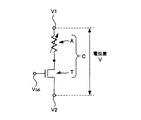
本実施の形態では、特に、この抵抗変化型記憶素子に対して、この記憶素子へのアクセスを制御する能動素子としてMISトランジスタを用いる。そして、図2に回路図を示すように、抵抗変化型記憶素子Aに対してMISトランジスタTを直列に接続して、記憶装置のメモリセルCを構成する。これにより、MISトランジスタTが、抵抗変化型記憶素子Aに対する負荷としても作用することになる。 In the present embodiment, in particular, for this resistance change type storage element, an MIS transistor is used as an active element for controlling access to the storage element. Then, as shown in a circuit diagram in FIG. 2, a MIS transistor T is connected in series to the resistance change storage element A to constitute a memory cell C of the storage device. As a result, the MIS transistor T also acts as a load for the resistance change storage element A.
即ち図2に示すように、抵抗変化型記憶素子AのMISトランジスタTに接続された端子とは反対側の端子に端子電圧V1が印加され、MISトランジスタTの抵抗変化型記憶素子Aに接続された端子とは反対側の一方(例えばソース側)の端子に端子電圧V2が印加され、MISトランジスタTのゲートにゲート電圧VGSが印加される構成となっている。
そして、メモリセルCを構成する抵抗変化型記憶素子A及びMISトランジスタTの両端にそれぞれ端子電圧V1,V2が印加されることにより、両端子間に電位差V(=|V2−V1|)を生じる。
That is, as shown in FIG. 2, the terminal voltage V1 is applied to the terminal opposite to the terminal connected to the MIS transistor T of the resistance change storage element A, and connected to the resistance change storage element A of the MIS transistor T. The terminal voltage V2 is applied to one terminal (for example, the source side) opposite to the terminal, and the gate voltage VGS is applied to the gate of the MIS transistor T.
Then, terminal voltages V1 and V2 are applied to both ends of the resistance change storage element A and the MIS transistor T constituting the memory cell C, respectively, thereby generating a potential difference V (= | V2−V1 |) between both terminals. .
なお、MISトランジスタTのオン抵抗値は、抵抗変化型記憶素子Aの高い抵抗値よりは低いことが望ましい。より望ましくは、抵抗変化型記憶素子Aの高い抵抗値の例えば数分の1以下として、充分低くなるようにする。
これは、MISトランジスタTのオン抵抗値が高いと、端子間に印加した電位差がほとんどMISトランジスタTにかかるため、電力がロスしてしまい、印加した電圧を効率良く記憶素子Aの抵抗の変化に使用することができないからである。
The on-resistance value of the MIS transistor T is preferably lower than the high resistance value of the resistance change storage element A. More desirably, the resistance value of the resistance change memory element A is set to a sufficiently low value, for example, less than a fraction of the high resistance value.
This is because when the on-resistance value of the MIS transistor T is high, the potential difference applied between the terminals is almost applied to the MIS transistor T, so that power is lost and the applied voltage is efficiently changed to the resistance of the memory element A. It is because it cannot be used.
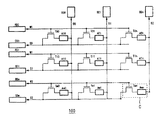
次に、本実施の形態の記憶装置の電気回路図を図3に示す。この電気回路図は、図2の各電圧(V1,V2,VGS)を印加するための電圧制御回路を含んでいる。 Next, FIG. 3 shows an electrical circuit diagram of the memory device of this embodiment. This electric circuit diagram includes a voltage control circuit for applying each voltage (V1, V2, VGS ) of FIG.
この記憶装置100は、(m+1)行・(n+1)列のメモリセルCが、マトリクス状に配置されて構成されている。メモリセルCは、図2に示したように、抵抗変化型記憶素子Aの一端がトランジスタTの一端(ここではドレイン)に接続されて構成されている。
トランジスタT(T00〜Tmn)のゲートは、ワード線W(W0〜Wm)に接続されている。抵抗変化型記憶素子Aの他端は、ビット線B(B0〜Bn)に接続されている。また、トランジスタTの他端(ソース)は、ソース線S(S0〜Sm)に接続されている。
さらに、ビット線B(B0〜Bn)は、その電圧制御回路であるビットデコーダBD(BD0〜BDn)に接続されている。ワード線W(W0〜Wm)は、その電圧制御回路であるロウデコーダRD(RD0〜RDm)に接続されている。ソース線S(S0〜Sm)は、その電圧制御回路であるソースデコーダSD(SD0〜SDm)に接続されている。
The
The gates of the transistors T (T00 to Tmn) are connected to the word lines W (W0 to Wm). The other end of the resistance change type storage element A is connected to the bit line B (B0 to Bn). The other end (source) of the transistor T is connected to the source line S (S0 to Sm).
Further, the bit lines B (B0 to Bn) are connected to a bit decoder BD (BD0 to BDn) which is a voltage control circuit thereof. The word lines W (W0 to Wm) are connected to row decoders RD (RD0 to RDm) which are voltage control circuits thereof. The source lines S (S0 to Sm) are connected to a source decoder SD (SD0 to SDm) that is a voltage control circuit thereof.
このように構成されている本実施の形態の記憶装置100では、例えば次のようにして、情報の記録を行うことができる。
情報の記録を行うべきメモリセルCに対応するワード線Wに対して、ロウデコーダRDによりゲート電圧VGSを印加して、MISトランジスタTのゲートをオンにする。そして、そのメモリセルCに対応するビット線B及びソース線Sに対して、ビットデコーダBD及びソースデコーダSDにより、図2に示した端子電圧V1,V2を印加する。これにより、メモリセルC内の抵抗変化型記憶素子A及びMISトランジスタTに、電圧Vを印加することができる。
In the
The gate voltage V GS is applied by the row decoder RD to the word line W corresponding to the memory cell C where information is to be recorded, and the gate of the MIS transistor T is turned on. Then, the terminal voltages V1 and V2 shown in FIG. 2 are applied to the bit line B and the source line S corresponding to the memory cell C by the bit decoder BD and the source decoder SD. Thereby, the voltage V can be applied to the resistance change storage element A and the MIS transistor T in the memory cell C.
このように電圧Vを印加したときに、抵抗変化型記憶素子Aの両端にかかる電圧が、前述した抵抗変化型記憶素子Aの書き込み閾値電圧よりも大きくなっていれば、抵抗変化型記憶素子Aの抵抗値が高抵抗の状態から低下して、低抵抗の状態へと遷移する。
これにより、抵抗変化型記憶素子Aへ情報の記録(以下、この場合を書き込みとする)を行うことができる。
また、抵抗変化型記憶素子Aの抵抗値が低抵抗の状態であるときに、MISトランジスタTのゲートをオンにすると共に、メモリセルC内の抵抗変化型記憶素子A及びMISトランジスタTに、書き込み時とは逆極性の電圧Vを印加すると、抵抗変化型記憶素子Aの両端にかかる電圧が、前述した抵抗変化型記憶素子Aの消去閾値電圧よりも大きくなっていれば、抵抗変化型記憶素子Aの抵抗値が低抵抗の状態から増大して、高抵抗の状態へと遷移する。
これにより、抵抗変化型記憶素子Aへ情報の記録(以下、この場合を消去とする)を行うことができる。
If the voltage applied to both ends of the resistance change storage element A when the voltage V is applied in this way is greater than the write threshold voltage of the resistance change storage element A described above, the resistance change storage element A The resistance value decreases from a high resistance state to a low resistance state.
Thereby, information can be recorded in the resistance change type storage element A (hereinafter, this case is referred to as writing).
Further, when the resistance value of the resistance change type storage element A is in a low resistance state, the gate of the MIS transistor T is turned on, and the resistance change type storage element A and the MIS transistor T in the memory cell C are written. When a voltage V having a polarity opposite to that of time is applied, if the voltage applied to both ends of the resistance change storage element A is larger than the erase threshold voltage of the resistance change storage element A, the resistance change storage element The resistance value of A increases from the low resistance state and transitions to the high resistance state.
As a result, information can be recorded (hereinafter referred to as erasure) in the resistance change storage element A.
なお、このとき、ワード線Wが各行のメモリセルCで共通になっているため、同一行の全てのメモリセルCにおいて、MISトランジスタTのゲートがオンになる。
従って、例えば同一行のメモリセルC群のうち一部のメモリセルCにだけ情報の記録を行う場合には、情報の記録を行わない他のメモリセルCについては、ビット線Bの電位を、ソース線Sの電位と同じ、又はソース線Sとの電位差が抵抗変化型記憶素子Aの閾値電圧(書き込み閾値電圧或いは消去閾値電圧)よりも充分小さくなるように設定して、記録が行われないようにする。
At this time, since the word line W is common to the memory cells C in each row, the gates of the MIS transistors T are turned on in all the memory cells C in the same row.
Therefore, for example, when information is recorded only in a part of the memory cells C in the memory cell C group in the same row, the potential of the bit line B is set for the other memory cells C that do not record information. Recording is not performed by setting the potential of the source line S to be the same as or different from the threshold voltage of the resistance change storage element A (write threshold voltage or erase threshold voltage). Like that.
次に、メモリセルCの両端に電圧を印加したときの変化について、その概略を説明する。
メモリセルCの両端に印加した電圧Vは、記憶素子AとMISトランジスタTとに分圧される。
このとき、前述したようにMISトランジスタTのオン抵抗値が記憶素子Aの高い抵抗値よりも充分低い構成であれば、記憶素子Aの抵抗値が高抵抗である状態では、印加した電圧のほとんどが記憶素子Aの両端に加わる。即ち、記憶素子Aの両端に加わる電圧VAについて、ほぼVA=Vとなる。
Next, an outline of a change when a voltage is applied to both ends of the memory cell C will be described.
The voltage V applied across the memory cell C is divided between the memory element A and the MIS transistor T.
At this time, if the ON resistance value of the MIS transistor T is sufficiently lower than the high resistance value of the memory element A as described above, most of the applied voltage is obtained in a state where the resistance value of the memory element A is high resistance. Is added to both ends of the memory element A. That is, the voltage VA applied across the storage element A is approximately VA = V.
ここで、記憶素子Aの閾値電圧Vthよりも印加電圧Vが大きい(V>Vth)場合には、記録動作が開始され、記憶素子Aの抵抗値R1が低下していく。この記憶素子Aの抵抗値R1の低下とともに、記憶素子Aの両端の電圧VAも減少していく。 Here, when the applied voltage V is larger than the threshold voltage Vth of the memory element A (V> Vth), the recording operation is started, and the resistance value R1 of the memory element A decreases. As the resistance value R1 of the storage element A decreases, the voltage VA across the storage element A also decreases.
やがて、記憶素子Aの両端の電圧VAがある電圧Vmin(≧Vth)まで減少すると、記憶素子Aの抵抗値R1の減少が止まり、それ以上は抵抗値R1が減少しなくなる。これにより、記憶素子Aの両端の電圧VAもVminで停止する。
これは、記憶素子Aの抵抗値R1の低下により記憶素子Aの両端の電圧VAが減少していくと、記憶素子Aに流れる電流Iと記憶素子Aの両端の電圧VAとの関係が、記憶素子AのI−V特性に近づいていき、この記憶素子AのI−V特性に達したときにそれ以上は変化できなくなるからである。即ち、記憶素子AのI−V特性に達した後に、記憶素子Aの抵抗値R1をさらに減少させるためには、今度は記憶素子Aの両端の電圧VAを増やす必要があるが、この電圧VAを増やすと記憶素子Aに流れる電流Iも増加し、記憶素子Aに直列接続されたMISトランジスタTにも同じ電流Iが流れるため、電流Iの増加に対応してMISトランジスタTの両端にかかる電圧(V−VA)も増加する。しかし、メモリセルCへの印加電圧Vが一定であり、各素子A,Tの両端にかかる電圧(VA,V−VA)はこの印加電圧Vを分圧しているので、両方を共に増やすことは不可能である。
このため、記憶素子AのI−V特性に達した状態で、記憶素子Aの抵抗値R1の低下が止まり、各素子A,Tの両端にかかる電圧(VA,V−VA)がそれぞれ一定値となる。
Eventually, when the voltage VA across the memory element A decreases to a certain voltage Vmin (≧ Vth), the resistance value R1 of the memory element A stops decreasing, and beyond that, the resistance value R1 does not decrease. As a result, the voltage VA across the memory element A also stops at Vmin.
This is because when the voltage VA across the memory element A decreases due to the decrease in the resistance value R1 of the memory element A, the relationship between the current I flowing through the memory element A and the voltage VA across the memory element A This is because the I-V characteristics of the element A are approached, and when the IV characteristics of the memory element A are reached, no further changes can be made. That is, after reaching the IV characteristic of the memory element A, in order to further reduce the resistance value R1 of the memory element A, it is necessary to increase the voltage VA across the memory element A this time. Is increased, the current I flowing through the storage element A also increases, and the same current I flows through the MIS transistor T connected in series to the storage element A. Therefore, the voltage applied to both ends of the MIS transistor T in response to the increase in the current I (V-VA) also increases. However, since the applied voltage V to the memory cell C is constant and the voltages (VA, V-VA) applied to both ends of the elements A and T divide the applied voltage V, it is impossible to increase both of them. Impossible.
For this reason, in the state where the IV characteristic of the memory element A is reached, the resistance value R1 of the memory element A stops decreasing, and the voltages (VA, V-VA) applied to both ends of the elements A and T are constant values. It becomes.
以下、この状態をこのメモリセルCの動作点と呼ぶ。本実施の形態の記憶装置100のメモリセルCでは、この動作点において、情報の記録動作(書き込み動作)が停止することになる。
この動作点における各素子A,Tの両端の電圧及びメモリセルCを流れる電流は、記憶素子AのI−V特性とMISトランジスタTのI−V特性とにより求めることができる。具体的には、例えば0側を起点として抵抗変化型記憶素子AのI−V特性(電圧−電流変化)を描き、例えばV側を起点としてMISトランジスタTのI−V特性(電圧−電流変化)を描き、これらのI−V特性(電圧−電流変化)の線の交点が動作点となる。なお、逆に0側を起点としてMISトランジスタTのI−V特性(電圧−電流変化)を描き、V側を起点として抵抗変化型記憶素子AのI−V特性(電圧−電流変化)を描いても、同様に動作点を求めることができる。
Hereinafter, this state is referred to as an operating point of the memory cell C. In the memory cell C of the
The voltage across the elements A and T and the current flowing through the memory cell C at this operating point can be obtained from the IV characteristics of the memory element A and the IV characteristics of the MIS transistor T. Specifically, for example, the IV characteristic (voltage-current change) of the resistance change type memory element A is drawn starting from the 0 side, and the IV characteristic (voltage-current change) of the MIS transistor T is drawn starting from the V side, for example. ), And the intersection of these IV characteristic (voltage-current change) lines is the operating point. Conversely, the IV characteristic (voltage-current change) of the MIS transistor T is drawn starting from the 0 side, and the IV characteristic (voltage-current change) of the resistance change memory element A is drawn starting from the V side. However, the operating point can be obtained similarly.
次に、印加電圧Vの極性を逆にして、情報の記録(消去)を行うときには、記憶素子Aの抵抗値が低いため、記憶素子Aの両端にかかる電圧VAが記憶素子Aの消去閾値電圧よりも大きくなるように印加電圧Vを設定する。
記憶素子Aの両端にかかる電圧VAが記憶素子Aの消去閾値電圧よりも大きければ、情報の記録(消去)が開始され、記憶素子Aの抵抗値が増大していく。記憶素子Aの抵抗値の増大に伴って記憶素子Aの分圧即ち記憶素子Aの両端にかかる電圧VAも増大するため、記憶素子Aの抵抗値の増大がさらに進行していく。記憶素子Aの抵抗値がある程度大きく(高抵抗に)なると、それ以上は抵抗値の増大が進行しなくなるため、ここで情報の記録動作(消去動作)が停止することになる。
この状態における各素子A,Tの両端の電圧及びメモリセルCを流れる電流も、上述の動作点と同様に、記憶素子AのI−V特性とMISトランジスタTのI−V特性とにより求めることができる。
Next, when recording (erasing) information with the polarity of the applied voltage V reversed, since the resistance value of the memory element A is low, the voltage VA applied across the memory element A is equal to the erase threshold voltage of the memory element A. The applied voltage V is set so as to be larger than that.
If the voltage VA applied across the memory element A is larger than the erase threshold voltage of the memory element A, information recording (erasing) is started and the resistance value of the memory element A increases. As the resistance value of the memory element A increases, the partial pressure of the memory element A, that is, the voltage VA applied to both ends of the memory element A also increases, so that the resistance value of the memory element A further increases. When the resistance value of the memory element A becomes large to some extent (high resistance), the resistance value does not increase any further, and the information recording operation (erasing operation) is stopped here.
In this state, the voltages across the elements A and T and the current flowing through the memory cell C are also obtained from the IV characteristics of the memory element A and the IV characteristics of the MIS transistor T, as in the above-described operating point. Can do.
このようにメモリセルCの両端に電圧Vを印加することにより、そのメモリセルCの記憶素子Aに情報の記録、即ち書き込みや消去を行うことができる。 Thus, by applying the voltage V to both ends of the memory cell C, information can be recorded on the memory element A of the memory cell C, that is, writing or erasing can be performed.
上述した情報の記録についての説明では、記憶素子Aの抵抗値が高い状態と低い状態の2つの状態を利用して情報の記録を行うようにしているため、例えばデータ“0”とデータ“1”といった、2値(1ビット)の情報の記録を行うことができる。
本実施の形態の記憶装置では、さらにこれを応用して、3値や4値(2ビット)以上の多値記録を行うものである。
以下、本実施の形態における多値記録について説明する。
In the description of the information recording described above, since information recording is performed using two states of the storage element A having a high resistance value and a low resistance value, for example, data “0” and data “1” are recorded. Binary information (1 bit) can be recorded.
In the storage device of the present embodiment, this is further applied to perform multi-value recording of three values or four values (2 bits) or more.
Hereinafter, multilevel recording in the present embodiment will be described.
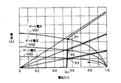
MISトランジスタTは、ゲートに印加されるゲート電圧VGSの大きさによって、オン抵抗が変化し、I−V特性も変化する。
そこで、メモリセルCのMISトランジスタTのゲート電圧VGSを変更することにより、MISトランジスタTのI−V特性を変化させて、これにより動作点の位置を変えることが可能になる。
In the MIS transistor T, the on-resistance changes depending on the magnitude of the gate voltage V GS applied to the gate, and the IV characteristic also changes.
Therefore, by changing the gate voltage V GS of the MIS transistor T of the memory cell C, it is possible to change the IV characteristic of the MIS transistor T, thereby changing the position of the operating point.
即ち、図4に示すように、MISトランジスタTのゲート電圧VGSを、VG1,VG2,VG3(VG1>VG2>VG3)と変えることにより、MISトランジスタTのI−V特性が変化する。MISトランジスタTのゲート電圧VGSが大きいほど、電流がよく流れ、オン抵抗が低くなることから、I−V特性の曲線が図4中で上方になる。
そして、MISトランジスタTのゲート電圧VGSを、VG1,VG2,VG3と変えることにより、動作点もそれぞれP1,P2,P3と異なる点になり、動作点における記憶素子Aの抵抗値も異なることになる。
That is, as shown in FIG. 4, the IV characteristic of the MIS transistor T is changed by changing the gate voltage V GS of the MIS transistor T to VG1, VG2, and VG3 (VG1>VG2> VG3). The larger the gate voltage V GS of the MIS transistor T, the more current flows and the lower the on-resistance. Therefore, the curve of the IV characteristic is upward in FIG.
Then, by changing the gate voltage V GS of the MIS transistor T to VG1, VG2, and VG3, the operating point is also different from P1, P2, and P3, respectively, and the resistance value of the memory element A at the operating point is also different. Become.
そして、例えば、各動作点P1,P2,P3を、それぞれ2ビット情報の“11”,“10”,“01”に割り当て、高い抵抗値の状態(書き込み前及び消去後)を“00”に割り当てることにより、記憶素子Aに2ビット情報を記憶させることが可能になる。 Then, for example, each operating point P1, P2, P3 is assigned to “11”, “10”, “01” of 2-bit information, respectively, and the state of high resistance value (before writing and after erasing) is set to “00”. By assigning, 2-bit information can be stored in the storage element A.
このように、書き込みを行った素子の抵抗値に対して、複数のビット情報を割り当てることにより、多値記録を実現することができる。 As described above, multi-value recording can be realized by assigning a plurality of pieces of bit information to the resistance value of the element to which writing has been performed.
なお、実際の記憶装置では、メモリセルC毎のMISトランジスタTに若干の特性の違いが存在することがあるため、このことを考慮して、図4に示した動作点P1,P2,P3だけでなく、動作点P1,P2,P3付近のある程度幅のある範囲(記憶素子Aの抵抗値の範囲)を、それぞれの情報(例えば、“01”,“10”,“11”の各データ)に割り当てる。 In an actual memory device, there may be a slight characteristic difference in the MIS transistor T for each memory cell C. Therefore, only the operating points P1, P2, and P3 shown in FIG. In addition, a range having a certain width in the vicinity of the operating points P1, P2, and P3 (resistance value range of the storage element A) is represented by each piece of information (for example, “01”, “10”, and “11” data). Assign to.
例えば、記憶素子Aの抵抗値が、3kΩ以下である場合を2ビット情報の“11”、3kΩ〜6kΩである場合を“10”、6kΩ〜9kΩである場合を“01”、9kΩ以上である場合を“00”、といったように割り当てる。 For example, when the resistance value of the memory element A is 3 kΩ or less, “11” of 2-bit information is “10”, when it is 3 kΩ to 6 kΩ, “01” when it is 6 kΩ to 9 kΩ, and “01” is 9 kΩ or more. The case is assigned as “00”.
同様にして、さらに細かく抵抗値の範囲を区切ることにより、3ビット情報(8値)、4ビット情報(16値)も記録することが可能である。 Similarly, 3-bit information (8 values) and 4-bit information (16 values) can be recorded by further dividing the resistance value range.
上述のように多値記録を行った記憶素子Aに記録された情報を読み出す場合には、読み出し用の電流をメモリセルCに流して、この電流が記憶素子Aの抵抗値に比例して流れるため、記憶素子Aの抵抗値を検出して、情報の内容を検出することができる。 When reading the information recorded in the storage element A that has been subjected to multi-value recording as described above, a read current is supplied to the memory cell C, and this current flows in proportion to the resistance value of the storage element A. Therefore, the content of information can be detected by detecting the resistance value of the memory element A.
ただし、この読み出し時において、記憶素子Aの抵抗値を低下させないようにする必要がある。
そのために、読み出し時において、MISトランジスタTのゲートに、比較的高い電圧、例えば電源電圧VDDを印加する。これにより、MISトランジスタTのオン抵抗が小さくなるため、読み出し用の電流を流したときに記憶素子Aの両端にかかる電圧VAが小さくなり、記憶素子Aの抵抗値を低下させてしまうことがない。
この他に、例えば、読み出し時において、メモリセルCの両端への印加電圧をその情報の記録に対応する動作点の書き込み時のメモリセルCの両端への印加電圧よりも小さくすることも考えられるが、上述のようにゲート電圧に電源電圧を印加する方法が電圧を制御しやすい点で優れている。
However, it is necessary to prevent the resistance value of the memory element A from being lowered during the reading.
Therefore, at the time of reading, a relatively high voltage, for example, the power supply voltage V DD is applied to the gate of the MIS transistor T. As a result, the on-resistance of the MIS transistor T is reduced, so that the voltage VA applied to both ends of the memory element A when the read current is supplied is reduced, and the resistance value of the memory element A is not reduced. .
In addition, for example, at the time of reading, it is conceivable that the voltage applied to both ends of the memory cell C is made smaller than the voltage applied to both ends of the memory cell C at the time of writing the operating point corresponding to the recording of the information. However, the method of applying the power supply voltage to the gate voltage as described above is excellent in that the voltage can be easily controlled.
また、記憶素子Aを低抵抗の状態から高抵抗の状態に遷移させるとき、即ち消去を行うときにも、MISトランジスタTのゲート電圧VGSを、比較的高い電圧、例えば電源電圧VDDにすることが望ましい。これにより、MISトランジスタTのオン抵抗が小さくなるため、メモリセルCの両端への印加電圧Vを大きくしなくても、記憶素子Aの両端にかかる電圧VAを消去閾値以上に大きくすることが可能になる。
従って、比較的小さい印加電圧Vで消去を行うことが可能になるため、消去に必要となるメモリセルCへの印加電圧Vを低減して、配線や素子にかかる負担を低減することができる。
Further, when the memory element A is changed from the low resistance state to the high resistance state, that is, when erasing is performed, the gate voltage V GS of the MIS transistor T is set to a relatively high voltage, for example, the power supply voltage V DD . It is desirable. As a result, the on-resistance of the MIS transistor T is reduced, so that the voltage VA applied to both ends of the memory element A can be made larger than the erase threshold without increasing the applied voltage V to both ends of the memory cell C. become.
Accordingly, since erasing can be performed with a relatively small applied voltage V, the applied voltage V to the memory cell C required for erasing can be reduced, and the burden on wiring and elements can be reduced.
なお、図5に示すように、メモリセルCの両端に印加する電圧Vを変更しても、同様に動作点を異ならせることができるため、これにより多値記録を行うことが可能である。
図5では、メモリセルCの両端に印加する電圧Vを、2.0V,1.0V,0.65Vと変更することにより、動作点をP1,P2,P3と異ならせている。
Note that, as shown in FIG. 5, even if the voltage V applied to both ends of the memory cell C is changed, the operating point can be similarly changed, so that multi-value recording can be performed.
In FIG. 5, the operating point is made different from P1, P2, and P3 by changing the voltage V applied across the memory cell C to 2.0V, 1.0V, and 0.65V.
また、MISトランジスタTのゲート電圧VGSと、メモリセルCの両端に印加する電圧Vとを、両方とも変更してもよい。
このようにしても、多値記録を行うことが可能である。この構成は、例えばメモリセルCの両端に印加する印加電圧Vを大きく(幅広く)変化させることが難しい場合に好適である。
Further, both the gate voltage V GS of the MIS transistor T and the voltage V applied to both ends of the memory cell C may be changed.
Even in this way, multi-value recording can be performed. This configuration is suitable, for example, when it is difficult to change the applied voltage V applied to both ends of the memory cell C greatly (widely).
なお、本実施の形態では、記憶素子Aが図1に示したI−V特性を有するため、記憶素子Aの抵抗値を低くする方向では、ゲート電圧VGSやメモリセルCへの印加電圧Vを変化させることにより、記憶素子Aの抵抗値が低くなるため、図4のP2からP1へ遷移させるというように、動作点同士で直接遷移させることが可能である。 In this embodiment, since the memory element A has the IV characteristics shown in FIG. 1, the gate voltage V GS and the applied voltage V to the memory cell C are reduced in the direction of decreasing the resistance value of the memory element A. Since the resistance value of the memory element A is lowered by changing the value, it is possible to make a direct transition between operating points, such as a transition from P2 to P1 in FIG.
一方、記憶素子Aの抵抗値を高くする方向(例えば図4のP1からP2への遷移)では、ゲート電圧VGSやメモリセルCへの印加電圧Vを変化させても、記憶素子Aの抵抗値が高くならないため、動作点同士で直接遷移させることができない。
そこで、一旦逆極性の電圧を印加して低抵抗の状態(オーミック特性)から高抵抗の状態へ遷移させ、その後に改めて所望の抵抗値に遷移させる。この場合には、2段階の遷移が必要になるが、それでもパルスの回数によって抵抗値を規定する構成の記憶装置と比較すると、充分に短い時間で情報の記録を行うことができる。
On the other hand, in the direction in which the resistance value of the memory element A is increased (for example, transition from P1 to P2 in FIG. 4), the resistance of the memory element A can be changed even when the gate voltage VGS or the applied voltage V to the memory cell C is changed. Since the value does not increase, it is not possible to make a direct transition between operating points.
Therefore, a voltage having a reverse polarity is applied once to make a transition from a low resistance state (ohmic characteristic) to a high resistance state, and then to a desired resistance value again. In this case, two-stage transition is required, but even so, information can be recorded in a sufficiently short time as compared with a storage device having a resistance value defined by the number of pulses.
ただし、動作点P1,P2,P3にそれぞれ対応する3つの抵抗値(以下、「書き込みレベル」とする)から、消去後の抵抗値(以下、「消去レベル」とする)に至るまでの経路は3種類存在しており、前述したように、それぞれの持つ消去特性(抵抗値、抵抗値のばらつき、記録した情報の保持特性等)は異なっている。
そこで、本実施の形態では、各経路の消去特性の不一致を解消するために、メモリセルを構成している抵抗変化型記憶素子に対するオーバーライトが可能であることに着目して、消去レベルに変化させる際に、常に最も抵抗値の低い書き込みレベルを経由させる。
即ち、抵抗値の高低が、書き込みレベル1(動作点P1)<書き込みレベル2(動作点P2)<書き込みレベル3(動作点P3)<消去レベル、の関係にあるとき、消去レベルに変化させる際に、常に書き込みレベル1(動作点P1)を経由させる。
例えば、書き込みレベル2(動作点P2)→消去レベルとする際には、書き込みレベル2(動作点P2)→書き込みレベル1(動作点P1)→消去レベルとする。
However, the path from the three resistance values (hereinafter referred to as “write level”) corresponding to the operating points P1, P2 and P3 to the resistance value after erasure (hereinafter referred to as “erase level”) is There are three types, and as described above, the erasing characteristics (resistance value, variation in resistance value, retention characteristic of recorded information, etc.) are different.
Therefore, in this embodiment, in order to eliminate the mismatch of the erase characteristics of the respective paths, paying attention to the fact that the resistance change type storage element constituting the memory cell can be overwritten, the erase level is changed. When writing, always use the write level with the lowest resistance value.
That is, when the resistance value is in the relationship of write level 1 (operation point P1) <write level 2 (operation point P2) <write level 3 (operation point P3) <erase level, when changing to the erase level In addition, the write level 1 (operating point P1) is always passed.
For example, when writing level 2 (operating point P2) → erasing level, writing level 2 (operating point P2) → writing level 1 (operating point P1) → erasing level is set.
これにより、記憶素子Aの抵抗値を高くする方向に変える場合、即ち例えば、書き込みレベル2(動作点P2)から書き込みレベル3(動作点P3)へ変えるためには、書き込みレベル2(動作点P2)→書き込みレベル1(動作点P1)→消去レベル→書き込みレベル3(動作点P3)と、3段階の遷移を実行することになる。 Thereby, when changing the resistance value of the memory element A in the direction of increasing, that is, for example, to change from the write level 2 (operating point P2) to the write level 3 (operating point P3), the write level 2 (operating point P2). ) → write level 1 (operating point P1) → erase level → write level 3 (operating point P3).
上述のように、消去レベルに変化させる際に、常に最も抵抗値の低い書き込みレベルを経由させることにより、経路の消去特性が一定となるので、消去レベルをほぼ一定にして消去レベルのばらつきを大幅に低減することができる。 As described above, when changing to the erasure level, the erasure characteristic of the path is made constant by always passing through the write level having the lowest resistance value. Can be reduced.
本実施の形態の記憶装置100では、抵抗変化型記憶素子AとMISトランジスタTとを直列に接続してメモリセルCを構成し、MISトランジスタTのゲート電圧VGSやメモリセルCの両端への印加電圧Vを変更することにより、動作点を変えて記憶素子Aの情報の記録(書き込みや消去)後の抵抗値を複数のレベル(点もしくは範囲)に制御して、記憶素子Aに3値以上の情報の記録、即ち多値記録を行うことができる。
In the
そして、本実施の形態の記憶装置では、MISトランジスタTのゲート電圧VGSやメモリセルCの両端への印加電圧Vを変更するだけで、情報の記録後の記憶素子Aの抵抗値を変更することができるため、多値記録を行う場合でも、1クロックの電圧パルス・電流パルスで済み、パルス幅の制御や多数回のパルスが必要なくなる。
これにより、短い時間で多値記録を行うことが可能である。
In the memory device according to the present embodiment, the resistance value of the memory element A after recording information is changed only by changing the gate voltage V GS of the MIS transistor T and the voltage V applied to both ends of the memory cell C. Therefore, even when performing multi-value recording, only one voltage pulse / current pulse is required, and pulse width control and multiple pulses are not required.
Thereby, multi-value recording can be performed in a short time.
また、本実施の形態の記憶装置では、メモリセルCの選択を行うためにメモリセルC内に設けられているアクセス用のMISトランジスタTを、メモリセルCの動作点を制御するための回路素子として利用しているため、メモリセルC内にさらに回路素子を追加しなくても、多値情報を記録することが可能である。
即ち、本実施の形態の記憶装置では、簡素な構成により、多値記録を行うことが可能である。
In the memory device of the present embodiment, the MIS transistor T for access provided in the memory cell C for selecting the memory cell C is used as a circuit element for controlling the operating point of the memory cell C. Therefore, multi-value information can be recorded without adding further circuit elements in the memory cell C.
That is, the storage device of this embodiment can perform multi-value recording with a simple configuration.
さらに、本実施の形態の記憶装置では、図3に示したように、各行のメモリセルCのMISトランジスタTのゲートに共通のワード線Wが接続され、このワード線WがロウデコーダRDに接続されている。
このため、このロウデコーダRDにワード線Wの電位制御を行う回路を接続するか、ロウデコーダRD内にワード線Wの電位制御を行う回路を内蔵することにより、簡素な構成でメモリセルCのMISトランジスタTのゲート電圧VGSを制御することができる。
そして、前述したように、メモリセルCのMISトランジスタTのゲート電圧VGSを変更することによって、MISトランジスタTのI−V特性及びオン抵抗を変化させて、これにより動作点を変更することができることから、多値記録を行うことができる。
即ち、本実施の形態の記憶装置では、簡素な構成により、メモリセルCのMISトランジスタTのゲート電圧VGSを制御して、多値記録を行うことが可能である。
Furthermore, in the memory device of the present embodiment, as shown in FIG. 3, a common word line W is connected to the gates of the MIS transistors T of the memory cells C in each row, and this word line W is connected to the row decoder RD. Has been.
Therefore, by connecting a circuit for controlling the potential of the word line W to the row decoder RD, or by incorporating a circuit for controlling the potential of the word line W in the row decoder RD, the memory cell C can be configured with a simple configuration. The gate voltage V GS of the MIS transistor T can be controlled.
As described above, by changing the gate voltage V GS of the MIS transistor T of the memory cell C, the IV characteristic and the on-resistance of the MIS transistor T can be changed, thereby changing the operating point. Therefore, multi-value recording can be performed.
That is, in the memory device of this embodiment, multi-value recording can be performed by controlling the gate voltage V GS of the MIS transistor T of the memory cell C with a simple configuration.
また、このようにロウデコーダRDに対してワード線Wの電位制御を行う回路を設けることにより、ワード線Wの電位を一定とすることによって、同一行のメモリセルに対して一括して読み出しを行うことが可能になる。 In addition, by providing a circuit for controlling the potential of the word line W in the row decoder RD as described above, by making the potential of the word line W constant, the memory cells in the same row can be read collectively. It becomes possible to do.
また、図5に示したように、メモリセルCの両端に印加する電圧Vを変更するには、例えば、図6Aに電気回路図を示すように、ビットデコーダBD0にデコーダ抵抗制御信号SDR0を供給するように構成し、このデコーダ抵抗制御信号SDR0により、ビットデコーダBD0内の可変抵抗素子R0又はスイッチング素子の抵抗値を制御すればよい。このビットデコーダBD0内の可変抵抗素子R0又はスイッチング素子も、MISトランジスタT00と同じく、記憶素子A00に対する負荷抵抗となるものである。
そして、ビットデコーダBD0は、通常可変抵抗素子R0又はスイッチング素子を内部に備えているため、新たな構成を追加しなくても簡易な構成で、メモリセルCの両端に印加する電圧Vを変更することができる。
なお、行方向のメモリセルCに共通に接続されたソース線Sから特定のソース線Sを選択するソースデコーダSDに対して、ソース線Sの電位制御を行う回路を設けたり、ソースデコーダSD内の可変抵抗素子又はスイッチング素子の抵抗値を制御したりしても、同様にメモリセルCの両端に印加する電圧Vを制御することが可能である。
Further, as shown in FIG. 5, in order to change the voltage V applied to both ends of the memory cell C, for example, as shown in the electric circuit diagram of FIG. 6A, the decoder resistance control signal SDR0 is supplied to the bit decoder BD0. The resistance value of the variable resistance element R0 or the switching element in the bit decoder BD0 may be controlled by the decoder resistance control signal SDR0. Similarly to the MIS transistor T00, the variable resistance element R0 or the switching element in the bit decoder BD0 also serves as a load resistance for the storage element A00.
Since the bit decoder BD0 normally includes the variable resistance element R0 or the switching element therein, the voltage V applied to both ends of the memory cell C is changed with a simple configuration without adding a new configuration. be able to.
A circuit for controlling the potential of the source line S is provided for the source decoder SD that selects a specific source line S from the source lines S commonly connected to the memory cells C in the row direction. It is possible to control the voltage V applied to both ends of the memory cell C in the same manner even when the resistance value of the variable resistance element or the switching element is controlled.
また、MISトランジスタTのゲート電圧VGSと、メモリセルCの両端に印加する電圧Vとを、両方とも変更する場合には、例えば、図6Bに電気回路図を示すように、図6Aの場合と同様にビットデコーダBD0にデコーダ抵抗制御信号SDR0を供給すると共に、例えば、ロウデコーダRD0に接続されたワード線W0の電位制御を行う回路(図示せず)から、ワード線W0の電位を制御する信号SW0をロウデコーダRD0に供給して、MISトランジスタTのゲート電圧VGSを制御するように構成すればよい。或いは、ロウデコーダRD0に、ワード線W0の電位制御を行う回路を内蔵させてもよい。
なお、図6A及び図6Bの各電気回路図では、図面を簡略化にするために、1つのメモリセルについて示しているが、他の行や他の列のメモリセルも同様に構成される。
Further, when both the gate voltage V GS of the MIS transistor T and the voltage V applied to both ends of the memory cell C are changed, for example, as shown in the electric circuit diagram of FIG. Similarly to the above, the decoder resistance control signal SDR0 is supplied to the bit decoder BD0 and, for example, the potential of the word line W0 is controlled from a circuit (not shown) that controls the potential of the word line W0 connected to the row decoder RD0. provides signals SW0 to the row decoder RD0, it may be configured to control the gate voltage V GS of the MIS transistor T. Alternatively, a circuit for controlling the potential of the word line W0 may be incorporated in the row decoder RD0.
In each electric circuit diagram of FIGS. 6A and 6B, one memory cell is shown for simplification of the drawing, but memory cells in other rows and other columns are similarly configured.
従って、本実施の形態によれば、簡素な構成であり、かつ多値記録を行うことが可能である記憶装置を実現することができる。 Therefore, according to the present embodiment, it is possible to realize a storage device having a simple configuration and capable of performing multi-value recording.
さらに、本実施の形態の記憶装置100によれば、消去レベルに変化させる際には、即ち消去の動作を行う際には、常に最も抵抗値の低い書き込みレベルを経由させることにより、消去の経路の消去特性が一定となるので、消去レベルをほぼ一定にして、消去レベルのばらつきを大幅に低減することができる。
これにより、消去の動作や情報の読み出し動作を安定して行うことができるので、安定して動作する信頼性の高い記憶装置100を実現することができる。
Furthermore, according to the
Accordingly, an erasing operation and an information reading operation can be stably performed, and thus a highly
ここで、多値記録を行う記憶装置において、一旦最低書き込みレベルを経由した方が、消去特性が良好であることを、具体例を用いて示す。
図2に回路構成を示すメモリセルCを多数有して成る記憶装置を、実際に作製し、書き込み・消去を繰り返し行った。
トランジスタTのゲート電圧VGSを一定の値として、書き込み・消去を106(100万)回繰り返した後において、多数ある各メモリセルCの記憶素子について書き込み後の抵抗値と消去後の抵抗値とを測定した。この測定を、書き込み時のトランジスタTのゲート電圧VGSを0.7V,0.9V,1.5Vの3通りで変えて、それぞれ行った。VGS=0.7Vのときの書き込みレベルを「書き込みレベル3」、VGS=0.9Vのときの書き込みレベルを「書き込みレベル2」、VGS=1.5Vのときの書き込みレベルを「書き込みレベル1」として、3つの書き込みレベルを設定した。各レベルの抵抗値の関係は、書き込みレベル1<書き込みレベル2<書き込みレベル3<消去レベルである。なお、消去時のトランジスタTのゲート電圧VGSは、いずれの場合も電源電圧と同じ1.8Vとした。
記憶素子の書き込み後の抵抗値の分布と消去後の抵抗値の分布を、それぞれ図7と図8に示す。図7及び図8において、横軸は書き込み及び消去のそれぞれの抵抗値、縦軸は累積確率分布[%]である。折れ線が縦に立っているほど、抵抗値のばらつきが小さいことを表している。
3つの線のうち、実線は、繰り返し書き込み・消去の各回で、書き込みレベル3と消去レベルとに変化させた場合を示している。点線は、書き込みレベル2と消去レベルとに変化させた場合を示している。破線は、書き込みレベル1と消去レベルとに変化させた場合を示している。このうち、破線は、最も抵抗値の低い書き込みレベル1から消去を行った場合である。他の2つの線は、最低書き込みレベル(書き込みレベル1)を経由しない場合に相当する。
Here, in a storage device that performs multi-value recording, it will be shown by using a specific example that the erasing characteristics are better once passing through the lowest write level.
A memory device having a large number of memory cells C whose circuit configuration is shown in FIG. 2 was actually fabricated, and writing / erasing was repeated.
The resistance value after writing and the resistance value after erasing the memory element of each of the many memory cells C after the writing / erasing is repeated 10 6 (1 million) times with the gate voltage V GS of the transistor T being a constant value. And measured. This measurement was performed by changing the gate voltage V GS of the transistor T at the time of writing in three ways of 0.7V, 0.9V, and 1.5V. The write level when V GS = 0.7 V is “
The distribution of resistance values after writing and the distribution of resistance values after erasing are shown in FIGS. 7 and 8, respectively. In FIGS. 7 and 8, the horizontal axis represents the resistance value for writing and erasing, and the vertical axis represents the cumulative probability distribution [%]. The more the line is standing vertically, the smaller the variation in resistance value.
Of the three lines, the solid line shows the case where the writing level is changed to the erasing level at each time of repeated writing / erasing. A dotted line indicates a case where the level is changed between the
図7からわかるように、最も低い書き込みレベル1では、10万回の繰り返し後も抵抗値のばらつきがほとんどない。これに対して、書き込みレベル3では、11kΩ〜14.5kΩまでの抵抗値の分布がある。
図8からわかるように、最も低い書き込みレベル1から消去した場合が、消去レベルのバラツキが小さい。ばらつきが約二桁も改善されている。
即ち、多値記録を行う場合においても、例えば、書き込みレベル2から直接消去レベルに変化させるのではなく、一旦最も低い書き込みレベル1までオーバーライトを行った後に消去を行うのが、最も良いことがわかる。
As can be seen from FIG. 7, at the
As can be seen from FIG. 8, when the erase is performed from the
That is, even when performing multi-level recording, for example, it is best not to directly change from the
なお、この例ではゲート電圧VGS=1.5Vとした場合が最低書き込みレベル(書き込みレベル1)となっているが、常にVGS=1.5Vが最低書き込みレベルになるとは限らない。例えば、ゲート電圧VGS=2.0Vとした場合に、最低書き込みレベルとなることもある。 In this example, the gate voltage V GS = 1.5V is the lowest write level (write level 1), but V GS = 1.5V is not always the lowest write level. For example, when the gate voltage V GS = 2.0 V, the minimum write level may be reached.
上述の実施の形態では、MISトランジスタTを記憶素子Aに直列に接続してメモリセルCを構成していたが、記憶素子に直列に接続する回路素子は、MISトランジスタに限定されるものではない。
記憶素子に直列に接続する回路素子として、例えばバイポーラトランジスタを用いることも可能である。その場合も、バイポーラトランジスタのベース電流又はメモリセルの両端への印加電圧を変更することにより、多値記録を行うことが可能である。
さらに、記憶素子に直列に接続する回路素子として、例えばダイオード等の能動素子や抵抗素子を使用することも可能である。
これらダイオードや抵抗素子を使用した場合には、メモリセルの両端に印加する電圧を変更することによって、多値記録を行うことが可能になる。
なお、トランジスタやダイオード等の能動素子を記憶素子に直列に接続する回路素子として用いた場合には、メモリセルの選択を能動素子で行うことが可能になる。
In the above-described embodiment, the memory cell C is configured by connecting the MIS transistor T in series with the storage element A. However, the circuit element connected in series with the storage element is not limited to the MIS transistor. .
For example, a bipolar transistor can be used as the circuit element connected in series to the memory element. Even in that case, it is possible to perform multi-value recording by changing the base current of the bipolar transistor or the voltage applied to both ends of the memory cell.
Further, as a circuit element connected in series to the memory element, for example, an active element such as a diode or a resistance element can be used.
When these diodes and resistance elements are used, multi-value recording can be performed by changing the voltage applied to both ends of the memory cell.
Note that when an active element such as a transistor or a diode is used as a circuit element connected in series to a memory element, the memory cell can be selected by the active element.
上述の実施の形態では、記憶素子Aが図1に示したI−V特性を有する構成であったが、本発明では、メモリセルを構成する記憶素子の構成は、図1に示したI−V特性と同様の傾向の特性を有する記憶素子に限らず、抵抗変化型記憶素子一般に広く適用することが可能である。 In the above-described embodiment, the storage element A has the configuration having the IV characteristics shown in FIG. 1, but in the present invention, the configuration of the storage element that constitutes the memory cell is the same as that shown in FIG. The present invention is not limited to memory elements having the same tendency as the V characteristics, and can be widely applied to resistance change memory elements in general.
本発明は、上述の実施の形態に限定されるものではなく、本発明の要旨を逸脱しない範囲でその他様々な構成が取り得る。 The present invention is not limited to the above-described embodiment, and various other configurations can be taken without departing from the gist of the present invention.
C メモリセル、100 記憶装置、A (抵抗変化型)記憶素子、T MISトランジスタ、VGS ゲート電圧 C memory cell, 100 memory device, A (resistance change type) memory element, T MIS transistor, V GS gate voltage
Claims (5)
前記記憶素子は、2つの電極の間に記憶層が挟まれてなり、前記記憶層にはCu,Ag,Znのうち少なくともいずれか1つの金属元素を含有しており、
前記記憶素子の抵抗値が高い状態から抵抗値が低い状態へ変化させる動作を書き込みと定義し、前記記憶素子の抵抗値が低い状態から抵抗値が高い状態へ変化させる動作を消去と定義したとき、
前記書き込みの動作と、前記消去の動作とでは、前記記憶素子に印加される電圧の方向が逆であり、
前記書き込みの際に、前記回路素子又は前記記憶素子に印加される電圧又は電流を制御することにより、前記書き込み後の前記記憶素子の抵抗値が、異なる複数のレベルに設定され、
前記記憶素子は、抵抗値が低い状態の前記複数のレベル及び前記消去後の抵抗値が高い状態に、それぞれ異なる情報が割り当てられ、各前記メモリセルの前記記憶素子に対して、それぞれ3値以上の情報を記憶することが可能であり、
抵抗値が低い状態の前記複数のレベルのうち、最も抵抗値の低いレベル以外のレベルから消去する際には、前記最も抵抗値の低いレベルへ変化させる過程が行われてから、前記抵抗値が高い状態に変化させる過程が行われる
記憶装置。 A memory cell includes a memory element that stores and holds information according to a state of electrical resistance, and a circuit element that is connected in series with the memory element and serves as a load.
The memory element includes a memory layer sandwiched between two electrodes, and the memory layer contains at least one metal element of Cu, Ag, and Zn,
When the operation of changing the resistance value of the memory element from a high resistance value to a low resistance value is defined as writing, and the operation of changing the memory element resistance value from a low resistance value to a high resistance value is defined as erasing. ,
In the write operation and the erase operation, the direction of the voltage applied to the memory element is opposite,
At the time of writing, by controlling the voltage or current applied to the circuit element or the memory element, the resistance value of the memory element after the writing is set to a plurality of different levels,
The memory element is assigned different information to the plurality of levels having a low resistance value and a state having a high resistance value after erasure, and each of the memory elements of each memory cell has three or more values. It is possible to memorize the information of
When erasing from a level other than the lowest resistance value among the plurality of levels having a low resistance value, a process of changing to the lowest resistance value is performed, and then the resistance value is changed. A storage device that undergoes a process of changing to a high state.
Priority Applications (2)
| Application Number | Priority Date | Filing Date | Title |
|---|---|---|---|
| JP2006158868A JP4297136B2 (en) | 2006-06-07 | 2006-06-07 | Storage device |
| US11/757,107 US7715220B2 (en) | 2006-06-07 | 2007-06-01 | Memory apparatus |
Applications Claiming Priority (1)
| Application Number | Priority Date | Filing Date | Title |
|---|---|---|---|
| JP2006158868A JP4297136B2 (en) | 2006-06-07 | 2006-06-07 | Storage device |
Publications (2)
| Publication Number | Publication Date |
|---|---|
| JP2007328857A JP2007328857A (en) | 2007-12-20 |
| JP4297136B2 true JP4297136B2 (en) | 2009-07-15 |
Family
ID=38861366
Family Applications (1)
| Application Number | Title | Priority Date | Filing Date |
|---|---|---|---|
| JP2006158868A Expired - Fee Related JP4297136B2 (en) | 2006-06-07 | 2006-06-07 | Storage device |
Country Status (2)
| Country | Link |
|---|---|
| US (1) | US7715220B2 (en) |
| JP (1) | JP4297136B2 (en) |
Families Citing this family (64)
| Publication number | Priority date | Publication date | Assignee | Title |
|---|---|---|---|---|
| WO2008122919A1 (en) * | 2007-04-05 | 2008-10-16 | Nxp B.V. | A memory cell, a memory array and a method of programming a memory cell |
| JP2009099206A (en) * | 2007-10-17 | 2009-05-07 | Toshiba Corp | Resistance change memory device |
| JP5050813B2 (en) * | 2007-11-29 | 2012-10-17 | ソニー株式会社 | Memory cell |
| JP5171955B2 (en) | 2008-08-29 | 2013-03-27 | 株式会社東芝 | Multi-value resistance change memory |
| JP5272596B2 (en) * | 2008-09-09 | 2013-08-28 | 日本電気株式会社 | Storage device and control method thereof |
| KR20110080153A (en) * | 2008-10-08 | 2011-07-12 | 더 리젠츠 오브 더 유니버시티 오브 미시건 | Silicon-based nanoscale resistive device with adjustable resistance |
| US8071972B2 (en) | 2008-10-20 | 2011-12-06 | The Regents Of The University Of Michigan | Silicon based nanoscale crossbar memory |
| KR101519363B1 (en) | 2009-02-16 | 2015-05-13 | 삼성전자 주식회사 | Multi-level nonvolatile memory device using variable resistive element |
| US9601692B1 (en) | 2010-07-13 | 2017-03-21 | Crossbar, Inc. | Hetero-switching layer in a RRAM device and method |
| US8946046B1 (en) | 2012-05-02 | 2015-02-03 | Crossbar, Inc. | Guided path for forming a conductive filament in RRAM |
| US9570678B1 (en) | 2010-06-08 | 2017-02-14 | Crossbar, Inc. | Resistive RAM with preferental filament formation region and methods |
| US9012307B2 (en) | 2010-07-13 | 2015-04-21 | Crossbar, Inc. | Two terminal resistive switching device structure and method of fabricating |
| US8198144B2 (en) | 2010-06-11 | 2012-06-12 | Crossbar, Inc. | Pillar structure for memory device and method |
| US8374018B2 (en) | 2010-07-09 | 2013-02-12 | Crossbar, Inc. | Resistive memory using SiGe material |
| US8569172B1 (en) | 2012-08-14 | 2013-10-29 | Crossbar, Inc. | Noble metal/non-noble metal electrode for RRAM applications |
| US8884261B2 (en) | 2010-08-23 | 2014-11-11 | Crossbar, Inc. | Device switching using layered device structure |
| US8168506B2 (en) | 2010-07-13 | 2012-05-01 | Crossbar, Inc. | On/off ratio for non-volatile memory device and method |
| US8947908B2 (en) | 2010-11-04 | 2015-02-03 | Crossbar, Inc. | Hetero-switching layer in a RRAM device and method |
| US9401475B1 (en) | 2010-08-23 | 2016-07-26 | Crossbar, Inc. | Method for silver deposition for a non-volatile memory device |
| US8492195B2 (en) | 2010-08-23 | 2013-07-23 | Crossbar, Inc. | Method for forming stackable non-volatile resistive switching memory devices |
| US8889521B1 (en) | 2012-09-14 | 2014-11-18 | Crossbar, Inc. | Method for silver deposition for a non-volatile memory device |
| JP5149358B2 (en) | 2010-09-24 | 2013-02-20 | シャープ株式会社 | Semiconductor memory device |
| JP5091999B2 (en) | 2010-09-24 | 2012-12-05 | シャープ株式会社 | Semiconductor memory device |
| US8558212B2 (en) | 2010-09-29 | 2013-10-15 | Crossbar, Inc. | Conductive path in switching material in a resistive random access memory device and control |
| US8861259B2 (en) | 2010-10-29 | 2014-10-14 | Rambus Inc. | Resistance change memory cell circuits and methods |
| USRE46335E1 (en) | 2010-11-04 | 2017-03-07 | Crossbar, Inc. | Switching device having a non-linear element |
| US8502185B2 (en) | 2011-05-31 | 2013-08-06 | Crossbar, Inc. | Switching device having a non-linear element |
| US8930174B2 (en) | 2010-12-28 | 2015-01-06 | Crossbar, Inc. | Modeling technique for resistive random access memory (RRAM) cells |
| US9153623B1 (en) | 2010-12-31 | 2015-10-06 | Crossbar, Inc. | Thin film transistor steering element for a non-volatile memory device |
| US8791010B1 (en) | 2010-12-31 | 2014-07-29 | Crossbar, Inc. | Silver interconnects for stacked non-volatile memory device and method |
| US8815696B1 (en) | 2010-12-31 | 2014-08-26 | Crossbar, Inc. | Disturb-resistant non-volatile memory device using via-fill and etchback technique |
| US9620206B2 (en) | 2011-05-31 | 2017-04-11 | Crossbar, Inc. | Memory array architecture with two-terminal memory cells |
| US8619459B1 (en) | 2011-06-23 | 2013-12-31 | Crossbar, Inc. | High operating speed resistive random access memory |
| US9564587B1 (en) | 2011-06-30 | 2017-02-07 | Crossbar, Inc. | Three-dimensional two-terminal memory with enhanced electric field and segmented interconnects |
| US9627443B2 (en) | 2011-06-30 | 2017-04-18 | Crossbar, Inc. | Three-dimensional oblique two-terminal memory with enhanced electric field |
| US8946669B1 (en) | 2012-04-05 | 2015-02-03 | Crossbar, Inc. | Resistive memory device and fabrication methods |
| US9166163B2 (en) | 2011-06-30 | 2015-10-20 | Crossbar, Inc. | Sub-oxide interface layer for two-terminal memory |
| CN103828047A (en) | 2011-07-22 | 2014-05-28 | 科洛斯巴股份有限公司 | Seed layer for a p + silicon germanium material for non-volatile memory device and method |
| US10056907B1 (en) | 2011-07-29 | 2018-08-21 | Crossbar, Inc. | Field programmable gate array utilizing two-terminal non-volatile memory |
| US8674724B2 (en) | 2011-07-29 | 2014-03-18 | Crossbar, Inc. | Field programmable gate array utilizing two-terminal non-volatile memory |
| US9729155B2 (en) | 2011-07-29 | 2017-08-08 | Crossbar, Inc. | Field programmable gate array utilizing two-terminal non-volatile memory |
| US20130064027A1 (en) * | 2011-09-14 | 2013-03-14 | Meng-Yi Wu | Memory and Method of Adjusting Operating Voltage thereof |
| KR20130052371A (en) * | 2011-11-11 | 2013-05-22 | 삼성전자주식회사 | Nonvolatile memory element and memory device including the same |
| US9305643B2 (en) | 2012-03-27 | 2016-04-05 | Adesto Technologies Corporation | Solid electrolyte based memory devices and methods having adaptable read threshold levels |
| US9087576B1 (en) | 2012-03-29 | 2015-07-21 | Crossbar, Inc. | Low temperature fabrication method for a three-dimensional memory device and structure |
| US8730752B1 (en) | 2012-04-02 | 2014-05-20 | Adesto Technologies Corporation | Circuits and methods for placing programmable impedance memory elements in high impedance states |
| US9685608B2 (en) | 2012-04-13 | 2017-06-20 | Crossbar, Inc. | Reduced diffusion in metal electrode for two-terminal memory |
| US8658476B1 (en) | 2012-04-20 | 2014-02-25 | Crossbar, Inc. | Low temperature P+ polycrystalline silicon material for non-volatile memory device |
| US8796658B1 (en) | 2012-05-07 | 2014-08-05 | Crossbar, Inc. | Filamentary based non-volatile resistive memory device and method |
| US8765566B2 (en) | 2012-05-10 | 2014-07-01 | Crossbar, Inc. | Line and space architecture for a non-volatile memory device |
| US9583701B1 (en) | 2012-08-14 | 2017-02-28 | Crossbar, Inc. | Methods for fabricating resistive memory device switching material using ion implantation |
| US9741765B1 (en) | 2012-08-14 | 2017-08-22 | Crossbar, Inc. | Monolithically integrated resistive memory using integrated-circuit foundry compatible processes |
| US8946673B1 (en) | 2012-08-24 | 2015-02-03 | Crossbar, Inc. | Resistive switching device structure with improved data retention for non-volatile memory device and method |
| US9312483B2 (en) | 2012-09-24 | 2016-04-12 | Crossbar, Inc. | Electrode structure for a non-volatile memory device and method |
| US9576616B2 (en) | 2012-10-10 | 2017-02-21 | Crossbar, Inc. | Non-volatile memory with overwrite capability and low write amplification |
| US11068620B2 (en) | 2012-11-09 | 2021-07-20 | Crossbar, Inc. | Secure circuit integrated with memory layer |
| US8982647B2 (en) | 2012-11-14 | 2015-03-17 | Crossbar, Inc. | Resistive random access memory equalization and sensing |
| US9412790B1 (en) | 2012-12-04 | 2016-08-09 | Crossbar, Inc. | Scalable RRAM device architecture for a non-volatile memory device and method |
| US9406379B2 (en) | 2013-01-03 | 2016-08-02 | Crossbar, Inc. | Resistive random access memory with non-linear current-voltage relationship |
| US9112145B1 (en) | 2013-01-31 | 2015-08-18 | Crossbar, Inc. | Rectified switching of two-terminal memory via real time filament formation |
| US9324942B1 (en) | 2013-01-31 | 2016-04-26 | Crossbar, Inc. | Resistive memory cell with solid state diode |
| US10290801B2 (en) | 2014-02-07 | 2019-05-14 | Crossbar, Inc. | Scalable silicon based resistive memory device |
| US9613693B1 (en) | 2015-10-29 | 2017-04-04 | Adesto Technologies Corporation | Methods for setting a resistance of programmable resistance memory cells and devices including the same |
| US9941006B1 (en) | 2016-09-16 | 2018-04-10 | Toshiba Memory Corporation | Memory device and method for driving same |
Family Cites Families (7)
| Publication number | Priority date | Publication date | Assignee | Title |
|---|---|---|---|---|
| US6141241A (en) * | 1998-06-23 | 2000-10-31 | Energy Conversion Devices, Inc. | Universal memory element with systems employing same and apparatus and method for reading, writing and programming same |
| JP4124635B2 (en) | 2002-12-05 | 2008-07-23 | シャープ株式会社 | Semiconductor memory device and memory cell array erasing method |
| WO2005031752A1 (en) | 2003-09-26 | 2005-04-07 | Kanazawa University Technology Licensing Organization Ltd. | Multinary memory and method for recording to phase-change type recording medium for it |
| JP4670252B2 (en) | 2004-01-20 | 2011-04-13 | ソニー株式会社 | Storage device |
| JP4385778B2 (en) * | 2004-01-29 | 2009-12-16 | ソニー株式会社 | Storage device |
| JP4148210B2 (en) * | 2004-09-30 | 2008-09-10 | ソニー株式会社 | Memory device and semiconductor device |
| US20080205179A1 (en) * | 2007-02-28 | 2008-08-28 | Qimonda Ag | Integrated circuit having a memory array |
-
2006
- 2006-06-07 JP JP2006158868A patent/JP4297136B2/en not_active Expired - Fee Related
-
2007
- 2007-06-01 US US11/757,107 patent/US7715220B2/en not_active Expired - Fee Related
Also Published As
| Publication number | Publication date |
|---|---|
| US7715220B2 (en) | 2010-05-11 |
| JP2007328857A (en) | 2007-12-20 |
| US20070291527A1 (en) | 2007-12-20 |
Similar Documents
| Publication | Publication Date | Title |
|---|---|---|
| JP4297136B2 (en) | Storage device | |
| JP4670252B2 (en) | Storage device | |
| US8654559B2 (en) | Semiconductor memory device | |
| US8587986B2 (en) | Variable-resistance memory device and its driving method | |
| US8139392B2 (en) | Nonvolatile semiconductor memory device and writing method of the same | |
| JP4251576B2 (en) | Nonvolatile semiconductor memory device | |
| JP5404683B2 (en) | Resistance change memory | |
| JP5032621B2 (en) | Nonvolatile semiconductor memory and manufacturing method thereof | |
| JP4356786B2 (en) | Storage device and information re-recording method | |
| JP5151439B2 (en) | Storage device and information re-recording method | |
| US7280392B2 (en) | Integrated memory device and method for operating the same | |
| JP4157582B1 (en) | Semiconductor memory device | |
| JP2008146740A (en) | Semiconductor memory | |
| CN110910929A (en) | Nonvolatile memory device | |
| CN107430882B (en) | Memory cell and memory device | |
| US9472272B2 (en) | Resistive switching memory with cell access by analog signal controlled transmission gate | |
| JP6457792B2 (en) | Semiconductor memory device | |
| US9530495B1 (en) | Resistive switching memory having a resistor, diode, and switch memory cell | |
| US20230282277A1 (en) | Semiconductor device and method of controlling the same | |
| JP2013251017A (en) | Semiconductor storage device and driving method of memory cell array |
Legal Events
| Date | Code | Title | Description |
|---|---|---|---|
| A977 | Report on retrieval |
Free format text: JAPANESE INTERMEDIATE CODE: A971007 Effective date: 20080404 |
|
| A131 | Notification of reasons for refusal |
Free format text: JAPANESE INTERMEDIATE CODE: A131 Effective date: 20080415 |
|
| A521 | Request for written amendment filed |
Free format text: JAPANESE INTERMEDIATE CODE: A523 Effective date: 20080613 |
|
| A131 | Notification of reasons for refusal |
Free format text: JAPANESE INTERMEDIATE CODE: A131 Effective date: 20080722 |
|
| A521 | Request for written amendment filed |
Free format text: JAPANESE INTERMEDIATE CODE: A523 Effective date: 20080918 |
|
| TRDD | Decision of grant or rejection written | ||
| A01 | Written decision to grant a patent or to grant a registration (utility model) |
Free format text: JAPANESE INTERMEDIATE CODE: A01 Effective date: 20090324 |
|
| A01 | Written decision to grant a patent or to grant a registration (utility model) |
Free format text: JAPANESE INTERMEDIATE CODE: A01 |
|
| A61 | First payment of annual fees (during grant procedure) |
Free format text: JAPANESE INTERMEDIATE CODE: A61 Effective date: 20090406 |
|
| R151 | Written notification of patent or utility model registration |
Ref document number: 4297136 Country of ref document: JP Free format text: JAPANESE INTERMEDIATE CODE: R151 |
|
| FPAY | Renewal fee payment (event date is renewal date of database) |
Free format text: PAYMENT UNTIL: 20120424 Year of fee payment: 3 |
|
| FPAY | Renewal fee payment (event date is renewal date of database) |
Free format text: PAYMENT UNTIL: 20130424 Year of fee payment: 4 |
|
| R250 | Receipt of annual fees |
Free format text: JAPANESE INTERMEDIATE CODE: R250 |
|
| FPAY | Renewal fee payment (event date is renewal date of database) |
Free format text: PAYMENT UNTIL: 20140424 Year of fee payment: 5 |
|
| R250 | Receipt of annual fees |
Free format text: JAPANESE INTERMEDIATE CODE: R250 |
|
| R250 | Receipt of annual fees |
Free format text: JAPANESE INTERMEDIATE CODE: R250 |
|
| R250 | Receipt of annual fees |
Free format text: JAPANESE INTERMEDIATE CODE: R250 |
|
| R250 | Receipt of annual fees |
Free format text: JAPANESE INTERMEDIATE CODE: R250 |
|
| S111 | Request for change of ownership or part of ownership |
Free format text: JAPANESE INTERMEDIATE CODE: R313111 |
|
| R350 | Written notification of registration of transfer |
Free format text: JAPANESE INTERMEDIATE CODE: R350 |
|
| R250 | Receipt of annual fees |
Free format text: JAPANESE INTERMEDIATE CODE: R250 |
|
| R250 | Receipt of annual fees |
Free format text: JAPANESE INTERMEDIATE CODE: R250 |
|
| R250 | Receipt of annual fees |
Free format text: JAPANESE INTERMEDIATE CODE: R250 |
|
| R250 | Receipt of annual fees |
Free format text: JAPANESE INTERMEDIATE CODE: R250 |
|
| LAPS | Cancellation because of no payment of annual fees |