US9613693B1 - Methods for setting a resistance of programmable resistance memory cells and devices including the same - Google Patents
Methods for setting a resistance of programmable resistance memory cells and devices including the same Download PDFInfo
- Publication number
- US9613693B1 US9613693B1 US14/927,352 US201514927352A US9613693B1 US 9613693 B1 US9613693 B1 US 9613693B1 US 201514927352 A US201514927352 A US 201514927352A US 9613693 B1 US9613693 B1 US 9613693B1
- Authority
- US
- United States
- Prior art keywords
- resistance
- limit
- verify
- follow
- memory elements
- Prior art date
- Legal status (The legal status is an assumption and is not a legal conclusion. Google has not performed a legal analysis and makes no representation as to the accuracy of the status listed.)
- Active
Links
Images


Classifications
-
- G—PHYSICS
- G11—INFORMATION STORAGE
- G11C—STATIC STORES
- G11C13/00—Digital stores characterised by the use of storage elements not covered by groups G11C11/00, G11C23/00, or G11C25/00
- G11C13/0002—Digital stores characterised by the use of storage elements not covered by groups G11C11/00, G11C23/00, or G11C25/00 using resistive RAM [RRAM] elements
- G11C13/0021—Auxiliary circuits
- G11C13/0064—Verifying circuits or methods
-
- G—PHYSICS
- G11—INFORMATION STORAGE
- G11C—STATIC STORES
- G11C13/00—Digital stores characterised by the use of storage elements not covered by groups G11C11/00, G11C23/00, or G11C25/00
- G11C13/0002—Digital stores characterised by the use of storage elements not covered by groups G11C11/00, G11C23/00, or G11C25/00 using resistive RAM [RRAM] elements
- G11C13/0009—RRAM elements whose operation depends upon chemical change
- G11C13/0011—RRAM elements whose operation depends upon chemical change comprising conductive bridging RAM [CBRAM] or programming metallization cells [PMCs]
-
- G—PHYSICS
- G11—INFORMATION STORAGE
- G11C—STATIC STORES
- G11C13/00—Digital stores characterised by the use of storage elements not covered by groups G11C11/00, G11C23/00, or G11C25/00
- G11C13/0002—Digital stores characterised by the use of storage elements not covered by groups G11C11/00, G11C23/00, or G11C25/00 using resistive RAM [RRAM] elements
- G11C13/0021—Auxiliary circuits
- G11C13/004—Reading or sensing circuits or methods
-
- G—PHYSICS
- G11—INFORMATION STORAGE
- G11C—STATIC STORES
- G11C13/00—Digital stores characterised by the use of storage elements not covered by groups G11C11/00, G11C23/00, or G11C25/00
- G11C13/0002—Digital stores characterised by the use of storage elements not covered by groups G11C11/00, G11C23/00, or G11C25/00 using resistive RAM [RRAM] elements
- G11C13/0021—Auxiliary circuits
- G11C13/0069—Writing or programming circuits or methods
-
- G—PHYSICS
- G11—INFORMATION STORAGE
- G11C—STATIC STORES
- G11C13/00—Digital stores characterised by the use of storage elements not covered by groups G11C11/00, G11C23/00, or G11C25/00
- G11C13/0002—Digital stores characterised by the use of storage elements not covered by groups G11C11/00, G11C23/00, or G11C25/00 using resistive RAM [RRAM] elements
- G11C13/0021—Auxiliary circuits
- G11C13/0097—Erasing, e.g. resetting, circuits or methods
-
- G—PHYSICS
- G11—INFORMATION STORAGE
- G11C—STATIC STORES
- G11C13/00—Digital stores characterised by the use of storage elements not covered by groups G11C11/00, G11C23/00, or G11C25/00
- G11C13/0002—Digital stores characterised by the use of storage elements not covered by groups G11C11/00, G11C23/00, or G11C25/00 using resistive RAM [RRAM] elements
- G11C13/0021—Auxiliary circuits
- G11C13/0069—Writing or programming circuits or methods
- G11C2013/0088—Write with the simultaneous writing of a plurality of cells
-
- G—PHYSICS
- G11—INFORMATION STORAGE
- G11C—STATIC STORES
- G11C13/00—Digital stores characterised by the use of storage elements not covered by groups G11C11/00, G11C23/00, or G11C25/00
- G11C13/0002—Digital stores characterised by the use of storage elements not covered by groups G11C11/00, G11C23/00, or G11C25/00 using resistive RAM [RRAM] elements
- G11C13/0021—Auxiliary circuits
- G11C13/0069—Writing or programming circuits or methods
- G11C2013/009—Write using potential difference applied between cell electrodes
-
- G—PHYSICS
- G11—INFORMATION STORAGE
- G11C—STATIC STORES
- G11C13/00—Digital stores characterised by the use of storage elements not covered by groups G11C11/00, G11C23/00, or G11C25/00
- G11C13/0002—Digital stores characterised by the use of storage elements not covered by groups G11C11/00, G11C23/00, or G11C25/00 using resistive RAM [RRAM] elements
- G11C13/0021—Auxiliary circuits
- G11C13/0069—Writing or programming circuits or methods
- G11C2013/0092—Write characterized by the shape, e.g. form, length, amplitude of the write pulse
Definitions
- the present disclosure relates generally to memory devices, and more particularly to memory devices having storage elements that are programmed between different resistance states.
- Programmable resistance elements can provide advantages over other conventional memory types by providing lower operating voltages at relatively high densities. Further, some programmable resistance elements can be formed at the “bank-end” of an integrated circuit manufacturing process, and not require substrate area. Thus, such elements can be easily incorporated into existing devices or processes.
- CBRAM elements can include one or more switching layers that can be programmed between two or more resistance states by application of electric fields. For example, an electric field applied in one direction can result in a higher resistance, while an electric field applied in other direction can result in a lower resistance.
- switching layers can undergo an oxidation-reduction reaction (as opposed to a phase change) to arrive at such a change in resistance.
- the oxidation-reduction reaction may, or may not, include ion conduction.
- Some conventional CBRAM elements can be “erased” to a high resistance state by application of an electric field in a first direction and “programmed” to a low resistance state. The number of times a CBRAM element can be erased and programmed can determine its lifetime (endurance).
- IC integrated circuit
- FIG. 1 is a graph showing conventional erase operations for CBRAM elements.
- FIG. 2 is a graph showing resistance setting operations according to an embodiment.
- FIG. 3 is a graph showing erase and verify operations according to another embodiment.
- FIGS. 4A to 4C are tables showing erase and verify operations according to various embodiments.
- FIG. 5 is a graph showing resistance setting operations according to another embodiment.
- FIG. 6 is a flow diagram of a resistance setting method according to an embodiment.
- FIG. 7 is a flow diagram of erase and verify operations according to an embodiment.
- FIG. 8 is a flow diagram of erase and verify operations according to another embodiment.
- FIG. 9 is a block schematic diagram of device according to an embodiment.
- FIGS. 10A to 10C are diagrams showing a verify memory that can be included in embodiments.
- FIGS. 11A to 11C are side cross sectional representations of memory elements that can be included in embodiments.
- FIG. 12 is a plan view of an integrated circuit device according to an embodiment.
- FIG. 13 is a perspective view of an electronic device according to a particular embodiment.
- an electric field e.g., an “erase” voltage
- a resistance of the elements can be verified at a first level, which is significantly different than a read verify level.
- a same polarity electric field can then be applied, and the resistance verified again, but at a second level that is closer to the read threshold resistance than the first level.
- These steps can be repeated (i.e., application of electric field and verification to elements that fail verification), with each verify resistance level being closer to the read verify level than the previous verify resistance level.
- a read verify level can be a resistance at, or close to, a resistance used to distinguish between data values stored by an element.
- a resistance of the elements can be set by an oxidation-reduction reaction resulting from the application of electric fields.
- elements can be CBRAM type elements.
- application of an electric field can be an erase voltage that sets a resistance of elements to a relatively high level, representing one data value.
- follow-on erase and verify operations can use consecutively lower verify resistance values.
- Elements can be programmed to a lower resistance, below that of the read threshold resistance.
- FIG. 1 is a graph showing a conventional CBRAM erase operation.
- FIG. 1 provides a curve 103 that shows a distribution of element resistance following an initial erase operation. Resistance values shown include an erase verify resistance (ER_Ver) and a read verify resistance (R_Ver).
- the ER_Ver is a resistance at which an element is considered to be erased.
- a read verify resistance (R_Ver) can be a resistance that determines what data value is stored by an element. In the particular embodiment shown, ER_Ver is substantially higher than R_Ver. That is, the CBRAM elements are erased to a high resistance and programmed to a low resistance.
- first element 105 can have a resistance above R_Ver, but below ER_Ver.
- Second element 107 can have a resistance below that of R_Ver. This latter case can represent a “reverse program” result.
- an element subject to an erase polarity electric field one that would normally result in a high resistance
- can suddenly drop in resistance as if subjected to a programming operation.
- elements failing erase verification i.e., elements having a resistance less than ER_Ver, such as 105 and 107
- ER_Ver elements having a resistance less than ER_Ver
- responses 109 and 111 show how previously “reverse programmed” element or an element not erased with an initial first pulse 107 can recover in a second erase operation, having a resistance that increases beyond ER_Ver.
- response 111 shows how an element having an intermediate resistance can itself become reverse programmed, dropping to an undesirable low resistance.
- Response 113 shows how this same element, when subject to another erase operation, can increase in resistance, but remain below the ER_Ver level.
- the second erase and verification operation may recover some bits, such operations can result in bits cycling between resistance levels below the ER_Ver level, including resistance level that can be below the R_Ver level.
- FIG. 2 is a graph showing a resistance setting operation for elements according to an embodiment.
- resistance setting operations will be referred to as “erase” operations, however, it is understood that this terminology can vary according to technology employed. That is, such resistance setting operations could be referred to as programming operations for some technologies.
- the embodiment shows one read verify resistance, alternate embodiment that store more than one bit per element can include more than one read verify resistance.
- Such operations can include the application of an electric field, and one or more resistance reading operations (i.e., at least two separate steps). However, in alternate embodiments, such operations can include one step, where an electric field is applied and resistant monitored at the same time. In this latter case, the application of the electric field can be conditioned on the current resistance reading (i.e., the electric field is disabled once the element is in compliance with a desired resistance level).
- resistance values shown include a (first) erase verify resistance (ER_Ver 1 ) and a read verify resistance (R_Ver).
- FIG. 2 also shows a second verify resistance ER_Ver 2 .
- Second verify resistance can be between ER_Ver 1 and R_Ver.
- FIG. 2 shows a curve 202 , which represents a resistance distribution following a first erase and verify operation.
- a first erase and verify operation can be applied to all elements of a selected group.
- a resistance verification level for the first erase operation can be ER_Ver 1 .
- following an initial erase operation there can be a first element 204 and second element 206 , which can provide responses like those of elements 105 and 107 , respectively, of FIG. 1 .
- a second erase and verify operation can be conducted with ER_Ver 2 as the second verify resistance. This is shown by arrows 208 . It is understood that the second erase and verify operation 208 is conditionally performed only on those elements that fail the first erase and verify operation (i.e., those with a resistance less than ER_Ver 2 ).
- first element 204 has a resistance above ER_Ver 2 , it is left alone, and so can remain at its current resistance. This is in contrast to the conventional case of FIG. 1 , where a second erase operation can adversely affect an out of compliance element, including causing a “reverse program” of the element.
- second element 206 is subject to the second erase verify operation 208 , and can increase in resistance.
- Response 210 shows how a second verify and erase operation can cause element 206 to be in compliance with ER_Ver 1 .
- Response 212 shows how a second element 206 may not be in compliance with ER_Ver 1 , but can still be greater than R_Ver.
- second erase conditions can vary from the first erase conditions.
- second erase conditions may impart more energy on targeted elements.
- second erase conditions can include a higher voltage, longer duration, a different waveform, or various combinations thereof.
- the electric field for the second erase operation is the same direction across the element as that of the first erase operation.
- a second verify resistance ER_Ver 2 can be between ER_Ver 1 and R_Ver. In some embodiments, ER_Ver 2 can be considerably less than ER_Ver 1 . ER_Ver 2 can be less than 1 ⁇ 2ER_Ver 1 . In some embodiments, ER_Ver 2 can be less than 25% of ER_Ver 1 . In other embodiments, ER_Ver 2 can be less than 15% of ER_Ver 1 . In some embodiments, a difference in resistance between ER_Ver 2 and R_Ver can be no more than 1 ⁇ 2R_Ver.
- elements can be CBRAM type elements (or equivalents), and ER_Ver 1 can be about 1 M ⁇ , R_Ver can be about 67 k ⁇ , and ER_Ver 2 can be about 125 k ⁇ .
- Reverse programmed elements can have a resistance in the range of 10 k ⁇ .
- FIG. 2 shows an arrangement that includes one follow-on erase and verify operation
- alternate embodiments can include operations with more than one follow-on resistance setting step, where each verify resistance is set closer a read verify resistance than the previous verify resistance.
- FIG. 3 shows one particular example of such an embodiment.
- FIG. 3 is a graph like that of FIG. 2 , showing resistance variation. However, unlike FIG. 2 , there are four follow-on erase and verify actions, at consecutively lower verify resistance values. It is understood that each follow-on erase and verify operation is performed only on those elements that are below the verify resistance of the previous operation.
- a group of elements can be subjected to an initial erase and verify operation at the verify resistance ER_Ver 1 .
- Those elements determined to have a resistance less than ER_Ver 1 can be subjected to a first follow-on erase and verify operation, at a resistance ER_Ver 2 .
- Those elements determined to have a resistance less than ER_Ver 2 can be subjected to a first follow-on erase and verify operation, at a resistance ER_Ver 3 , and so on, until a final erase and verify operation at ER_Ver 5 is reached.
- follow-on erase operations can apply energy to a cell that can be the same as, or can be different from, the energy applied in a previous erase operation.
- one or more follow-on erase operations can be capable of imparting more energy on the selected elements than a previous erase operation.
- Curve 302 shows an element resistance variation after an initial erase and verify operation (at a verify resistance ER_Ver 1 ).
- Curves 314 - 0 to - 3 show resistance variation of the elements following four follow-on erase and verify operations at consecutively lower verify resistance values of ER_Ver 2 , ER_Ver 3 , ER_Ver 4 and ER_Ver 5 , respectively.
- a final verify resistance in this embodiment ER_Ver 5
- ER_Ver 5 can be in the same ranges as noted for ER_Ver 2 in FIG. 2 . That is, ER_Ver 5 can be any of: less than 1 ⁇ 2ER_Ver 1 ; less than 25% of ER_Ver 1 ; less than 15% of ER_Ver 1 ; or a difference between the final verify resistance (e.g., ER_Ver 5 ) can be between the resistance and R_Ver can be no more than 1 ⁇ 2R_Ver.
- elements can be CBRAM type elements (or equivalents), and ER_Ver 1 can be about 1 M ⁇ , R_Ver can be about 67 k ⁇ , ER_Ver 2 , ER_Ver 3 , ER_Ver 4 and ER_Ver 5 can be about 500 k ⁇ , about 300 k ⁇ , about 200 k ⁇ , and about 125 k ⁇ , respectively.
- ER_Ver 1 can be about 1 M ⁇
- R_Ver can be about 67 k ⁇
- ER_Ver 2 , ER_Ver 3 , ER_Ver 4 and ER_Ver 5 can be about 500 k ⁇ , about 300 k ⁇ , about 200 k ⁇ , and about 125 k ⁇ , respectively.
- each of multiple follow-on operations can include both a first verify operation (a “pre” verify) as well as a second verify operation (a “post” verify). Elements found out of compliance with the post resistance can be subject to a next follow-on operation, while those in compliance are excluded from follow-on operations.
- FIGS. 4A to 4C show pre and post erase and verify operations according to some embodiments.
- FIG. 4B is a table having columns showing pre and post verify resistance for an initial and follow-on erase and verify operations according to another embodiment.
- FIG. 4B includes values like those of FIG. 4A , except that each post verify resistance can be greater than its corresponding pre verify resistance.
- FIG. 4C is a table showing one very particular implementation of that shown in FIG. 4B .
- FIG. 4C can represent pre and post verify resistances for five follow on operations for CBRAM type elements. As shown, for each follow-on erase and verify operation, a post verify resistance can be the same as an initial verify resistance, and thus greater than all pre verify resistance values.
- Embodiments described herein can include operations that initially “erase” elements to a high resistance state, and use one or more follow-on operations which can change “tail” elements in a distribution (those with very low resistance) to a high resistance state.
- alternate embodiments employing different element types, can include resistance setting operations that can place elements into a low resistance state, and use follow-on operations to move “tail” elements with a high resistance to the low resistance state.
- FIG. 5 One such alternate embodiment is shown in FIG. 5 .
- FIG. 5 is a graph showing a resistance setting operation according to an embodiment.
- FIG. 5 includes items like those of FIG. 2 , however, resistance changes occur in the opposite direction.
- an initial resistance setting operation on a group of elements can result in resistance variation distribution represented by 502 .
- Such an initial resistance setting operation can apply an electric field which can cause a change in element resistance, and resistance of the element can be verified to be less than SR_Ver 1 .
- Those elements failing the verification can be subject to a follow-on resistance setting operation, but at a resistance (SR_Ver 2 ) that is between SR_Ver 1 and a read verification resistance R_Ver.
- FIG. 5 shows one follow-on resistance setting operation to bring elements to a low resistance
- alternate embodiments can include more than one follow-on resistance setting operation, like that shown in FIGS. 3 to 4B , but with each follow-on verification resistance being higher than a previous verification resistance.
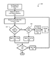
- FIG. 6 is a flow diagram of a method 620 according to an embodiment.
- a method can include setting an initial energy value (Ex) 618 .
- Such an action can include setting the characteristics of one or more electric pulses that will be applied to a group of cells to set a resistance of their element(s). Such characteristics can include, but are not limited to, voltage magnitude, pulse duration, number of pulses, pulse shape, or current compliance (e.g., maximum and/or minimum current allowed to flow). All cells can be selected for an initial resistance setting operation 622 (only out of compliance elements being subject to follow on-operations).
- a method 620 can include applying a current energy (Ex) to the current selected set of cells to set the resistance of such cells 624 . It is understood that a first iteration can include all elements at the initial Ex value.
- An action 624 can include applying the energy to cells individually, or to multiple cells simultaneously, or combinations thereof. In a particular embodiment, an initial setting operation (to all cells) can be simultaneous, while follow-on setting operations (to cells out of compliance) can be done to individual elements.
- a cell resistance can be checked to see if it is in a desired verification range (Ver Range) 626 (i.e., if the cell is in compliance with a current resistance range). If Rcell is within a current Ver Range (Y from 626 ), it is marked as passing 630 . If Rcell is not within a current Ver Range (N from 626 ), optionally, a check can be made to see of a maximum number of tries (i.e., follow-on resistance setting operations) has been reached 632 . If a maximum number of tries has been reached (Y from 632 ), a cell can be marked as failing 634 .
- Ver Range desired verification range
- a method 620 can change a current Ver Range to one that is closer to a read threshold value (Rth) 636 .
- the change in Ver Range sets a verify resistance for a next, follow-on resistance setting operation.
- Rth can be a resistance value at which a determination can be made between logic values stored by a cell (i.e., if Rcell>Rth, it can store a “0”, and if Rcell ⁇ Rth, it can store a “1”).
- a new energy (Ex) can be set 638 .
- Ex can be kept the same for some, or all follow-on resistance setting operations.
- follow-on resistance setting operations can proceed by returning to 624 .
- a cell has been marked as pass or fail, if it is a last cell (Y from 640 ) an operation 620 can end. If it is not last cell (N from 640 ), a next cell can be selected 624 , and an operation can return to 624 .
- FIG. 7 shows a method 720 according to another embodiment.
- a method 720 can be an erase method for programmable resistance elements.
- a method 720 can erase elements to a high resistance for subsequent programming to a low resistance according to a data value to be stored.
- a method 720 can include erasing a group of programmable resistance elements by applying an electric field of energy Einit 744 .
- such an action can include applying one or more voltage pulses across the terminals of the elements.
- a resistance of the elements can be verified to be greater than a verification resistance R_ver 746 .
- Each element that fails the verification step can be subject to a follow-on erase operation at an energy Ex 724 .
- Such an erase operation can apply an electric field in the same direction as that of the initial erase operation ( 744 ).
- Ex can be the same as Einit.
- Ex can be different from Einit.
- An erase verification resistance R_ver can be lowered 736 , and an element resistance can be verified to be greater than the lower R_ver 726 .
- Such a lower follow-on verification resistance can be subject to the variations described for embodiments herein.
- an erase energy (Ex) can be increased for a next follow-on erase operation 738 .
- a method 720 can determine a maximum number of iterations has been performed 732 . If a maximum number of iterations has not been reached (N from 732 ), a method can return to 724 and execute another follow erase and verify operation at an even lower resistance. If a maximum number of iterations has been reached (Y from 732 ), a method can end.
- FIG. 8 is a flow diagram of a method 820 according to a particular embodiment.
- a method 820 show operations for erasing CBRAM type elements to a high resistance, which can move very low resistance tail elements to a high resistance, while reducing the chance of “reverse programming” elements back to a low resistance.
- a method 820 can be preceded by an initial erase operation, which can attempt to erase an element to a high resistance state.
- a method 820 can include setting a count N to an initial value 848 .
- a count value N can determine how many follow-on erase and verify operations an element can be subject to.
- An attempt value (ATTEMPT) can also be set to an initial value 850 .
- An attempt value can be number of times a method will perform follow-on erase and verify operations on an element at a particular set of values (e.g., erase energy and verify resistance).
- Elements can be subject to a “post” resistance verification at a resistance level ERV 1 ( n ) 846 . It is noted that such a level can be subject to variation as described herein. If an element is within compliance (Y from 846 ), the element can be considered properly erased, and the method can end.
- method 820 can proceed to an inner loop 852 .
- elements can be subject to follow-on erase and verify operations.
- inner loop 852 can include applying an erase stress to an element 824 .
- this erase stress can be the same for all follow-on erase operations (i.e., counts of N).
- erase stress can vary between follow-on operations.
- an element can be subject to a “pre” resistance verification at a resistance level ERV 2 ( n ) 826 .
- a value of ERV 2 ( n ) can vary for each follow-on erase operation.
- ERV 2 ( n ) can be lower with each higher value of N. If an element's resistance is greater than ERV 2 ( n ) (Y from 826 ), its status can be set to “pass” 830 and a value of N can be incremented 856 .
- a maximum attempt limit (MAXATTEMPT(n)) can vary with each follow-on operation (i.e., each value of N).
- a check can be made to see if a maximum value for N has been reached ( 858 ) (i.e., it was the last follow-on operation). If a maximum value for N is not reached (N from 858 ), a method 820 can proceed to a next follow-on operation, by returning to 850 , to reset the ATTEMPT value, and proceeding to another “pre” resistance verify 846 . If a maximum value for N is reached (Y from 858 ), a method 820 can end with an element having a particular status (i.e., pass or fail).
- a method 820 can include values like those of FIG. 4C . Where N can be 5, the value of ERV 1 ( n ) remains at 1 M, and the value of ERV 2 ( n ) follows those of the PRE column.
- FIG. 9 is a block diagram of a device 900 according to an embodiment.
- a device 900 can include one or more memory cell arrays 960 , access circuits 962 , verify circuits 964 , program/erase circuits 966 , and a controller 970 .
- Memory cell array 960 can include memory cells that each include one or more programmable resistance elements that are programmable between different resistance states by application of electric fields.
- each memory cell can include an access device, such as a transistor, and a two terminal element.
- each memory cell can include more than one element and/or more than one access device.
- memory cells can be formed by but one element (e.g., arranged in a cross point array configuration).
- each memory cell can include an n-channel type transistor and a CBRAM type element.
- Access circuits 962 can enable access to memory cells according to address values ADD.
- access circuits 962 can include decoder circuits, including row and/or column decoders.
- access circuits 962 can also provide limited access to some memory cells (e.g., boot blocks or the like).
- Verify circuits 964 check if a resistance of memory cells (or their elements) is within a range. Such ranges can be single ended (e.g., some minimum resistance or some maximum resistance), or can be bounded (e.g., a minimum and maximum). According to embodiments, verify circuits 964 are designed to verify at least two different resistance levels (i.e., an initial verify resistance and at least one follow-on resistance). In the particular embodiment shown, a verify resistance for a verify circuit 964 can be determined by a control input Rver SEL. Verify circuits 964 can perform resistance verify operations according to the embodiments described herein, or equivalents.
- Program/erase circuits 966 can set a resistance of memory cells by application of an electric field through access circuits 962 .
- memory cells within array(s) 960 can be erased to a high resistance than selectively programmed to one or more lower resistances according to a data value to be stored.
- memory cells can be erased to a low resistance and selectively programmed to a high resistance.
- erase operations can be controlled according to erase control inputs Erase Ctrl.
- a controller 970 can control erase and verify operations to perform operations as described herein, or equivalents.
- controller 970 can provide control inputs Rver SEL and Erase Ctrl to verify circuits 964 and program/erase circuits 966 that enable such circuits to perform initial erase and verify operations, followed by one or more follow-on erase and verify operations at different resistance levels, according to embodiments described herein, or equivalents.
- a device 900 can include an erase energy source 974 that can provide an erase energy Ex to program/erase circuits 974 .
- the amount of energy Ex provided can be selectable according to a value Ex SEL.
- energy source 974 can provide erase voltage pulses that can vary as noted herein or equivalents (e.g., voltage magnitude, duration, shape, etc.). In this way, according to values Ex SEL provided by controller 970 , erase energies can be varied between different follow-on erase operations.
- a device 900 can also include a verify memory 972 .
- a verify memory 972 can store values for memory cells undergoing follow-on erase and verify operations.
- a controller 970 can track a location (e.g., address) for each memory cell undergoing a follow-on operation, as well as its current verification resistance, current erase energy, and any other variables used in the operations (e.g., maximum attempts for each follow-on operation, maximum number of follow-on operations, etc.).
- FIGS. 10A to 10C are diagrams showing examples of a verify memory 1072 that can be included in embodiments.
- a verify memory 1072 can store information on memory cells that fail an initial erase and verify, and are subject to follow-on erase and verify operations.
- verify memory 1072 can include address information (ADD), a current verify resistance level (Rver Level), a current erase energy level (Ex Level), and a status value (STATUS).
- ADD address information
- RV Level current verify resistance level
- Ex Level current erase energy level
- STATUS status value
- FIG. 10A shows a verify memory 1072 following an initial erase and verify operation. Data for elements that do not comply with the initial verify resistance are stored. While a STATUS value shows FAIL, in other embodiments, at this initial point in operation such a value may not be set, and so can be considered “not valid”.
- FIG. 10B shows a verify memory 1072 following a first follow-on erase and verify operation. As shown, three memory cell/elements have recovered, while two memory cell/elements are (or remain) failing bits.
- the follow-on erase and verify is performed at a different verify resistance that is closer to a read verify resistance.
- FIG. 10C shows a verify memory 1072 following a second follow-on erase and verify operation.
- Those memory cell/elements with a fail status can be subject to another follow-on erase and verify operation.
- this follow-on erase and verify can be performed at a different verify resistance that is closer to a read verify resistance than the previous verify resistance.
- Embodiments herein can utilize any suitable programmable resistance element providing the response noted.
- elements change resistance in response to an applied electric field, but do not change resistance by thermal phase change event, such as the transition from a crystalline to amorphous state.
- FIGS. 11A to 11C are side cross sectional representations of an element 1176 that can be included in embodiments.
- Element 1176 can be a two terminal element having one or more resistance change layers 1180 disposed between a first electrode 1178 and a second electrode 1182 .
- FIG. 11A shows an element 1176 in one state in which a resistance between the two electrodes ( 1178 and 1182 ) can have one value R 1 .
- FIG. 11B shows element responses in a first part of a resistance setting (e.g., erase) operation.
- An electric field Ex is applied across the element 1176 .
- an erase operation can include an oxidation-reduction reaction.
- positive ion 1186 an erase operation can result in ion conduction.
- other embodiments may not include ion conduction.
- a resistance of resistance change layer(s) may be unchanged, changed only a small amount, or undergoing change (represented by Rx).
- FIG. 11C shows an element after the resistance setting operation.
- a resistance of resistance change layer(s) may have changed (R 2 ⁇ R 1 ).
- an electric field opposite to that of FIG. 11B can be applied to change a resistance opposite to that represented by FIGS. 11A to 11C .
- FIG. 12 is a plan view of an integrated circuit (IC) device 1200 according to an embodiment.
- a device 1200 can include any or all of the various circuit components shown in FIG. 9 and/or can include memory cells and circuits for executing the various methods described herein or equivalents.
- an IC device 1200 can include memory cells that store data with greater endurance than conventional devices, which do not include methods for addressing “tail” distribution memory cells/element(s).
- embodiments can include IC device and methods, other embodiments can include electronic devices having operational lifetimes that are increased by including erase and verify methods as described herein, or equivalents.
- One very particular example of such a device is shown in FIG. 13 .
- FIG. 13 is a perspective view of a personal medical monitoring (PMM) device 1300 .
- PMM device 1300 can be worn by a person, and record and/or store data regarding the wearer's health in a nonvolatile memory composed of programmable resistance elements.
- the lifetime of the device can be an important feature, as changing devices can require data transfers and/or failure of the device can lose data and/or jeopardize the wearer's health.
- Inclusion of erase and verify methods that detect and correction “tail” elements, as described in embodiments herein or equivalents, can result in the lifetime of the device 1300 being extended as compared to a conventional device.
Abstract
Description
Claims (19)
Priority Applications (1)
| Application Number | Priority Date | Filing Date | Title |
|---|---|---|---|
| US14/927,352 US9613693B1 (en) | 2015-10-29 | 2015-10-29 | Methods for setting a resistance of programmable resistance memory cells and devices including the same |
Applications Claiming Priority (1)
| Application Number | Priority Date | Filing Date | Title |
|---|---|---|---|
| US14/927,352 US9613693B1 (en) | 2015-10-29 | 2015-10-29 | Methods for setting a resistance of programmable resistance memory cells and devices including the same |
Publications (1)
| Publication Number | Publication Date |
|---|---|
| US9613693B1 true US9613693B1 (en) | 2017-04-04 |
Family
ID=58419548
Family Applications (1)
| Application Number | Title | Priority Date | Filing Date |
|---|---|---|---|
| US14/927,352 Active US9613693B1 (en) | 2015-10-29 | 2015-10-29 | Methods for setting a resistance of programmable resistance memory cells and devices including the same |
Country Status (1)
| Country | Link |
|---|---|
| US (1) | US9613693B1 (en) |
Cited By (2)
| Publication number | Priority date | Publication date | Assignee | Title |
|---|---|---|---|---|
| WO2019193423A1 (en) * | 2018-04-05 | 2019-10-10 | Commissariat A L'energie Atomique Et Aux Energies Alternatives | Circuit and method for programming resistive memory cells |
| US10984861B1 (en) | 2017-07-12 | 2021-04-20 | Adesto Technologies Corporation | Reference circuits and methods for resistive memories |
Citations (17)
| Publication number | Priority date | Publication date | Assignee | Title |
|---|---|---|---|---|
| US20040109353A1 (en) * | 2002-12-04 | 2004-06-10 | Sharp Kabushiki Kaisha | Semiconductor memory device and method for correcting a reference cell |
| US20060126391A1 (en) * | 2004-12-09 | 2006-06-15 | Bo-Geun Kim | Methods of program verifying non-volatile memory devices |
| US7167390B2 (en) | 2003-05-27 | 2007-01-23 | Sony Corporation | Storage device with resistive memory cells enduring repetitive data writing |
| US7327603B2 (en) | 2005-08-16 | 2008-02-05 | Infineon Technologies Ag | Memory device including electrical circuit configured to provide reversible bias across the PMC memory cell to perform erase and write functions |
| US20080074918A1 (en) * | 2006-09-27 | 2008-03-27 | Yu-Hwan Ro | Phase change memory device and related programming method |
| US20090040816A1 (en) * | 2007-08-10 | 2009-02-12 | Hee Bok Kang | Method for driving a phase change memory device using various write conditions |
| US20100027326A1 (en) * | 2008-07-30 | 2010-02-04 | Ho Jung Kim | Memory device, memory system having the same, and programming method of a memory cell |
| US7715220B2 (en) | 2006-06-07 | 2010-05-11 | Sony Corporation | Memory apparatus |
| US8331128B1 (en) | 2008-12-02 | 2012-12-11 | Adesto Technologies Corporation | Reconfigurable memory arrays having programmable impedance elements and corresponding methods |
| US8369132B1 (en) | 2008-07-28 | 2013-02-05 | Adesto Technologies Corporation | Methods of programming and erasing programmable metallization cells (PMCs) |
| US8531863B2 (en) | 2005-05-20 | 2013-09-10 | Adesto Technologies Corporation | Method for operating an integrated circuit having a resistivity changing memory cell |
| US20140269045A1 (en) * | 2013-03-14 | 2014-09-18 | Daniel J. Chu | Cell programming verification |
| US8902631B2 (en) | 2012-08-30 | 2014-12-02 | Adesto Technologies Corporation | Memory devices, circuits and, methods that apply different electrical conditions in access operations |
| US8934292B2 (en) * | 2011-03-18 | 2015-01-13 | Sandisk 3D Llc | Balanced method for programming multi-layer cell memories |
| US8976568B1 (en) | 2012-01-20 | 2015-03-10 | Adesto Technologies Corporation | Circuits and methods for programming variable impedance elements |
| US9025396B1 (en) | 2012-02-08 | 2015-05-05 | Adesto Technologies Corporation | Pre-conditioning circuits and methods for programmable impedance elements in memory devices |
| US9336880B2 (en) * | 2014-07-16 | 2016-05-10 | Kabushiki Kaisha Toshiba | Nonvolatile memory device and method of controlling the same |
-
2015
- 2015-10-29 US US14/927,352 patent/US9613693B1/en active Active
Patent Citations (19)
| Publication number | Priority date | Publication date | Assignee | Title |
|---|---|---|---|---|
| US20040109353A1 (en) * | 2002-12-04 | 2004-06-10 | Sharp Kabushiki Kaisha | Semiconductor memory device and method for correcting a reference cell |
| US7167390B2 (en) | 2003-05-27 | 2007-01-23 | Sony Corporation | Storage device with resistive memory cells enduring repetitive data writing |
| US20060126391A1 (en) * | 2004-12-09 | 2006-06-15 | Bo-Geun Kim | Methods of program verifying non-volatile memory devices |
| US8531863B2 (en) | 2005-05-20 | 2013-09-10 | Adesto Technologies Corporation | Method for operating an integrated circuit having a resistivity changing memory cell |
| US7327603B2 (en) | 2005-08-16 | 2008-02-05 | Infineon Technologies Ag | Memory device including electrical circuit configured to provide reversible bias across the PMC memory cell to perform erase and write functions |
| US7715220B2 (en) | 2006-06-07 | 2010-05-11 | Sony Corporation | Memory apparatus |
| US20080074918A1 (en) * | 2006-09-27 | 2008-03-27 | Yu-Hwan Ro | Phase change memory device and related programming method |
| US20090040816A1 (en) * | 2007-08-10 | 2009-02-12 | Hee Bok Kang | Method for driving a phase change memory device using various write conditions |
| US8625331B1 (en) | 2008-07-28 | 2014-01-07 | Adesto Technologies Corporation | Methods of programming and erasing programmable metallization cells (PMCs) |
| US8369132B1 (en) | 2008-07-28 | 2013-02-05 | Adesto Technologies Corporation | Methods of programming and erasing programmable metallization cells (PMCs) |
| US20100027326A1 (en) * | 2008-07-30 | 2010-02-04 | Ho Jung Kim | Memory device, memory system having the same, and programming method of a memory cell |
| US8331128B1 (en) | 2008-12-02 | 2012-12-11 | Adesto Technologies Corporation | Reconfigurable memory arrays having programmable impedance elements and corresponding methods |
| US9007814B1 (en) | 2008-12-02 | 2015-04-14 | Adesto Technologies Corporation | Application of relaxation voltage pulses to programmble impedance elements during read operations |
| US8934292B2 (en) * | 2011-03-18 | 2015-01-13 | Sandisk 3D Llc | Balanced method for programming multi-layer cell memories |
| US8976568B1 (en) | 2012-01-20 | 2015-03-10 | Adesto Technologies Corporation | Circuits and methods for programming variable impedance elements |
| US9025396B1 (en) | 2012-02-08 | 2015-05-05 | Adesto Technologies Corporation | Pre-conditioning circuits and methods for programmable impedance elements in memory devices |
| US8902631B2 (en) | 2012-08-30 | 2014-12-02 | Adesto Technologies Corporation | Memory devices, circuits and, methods that apply different electrical conditions in access operations |
| US20140269045A1 (en) * | 2013-03-14 | 2014-09-18 | Daniel J. Chu | Cell programming verification |
| US9336880B2 (en) * | 2014-07-16 | 2016-05-10 | Kabushiki Kaisha Toshiba | Nonvolatile memory device and method of controlling the same |
Cited By (3)
| Publication number | Priority date | Publication date | Assignee | Title |
|---|---|---|---|---|
| US10984861B1 (en) | 2017-07-12 | 2021-04-20 | Adesto Technologies Corporation | Reference circuits and methods for resistive memories |
| WO2019193423A1 (en) * | 2018-04-05 | 2019-10-10 | Commissariat A L'energie Atomique Et Aux Energies Alternatives | Circuit and method for programming resistive memory cells |
| US11217307B2 (en) | 2018-04-05 | 2022-01-04 | Commissariat à l'Energie Atomique et aux Energies Alternatives | Circuit and method for programming resistive memory cells |
Similar Documents
| Publication | Publication Date | Title |
|---|---|---|
| US9001561B2 (en) | Performing forming processes on resistive memory | |
| TWI774436B (en) | Techniques for initializing resistive memory devices | |
| US9711216B2 (en) | Semiconductor storage device | |
| US9269432B2 (en) | Memory systems and memory programming methods | |
| CN108701486A (en) | It is generated using the PUF values of antifuse memory array | |
| US7259983B2 (en) | Page buffer architecture for programming, erasing and reading nanoscale resistive memory devices | |
| US9627060B2 (en) | Memory circuit and method of programming memory circuit | |
| US10580506B2 (en) | Semiconductor memory device and erase method including changing erase pulse magnitude for a memory array | |
| US20190279714A1 (en) | Memory Systems and Memory Programming Methods | |
| US8942035B2 (en) | Non-sequential encoding scheme for multi-level cell (MLC) memory cells | |
| US20140059268A1 (en) | Memory control device, non-volatile memory, and memory control method | |
| US8995167B1 (en) | Reverse program and erase cycling algorithms | |
| JP2016134193A (en) | Memory cell array of resistance change type random access memory | |
| US20080285368A1 (en) | Method for nrom array word line retry erasing and threshold voltage recovering | |
| JP7236592B2 (en) | Method for Improving Read Current Stability in Analog Non-Volatile Memories by Screening Memory Cells | |
| CN110060722B (en) | Power-on reset method of resistive memory storage device | |
| US9613693B1 (en) | Methods for setting a resistance of programmable resistance memory cells and devices including the same | |
| JP6482959B2 (en) | Semiconductor memory device | |
| US9025396B1 (en) | Pre-conditioning circuits and methods for programmable impedance elements in memory devices | |
| WO2020209885A1 (en) | Reram programming method including low-current pre-programming for program time reduction | |
| JP5327900B2 (en) | Method of using an electronic device having a non-volatile memory array | |
| US9418737B2 (en) | Nonvolatile semiconductor memory device and method of controlling the same | |
| US9524777B1 (en) | Dual program state cycling algorithms for resistive switching memory device | |
| US8391069B2 (en) | Programming method for nonvolatile semiconductor memory device | |
| US20230008586A1 (en) | Method for resetting an array of resistive memory cells |
Legal Events
| Date | Code | Title | Description |
|---|---|---|---|
| AS | Assignment |
Owner name: ADESTO TECHNOLOGIES CORPORATION, CALIFORNIA Free format text: ASSIGNMENT OF ASSIGNORS INTEREST;ASSIGNOR:KAMALANATHAN, DEEPAK;REEL/FRAME:036918/0370 Effective date: 20151023 |
|
| STCF | Information on status: patent grant |
Free format text: PATENTED CASE |
|
| AS | Assignment |
Owner name: OBSIDIAN AGENCY SERVICES, INC., AS COLLATERAL AGENT, CALIFORNIA Free format text: SECURITY INTEREST;ASSIGNORS:ADESTO TECHNOLOGIES CORPORATION;ARTEMIS ACQUISITION LLC;REEL/FRAME:046105/0731 Effective date: 20180508 Owner name: OBSIDIAN AGENCY SERVICES, INC., AS COLLATERAL AGEN Free format text: SECURITY INTEREST;ASSIGNORS:ADESTO TECHNOLOGIES CORPORATION;ARTEMIS ACQUISITION LLC;REEL/FRAME:046105/0731 Effective date: 20180508 |
|
| AS | Assignment |
Owner name: ARTEMIS ACQUISITION LLC, CALIFORNIA Free format text: RELEASE BY SECURED PARTY;ASSIGNOR:OBSIDIAN AGENCY SERVICES, INC., AS COLLATERAL AGENT;REEL/FRAME:050480/0836 Effective date: 20190923 Owner name: ADESTO TECHNOLOGIES CORPORATION, CALIFORNIA Free format text: RELEASE BY SECURED PARTY;ASSIGNOR:OBSIDIAN AGENCY SERVICES, INC., AS COLLATERAL AGENT;REEL/FRAME:050480/0836 Effective date: 20190923 |
|
| MAFP | Maintenance fee payment |
Free format text: PAYMENT OF MAINTENANCE FEE, 4TH YEAR, LARGE ENTITY (ORIGINAL EVENT CODE: M1551); ENTITY STATUS OF PATENT OWNER: LARGE ENTITY Year of fee payment: 4 |
|
| AS | Assignment |
Owner name: GLOBALFOUNDRIES U.S. INC., NEW YORK Free format text: ASSIGNMENT OF ASSIGNORS INTEREST;ASSIGNOR:RENESAS DESIGN US INC. (FORMERLY KNOWN AS DIALOG SEMICONDUCTOR US INC. AS SUCCESSOR-IN-INTEREST TO ADESTO TECHNOLOGIES CORPORATION AND ARTEMIS ACQUISITION, LLC);REEL/FRAME:063118/0352 Effective date: 20230203 |