JP4295110B2 - Display device, receiving device, and test device - Google Patents
Display device, receiving device, and test device Download PDFInfo
- Publication number
- JP4295110B2 JP4295110B2 JP2003543326A JP2003543326A JP4295110B2 JP 4295110 B2 JP4295110 B2 JP 4295110B2 JP 2003543326 A JP2003543326 A JP 2003543326A JP 2003543326 A JP2003543326 A JP 2003543326A JP 4295110 B2 JP4295110 B2 JP 4295110B2
- Authority
- JP
- Japan
- Prior art keywords
- test
- circuit
- data
- display device
- inspection
- Prior art date
- Legal status (The legal status is an assumption and is not a legal conclusion. Google has not performed a legal analysis and makes no representation as to the accuracy of the status listed.)
- Expired - Fee Related
Links
Images


Classifications
-
- H—ELECTRICITY
- H04—ELECTRIC COMMUNICATION TECHNIQUE
- H04N—PICTORIAL COMMUNICATION, e.g. TELEVISION
- H04N7/00—Television systems
- H04N7/12—Systems in which the television signal is transmitted via one channel or a plurality of parallel channels, the bandwidth of each channel being less than the bandwidth of the television signal
-
- H—ELECTRICITY
- H04—ELECTRIC COMMUNICATION TECHNIQUE
- H04N—PICTORIAL COMMUNICATION, e.g. TELEVISION
- H04N17/00—Diagnosis, testing or measuring for television systems or their details
- H04N17/04—Diagnosis, testing or measuring for television systems or their details for receivers
Description
本発明は、試験対象としてのディスプレイ装置及びその関連技術に関する。 The present invention relates to a display device as a test object and related technology.
従来より、デジタル映像データの高速伝送を実行する技術に関する規格として、1999年4月2日に公表された規格書「Digital Visual Interface Revision1.0」(以下、「DVI規格書」と呼ぶ。)がある(http://WWW.ddwg.org/)。 Conventionally, a standard document “Digital Visual Interface Revision 1.0” (hereinafter referred to as “DVI standard document”) published on April 2, 1999 is a standard related to a technique for performing high-speed transmission of digital video data. Yes (http://WWW.ddwg.org/).
図23は、DVI規格書に従って構成された一般的なデジタル映像データ送受信システムのブロック図である。 FIG. 23 is a block diagram of a general digital video data transmission / reception system configured in accordance with the DVI standard.
図23に示すように、このデジタル映像データ送受信システムは、映像データ送信装置500、ケーブル501、及び、ディスプレイ装置502、を具備する。 As shown in FIG. 23, this digital video data transmission / reception system includes a video data transmission device 500, a cable 501, and a display device 502.
映像データ送信装置500とディスプレイ装置502とは、ケーブル501により接続される。 The video data transmission device 500 and the display device 502 are connected by a cable 501.
映像データ送信装置500は、映像生成回路503、データ送信回路504、クロック信号発生回路505、コントロール信号送信回路506、及び、コントロール信号受信回路507、を含む。
The video data transmission device 500 includes a
ディスプレイ装置502は、受信LSI(受信集積回路)508及び表示ユニット509を含む。この受信LSI508は、データ受信回路510、PLL(phase locked loop)回路511、コントロール信号受信回路512、及び、コントロール信号送信回路513、を含む。
The display device 502 includes a reception LSI (reception integrated circuit) 508 and a
さて、動作を簡単に説明する。 Now, the operation will be briefly described.
図23に示すように、映像データ送信装置500のコントロール信号送信回路506は、映像データを送信する旨を通知するコントロール信号を、ケーブル501を介して、ディスプレイ装置502のコントロール信号受信回路512へ送信する。
As shown in FIG. 23, the control
すると、コントロール信号受信回路512は、そのコントロール信号を受信する。
Then, the control
すると、ディスプレイ装置502のコントロール信号送信回路513は、ディスプレイ装置502の解像度などの表示制御情報を、ケーブル501を介して、映像データ送信装置500のコントロール信号受信回路507に送信する。
Then, the control
映像データ送信装置500のクロック信号発生回路505は、クロック信号を発生し、映像生成回路503と、ディスプレイ装置502のPLL回路511と、に送信する。
The clock signal generation circuit 505 of the video data transmission device 500 generates a clock signal and transmits it to the
映像生成回路503は、クロック信号発生回路505が供給するクロック信号に同期して、映像データを出力する。
The
そして、データ送信回路504は、映像生成回路503が出力した映像データを、ケーブル501を介して、ディスプレイ装置502のデータ受信回路510へ送信する。
Then, the
ディスプレイ装置502のデータ受信回路510は、PLL回路511がクロック信号に同期して生成したタイミング信号に同期して、映像データを取り込む。
The
データ受信回路510は、取り込んだ映像データを表示ユニット509へ出力し、表示ユニット509は、これを表示する。
The
従来、このようなデジタル映像データ送受信システムの動作確認は、表示ユニット509に表示された映像の乱れを目視検査するか、あるいは、データ誤り率を測定することにより行っていた。
Conventionally, the operation check of such a digital video data transmission / reception system has been performed by visually inspecting the disturbance of the video displayed on the
しかしながら、このような目視検査の場合には、検査者の能力によって検査結果に違いが出たり、また、熟練した検査者であっても僅かな乱れや、瞬間的な乱れを見逃す、といった問題があった。 However, in the case of such a visual inspection, there are problems such as differences in inspection results depending on the ability of the inspector, and even a skilled inspector misses slight disturbances or instantaneous disturbances. there were.
一方、従来、データ誤り率の測定は、受信LSI508が備える回路と同様の機能を有する試作基板に、誤り率測定用基板を接続して行っていた。
On the other hand, conventionally, the measurement of the data error rate has been performed by connecting the error rate measurement substrate to a prototype substrate having the same function as the circuit included in the
しかし、実際の製品開発においては、最終的なディスプレイ装置502の試作機に対しても試験を行う必要がある。 However, in actual product development, it is necessary to test the final display device 502 prototype.
この場合、従来では、ディスプレイ装置502を組み立てる前に、内部の基板に誤り率測定用基板を接続して、データ誤り率を測定していた。 In this case, conventionally, before assembling the display device 502, an error rate measurement board is connected to an internal board to measure the data error rate.
しかし、ディスプレイ装置502を組み立てる前と後では、ノイズ環境が変化してしまう。特に、ディスプレイ装置502は、映像データ送信装置500からのギガヘルツに及ぶ高速伝送されたデータを受信するため、ディスプレイ装置502に設けられたデータ受信回路510等の回路は、ノイズ環境に強く依存する。
However, the noise environment changes before and after the display device 502 is assembled. In particular, since the display device 502 receives data transmitted at a high speed up to gigahertz from the video data transmission device 500, circuits such as the
このため、ディスプレイ装置502を組み立てる前と後では、ノイズ環境が必ずしも一致しない場合もあり、より正確な検査が求められていた。 For this reason, before and after assembling the display device 502, the noise environments may not always match, and a more accurate inspection is required.
また、ディスプレイ装置502を組み立てた後に、何らかの不具合が判明し、再検査が必要になった場合、ディスプレイ装置502を分解し、誤り率測定用基板とディスプレイ装置502の内部の基板とを接続する、という手間がかかるという問題があった。 Further, when some trouble is found after the display device 502 is assembled and re-examination is necessary, the display device 502 is disassembled, and the error rate measurement substrate and the substrate inside the display device 502 are connected. There was a problem that it took time and effort.
また、ディスプレイ装置502の内部の基板上に誤り率測定用基板と接続するためのコネクタを別途実装しなければならず、そのため、実装面積が増大し、製造上の手間もかかるという問題があった。 In addition, a connector for connecting to the error rate measurement board must be separately mounted on the board inside the display device 502, which causes a problem that the mounting area is increased and the manufacturing is troublesome. .
また、テスト条件の設定は人間が手動で行っていたため、その設定のための手間がかかるという問題があった。 In addition, since the test conditions are set manually by humans, there is a problem that it takes time and effort.
また、PLL回路511の動作確認をすることは重要であるが、DVI規格書に記載されている方法では、データ誤り率を観測することで間接的にPLL回路511が誤動作している可能性を推測できるだけであり、PLL回路511の誤動作そのものを検出する手段が示されていない。 It is important to confirm the operation of the PLL circuit 511. However, in the method described in the DVI standard document, the possibility of the PLL circuit 511 malfunctioning indirectly by observing the data error rate. It can only be estimated, and no means for detecting the malfunction of the PLL circuit 511 is shown.
このため、ディスプレイ装置502が誤動作したときに、その原因が、PLL回路511の誤動作にあるのか、それとも他の伝送劣化要因(ケーブル減衰やスキュー等)にあるのかを断定することが困難なため、試行錯誤が必要となり、対策に時間がかかるという問題があった。 For this reason, when the display device 502 malfunctions, it is difficult to determine whether the cause is malfunction of the PLL circuit 511 or other transmission deterioration factors (cable attenuation, skew, etc.) Trial and error was necessary, and there was a problem that it took time to take measures.
また、ディスプレイ装置502を組み立てた後に、データ誤り率の測定やPLL回路511の誤動作を検査する方法として、検査結果を表す信号を出力する端子をディスプレイ装置502の外部に設けることが考えられる。 In addition, as a method of measuring the data error rate and inspecting the malfunction of the PLL circuit 511 after assembling the display device 502, it is conceivable to provide a terminal for outputting a signal representing the inspection result outside the display device 502.
しかし、ディスプレイ装置502の外観も売れ行きの重要な要素となっている昨今において、一般ユーザにとって必ずしも必要のない上記端子が外部に露出するのは好ましくないという問題がある。 However, in recent years when the appearance of the display device 502 is also an important factor in sales, there is a problem that it is not preferable that the above-described terminals that are not necessarily required by general users are exposed to the outside.
また、検査結果を表す信号を生成する回路が、受信LSI508に内蔵されている場合、検査結果を表す信号を受信LSI508の外部に出力するためのピンを設ける必要がある。
In addition, when a circuit that generates a signal representing a test result is built in the
しかし、この場合、受信LSI508のピンが増えることで、実装面積の増加や、既にに開発されたLSIとのピン互換性喪失(部材互換性喪失)といった問題が生じる。
そこで、本発明は、ディスプレイ装置内部のノイズ環境を変えることなく、ディスプレイ装置内部のデータ受信に係わる回路の試験を簡易に実行でき、かつ、その試験結果をディスプレイ装置外部に取り出すために新たに部材を設けることを不要とし、実装面積の増加及び部材互換性喪失(他のLSIとのピン互換性喪失)といった不都合を回避でき、しかも、ディスプレイ装置の誤動作の原因を極力具体的に特定できるディスプレイ装置及びその関連技術を提供することを目的とする。 Therefore, the present invention can easily execute a test of a circuit related to data reception inside the display device without changing the noise environment inside the display device, and is a new member for taking out the test result outside the display device. The display device can avoid the inconveniences such as increase in mounting area and loss of component compatibility (loss of pin compatibility with other LSIs), and can identify the cause of malfunction of the display device as much as possible. And its related technology.
第1の発明に係るディスプレイ装置では、通常モードにおいて、映像データを受信し、試験モードにおいて、テスト信号を受信するデータ受信に係わるユニットと、試験モードにおいて、データ受信に係わるユニットを検査し、検査情報を生成する検査ユニットと、検査情報を表す画像データを生成する検査結果画像生成ユニットと、試験モードにおいて、検査結果画像生成ユニットが生成した画像データを表示し、通常モードにおいて、映像データを表示する表示ユニットと、を備え、データ受信に係わるユニットは、通常モードにおいて、受信したクロック信号に同期したタイミング信号を発生し、試験モードにおいて、テスト信号としてのジッタを含むクロック信号を受信し、受信したクロック信号に同期したタイミング信号を発生する位相同期ループユニット、を含み、検査ユニットは、試験モードにおいて、位相同期ループユニットの誤動作情報を生成する誤動作情報生成ユニット、を含み、検査結果画像生成ユニットは、誤動作情報生成ユニットが生成した誤動作情報を表す画像データを生成する。 In the display device according to the first aspect of the invention, in the normal mode, the video data is received, and in the test mode, the unit related to data reception for receiving the test signal and the unit related to data reception in the test mode are inspected. An inspection unit that generates information, an inspection result image generation unit that generates image data representing inspection information, and image data generated by the inspection result image generation unit in the test mode are displayed, and video data is displayed in the normal mode. A display unit that receives the clock signal including jitter as a test signal in the test mode and generates a timing signal synchronized with the received clock signal in the normal mode. Generate a timing signal synchronized with the clock signal A phase locked loop unit, and the inspection unit includes a malfunction information generation unit that generates malfunction information of the phase locked loop unit in the test mode, and the inspection result image generation unit includes malfunction information generated by the malfunction information generation unit. Is generated .
この構成により、ディスプレイ装置内部で、データ受信に係わるユニットが検査され、検査情報が生成される。 With this configuration, a unit related to data reception is inspected inside the display device, and inspection information is generated.
そして、生成された検査情報が、ディスプレイ装置が備える表示ユニットに表示される。 And the produced | generated test | inspection information is displayed on the display unit with which a display apparatus is provided.
その結果、ディスプレイ装置の組立後に、しかも、ディスプレイ装置の分解をすることなく、検査が可能となって、ディスプレイ装置内部のノイズ環境を変えることなく、ディスプレイ装置内部のデータ受信に係わるユニットの試験を簡易に実行できる。 As a result, after assembling the display device, it is possible to inspect without disassembling the display device, and to test the unit related to data reception inside the display device without changing the noise environment inside the display device. Easy to execute.
また、検査情報を表す画像データは、ディスプレイ装置が備える表示ユニットに表示されるため、検査情報を表す画像データを出力する端子を、ディスプレイ装置の外部に新たに設けることが不要になる。 Further, since the image data representing the inspection information is displayed on the display unit included in the display device, it is not necessary to newly provide a terminal for outputting the image data representing the inspection information outside the display device.
第2の発明に係るディスプレイ装置では、通常モードにおいて、映像データを受信し、試験モードにおいて、テスト信号を受信するデータ受信に係わるユニットと、試験モードにおいて、データ受信に係わるユニットを検査し、検査情報を生成する検査ユニットと、検査情報を外部に送信するユニットと、通常モードにおいて、映像データを表示する表示ユニットと、を備え、試験モードにおいて、データ受信に係わるユニットは、外部から、検査情報を表す画像データを受信し、試験モードにおいて、表示ユニットは、検査情報を表す画像データを表示する。 In the display device according to the second invention, in the normal mode, the video data is received, and in the test mode, the unit related to data reception that receives the test signal and the unit related to data reception in the test mode are inspected. A test unit for generating information; a unit for transmitting test information to the outside; and a display unit for displaying video data in the normal mode. In the test mode, the display unit displays image data representing examination information.
この構成により、ディスプレイ装置内部で、データ受信に係わるユニットが検査され、検査情報が生成されて、外部へ送信される。 With this configuration, a unit related to data reception is inspected inside the display device, and inspection information is generated and transmitted to the outside.
そして、外部で生成された、検査情報を表す画像データが入力され、ディスプレイ装置が備える表示ユニットに表示される。 Then, image data representing inspection information generated outside is input and displayed on a display unit included in the display device.
その結果、ディスプレイ装置の組立後に、しかも、ディスプレイ装置の分解をすることなく、検査が可能となって、ディスプレイ装置内部のノイズ環境を変えることなく、ディスプレイ装置内部のデータ受信に係わるユニットの試験を簡易に実行できる。 As a result, after assembling the display device, it is possible to inspect without disassembling the display device, and to test the unit related to data reception inside the display device without changing the noise environment inside the display device. Easy to execute.
また、外部で、検査情報を表す画像データを生成するため、試験対象であるディスプレイ装置の内部に、検査情報を表す画像データを生成するユニットを設ける必要がなく、ディスプレイ装置の複雑化を軽減できる。 In addition, since image data representing inspection information is generated outside, it is not necessary to provide a unit for generating image data representing inspection information inside the display device that is the test target, and the complexity of the display device can be reduced. .
また、検査情報を表す画像データを外部で生成し、その画像データを、映像データを受信するデータ受信に係わるユニットが受信して、表示ユニットへ出力する。 Further, image data representing examination information is generated outside, and the image data is received by a unit related to data reception for receiving video data, and is output to the display unit.
このため、データ受信に係わるユニットが映像データを表示ユニットへ出力するための部材と、データ受信に係わるユニットが検査情報を表す画像データを表示ユニットへ出力するための部材と、を共通にすることができる。 For this reason, a member for the unit related to data reception to output video data to the display unit and a member for the unit related to data reception to output image data representing inspection information to the display unit are made common. Can do.
その結果、データ受信に係わるユニットから表示ユニットへ、検査情報を表す画像データを出力するときだけ使用する部材を新たに設けることが不要となり、実装面積の増加及び部材互換性喪失(他のLSIとのピン互換性喪失)といった不都合を回避できる。 As a result, it is not necessary to newly provide a member that is used only when image data representing inspection information is output from the unit involved in data reception to the display unit, which increases the mounting area and member compatibility (with other LSIs). Inconveniences such as loss of pin compatibility).
第3の発明に係るディスプレイ装置では、データ受信に係わるユニットは、通常モードにおいて、クロック信号を基にしたタイミング信号に同期して、映像データを受信し、試験モードにおいて、ジッタを含むクロック信号を基にしたタイミング信号に同期して、テスト信号としてのテストパターンを受信するデータ受信ユニット、を含み、検査ユニットは、試験モードにおいて、検査情報として、データ受信ユニットが受信したテストパターンについての誤り情報を生成する誤り情報生成ユニット、を含む。 In the display device according to the third invention, the unit according to the data received, in the normal mode, in synchronization with the timing signal based on the clock signal, receives video data, in the test mode, a clock signal comprising a jitter A data receiving unit that receives a test pattern as a test signal in synchronization with a timing signal based on the test signal. In the test mode, the test unit receives error information about the test pattern received by the data receiving unit as test information. Includes an error information generation unit.
この構成により、位相同期ループユニット及びデータ受信ユニットの双方が検査されるため、ディスプレイ装置の誤動作の原因が、位相同期ループユニットにあるのか、あるいは、他の伝送劣化要因にあるのか、を判断でき、ディスプレイ装置の誤動作の原因を極力具体的に特定できる。 With this configuration, since both the phase-locked loop unit and the data receiving unit are inspected, it can be determined whether the malfunction of the display device is caused by the phase-locked loop unit or other transmission deterioration factors. The cause of the malfunction of the display device can be specified as specifically as possible.
また、データ受信ユニットが受信したテストパターンについての誤り情報により、ジッタの影響について知見を得ることができる。 Further, knowledge about the influence of jitter can be obtained from the error information about the test pattern received by the data receiving unit.
第4の発明に係る受信装置では、映像データを表示するディスプレイ装置の表示ユニットへ、受信した映像データを出力する受信装置であって、通常モードにおいて、映像データを受信し、試験モードにおいて、テスト信号を受信するデータ受信に係わるユニットと、試験モードにおいて、データ受信に係わるユニットを検査し、検査情報を生成する検査ユニットと、検査情報を外部に送信するユニットと、を備え、試験モードにおいて、データ受信に係わるユニットは、外部から、検査情報を表す画像データを受信し、データ受信に係わるユニットが受信した検査情報を表す画像データは、試験モードにおいて、表示ユニットへ出力され、データ受信に係わるユニットが受信した映像データは、通常モードにおいて、表示ユニットへ出力される。 According to a fourth aspect of the present invention, there is provided a receiving device for outputting received video data to a display unit of a display device for displaying video data, wherein the receiving device receives the video data in the normal mode and performs the test in the test mode. A unit for receiving data for receiving a signal, a test unit for inspecting a unit for data reception in the test mode, and generating a test information; and a unit for transmitting the test information to the outside. The unit related to data reception receives image data representing examination information from the outside, and the image data representing examination information received by the unit related to data reception is output to the display unit in the test mode and is related to data reception. The video data received by the unit is output to the display unit in the normal mode. That.
この構成により、この受信装置を、表示ユニットを備えるディスプレイ装置に内蔵することで、ディスプレイ装置内部で、データ受信に係わるユニットが検査され、検査情報が生成されて、外部へ送信される。 With this configuration, by incorporating the receiving device in a display device including a display unit, a unit related to data reception is inspected inside the display device, and inspection information is generated and transmitted to the outside.
そして、外部で生成された、検査情報を表す画像データが入力され、ディスプレイ装置が備える表示ユニットに表示される。 Then, image data representing inspection information generated outside is input and displayed on a display unit included in the display device.
その結果、ディスプレイ装置の組立後に、しかも、ディスプレイ装置の分解をすることなく、検査が可能となって、ディスプレイ装置内部のノイズ環境を変えることなく、ディスプレイ装置内部のデータ受信に係わるユニットの試験を簡易に実行できる。 As a result, after assembling the display device, it is possible to inspect without disassembling the display device, and to test the unit related to data reception inside the display device without changing the noise environment inside the display device. Easy to execute.
また、外部で、検査情報を表す画像データを生成するため、受信装置に、検査情報を表す画像データを生成するユニットを設ける必要がなく、受信装置の複雑化を軽減できる。 In addition, since image data representing inspection information is generated outside, it is not necessary to provide a unit for generating image data representing inspection information in the receiving apparatus, and the complexity of the receiving apparatus can be reduced.
また、検査情報を表す画像データを外部で生成し、その画像データを、映像データを受信するデータ受信に係わるユニットが受信して、表示ユニットへ出力する。 Further, image data representing examination information is generated outside, and the image data is received by a unit related to data reception for receiving video data, and is output to the display unit.
このため、データ受信に係わるユニットが映像データを表示ユニットへ出力するための部材と、データ受信に係わるユニットが検査情報を表す画像データを表示ユニットへ出力するための部材と、を共通にすることができる。 For this reason, a member for the unit related to data reception to output video data to the display unit and a member for the unit related to data reception to output image data representing inspection information to the display unit are made common. Can do.
その結果、データ受信に係わるユニットから表示ユニットへ、検査情報を表す画像データを出力するときだけ使用する部材を新たに設けることが不要となり、受信装置において、実装面積の増加及び部材互換性喪失(他のLSIとのピン互換性喪失)といった不都合を回避できる。 As a result, it is not necessary to newly provide a member that is used only when image data representing inspection information is output from the unit involved in data reception to the display unit. Inconveniences such as loss of pin compatibility with other LSIs can be avoided.
第5の発明に係る試験装置では、ディスプレイ装置に対して試験を実行する試験装置であって、ディスプレイ装置に対して、試験開始を指示するコントロール信号を送信するコントロール信号送信ユニットと、コントロール信号送信ユニットに対して、試験開始を指示するコントロール信号をディスプレイ装置へ送信するように命令する制御ユニットと、テスト信号を発生するテスト信号発生ユニットと、テスト信号をディスプレイ装置に送信するテスト信号送信ユニットと、テスト信号を受信したディスプレイ装置が送信した、ディスプレイ装置の検査情報を受信するユニットと、検査情報を受信するユニットが受信した検査情報を記憶する検査情報記憶ユニットと、検査情報記憶ユニットから検査情報を取得して、検査情報を表す画像データを生成する検査結果画像生成ユニットと、を備え、テスト信号送信ユニットは、検査結果画像生成ユニットが生成した画像データを、ディスプレイ装置に送信する。 According to a fifth aspect of the present invention, there is provided a test apparatus for executing a test on a display apparatus, a control signal transmission unit for transmitting a control signal for instructing a test start to the display apparatus, and a control signal transmission A control unit for instructing the unit to transmit a control signal instructing to start a test to the display device, a test signal generating unit for generating a test signal, and a test signal transmitting unit for transmitting the test signal to the display device A display device that receives the test signal, a unit that receives the inspection information of the display device, a test information storage unit that stores the test information received by the unit that receives the test information, and a test information from the test information storage unit Image data representing the inspection information. Includes an inspection result image generation unit for generating a data, the test signal transmission unit, the image data generated by the test result image generation unit, and transmits to the display device.
この構成により、ディスプレイ装置へコントロール信号を送信するだけで、テスト信号を受信するディスプレイ装置を、試験が開始できる状態に簡易にすることができる。 With this configuration, it is possible to simplify the display device that receives the test signal to a state where the test can be started by simply transmitting a control signal to the display device.
また、試験装置で、検査情報を表す画像データを生成するため、試験対象であるディスプレイ装置内部に、検査情報を表す画像データを生成するユニットを設ける必要がなく、ディスプレイ装置の複雑化を軽減できる。 In addition, since the test apparatus generates image data representing the inspection information, it is not necessary to provide a unit for generating image data representing the inspection information inside the display apparatus that is the test target, thereby reducing the complexity of the display apparatus. .
本発明によれば、ディスプレイ装置内部のノイズ環境を変えることなく、ディスプレイ装置内部のデータ受信に係わる回路の試験を簡易に実行でき、かつ、その試験結果をディスプレイ装置外部に取り出すために新たに部材を設ける必要がない。また、実装面積の増加及び部材互換性喪失(他のLSIとのピン互換性喪失)といった不都合を回避でき、しかも、ディスプレイ装置の誤動作の原因を極力具体的に特定できる。 According to the present invention, it is possible to easily execute a test of a circuit related to data reception inside the display device without changing a noise environment inside the display device, and to newly extract a test result from the display device. There is no need to provide. In addition, it is possible to avoid inconveniences such as an increase in mounting area and loss of member compatibility (loss of pin compatibility with other LSIs), and the cause of malfunction of the display device can be specified as specifically as possible.
以下、図面を参照して本発明の実施の形態について説明する。 Embodiments of the present invention will be described below with reference to the drawings.
(実施の形態1)
図1は、本発明の実施の形態1における試験装置及びディスプレイ装置のブロック図である。
(Embodiment 1)
FIG. 1 is a block diagram of a test apparatus and a display apparatus according to
図1に示すように、試験装置1と、ディスプレイ装置3とは、ケーブル5で接続される。
As shown in FIG. 1, the
試験装置1は、テスト信号発生回路10、テスト信号送信回路11、制御回路12、コントロール信号送信回路13、及び、コントロール信号受信回路14、を具備する。
The
テスト信号発生回路10は、テストパターン発生回路15、クロック信号発生回路16、及び、ジッタ信号発生回路17、を含む。
The test
テスト信号送信回路11は、データ送信回路18、及び、位相変調回路19、を含む。
The test
ディスプレイ装置3は、受信回路30、及び、表示ユニット31、を具備する。
The
受信回路30は、データ受信に係わる回路34、検査回路35、コントロール信号受信回路32、コントロール信号送信回路33、表示切り替え回路36、及び、検査結果画像生成回路37、を含む。
The reception circuit 30 includes a circuit 34 related to data reception, an inspection circuit 35, a control
データ受信に係わる回路34は、データ受信回路38、及び、PLL(phase locked loop)回路(位相同期ループ回路)39、を含む。 The circuit 34 related to data reception includes a data receiving circuit 38 and a phase locked loop (PLL) circuit (phase-locked loop circuit) 39.
検査回路35は、誤り情報生成回路40、及び、誤動作情報生成回路41、を含む。
The inspection circuit 35 includes an error
さて、図1の試験装置1は、ケーブル5を介して、テスト信号を送信し、ディスプレイ装置3の試験を実行する。ディスプレイ装置3が、試験を開始できる状態、又は、試験実行中の状態、を「試験モード」と呼ぶ。
Now, the
このディスプレイ装置3は、通常は、映像データ送信装置から映像データを受信して、表示ユニット31に表示する。このような通常の使用状態を、「通常モード」と呼ぶ。
The
通常モードで使用する映像データ送信装置の構成を説明する。 A configuration of the video data transmitting apparatus used in the normal mode will be described.
図2は、通常モードで使用する映像データ送信装置のブロック図である。なお、図2において、図1と同一の部分については、同一の符号を付している。 FIG. 2 is a block diagram of a video data transmitting apparatus used in the normal mode. In FIG. 2, the same parts as those in FIG.
図2に示すように、この映像データ送信装置6は、映像生成回路60、クロック信号発生回路61、データ送信回路62、コントロール信号送信回路63、及び、コントロール信号受信回路64、を具備する。
As shown in FIG. 2, the video
このような映像データ送信装置6として、例えば、パーソナルコンピュータ、セットトップボックス(STB)等、が挙げられる。
Examples of such video
さて、図1に戻る。 Returning to FIG.
図1の試験装置1のテスト信号発生回路10について説明する。このテスト信号発生回路10は、テスト信号を発生し、テスト信号送信回路11へ出力する。
The test
具体的には、このテスト信号発生回路10は、上記した図1の構成からなり、詳しくは以下の通りである。
Specifically, the test
まず、図1の試験装置1のテストパターン発生回路15について説明する。
First, the test
図3は、図1のテストパターン発生回路15の例示図である。図3に示すように、このテストパターン発生回路15は、PN(Pseudo Noise)パターン発生回路150、テスト用映像データ発生回路153、及び、スイッチ回路154、を含む。
FIG. 3 is an exemplary diagram of the test
PNパターン発生回路150は、シフトレジスタ151、及び、排他的論理和回路(EXOR回路)152、を含む。 The PN pattern generation circuit 150 includes a shift register 151 and an exclusive OR circuit (EXOR circuit) 152.
PNパターン発生回路150は、テスト信号としてのPNパターンを発生する。このPNパターン発生回路150の生成多項式は、((xの23乗)+(xの5乗)+1)、であり、DVI規格書に従ったものである。なお、PNパターンは、テストパターンの一例である。 The PN pattern generation circuit 150 generates a PN pattern as a test signal. The generator polynomial of the PN pattern generation circuit 150 is ((x raised to the 23rd power) + (x raised to the fifth power) +1), which conforms to the DVI standard. The PN pattern is an example of a test pattern.
テスト用映像データ発生回路153は、テスト信号としてのテスト用映像データを発生する。 The test video data generation circuit 153 generates test video data as a test signal.
スイッチ回路154は、図1の制御回路12からの切り替え信号に従い、PNパターン、あるいは、テスト用映像データ、のいずれか一方を出力する。
The switch circuit 154 outputs either the PN pattern or the test video data in accordance with the switching signal from the
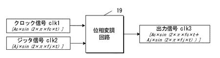
次に、図1の試験装置1のクロック信号発生回路16について説明する。このクロック信号発生回路16は、クロック信号clk1を発生し、位相変調回路19へ出力する。
Next, the clock
次に、図1の試験装置1のジッタ信号発生回路17について説明する。このジッタ信号発生回路は、ジッタ信号clk2を発生し、位相変調回路19へ出力する。
Next, the jitter
さて、図1の試験装置1のテスト信号送信回路11について説明する。
Now, the test
このテスト信号送信回路11は、テスト信号発生回路10が出力したテスト信号を、ケーブル5を介して、ディスプレイ装置3へ送信する。
The test
具体的には、テスト信号送信回路11は、上記した図1の構成からなり、詳しくは以下の通りである。
Specifically, the test
まず、図1の試験装置1のデータ送信回路18について説明する。
First, the
図4は、図1のデータ送信回路18の例示図である。図4に示すように、このデータ送信回路18は、8B10B符号化回路180、及び、送信アンプ181、を含む。
FIG. 4 is an exemplary diagram of the
8B10B符号化回路180は、図1のテストパターン発生回路15が出力した8ビットのデータ(PNパターン、テスト用映像データ)に対して、符号化を施し、2ビットの冗長ビット含む10ビットの冗長符号(以下、「8B10B符号」、と呼ぶ。)を作成する。この場合の符号化のアルゴリズムは、DVI規格書に示されている。
The 8B10B encoding circuit 180 encodes the 8-bit data (PN pattern, test video data) output from the test
送信アンプ181は、8B10B符号化回路180が発生した8B10B符号を増幅し、図1のケーブル5を介して、図1のディスプレイ装置3のデータ受信回路38に送信する。
The transmission amplifier 181 amplifies the 8B10B code generated by the 8B10B encoding circuit 180 and transmits the amplified 8B10B code to the data reception circuit 38 of the
図5は、図1の試験装置1のデータ送信回路18他の例示図である。図5に示すように、このデータ送信回路18は、送信アンプ181を含む。
FIG. 5 is a diagram illustrating another example of the
送信アンプ181は、図1のテストパターン発生回路15が出力したデータ(PNパターン、テスト用映像データ)を増幅し、図1のケーブル5を介して、図1のディスプレイ装置3のデータ受信回路38に送信する。
The transmission amplifier 181 amplifies the data (PN pattern, test video data) output from the test
DVI規格書に従う必要のない場合は、データ送信回路18として、図5のものを用いることができる。
When it is not necessary to comply with the DVI standard, the
次に、図1の試験装置1の位相変調回路19について説明する。
Next, the
図6は、位相変調回路19の例示図である。図6に示すように、この位相変調回路19は、図1のクロック信号発生回路16が出力したクロック信号clk1と、図1のジッタ信号発生回路17が出力したジッタ信号clk2と、を入力する。
FIG. 6 is an exemplary diagram of the
そして、位相変調回路19は、テスト信号としての出力信号clk3を、図1の試験装置1のテストパターン発生回路15に出力するとともに、図1のケーブル5を介して、図1のディスプレイ装置3のPLL回路39に送信する。
Then, the
ここで、入力されるジッタ信号clk2が「0」でない場合は、出力信号clk3は、ジッタを含むクロック信号である。 If the input jitter signal clk2 is not “0”, the output signal clk3 is a clock signal including jitter.
一方、入力されるジッタ信号clk2が「0」の場合、即ち、ジッタ信号clk2における「Aj」及び「fj」が「0」の場合は、出力信号clk3は、ジッタを含まないクロック信号である。 On the other hand, when the input jitter signal clk2 is “0”, that is, when “Aj” and “fj” in the jitter signal clk2 are “0”, the output signal clk3 is a clock signal that does not include jitter.
なお、上記した図3のPNパターン発生回路150は、位相変調回路19が出力するジッタを含むクロック信号clk3に同期して、PNパターンを図1の試験装置1のデータ送信回路18へ出力する。
3 outputs the PN pattern to the
また、図3のテスト用映像データ発生回路153は、位相変調回路19が出力するジッタを含まないクロック信号clk3に同期して、テスト用映像データを図1の試験装置1のデータ送信回路18へ出力する。
Also, the test video data generation circuit 153 in FIG. 3 synchronizes with the clock signal clk3 output from the
さて、図1の試験装置1の制御回路12について説明する。
Now, the
この制御回路12は、試験装置1の各回路を制御する。この点は、後で、試験全体の流れを説明する中で適宜説明する。
The
さて、図1の試験装置1のコントロール信号送信回路13及びコントロール信号受信回路14について説明する。
Now, the control
コントロール信号送信回路13は、制御回路12の命令を受けて、試験に係わるコントロール信号を、ケーブル5を介して、ディスプレイ装置3のコントロール信号受信回路32へ送信する。この点は、後で、試験全体の流れを説明する中で適宜説明する。
The control
コントロール信号受信回路14は、ディスプレイ装置3のコントロール信号送信回路33が送信した試験に係わるコントロール信号を、ケーブル5を介して受信する。この点は、後で、試験全体の流れを説明する中で適宜説明する。
The control
さて、図1のディスプレイ装置3の受信回路30について説明する。
Now, the receiving circuit 30 of the
この受信回路30は、通常モードにおいて、図2の映像データ送信装置6が送信した映像データを受信し、ディスプレイ装置3の表示ユニット31へ出力する。
The reception circuit 30 receives the video data transmitted by the video
一方、受信回路30は、試験モードにおいて、図1の試験装置1が送信したテスト信号を受信する。
On the other hand, the receiving circuit 30 receives the test signal transmitted by the
具体的には、受信回路30は、上記した図1の構成からなり、詳しくは以下の通りである。 Specifically, the receiving circuit 30 has the configuration shown in FIG. 1 described above, and details are as follows.
まず、図1のディスプレイ装置3のデータ受信に係わる回路34について説明する。このデータ受信に係わる回路34は、試験モードで、図1の試験装置1のテスト信号送信回路11が送信したテスト信号を受信する。
First, the circuit 34 related to data reception of the
一方、このデータ受信に係わる回路34は、通常モードで、図2の映像データ送信装置6が送信した映像データを受信する。
On the other hand, the circuit 34 related to this data reception receives the video data transmitted by the video
次に、図1のディスプレイ装置3の検査回路35について説明する。この検査回路35は、試験モードで、データ受信に係わる回路34を検査し、検査情報を生成して、検査結果画像生成回路37へ出力する。
Next, the inspection circuit 35 of the
次に、図1のディスプレイ装置3の検査結果画像生成回路37について説明する。この検査結果画像生成回路37は、試験モードで、検査回路35が生成した検査情報を入力する。
Next, the inspection result
そして、検査結果画像生成回路37は、入力された検査情報を表す画像データを生成する。
Then, the inspection result
以下、検査情報を表す画像データを「検査結果画像データ」と呼ぶこともある。また、検査情報を表す画像を「検査結果画像」と呼ぶこともある。 Hereinafter, the image data representing the inspection information may be referred to as “inspection result image data”. An image representing the inspection information may be referred to as an “inspection result image”.
次に、図1のディスプレイ装置3の表示切り替え回路36について説明する。この表示切り替え回路36は、通常モードでは、データ受信回路38が受信した映像データを表示ユニット31へ出力する。
Next, the display switching circuit 36 of the
一方、表示切り替え回路36は、試験モードにおいて、データ受信回路38が受信したテスト信号(PNパターン)に、検査結果画像生成回路37が生成した検査結果画像データを重畳して、表示ユニット31へ出力する。
On the other hand, the display switching circuit 36 superimposes the test result image data generated by the test result
また、表示切り替え回路36は、試験モードにおいて、データ受信回路38が受信したテスト信号(テスト用映像データ)に、検査結果画像生成回路37が生成した検査結果画像データを重畳して、表示ユニット31へ出力する。
In the test mode, the display switching circuit 36 superimposes the test result image data generated by the test result
表示切り替え回路36は、通常モード(重畳なし)と、試験モード(重畳あり)とで、動作が異なる。このような動作の切り替えは、コントロール信号受信回路32が、試験装置1からのコントロール信号を受けて、表示切り替え回路36へ出力する表示切り替え信号に従って行われる。
The operation of the display switching circuit 36 differs between the normal mode (without superimposition) and the test mode (with superimposition). Such switching of operation is performed in accordance with a display switching signal output from the control
次に、図1のディスプレイ装置3のコントロール信号受信回路32及びコントロール信号送信回路33について説明する。
Next, the control
コントロール信号受信回路32は、試験モードで、試験装置1のコントロール信号送信回路13がケーブル5を介して送信した試験に係わるコントロール信号を受信する。この点は、後で、試験全体の流れを説明する中で適宜説明する。
The control
一方、コントロール信号受信回路32は、試験に係わるコントロール信号を受信するための部材8(例えば、受信回路30が集積回路で構成されている場合は、試験に係わるコントロール信号を受信するためのピン)を利用して、通常モードにおいて、図2の映像データ送信装置6のコントロール信号送信回路63がケーブル5を介して送信したコントロール信号を受信する。
On the other hand, the control
コントロール信号送信回路33は、試験モードにおいて、試験装置1のコントロール信号受信回路14へケーブル5を介して試験に係わるコントロール信号を送信する。この点は、後で、試験全体の流れを説明する中で適宜説明する。
The control signal transmission circuit 33 transmits a control signal related to the test via the
一方、コントロール信号送信回路33は、試験に係わるコントロール信号を送信するための部材9(例えば、受信回路30が集積回路で構成されている場合は、試験に係わるコントロール信号を送信するためのピン)を利用して、通常モードにおいて、図2の映像データ送信装置6のコントロール信号受信回路64へケーブル5を介してコントロール信号を送信する。
On the other hand, the control signal transmission circuit 33 is a
さて、次に、データ受信に係わる回路34の詳細を説明する。このデータ受信に係わる回路34は、図1に示した構成からなり、次の通りである。 Next, details of the circuit 34 relating to data reception will be described. The circuit 34 related to this data reception has the configuration shown in FIG. 1 and is as follows.
まず、図1のPLL回路39について説明する。このPLL回路39は、試験モードにおいて、試験装置1の位相変調回路19がケーブル5を介して送信したクロック信号clk3に同期したタイミング信号を生成する。
First, the PLL circuit 39 in FIG. 1 will be described. The PLL circuit 39 generates a timing signal synchronized with the clock signal clk3 transmitted via the
そして、このタイミング信号を、データ受信回路38と、誤動作情報生成回路41と、に出力する。 Then, this timing signal is output to the data receiving circuit 38 and the malfunction information generating circuit 41.
一方、このPLL回路39は、通常モードにおいて、図2の映像データ送信装置6のクロック信号発生回路61がケーブル5を介して送信したクロック信号に同期したタイミング信号を生成し、データ受信回路38へ出力する。
On the other hand, the PLL circuit 39 generates a timing signal synchronized with the clock signal transmitted via the
次に、図1のデータ受信回路38について説明する。このデータ受信回路38は、試験モードにおいて、PLL回路39が出力したタイミング信号に同期して、試験装置1のデータ送信回路18が送信したテスト信号を取り込む。
Next, the data receiving circuit 38 in FIG. 1 will be described. The data receiving circuit 38 takes in the test signal transmitted from the
そして、取り込んだテスト信号を、表示切り替え回路36と、誤り情報生成回路40と、に出力する。
Then, the captured test signal is output to the display switching circuit 36 and the error
一方、通常モードにおいて、データ受信回路38は、図2の映像データ送信装置6のデータ送信回路62が送信した映像データを、PLL回路39が出力するタイミング信号に同期して取り込み、表示切り替え回路36へ出力する。
On the other hand, in the normal mode, the data reception circuit 38 takes in the video data transmitted from the
さて、次に、図1の検査回路35の詳細を説明する。この検査回路35は、図1に示した構成からなり、次の通りである。 Next, details of the inspection circuit 35 of FIG. 1 will be described. The inspection circuit 35 has the configuration shown in FIG. 1 and is as follows.
まず、誤り情報生成回路40について説明する。この誤り情報生成回路40は、試験モードにおいて、データ受信回路38が受信したテスト信号(PNパターン)について、データの誤り情報を生成し、検査情報として、検査結果画像生成回路37へ出力する。
First, the error
以下では、データの誤り情報として、「データ誤り率(ビット誤り率)」を生成する場合を例に挙げて説明する。 Hereinafter, a case where a “data error rate (bit error rate)” is generated as data error information will be described as an example.
図7は、図1のディスプレイ装置3のデータ受信回路38及び誤り情報生成回路40の例示図である。
FIG. 7 is an exemplary diagram of the data reception circuit 38 and the error
図7に示すように、このデータ受信回路38は、受信アンプ380、及び、8B10B復号回路381、を含む。
As shown in FIG. 7, the data receiving circuit 38 includes a receiving
この誤り情報生成回路40は、PNパターン発生回路400、データ比較回路401、カウンタ402、及び、割り算回路403、を含む。
The error
受信アンプ380は、図4のDVI規格書に従ったデータ送信回路18、又は、図2の映像データ送信装置6のデータ送信回路62、が送信した8B10B符号を受信し増幅して、8B10B復号回路381へ出力する。
The
8B10B復号回路381は、入力された8B10B符号を、元の8ビットのデータに復号して、図1の表示切り替え回路36へ出力する。この復号化のアルゴリズムは、DVI規格書に示されている。 The 8B10B decoding circuit 381 decodes the input 8B10B code into the original 8-bit data and outputs it to the display switching circuit 36 in FIG. The decoding algorithm is shown in the DVI standard.
試験モードでは、この復号された8ビットのデータは、図7のデータ比較回路401へも出力される。試験モードでは、試験装置1から、PNパターン発生回路150(図3)が発生したPNパターンが送信されるため、この復号された8ビットのデータは、PNパターンである。
In the test mode, the decoded 8-bit data is also output to the
図7のPNパターン発生回路400は、試験装置1のPNパターン発生回路150(図3)が発生したPNパターンと同じPNパターンを発生する。
The PN
データ比較回路401は、PNパターン発生回路400が発生したPNパターンと、8B10B復号回路381が出力したPNパターンと、を比較し、一致していないビットを検出したときは、不一致信号をカウンタ402に出力する。
The
カウンタ402は、この不一致信号をカウントし、カウント数を表す情報を、割り算回路403へ出力する。
The
割り算回路403は、このカウント数を検査ビット数で割ることにより、データ誤り率(ビット誤り率)を算出する。
The
この場合の検査ビット数は、検査フローのループ1回当たりのビット数、である。この点は、後述する試験全体の流れの説明の中で明らかになる。 The number of test bits in this case is the number of bits per loop of the test flow. This point will become clear in the description of the overall flow of the test described later.
以上のようにして算出したデータ誤り率を表す情報は、検査情報として、図1の検査結果画像生成回路37へ出力される。
Information representing the data error rate calculated as described above is output to the inspection result
図8は、図1のディスプレイ装置3のデータ受信回路38及び誤り情報生成回路40の他の例示図である。なお、図8において、図7と同様の部分については、同一の符号を付している。
FIG. 8 is another exemplary diagram of the data reception circuit 38 and the error
図8に示すように、このデータ受信回路38は、受信アンプ380を含む。
As shown in FIG. 8, the data receiving circuit 38 includes a receiving
この誤り情報生成回路40は、PNパターン発生回路400、データ比較回路401、カウンタ402、及び、割り算回路403、を含む。
The error
受信アンプ380は、図5の一般的なデータ送信回路18、又は、図2の映像データ送信装置6のデータ送信回路62、が送信したデータを受信し、増幅して、図1の表示切り替え回路36へ出力する。
The
試験モードでは、この増幅されたデータは、図8のデータ比較回路401へも出力される。試験モードでは、試験装置1から、PNパターン発生回路150(図3)が発生したPNパターンが送信されるため、この増幅されたデータは、PNパターンである。
In the test mode, the amplified data is also output to the
図8の誤り情報生成回路40は、図7の誤り情報生成回路40と同じである。
The error
次に、図1の誤動作情報生成回路41について説明する。誤動作情報生成回路41は、試験モードにおいて、PLL回路39がジッタを含むクロック信号clk3を基に生成するタイミング信号を受け取って、PLL回路39の誤動作情報を生成し、検査情報として、検査結果画像生成回路37へ出力する。
Next, the malfunction information generation circuit 41 of FIG. 1 will be described. In the test mode, the malfunction information generation circuit 41 receives a timing signal generated by the PLL circuit 39 based on the clock signal clk3 including jitter, generates malfunction information of the PLL circuit 39, and generates an inspection result image as inspection information. Output to the
以下、誤動作情報として、PLL回路のロックアウト信号を生成する場合を例に挙げて、詳しく説明する。 Hereinafter, a case where a lockout signal of a PLL circuit is generated as malfunction information will be described in detail.
ここで、PLL回路のロックアウトについて一般的に説明する。PLL回路は、入力クロックに同期した出力クロック(タイミング信号)を生成する。ロックアウトとは、PLL回路が、入力クロックに同期した出力クロック(タイミング信号)を生成できず、位相が一定でない状態である。 Here, the lockout of the PLL circuit will be generally described. The PLL circuit generates an output clock (timing signal) synchronized with the input clock. The lockout is a state in which the PLL circuit cannot generate an output clock (timing signal) synchronized with the input clock and the phase is not constant.
なお、PLL回路が入力クロックに同期した出力クロック(タイミング信号)を生成しているときは、PLL回路が「ロック」されているといい、ロックがはずれた状態が、「ロックアウト」である。 When the PLL circuit generates an output clock (timing signal) synchronized with the input clock, the PLL circuit is said to be “locked”, and the unlocked state is “lockout”.
さて、本実施の形態では、PLL回路39が、試験装置1の位相変調回路19が送信したジッタを含むクロック信号clk3に同期したタイミング信号を生成できず、そのタイミング信号の位相が一定でなくなったときに、誤動作情報生成回路41は、ロックアウト信号を、検査情報として、検査結果画像生成回路37へ出力する。
In the present embodiment, the PLL circuit 39 cannot generate the timing signal synchronized with the clock signal clk3 including the jitter transmitted by the
なお、PLL回路のロックアウトを検出する装置は、例えば、特開平7−170179号公報に開示されており、本実施の形態でも、この装置を、誤動作情報生成回路41として使用できる。 A device for detecting the lockout of the PLL circuit is disclosed in, for example, Japanese Patent Laid-Open No. 7-170179, and this device can also be used as the malfunction information generation circuit 41 in this embodiment.
さて、検査結果画像生成回路37は、誤動作情報生成回路41から入力されるロックアウト信号を基に、PLL回路39のロックアウトの有無を表す情報を生成する。
The inspection result
そして、検査結果画像生成回路37は、データ誤り率と、ロックアウトの有無と、を表す画像データ(検査結果画像データ)を生成する。
Then, the inspection result
さて、これまで説明してきた図1の受信回路30は、集積回路(LSI)として構成することもできる。 The receiving circuit 30 of FIG. 1 described so far can also be configured as an integrated circuit (LSI).
以下では、「部材」という語句を用いる場合があるが、受信回路30が、LSIとして構成されているときは、この「部材」とは、LSIにおける信号の入出力のための「ピン」を意味する。なお、当然のことながら、受信回路30が、LSIとして構成されているときでも、「部材」には、他の周知の端子が含まれる。 In the following, the term “member” may be used, but when the receiving circuit 30 is configured as an LSI, the “member” means a “pin” for input / output of a signal in the LSI. To do. As a matter of course, even when the receiving circuit 30 is configured as an LSI, the “member” includes other well-known terminals.
さて、図1のディスプレイ装置3の表示ユニット31について説明する。この表示ユニット31は、通常モードにおいて、表示切り替え回路36が出力した映像データを表示する。
Now, the
一方、表示ユニット31は、試験モードにおいて、表示切り替え回路36が出力した、テスト信号(PNパターン、テスト用映像データ)に検査結果画像データを重畳した画像データを表示する。
On the other hand, in the test mode, the
さて、本実施の形態による試験全体の流れを、図1及びフローチャートを用いて説明する。 Now, the entire test flow according to this embodiment will be described with reference to FIG. 1 and a flowchart.
図9は、本実施の形態における試験装置1及びディスプレイ装置3のフローチャートである。
FIG. 9 is a flowchart of the
図9に示すように、まず、ステップ1にて、試験装置1の初期化を実行する。次に、ステップ2にて、ディスプレイ装置3の検査を実行する。次に、ステップ3にて、ディスプレイ装置3の表示ユニット31に、検査結果画像データを表示する。
As shown in FIG. 9, first, in
次に、図9の各ステップにおける処理の詳細を説明する。 Next, details of processing in each step of FIG. 9 will be described.
図10は、図9のステップ1における初期化のフローチャート(初期化フロー)である。なお、図10において、左側の処理は、試験装置1の処理を示し、右側の処理は、ディスプレイ装置3の処理を示している。
FIG. 10 is a flowchart (initialization flow) of initialization in
図10に示すように、まず、ステップ10にて、試験装置1を初期化する。具体的には、次の通りである。
As shown in FIG. 10, first, in
試験装置1の制御回路12は、テストパターン発生回路15のスイッチ回路154(図3)に対して、切り替え信号を出力して、テストパターン発生回路15が、PNパターンを出力するように切り替える。また、制御回路12は、ジッタ信号発生回路17を初期化する。
The
次にステップ11にて、試験装置1がディスプレイ装置3に対して試験開始を指示する。具体的には、次の通りである。
Next, in
ディスプレイ装置3のコントロール信号受信回路32へ、試験開始を指示するコントロール信号を送信するように、試験装置1の制御回路12が、コントロール信号送信回路13に対して命令する。
The
すると、試験装置1のコントロール信号送信回路13は、試験開始を指示するコントロール信号を、ディスプレイ装置3のコントロール信号受信回路32へ送信する。
Then, the control
すると、ステップ12にて、ディスプレイ装置3のコントロール信号受信回路32は、表示切り替え信号を表示切り替え回路36に出力し、表示切り替え回路36をオンにする。
Then, in
すると、ステップ13にて、ディスプレイ装置3のコントロール信号送信回路33は、試験の準備が完了したことを通知するコントロール信号を、試験装置1のコントロール信号受信回路14へ送信する。
Then, in
これにより、ディスプレイ装置3は、試験モードに入ることになる。
As a result, the
すると、ステップ14にて、試験装置1のコントロール信号受信回路14が、試験の準備が完了したことを通知するコントロール信号を受信し、その旨を、制御回路12に、通知する。
Then, in
次に、図9のステップ2へ進む。 Next, the process proceeds to Step 2 in FIG.
図11は、図9のステップ2における検査のフローチャート(検査フロー)である。なお、図11において、左側の処理は、試験装置1の処理を示し、右側の処理は、ディスプレイ装置3の処理を示している。
FIG. 11 is a flowchart (inspection flow) of inspection in
図11に示すように、まず、ステップ20にて、試験装置1の位相変調回路19が、テストパターン発生回路15と、ディスプレイ装置3のPLL回路39と、に対して、ジッタを含むクロック信号clk3を出力する。
As shown in FIG. 11, first, in
すると、ステップ21にて、試験装置1のテストパターン発生回路15は、位相変調回路19が供給するジッタを含むクロック信号に同期して、一定ビット数のPNパターンを出力する。
Then, in step 21, the test
そして、試験装置1のデータ送信回路18が、ディスプレイ装置3のデータ受信回路38へ、PNパターンを送信する。
Then, the
一方、ステップ22にて、ディスプレイ装置3のPLL回路39は、受信したジッタを含むクロック信号clk3に同期したタイミング信号を生成する。そして、PLL回路39は、生成したタイミング信号を、データ受信回路38と、誤動作情報生成回路41と、に出力する。
On the other hand, in
すると、ステップ23にて、タイミング信号を入力した誤動作情報生成回路41は、PLL回路39がロックアウト状態になったときに、ロックアウト信号を生成し、検査情報として、検査結果画像生成回路37へ出力する。
Then, in step 23, the malfunction information generation circuit 41 to which the timing signal has been input generates a lockout signal when the PLL circuit 39 is in the lockout state, and sends it to the inspection result
一方、ステップ24にて、ディスプレイ装置3のデータ受信回路38は、PLL回路39が供給するタイミング信号に同期して、試験装置1のデータ送信回路18が送信したPNパターンを取り込む。
On the other hand, in step 24, the data reception circuit 38 of the
そして、データ受信回路38は、受信したPNパターンを、受信データとして、表示切り替え回路36と、誤り情報生成回路40と、に出力する。
Then, the data reception circuit 38 outputs the received PN pattern to the display switching circuit 36 and the error
すると、ステップ25にて、誤り情報生成回路40は、受信データのデータ誤り率を計算し、検査情報として、検査結果画像生成回路37へ出力する。
Then, in step 25, the error
次に、ステップ26にて、ディスプレイ装置3の検査結果画像生成回路37は、検査情報(ジッタ周波数、PLL回路39のロックアウトの有無、データ誤り率)を1行追加して、検査情報を表す画像データ(検査結果画像データ)を生成し、表示切り替え回路36へ出力する。
Next, in step 26, the inspection result
なお、この検査情報(ジッタ周波数、PLL回路39のロックアウトの有無、データ誤り率)は、記憶回路(図示せず)に記憶される。 This inspection information (jitter frequency, presence / absence of lockout of the PLL circuit 39, data error rate) is stored in a storage circuit (not shown).
次に、ステップ27にて、表示切り替え回路36は、データ受信回路38が出力した受信データ(PNパターン)に、検査結果画像生成回路37が出力した検査結果画像データを重畳して、表示ユニット31へ出力する。
Next, in step 27, the display switching circuit 36 superimposes the inspection result image data output from the inspection result
次に、ステップ28にて、表示ユニット31は、検査結果画像データを重畳した受信データ(PNパターン)を表示する。
Next, in step 28, the
次に、検査が完了したならば、図9のステップ3に進み、検査が完了していないならば、ステップ30へ進む(ステップ29)。 Next, if the inspection is completed, the process proceeds to step 3 in FIG. 9, and if the inspection is not completed, the process proceeds to step 30 (step 29).
ステップ30にて、試験装置1の制御回路12は、ジッタ信号発生回路17におけるジッタ周波数を変更する。そして、そのジッタ周波数で、ステップ20からステップ29の処理が実行される。
In step 30, the
図11に示した検査フローのループ1回当たりのビット数が、検査ビット数であり、図7及び図8の誤り情報生成回路40では、PNパターンの一致していないビット数を、この検査ビット数で割ることにより、データ誤り率(ビット誤り率)を計算する。
The number of bits per loop of the check flow shown in FIG. 11 is the number of check bits, and the error
さて、図9のステップ3における処理の詳細を説明する。
Details of the process in
図12は、図9のステップ3における表示のフローチャート(表示フロー)である。なお、図12において、左側の処理は、試験装置1の処理を示し、右側の処理は、ディスプレイ装置3の処理を示している。
FIG. 12 is a flowchart (display flow) of display in
図12に示すように、ステップ31にて、試験装置1の制御回路12は、ジッタ信号発生回路17に対して、ジッタ信号の発生の停止を命令する。
As shown in FIG. 12, in
すると、ジッタ信号発生回路17は、ジッタ信号clk2のジッタ振幅Ajとジッタ周波数fjと、を「0」にし、ジッタ信号clk2の発生を停止する。
Then, the jitter
すると、ステップ32にて、試験装置1の位相変調回路19が、テストパターン発生回路15と、ディスプレイ装置3のPLL回路39と、にジッタを含まないクロック信号clk3を出力する。
Then, in
ステップ33にて、試験装置1の制御回路12は、テストパターン発生回路15のスイッチ回路154(図3)に対して、切り替え信号を出力して、テストパターン発生回路15が、テスト用映像データを出力するように切り替える。
In step 33, the
すると、ステップ34にて、テストパターン発生回路15は、位相変調回路19が出力したジッタを含まないクロック信号に同期して、テスト用映像データを出力する。
Then, in step 34, the test
そして、試験装置1のデータ送信回路18が、そのテスト用映像データを、ディスプレイ装置3のデータ受信回路38へ送信する。
Then, the
一方、ステップ35にて、ディスプレイ装置3のPLL回路39は、試験装置1の位相変調回路19が送信したジッタを含まないクロック信号に同期してタイミング信号を生成する。
On the other hand, in step 35, the PLL circuit 39 of the
そして、PLL回路39は、生成したタイミング信号を、データ受信回路38へ出力する。 Then, the PLL circuit 39 outputs the generated timing signal to the data receiving circuit 38.
すると、ステップ36にて、ディスプレイ装置3のデータ受信回路38は、PLL回路39が出力したタイミング信号に同期して、試験装置1のータ送信回路18が送信したテスト用映像データを取り込む。
Then, in step 36, the data receiving circuit 38 of the
そして、データ受信回路38は、受信したテスト用映像データを、受信データとして、表示切り替え回路36へ出力する。 Then, the data reception circuit 38 outputs the received test video data to the display switching circuit 36 as reception data.
一方、ステップ37にて、ディスプレイ装置3の検査結果画像生成回路37は、記憶回路(図示せず)から、検査情報(ジッタ周波数、PLL回路39のロックアウトの有無、データ誤り率)を取得して、検査情報を表す画像データ(検査結果画像データ)を生成する。
On the other hand, in
そして、検査結果画像生成回路37は、生成した検査結果画像データを、表示切り替え回路36へ出力する。
Then, the inspection result
次に、ステップ38にて、ディスプレイ装置3の表示切り替え回路36は、データ受信回路38が出力した受信データ(テスト用映像データ)に、検査結果画像生成回路37が出力した検査結果画像データを重畳して、表示ユニット31へ出力する。
Next, in step 38, the display switching circuit 36 of the
すると、ステップ39にて、ディスプレイ装置3の表示ユニット31は、検査結果画像データを重畳したテスト用映像データを表示する。
Then, in step 39, the
次に、この表示例を示す。 Next, this display example is shown.
図13は、図12のステップ39において、ディスプレイ装置3の表示ユニット31が表示する画像データの例示図である。
FIG. 13 is a view showing an example of image data displayed on the
図13(a)は、図1のコントロール信号受信回路32からの表示切り替え信号がオンのときの表示例、図13(b)は、図1のコントロール信号受信回路32からの表示切り替え信号がオフのときの表示例、である。
13A shows a display example when the display switching signal from the control
図10のステップ12により、コントロール信号受信回路32が、表示切り替え信号をオンにして、表示切り替え回路36をオンにしている。
In
このため、図13(a)に示すように、ディスプレイ装置3の表示ユニット31には、検査結果画像データを重畳したテスト用映像データが表示される。
For this reason, as shown in FIG. 13A, the test video data on which the inspection result image data is superimposed is displayed on the
具体的には、表示ユニット31のメイン画面310にテスト用映像Aが表示され、サブ画面311に検査結果画像Bが表示される。
Specifically, the test video A is displayed on the main screen 310 of the
一方、ディスプレイ装置3のコントロール信号受信回路32が、試験装置1のコントロール信号送信回路13が送信するコントロール信号の指示を受けて、表示切り替え信号をオフにしたときは、表示切り替え回路36がオフになり、表示ユニット31には、テスト用映像データが出力される。
On the other hand, when the control
この場合は、図13(b)に示すように、表示ユニット31のメイン画面310にテスト用映像Aが表示されるだけである。
In this case, only the test video A is displayed on the main screen 310 of the
図14は、図13の表示ユニット31のサブ画面311に表示される検査結果画像Bの例示図である。
FIG. 14 is an exemplary view of an inspection result image B displayed on the sub-screen 311 of the
図14に示すように、表示ユニット31のサブ画面311には、検査結果画像として、ジッタ周波数、PLL回路のロックアウトの有無、データ誤り率(ビット誤り率)、が表示される。なお、PLL回路のロックアウトの有無の表示において、「OK」は、PLL回路がロック状態にあることを示し、「NG」は、PLL回路がロックアウト状態にあることを示している。
As shown in FIG. 14, on the sub-screen 311 of the
さて、次に、別の表示方法を説明する。 Now, another display method will be described.
図1の試験装置1の表示切り替え回路36は、テスト用映像データに検査結果画像データを重畳して、表示ユニット31へ出力したが、このような重畳をすることなく、単なるスイッチ回路として用いることができる。
The display switching circuit 36 of the
すなわち、この場合は、図10のステップ12により、コントロール信号受信回路32が、表示切り替え信号をオンにして、表示切り替え回路36をオンにしているときは、図12のステップ38にて重畳することなく、表示切り替え回路36は、検査結果画像生成回路37が出力した検査結果画像データを表示ユニット31に出力する。
That is, in this case, when the control
一方、ディスプレイ装置3のコントロール信号受信回路32が、試験装置1のコントロール信号送信回路14が送信するコントロール信号の指示を受けて、表示切り替え信号をオフにしたときは、表示切り替え回路36がオフになり、表示ユニット31には、テスト用映像データが出力される。
On the other hand, when the control
これらの点を図面を用いて説明する。 These points will be described with reference to the drawings.
図15は、図12のステップ39において、ディスプレイ装置3の表示ユニット31が表示する画像データの他の例示図である。
FIG. 15 is another exemplary view of image data displayed on the
図15(a)は、図1のコントロール信号受信回路32からの表示切り替え信号がオンのときの表示例、図15(b)は、図1のコントロール信号受信回路32からの表示切り替え信号がオフのときの表示例、である。
15A shows a display example when the display switching signal from the control
図15(a)に示すように、表示切り替え回路36を単なるスイッチ回路として用いる場合は、図12のステップ39にて、表示ユニット31のメイン画面310に、検査結果画像Bが表示される。ここで表示される検査結果画像Bは、例えば、図14のような画像である。
As shown in FIG. 15A, when the display switching circuit 36 is used as a simple switch circuit, the inspection result image B is displayed on the main screen 310 of the
一方、表示切り替え信号がオフで、表示切り替え回路36がオフのときは、図15(b)に示すように、表示ユニット31のメイン画面310に、テスト用映像Aが表示される。
On the other hand, when the display switching signal is OFF and the display switching circuit 36 is OFF, the test video A is displayed on the main screen 310 of the
さて、本実施の形態では、図1のディスプレイ装置3のデータ受信回路38に、ジッタを含むクロック信号に同期したタイミング信号を供給しているため(図11のステップ20、22)、データ誤り率を計測することで、ジッタの影響を知ることができる。なお、このデータ誤り率に影響を与える他の主なものとして、他の回路からのノイズがあり、データ誤り率には、この影響も含まれる。
In the present embodiment, since the timing signal synchronized with the clock signal including jitter is supplied to the data receiving circuit 38 of the
また、本実施の形態では、図1のディスプレイ装置3のPLL回路39にジッタを含むクロック信号を供給しているため(図11のステップ20、22)、ロックアウト信号を検出することで、PLL回路39へのジッタの影響を知ることができる。なお、PLL回路39に影響を与える他の主なものとして、他の回路からのノイズがあり、PLL回路39のロックアウトには、この影響も含まれる。
In this embodiment, since a clock signal including jitter is supplied to the PLL circuit 39 of the
さて、これまで、試験モードでの動作を説明してきたが、図2を用いて、通常モードでの動作を簡単に説明する。 The operation in the test mode has been described so far, but the operation in the normal mode will be briefly described with reference to FIG.
図2に示すように、映像データ送信装置6のコントロール信号送信回路63は、映像データを送信する旨を通知するコントロール信号を、ケーブル5を介して、ディスプレイ装置3のコントロール信号受信回路32へ送信する。
As shown in FIG. 2, the control
すると、コントロール信号受信回路32は、試験に係わるコントロール信号を受信するための部材8(例えば、受信回路30が集積回路で構成されている場合のピン)を利用して、そのコントロール信号を受信する。
Then, the control
すると、ディスプレイ装置3のコントロール信号送信回路33は、試験に係わるコントロール信号を送信するための部材9(例えば、受信回路30が集積回路で構成されている場合のピン)を利用して、ディスプレイ装置3の解像度などの表示制御情報を、ケーブル5を介して、映像データ送信装置6のコントロール信号受信回路64に送信する。
Then, the control signal transmission circuit 33 of the
映像データ送信装置6のクロック信号発生回路61は、クロック信号を発生し、映像生成回路60と、ディスプレイ装置3のPLL回路39と、に送信する。
The clock
映像生成回路60は、クロック信号発生回路61が供給するクロック信号に同期して、映像データを出力する。
The
そして、データ送信回路62は、映像生成回路60が出力した映像データを、ケーブル5を介して、ディスプレイ装置3のデータ受信回路38へ送信する。
Then, the
ディスプレイ装置3のデータ受信回路38は、PLL回路39がクロック信号に同期して生成したタイミング信号に同期して、映像データを取り込む。
The data receiving circuit 38 of the
データ受信回路38は、取り込んだ映像データを表示切り替え回路36に出力する。 The data receiving circuit 38 outputs the captured video data to the display switching circuit 36.
このとき、表示切り替え回路36はオフになっており、映像データは、表示ユニット31へ出力され、表示される。
At this time, the display switching circuit 36 is off, and the video data is output to the
さて、これまで説明してきたように、本実施の形態におけるディスプレイ装置3については、次のことが言える。
As described above, the following can be said about the
本実施の形態では、図1のディスプレイ装置3の内部に検査回路35を設けているため、ディスプレイ装置3の内部で、データ受信に係わる回路34が検査され、検査情報(データ誤り率、ロックアウト信号)が生成される。
In the present embodiment, since the inspection circuit 35 is provided in the
そして、検査結果画像生成回路37は、その検査情報を表す画像データ(検査結果画像データ)を生成し、この検査結果画像データが、ディスプレイ装置3が備える表示ユニット31に表示される(図13から図15)。
Then, the inspection result
その結果、ディスプレイ装置3の組立後に、しかも、ディスプレイ装置3の分解をすることなく、検査が可能となって、ディスプレイ装置3の内部のノイズ環境を変えることなく、ディスプレイ装置3の内部のデータ受信に係わる回路34の試験を簡易に実行できる。
As a result, after the
また、検査結果画像データは、ディスプレイ装置3が備える表示ユニット31に表示されるため、検査結果画像データを出力する端子を、ディスプレイ装置3の外部に新たに設けることが不要になる。
Further, since the inspection result image data is displayed on the
また、ディスプレイ装置3のコントロール信号受信回路32は、試験装置1からの試験に係わるコントロール信号の受信を行うとともに、その試験に係わるコントロール信号を受信するための部材8を介して、その試験に係わるコントロール信号とは別の外部からの信号を受信でき、かつ、処理できる。
Further, the control
そして、コントロール信号受信回路32が、試験に係わるコントロール信号として、試験装置1から試験開始を指示するコントロール信号を受信した後に、ディスプレイ装置3は試験モードに移行する。
Then, after the control
このように、ディスプレイ装置3のコントロール信号受信回路32は、試験に係わるコントロール信号とは別の外部からの信号を受信でき、かつ、処理できるため、外部から通常モードに戻ることを指示するコントロール信号を、コントロール信号受信回路32に送信することにより、通常モードに移行でき、また、外部の試験装置1からコントロール信号受信回路32へ試験開始を指示するコントロール信号を送信するだけで試験モードへ移行することができる。
Thus, since the control
つまり、ディスプレイ装置3の外部からのコントロール信号だけで、モードの切り替えを実行できる。
That is, the mode can be switched only by a control signal from the outside of the
その結果、ディスプレイ装置3の内部のデータ受信に係わる回路34の試験をより簡易に実行できる。
As a result, the test of the circuit 34 related to data reception inside the
また、ディスプレイ装置3のコントロール信号受信回路32は、試験に係わるコントロール信号とは別の外部からの信号を受信でき、かつ、処理できるため、外部の映像データ送信装置6が送信する信号の受信及び処理が可能である。
Further, since the control
このため、通常モードに移行した後に、外部の映像データ送信装置6は、コントロール信号受信回路32に対して、必要に応じて信号を送信できる。
Therefore, after shifting to the normal mode, the external video
このように、試験モードだけでなく、通常モードでも使用できるコントロール信号受信回路32を設けている。
Thus, the control
しかも、このコントロール信号受信回路32は、試験モードと通常モードとで、外部からの信号を受信する際、共通の部材8を用いている。
Moreover, the control
その結果、ディスプレイ装置3において、試験に係わるコントロール信号の受信を行うためだけの部材を新たに設けることが不要となり、実装面積の増加及び部材互換性喪失(他のLSIとのピン互換性喪失)といった不都合を回避できる。
As a result, it is not necessary to provide a new member only for receiving a control signal related to the test in the
また、ディスプレイ装置3のコントロール信号送信回路33は、試験に係わるコントロール信号の送信を行うとともに、その試験に係わるコントロール信号を送信するための部材9を介して、その試験に係わるコントロール信号とは別の信号を外部へ送信できる。
Further, the control signal transmission circuit 33 of the
これにより、コントロール信号送信回路33は、試験に係わるコントロール信号を外部に送信するための部材9を介して、外部の映像データ送信装置6への信号の送信が可能となる。
As a result, the control signal transmission circuit 33 can transmit a signal to the external video
このため、通常モードに移行した後に、コントロール信号送信回路33は、外部の映像データ送信装置6に対して、必要に応じて信号を送信できる。
Therefore, after shifting to the normal mode, the control signal transmission circuit 33 can transmit a signal to the external video
このように、試験モードだけでなく、通常モードでも使用できるコントロール信号送信回路33を設けている。 Thus, the control signal transmission circuit 33 that can be used not only in the test mode but also in the normal mode is provided.
しかも、コントロール信号送信回路33は、試験モードと通常モードとで、外部へ信号を送信する際、共通の部材9を用いている。
Moreover, the control signal transmission circuit 33 uses the
その結果、ディスプレイ装置3において、試験に係わる信号の送信を行うためだけの部材を新たに設けることが不要となり、実装面積の増加及び部材互換性喪失(他のLSIとのピン互換性喪失)といった不都合を回避できる。
As a result, it is not necessary to provide a new member only for transmitting a signal related to the test in the
また、ディスプレイ装置3の表示切り替え回路36は、試験モードにおいて、データ受信回路38が入力したテスト信号(テスト用映像データ)に、検査結果画像生成回路37が生成した検査結果画像データを重畳して、表示ユニット31へ出力する。
In the test mode, the display switching circuit 36 of the
このため、ディスプレイ装置3の表示ユニット31において、データ受信に係わる回路34の検査結果の確認とともに、テスト信号として、外部からテスト用映像データを送信することで、テスト用映像データを目視検査できる(図13(a))。
For this reason, in the
また、表示切り替え回路36は、モードに応じて、映像データ、又は、検査結果画像データを重畳したテスト用映像データ、のいずれか一方を表示ユニット31へ出力するので、映像データを表示ユニット31へ出力するための部材と、検査結果画像データを重畳したテスト用映像データを表示ユニット31へ出力するための部材と、を共通にすることができる。
Further, the display switching circuit 36 outputs either the video data or the test video data on which the inspection result image data is superimposed to the
その結果、表示切り替え回路36から表示ユニット31へ、検査結果画像データを重畳したテスト用映像データを出力するときだけ使用する部材を新たに設けることが不要となり、実装面積の増加及び部材互換性喪失(他のLSIとのピン互換性喪失)といった不都合を回避できる。
As a result, it is not necessary to newly provide a member to be used only when outputting test video data on which the inspection result image data is superimposed from the display switching circuit 36 to the
また、表示切り替え回路36を単なるスイッチ回路として用いるときは、表示切り替え回路36は、通常モードにおいて、データ受信回路38から映像データを受け取って、表示ユニット31へ出力し、試験モードにおいて、検査結果画像生成回路37が生成した検査結果画像データを受け取って、表示ユニット31へ出力する。
When the display switching circuit 36 is used as a mere switch circuit, the display switching circuit 36 receives video data from the data receiving circuit 38 in the normal mode and outputs it to the
このため、ディスプレイ装置3の表示ユニット31において、データ受信に係わる回路34の検査結果の確認ができる(図15(a))。
For this reason, in the
また、表示切り替え回路36を単なるスイッチ回路とするときは、重畳を行うための機能が不要となるため、表示切り替え回路36を単純化できる。 Further, when the display switching circuit 36 is a simple switch circuit, the display switching circuit 36 can be simplified because the function for superimposing is not necessary.
また、単なるスイッチ回路としての表示切り替え回路36は、モードに応じて、映像データ、又は、検査結果画像生成回路37が生成した検査結果画像データ、のいずれか一方を表示ユニット31へ出力するので、映像データを表示ユニット31へ出力するための部材と、検査結果画像生成回路37が生成した検査結果画像データを表示ユニット31へ出力するための部材と、を共通にすることができる。
Further, the display switching circuit 36 as a simple switch circuit outputs either video data or the inspection result image data generated by the inspection result
その結果、単なるスイッチ回路としての表示切り替え回路36から表示ユニット31へ、検査結果画像データを出力するときだけ使用する部材を新たに設けることが不要となり、実装面積の増加及び部材互換性喪失(他のLSIとのピン互換性喪失)といった不都合を回避できる。
As a result, it is not necessary to newly provide a member to be used only when outputting the inspection result image data from the display switching circuit 36 as a mere switch circuit to the
また、単なるスイッチ回路としての表示切り替え回路36は、試験モードにおいて、コントロール信号受信回路32が受信した表示の切り替えを指示するコントロール信号に従って、検査結果画像生成回路37が生成した検査結果画像データを受け取って、表示ユニット31へ出力し、又は、テスト信号としてのテスト用映像データを受け取って、表示ユニット31へ出力する。
Further, the display switching circuit 36 as a simple switch circuit receives the inspection result image data generated by the inspection result
このように、単なるスイッチ回路としての表示切り替え回路36が、試験モードにおいて、コントロール信号に従って、検査結果画像データ、又は、テスト用映像データ、のうちのいずれか1つを表示ユニット31へ出力するので、検査結果画像データを表示ユニット31へ出力するための部材と、テスト用映像データを表示ユニット31へ出力するための部材と、を共通にすることができる。
In this way, the display switching circuit 36 as a simple switch circuit outputs either one of the inspection result image data or the test video data to the
その結果、単なるスイッチ回路としての表示切り替え回路36から表示ユニット31へ、試験モードにおけるデータ(検査結果画像データ、テスト用映像データ)を出力するときだけ使用する部材を新たに設けることが不要となり、実装面積の増加及び部材互換性喪失(他のLSIとのピン互換性喪失)といった不都合を回避できる。
As a result, it is not necessary to newly provide a member that is used only when outputting data (inspection result image data, test video data) in the test mode from the display switching circuit 36 as a simple switch circuit to the
また、外部からコントロール信号を送信するだけで、ディスプレイ装置3の表示ユニット31において、テスト用映像データを目視検査できる(図13(b)、図15(b))。
In addition, the test video data can be visually inspected in the
また、ディスプレイ装置3のデータ受信回路38は、通常モードにおいて、映像データを受信し、試験モードにおいて、テスト信号としてのPNパターンを受信する。
The data receiving circuit 38 of the
そして、ディスプレイ装置3の誤り情報生成回路40は、試験モードにおいて、データ受信回路38が受信したPNパターンについてのデータ誤り率を生成する。そして、このデータ誤り率は、表示ユニット31に表示される(図14)。
Then, the error
このため、ディスプレイ装置3の組立後に、しかも、ディスプレイ装置3の分解をすることなく、検査が可能となって、ディスプレイ装置3の内部のノイズ環境を変えることなく、ディスプレイ装置3の内部のデータ受信回路38の試験(データ誤り率の測定)を簡易に実行できる。
For this reason, after the
また、PLL回路39は、通常モードにおいて、クロック信号を受信し、試験モードにおいて、テスト信号としてのジッタを含むクロック信号を受信し、それらに同期したタイミング信号を発生する。 The PLL circuit 39 receives a clock signal in the normal mode, receives a clock signal including jitter as a test signal in the test mode, and generates a timing signal synchronized therewith.
そして、誤動作情報生成回路41は、試験モードにおいて、PLL回路39がロックアウトしたときに、ロックアウト信号を生成する。このロックアウトの有無は、表示ユニット31に表示される(図14)。 Then, the malfunction information generation circuit 41 generates a lockout signal when the PLL circuit 39 is locked out in the test mode. The presence or absence of this lockout is displayed on the display unit 31 (FIG. 14).
このため、ディスプレイ装置3の組立後に、しかも、ディスプレイ装置3の分解をすることなく、検査が可能となって、ディスプレイ装置3の内部のノイズ環境を変えることなく、ディスプレイ装置3の内部のPLL回路39の試験(ロックアウト信号の検出)を簡易に実行できる。
For this reason, after the
また、PLL回路39及びデータ受信回路38の双方が検査されるため、ディスプレイ装置3の誤動作の原因が、PLL回路39にあるのか、あるいは、他の伝送劣化要因にあるのか、を判断でき、ディスプレイ装置3の誤動作の原因を極力具体的に特定できる。
Further, since both the PLL circuit 39 and the data receiving circuit 38 are inspected, it is possible to determine whether the malfunction of the
また、ディスプレイ装置3のデータ受信回路38は、通常モードにおいて、クロック信号を基にしたタイミング信号に同期して、映像データを受信し、試験モードにおいて、ジッタを含むクロック信号を基にしたタイミング信号に同期して、テスト信号としてのPNパターンを受信する。
The data receiving circuit 38 of the
このようなタイミング信号に同期して受信したPNパターンについてのデータ誤り率を算出することで、ジッタの影響について知見を得ることができる。 By calculating the data error rate for a PN pattern received in synchronization with such a timing signal, knowledge about the influence of jitter can be obtained.
また、本実施の形態では、検査回路35が、データ受信に係わる回路34を検査し、検査情報を生成して、この検査情報を表す画像データ(検査結果画像データ)が表示ユニット31に表示される。
In the present embodiment, the inspection circuit 35 inspects the circuit 34 related to data reception, generates inspection information, and image data (inspection result image data) representing the inspection information is displayed on the
このため、人間が目視検査のみを行う場合に比較して、客観的で、精度の高い検査結果を得ることができる。 For this reason, it is possible to obtain an objective and highly accurate inspection result as compared with a case where a human performs only a visual inspection.
さて、これまで説明してきたように、本実施の形態における試験装置1については、次のことが言える。
As described above, the following can be said about the
本実施の形態では、試験装置1のコントロール信号送信回路13は、制御回路12からの命令を受けて、ディスプレイ装置3に対して、試験開始を指示するコントロール信号を送信する。
In the present embodiment, the control
このように、ディスプレイ装置3へコントロール信号を送信するだけで、テスト信号を受信するディスプレイ装置3を、試験が開始できる状態に簡易にすることができる。
Thus, the
また、試験装置1の制御回路12は、テスト信号発生回路10のジッタ信号発生回路17に対して、テスト条件としてのジッタ周波数を指示する。
Further, the
このため、従来、手動でジッタ周波数の設定を行っていたときと比較して、ジッタ周波数の設定のための手間を軽減できる。 For this reason, it is possible to reduce time and effort for setting the jitter frequency compared to the case where the jitter frequency is manually set conventionally.
また、試験装置1のテストパターン発生回路15は、テスト信号としてのPNパターンを発生する。そして、このPNパターンは、ディスプレイ装置3に送信される。
In addition, the test
このため、ディスプレイ装置3において、データ受信回路38が受信したPNパターンについてのデータ誤り率を算出できる。
For this reason, in the
また、試験装置1の位相変調回路19は、クロック信号clk1にジッタ信号clk2を重畳して、ジッタを含むクロック信号clk3を生成し、テスト信号としてのジッタを含むクロック信号clk3をディスプレイ装置3のPLL回路39へ送信する。
Further, the
このため、ディスプレイ装置3において、PLL回路39のロックアウト信号を検出することで、ジッタが及ぼすPLL回路39への影響を知ることができる。
Therefore, by detecting the lockout signal of the PLL circuit 39 in the
また、試験装置1のテストパターン発生回路15は、位相変調回路19が生成したジッタを含むクロック信号に同期して、データ送信回路18へPNパターンを出力する。
The test
このため、ディスプレイ装置3において、データ受信回路38が受信したPNパターンのデータ誤り率に対するジッタの影響を知ることができる。
For this reason, the
また、試験装置1は、テスト信号(PNパターン、テスト用映像データ、ジッタを含むクロック信号clk3)を、ケーブル5を介して、ディスプレイ装置3に送信する。
In addition, the
このため、ディスプレイ装置3のデータ受信に係わる回路34(データ受信回路38、PLL回路39)の検査において、ケーブルの影響について知見を得ることができる。
For this reason, in the inspection of the circuit 34 (data reception circuit 38, PLL circuit 39) related to data reception of the
なお、試験装置1を、ケーブル5を介することなく、ディスプレイ装置3に直結して、試験を実行することもできる。
Note that the test can be executed by directly connecting the
また、ディスプレイ装置3の表示ユニット31において、テスト用映像データの目視検査を行う必要がないときは、図3のテスト用映像データ発生回路153は、省略できる。
When the
この場合は、図1のディスプレイ装置3の表示切り替え回路36は、単なるスイッチ回路として使用されることになる。
In this case, the display switching circuit 36 of the
(実施の形態2)
本実施の形態では、実施の形態1と異なり、試験装置1が、ディスプレイ装置から検査情報を受信して、検査結果画像データを生成し、そして、ディスプレイ装置に送信する。以下、詳しく説明する。
(Embodiment 2)
In the present embodiment, unlike the first embodiment, the
図16は、本発明の実施の形態2における試験装置1及びディスプレイ装置のブロック図である。なお、図16において、図1と同様の部分については、同一の符号を付して、適宜説明を省略する。
FIG. 16 is a block diagram of the
図16に示すように、試験装置8と、ディスプレイ装置7とは、ケーブル5で接続される。
As shown in FIG. 16, the
試験装置8は、テスト信号発生回路80、テスト信号送信回路11、制御回路12、コントロール信号送信回路13、コントロール信号受信回路14、検査結果画像生成回路82、及び、検査情報記憶回路83、を具備する。
The
テスト信号発生回路80は、テストパターン発生回路15、クロック信号発生回路16、ジッタ信号発生回路17、及び、重畳回路81、を含む。
The test signal generation circuit 80 includes a test
テスト信号送信回路11は、データ送信回路18、及び、位相変調回路19、を含む。
The test
ディスプレイ装置7は、受信回路70、及び、表示ユニット31、を具備する。
The display device 7 includes a receiving circuit 70 and a
受信回路70は、データ受信に係わる回路34、検査回路35、コントロール信号受信回路32、及び、コントロール信号送信回路33、を含む。
The reception circuit 70 includes a circuit 34 related to data reception, an inspection circuit 35, a control
データ受信に係わる回路34は、データ受信回路38、及び、PLL回路(位相同期ループ回路)39、を含む。 The circuit 34 related to data reception includes a data receiving circuit 38 and a PLL circuit (phase locked loop circuit) 39.
検査回路35は、誤り情報生成回路40、及び、誤動作情報生成回路41、を含む。
The inspection circuit 35 includes an error
さて、受信回路70は、図1の受信回路30と同様に、集積回路(LSI)として構成することもできる。 The receiving circuit 70 can also be configured as an integrated circuit (LSI), similar to the receiving circuit 30 of FIG.
以下では、「部材」という語句を用いる場合があるが、受信回路70が、LSIとして構成されているときは、この「部材」とは、LSIにおける信号の入出力のための「ピン」を意味する。なお、当然のことながら、受信回路701が、LSIとして構成されているときでも、「部材」には、他の周知の端子が含まれる。 In the following, the term “member” may be used, but when the receiving circuit 70 is configured as an LSI, the “member” means a “pin” for input / output of a signal in the LSI. To do. As a matter of course, even when the receiving circuit 701 is configured as an LSI, the “member” includes other known terminals.
さて、図16の試験装置8は、ケーブル5を介して、テスト信号を送信し、ディスプレイ装置7の試験を実行する。ディスプレイ装置7が、試験を開始できる状態、又は、試験実行中の状態、を「試験モード」と呼ぶ。
Now, the
このディスプレイ装置7は、通常は、図2の映像データ送信装置6から映像データを受信して、表示ユニット31に表示する。このような通常の使用状態を、「通常モード」と呼ぶ。通常モードにおける動作は、実施の形態1と同様である。
The display device 7 normally receives video data from the video
さて、図16のディスプレイ装置7は、図1のディスプレイ装置3と比較して、表示切り替え回路36及び検査結果画像生成回路37がない。その他の構成については、図16のディスプレイ装置7と図1のディスプレイ装置3とは同様であり、説明を省略する。
The display device 7 in FIG. 16 does not include the display switching circuit 36 and the inspection result
ただし、誤り情報生成回路40が生成したデータ誤り率を表す情報と、誤動作情報生成回路41が生成したロックアウト信号と、はコントロール信号送信回路33に出力される。
However, the information indicating the data error rate generated by the error
さて、試験装置8において、テストパターン発生回路15、クロック信号発生回路16、ジッタ信号発生回路17、テスト信号送信回路11、制御回路12、コントロール信号送信回路13、及び、コントロール信号受信回路14は、それぞれ、図1の試験装置1の、テストパターン発生回路15、クロック信号発生回路16、ジッタ信号発生回路17、テスト信号送信回路11、制御回路12、コントロール信号送信回路13、及び、コントロール信号受信回路14、と同様であり、説明を省略する。
In the
ただし、コントロール信号受信回路14は、ディスプレイ装置7のコントロール信号送信回路33が送信した検査情報(PLL回路39のロックアウトの有無を表す情報、データ誤り率を表す情報)を受信し、検査情報記憶回路83へ出力する。
However, the control
検査情報記憶回路83は、この検査情報を記憶する。検査結果画像生成回路82は、検査情報記憶回路83から検査情報を取得して、検査情報を表す画像データを生成する。 The inspection information storage circuit 83 stores this inspection information. The inspection result image generation circuit 82 acquires the inspection information from the inspection information storage circuit 83 and generates image data representing the inspection information.
ここで、検査情報を表す画像データを「検査結果画像データ」と呼ぶこともある。また、検査情報を表す画像を「検査結果画像」と呼ぶこともある。 Here, the image data representing the inspection information may be referred to as “inspection result image data”. An image representing the inspection information may be referred to as an “inspection result image”.
検査結果画像生成回路82は、生成した検査結果画像データを、重畳回路81へ出力する。 The inspection result image generation circuit 82 outputs the generated inspection result image data to the superposition circuit 81.
重畳回路81は、テストパターン発生回路15が発生したテスト信号(PNパターン、テスト用画像データ)に、検査結果画像データを重畳して、データ送信回路18へ出力する。
The superimposing circuit 81 superimposes the inspection result image data on the test signal (PN pattern, test image data) generated by the test
そして、ディスプレイ装置7のデータ受信回路38が、試験装置8のデータ送信回路18から検査結果画像データを重畳したテスト信号を受信し、表示ユニット31へ出力する。表示ユニット31は、検査結果画像データを重畳したテスト信号を表示する。
Then, the data receiving circuit 38 of the display device 7 receives the test signal on which the inspection result image data is superimposed from the
さて、本実施の形態による試験全体の流れを、図16及びフローチャートを用いて説明する。 Now, the entire test flow according to this embodiment will be described with reference to FIG. 16 and a flowchart.
本実施の形態による試験全体の流れは、図9に示したフローチャートと同様である。従って、以下では、図9を用いて説明する。 The flow of the entire test according to the present embodiment is the same as the flowchart shown in FIG. Therefore, the following description will be made with reference to FIG.
図9に示すように、まず、ステップ1にて、試験装置8の初期化を実行する。次に、ステップ2にて、ディスプレイ装置7の検査を実行する。次に、ステップ3にて、ディスプレイ装置7の表示ユニット31に、検査結果画像データを表示する。
As shown in FIG. 9, first, in
次に、図9の各ステップにおける処理の詳細を説明する。 Next, details of processing in each step of FIG. 9 will be described.
図17は、図9のステップ1における初期化のフローチャート(初期化フロー)である。なお、図17において、左側の処理は、試験装置8の処理を示し、右側の処理は、ディスプレイ装置7の処理を示している。
FIG. 17 is a flowchart (initialization flow) of initialization in
図17に示すように、まず、ステップ10にて、試験装置8を初期化する。具体的には、次の通りである。
As shown in FIG. 17, first, in
試験装置8の制御回路12は、テストパターン発生回路15のスイッチ回路154(図3)に対して、切り替え信号を出力して、テストパターン発生回路15が、PNパターンを出力するように切り替える。また、制御回路12は、ジッタ信号発生回路17を初期化する。
The
次にステップ11にて、試験装置8がディスプレイ装置7に対して試験開始を指示する。具体的には、次の通りである。
Next, in
ディスプレイ装置7のコントロール信号受信回路32へ、試験開始を指示するコントロール信号を送信するように、試験装置8の制御回路12が、コントロール信号送信回路13に対して命令する。
The
すると、試験装置8のコントロール信号送信回路13は、試験開始を指示するコントロール信号を、ディスプレイ装置7のコントロール信号受信回路32へ送信する。
Then, the control
すると、ステップ12にて、ディスプレイ装置7のコントロール信号受信回路32は、試験開始を指示するコントロール信号を受信する。
Then, in
これにより、ディスプレイ装置7のコントロール信号送信回路33が、検査情報(PLL回路39のロックアウトの有無を表す情報、データ誤り率を表す情報)を、試験装置8へ送信するようになる。
As a result, the control signal transmission circuit 33 of the display device 7 transmits the inspection information (information indicating whether the PLL circuit 39 is locked out or information indicating the data error rate) to the
すると、ステップ13にて、ディスプレイ装置7のコントロール信号送信回路33は、試験の準備が完了したことを通知するコントロール信号を、試験装置8のコントロール信号受信回路14へ送信する。
Then, in
これにより、ディスプレイ装置7は、試験モードに入ることになる。 As a result, the display device 7 enters the test mode.
すると、ステップ14にて、試験装置8のコントロール信号受信回路14が、試験の準備が完了したことを通知するコントロール信号を受信し、その旨を、制御回路12に通知する。
Then, in
次に、図9のステップ2へ進む。 Next, the process proceeds to Step 2 in FIG.
図18は、図9のステップ2における検査のフローチャート(検査フロー)である。なお、図18において、左側の処理は、試験装置8の処理を示し、右側の処理は、ディスプレイ装置7の処理を示している。
FIG. 18 is a flowchart (inspection flow) of inspection in
図18に示すように、まず、ステップ20にて、試験装置8の位相変調回路19が、テストパターン発生回路15と、ディスプレイ装置7のPLL回路39と、に対して、ジッタを含むクロック信号clk3を出力する。
As shown in FIG. 18, first, in
すると、ステップ21にて、試験装置8のテストパターン発生回路15は、位相変調回路19が供給するジッタを含むクロック信号に同期して、一定ビット数のPNパターンを出力する。
Then, in step 21, the test
すると、ステップ22にて、試験装置8の重畳回路81が、このPNパターンに、試験装置8の検査結果画像生成回路82が生成した検査結果画像データを重畳して、データ送信回路18へ出力する。ただし、最初だけは、検査結果画像は空白である。
Then, in
そして、試験装置8のデータ送信回路18が、検査結果画像データを重畳したPNパターンを、ディスプレイ装置7のデータ受信回路38へ送信する。
Then, the
一方、ステップ23にて、ディスプレイ装置7のPLL回路39は、受信したジッタを含むクロック信号clk3に同期したタイミング信号を生成する。そして、PLL回路39は、生成したタイミング信号を、データ受信回路38と、誤動作情報生成回路41と、に出力する。 On the other hand, in step 23, the PLL circuit 39 of the display device 7 generates a timing signal synchronized with the clock signal clk3 including the received jitter. Then, the PLL circuit 39 outputs the generated timing signal to the data receiving circuit 38 and the malfunction information generating circuit 41.
すると、ステップ24にて、タイミング信号を入力した誤動作情報生成回路41は、PLL回路39がロックアウトしたときに、ロックアウト信号を生成し、検査情報として、コントロール信号送信回路33へ出力する。 Then, in step 24, the malfunction information generation circuit 41 to which the timing signal is input generates a lockout signal when the PLL circuit 39 is locked out, and outputs the lockout signal to the control signal transmission circuit 33 as inspection information.
コントロール信号送信回路33は、このロックアウト信号を受けて、PLL回路39のロックアウトの有無を表す情報を生成する。 The control signal transmission circuit 33 receives this lockout signal and generates information indicating the presence or absence of the lockout of the PLL circuit 39.
一方、ステップ25にて、ディスプレイ装置7のデータ受信回路38は、PLL回路39が供給するタイミング信号に同期して、試験装置8のデータ送信回路18が送信した、検査結果画像データを重畳したPNパターンを取り込む。
On the other hand, in step 25, the data receiving circuit 38 of the display device 7 is synchronized with the timing signal supplied from the PLL circuit 39, and the PN on which the inspection result image data transmitted by the
そして、データ受信回路38は、受信したPNパターンを、受信データとして、表示ユニット31と、誤り情報生成回路40と、に出力する。
Then, the data reception circuit 38 outputs the received PN pattern to the
すると、ステップ26にて、誤り情報生成回路40は、受信データのデータ誤り率を計算し、検査情報として、コントロール信号送信回路33へ出力する。
Then, in step 26, the error
次に、ステップ27にて、ディスプレイ装置7のコントロール信号送信回路33は、検査情報(PLL回路39のロックアウトの有無を表す情報、データ誤り率を表す情報)を、試験装置8のコントロール信号受信回路14へ送信する。
Next, at step 27, the control signal transmission circuit 33 of the display device 7 receives the inspection information (information indicating whether the PLL circuit 39 is locked out or information indicating the data error rate) and receiving the control signal of the
すると、ステップ28にて、コントロール信号受信回路14は、受信した検査情報を、検査結果記憶回路83へ出力する。
Then, in step 28, the control
そして、検査結果画像生成回路82は、検査結果記憶回路83から検査情報を取得して、検査結果画像データを生成し、重畳回路81へ出力する。 The inspection result image generation circuit 82 acquires inspection information from the inspection result storage circuit 83, generates inspection result image data, and outputs the inspection result image data to the superimposing circuit 81.
次に、検査が完了したならば、図9のステップ3に進み、検査が完了していないならば、ステップ30へ進む(ステップ29)。 Next, if the inspection is completed, the process proceeds to step 3 in FIG. 9, and if the inspection is not completed, the process proceeds to step 30 (step 29).
ステップ30にて、試験装置8の制御回路12は、ジッタ信号発生回路17におけるジッタ周波数を変更する。そして、そのジッタ周波数で、ステップ20からステップ29の処理が実行される。
In step 30, the
図18に示した検査フローのループ1回当たりのビット数が、検査ビット数であり、図7及び図8の誤り情報生成回路40では、PNパターンの一致していないビット数を、この検査ビット数で割ることにより、データ誤り率を計算する。 さて、図9のステップ3における処理の詳細を説明する。
The number of bits per loop of the check flow shown in FIG. 18 is the number of check bits, and the error
図19は、図9のステップ3における表示のフローチャート(表示フロー)である。なお、図19において、左側の処理は、試験装置8の処理を示し、右側の処理は、ディスプレイ装置7の処理を示している。
FIG. 19 is a flowchart (display flow) of display in
図19に示すように、ステップ31にて、試験装置8の制御回路12は、ジッタ信号発生回路17に対して、ジッタ信号の発生の停止を命令する。
As shown in FIG. 19, at
すると、ジッタ信号発生回路17は、ジッタ信号clk2のジッタ振幅Ajとジッタ周波数fjと、を「0」にし、ジッタ信号clk2の発生を停止する。
Then, the jitter
すると、ステップ32にて、試験装置8の位相変調回路19が、テストパターン発生回路15と、ディスプレイ装置7のPLL回路39と、にジッタを含まないクロック信号clk3を出力する。
Then, in
ステップ33にて、試験装置8の制御回路12は、テストパターン発生回路15のスイッチ回路154(図3)に対して、切り替え信号を出力して、テストパターン発生回路15が、テスト用映像データを出力するように切り替える。
In step 33, the
すると、ステップ34にて、テストパターン発生回路15は、位相変調回路19が出力したジッタを含まないクロック信号に同期して、テスト用映像データを出力する。
Then, in step 34, the test
一方、ステップ35にて、試験装置8の検査情報記憶回路83は、記憶している検査情報を検査結果画像生成回路82へ出力し、検査結果画像生成回路82は、検査結果画像データを生成する。
On the other hand, in step 35, the inspection information storage circuit 83 of the
そして、ステップ36にて、試験装置8の重畳回路81は、テストパターン発生回路15が出力したテスト用映像データに、検査結果画像生成回路82が生成した検査結果画像データを重畳して、データ送信回路18へ出力する。
In step 36, the superimposing circuit 81 of the
一方、ステップ37にて、ディスプレイ装置7のPLL回路39は、試験装置8の位相変調回路19が送信したジッタを含まないクロック信号に同期してタイミング信号を生成する。
On the other hand, in
そして、PLL回路39は、生成したタイミング信号を、データ受信回路38へ出力する。 Then, the PLL circuit 39 outputs the generated timing signal to the data receiving circuit 38.
すると、ステップ38にて、ディスプレイ装置7のデータ受信回路38は、PLL回路39が出力したタイミング信号に同期して、試験装置8のデータ送信回路18が送信した、検査結果画像データが重畳されたテスト用映像データを取り込む。
Then, in step 38, the data reception circuit 38 of the display device 7 is superimposed with the inspection result image data transmitted from the
そして、データ受信回路38は、受信した、検査結果画像データが重畳されたテスト用映像データを、受信データとして、表示ユニット31へ出力する。
Then, the data receiving circuit 38 outputs the received test video data on which the inspection result image data is superimposed to the
すると、ステップ39にて、ディスプレイ装置7の表示ユニット31は、検査結果画像データを重畳したテスト用映像データを表示する。この表示例は、図13(a)、図14と同様である。
Then, in step 39, the
さて、これまで説明してきたように、本実施の形態におけるディスプレイ装置7については、次のことが言える。 As described above, the following can be said about the display device 7 in the present embodiment.
本実施の形態では、図16のディスプレイ装置7の内部に検査回路35を設けているため、ディスプレイ装置7の内部で、データ受信に係わる回路34が検査され、検査情報(データ誤り率、ロックアウト信号)が生成される。 In this embodiment, since the inspection circuit 35 is provided inside the display device 7 of FIG. 16, the circuit 34 related to data reception is inspected inside the display device 7 and inspection information (data error rate, lockout) Signal) is generated.
そして、コントロール信号送信回路33が、検査情報(データ誤り率、ロックアウトの有無)を、試験装置8に送信し、試験装置8の検査結果画像生成回路82で検査結果画像データが生成される。
Then, the control signal transmission circuit 33 transmits the inspection information (data error rate, presence / absence of lockout) to the
そして、試験装置8からディスプレイ装置7へ、検査結果画像データを重畳したテスト用映像データが送信され、ディスプレイ装置7の表示ユニット31がこれを表示する。
Then, the test video data on which the inspection result image data is superimposed is transmitted from the
その結果、ディスプレイ装置7の組立後に、しかも、ディスプレイ装置7の分解をすることなく、検査が可能となって、ディスプレイ装置7の内部のノイズ環境を変えることなく、ディスプレイ装置7の内部のデータ受信に係わる回路34の試験を簡易に実行できる。 As a result, after the display device 7 is assembled, the inspection can be performed without disassembling the display device 7, and the internal data reception of the display device 7 can be performed without changing the noise environment inside the display device 7. The circuit 34 related to the test can be easily executed.
また、試験装置8で、検査結果画像データを生成するため、試験対象であるディスプレイ装置7の内部に、検査結果画像データを生成する回路を設ける必要がなく、実施の形態1と比較して、ディスプレイ装置7の複雑化を軽減できる。
In addition, since the
また、検査結果画像データを重畳したテスト用映像データを、外部の試験装置8からディスプレイ装置7へ送信することで、ディスプレイ装置7の表示ユニット31において、データ受信に係わる回路34の検査結果の確認とともに、テスト用映像データを目視検査できる。
In addition, the test video data on which the inspection result image data is superimposed is transmitted from the
また、検査結果画像データを外部で生成し、その検査結果画像データを重畳したテスト用映像データを、通常モードで映像データを受信するデータ受信回路38が受信して、表示ユニット31へ出力する。
Further, the test result image data is generated outside, and the test video data on which the test result image data is superimposed is received by the data receiving circuit 38 that receives the video data in the normal mode, and is output to the
このため、データ受信回路38が通常モードで映像データを表示ユニット31へ出力するための部材と、データ受信回路38が検査結果画像データを重畳したテスト用映像データを表示ユニット31へ出力するための部材と、を共通にすることができる。
Therefore, a member for the data receiving circuit 38 to output the video data to the
その結果、ディスプレイ装置7において、データ受信回路38から表示ユニット31へ、検査結果画像データを重畳したテスト用映像データを出力するときだけ使用する部材を新たに設けることが不要となり、実装面積の増加及び部材互換性喪失(他のLSIとのピン互換性喪失)といった不都合を回避できる。
As a result, in the display device 7, it is not necessary to newly provide a member that is used only when the test video data on which the inspection result image data is superimposed is output from the data receiving circuit 38 to the
また、ディスプレイ装置7のコントロール信号受信回路32は、試験に係わるコントロール信号の受信を行うとともに、その試験に係わるコントロール信号を受信するための部材8を介して、その試験に係わるコントロール信号とは別の外部からのコントロール信号を受信でき、かつ、処理できる。
The control
このため、外部から通常モードに戻ることを指示するコントロール信号を、コントロール信号受信回路32に送信することにより、通常モードに移行できる。
Therefore, it is possible to shift to the normal mode by transmitting a control signal instructing to return to the normal mode from the outside to the control
一方、外部の試験装置8からコントロール信号受信回路32へ、試験開始を指示するコントロール信号を送信するだけで試験モードへ移行することができる。
On the other hand, it is possible to shift to the test mode simply by transmitting a control signal instructing the start of the test from the
つまり、ディスプレイ装置7の外部からのコントロール信号だけで、モードの切り替えを実行できる。 That is, the mode can be switched only by a control signal from the outside of the display device 7.
その結果、ディスプレイ装置7の内部のデータ受信に係わる回路34の試験をより簡易に実行できる。 As a result, the test of the circuit 34 related to the data reception inside the display device 7 can be executed more easily.
また、コントロール信号受信回路32は、試験に係わるコントロール信号とは別の外部からのコントロール信号を受信でき、かつ、処理できるため、外部の映像データ送信装置6が送信するコントロール信号の受信及び処理が可能である。
Further, since the control
このため、通常モードに移行した後に、外部の映像データ送信装置6は、コントロール信号受信回路32に対して、必要に応じて信号を送信できる。
Therefore, after shifting to the normal mode, the external video
このように、試験モードだけでなく、通常モードでも使用できるコントロール信号受信回路32を設けている。
Thus, the control
しかも、コントロール信号受信回路32は、試験モードと通常モードとで、外部からのコントロール信号を受信する際、共通の部材8を用いている。
Moreover, the control
また、コントロール信号送信回路33は、試験に係わるコントロール信号を外部に送信するための部材9を介して、その試験に係わるコントロール信号とは別のコントロール信号を送信できるため、外部の映像データ送信装置6への信号の送信が可能である。
The control signal transmission circuit 33 can transmit a control signal different from the control signal related to the test via the
このため、通常モードに移行した後に、コントロール信号送信回路33は、外部の映像データ送信装置6に対して、必要に応じて信号を送信できる。
Therefore, after shifting to the normal mode, the control signal transmission circuit 33 can transmit a signal to the external video
このように、試験モードだけでなく、通常モードでも使用できるコントロール信号送信回路33を設けている。 Thus, the control signal transmission circuit 33 that can be used not only in the test mode but also in the normal mode is provided.
しかも、コントロール信号送信回路33は、試験モードと通常モードとで、外部へコントロール信号を送信する際、共通の部材9を用いている。
Moreover, the control signal transmission circuit 33 uses the
以上により、ディスプレイ装置7において、試験に係わるコントロール信号の受信を行うためだけの部材や、試験に係わるコントロール信号の送信を行うためだけの部材、といった試験に係わるコントロール信号の入出力を行うためだけの部材を新たに設けることが不要となり、実装面積の増加及び部材互換性喪失(他のLSIとのピン互換性喪失)といった不都合を回避できる。 As described above, in the display device 7, only the input / output of the control signal related to the test such as the member only for receiving the control signal related to the test or the member only for transmitting the control signal related to the test. It is not necessary to provide a new member, and inconveniences such as an increase in mounting area and loss of member compatibility (loss of pin compatibility with other LSIs) can be avoided.
また、以上のようなコントロール信号送信回路33やコントロール信号受信回路32を設けることで、検査情報を出力するための専用の端子や、検査結果画像データを入力するための専用の端子を、ディスプレイ装置7の外部に新たに設けることが不要になる。
Further, by providing the control signal transmitting circuit 33 and the control
また、ディスプレイ装置7のデータ受信回路38は、通常モードにおいて、映像データを受信し、試験モードにおいて、テスト信号としてのPNパターンを受信する。 The data receiving circuit 38 of the display device 7 receives video data in the normal mode and receives a PN pattern as a test signal in the test mode.
そして、ディスプレイ装置7の内部の誤り情報生成回路40は、試験モードにおいて、データ受信回路38が受信したPNパターンについてのデータ誤り率を生成する。
Then, the error
そして、ディスプレイ装置7の内部のコントロール信号送信回路33は、検査情報として、誤り情報生成回路40が生成したデータ誤り率を表す情報を外部へ送信する。
Then, the control signal transmission circuit 33 inside the display device 7 transmits information representing the data error rate generated by the error
このため、ディスプレイ装置7の組立後に、しかも、ディスプレイ装置7の分解をすることなく、検査が可能となって、ディスプレイ装置7の内部のノイズ環境を変えることなく、ディスプレイ装置7の内部のデータ受信回路38の試験(データ誤り率の測定)を簡易に実行できる。 For this reason, after the display device 7 is assembled, the inspection can be performed without disassembling the display device 7, and the internal data reception of the display device 7 can be received without changing the noise environment inside the display device 7. The test of the circuit 38 (measurement of data error rate) can be easily performed.
また、ディスプレイ装置7のPLL回路39は、通常モードにおいて、クロック信号を受信し、試験モードにおいて、テスト信号としてのジッタを含むクロック信号を受信し、それらに同期したタイミング信号を発生する。 The PLL circuit 39 of the display device 7 receives a clock signal in the normal mode, receives a clock signal including jitter as a test signal in the test mode, and generates a timing signal synchronized with them.
そして、誤動作情報生成回路41は、試験モードにおいて、PLL回路39がロックアウトしたときに、ロックアウト信号を生成する。 Then, the malfunction information generation circuit 41 generates a lockout signal when the PLL circuit 39 is locked out in the test mode.
そして、コントロール信号送信回路33は、検査情報として、PLL回路39のロックアウトの有無を表す情報を外部の試験装置8へ送信する。
Then, the control signal transmission circuit 33 transmits information indicating the presence / absence of lockout of the PLL circuit 39 to the
このため、ディスプレイ装置7の組立後に、しかも、ディスプレイ装置7の分解をすることなく、検査が可能となって、ディスプレイ装置7の内部のノイズ環境を変えることなく、ディスプレイ装置7の内部のPLL回路39の試験(ロックアウトの有無の検出)を簡易に実行できる。 For this reason, after the display device 7 is assembled, the inspection can be performed without disassembling the display device 7, and the PLL circuit inside the display device 7 can be performed without changing the noise environment inside the display device 7. 39 tests (detection of presence or absence of lockout) can be easily performed.
また、PLL回路39及びデータ受信回路38の双方が検査されるため、ディスプレイ装置7の誤動作の原因が、PLL回路39にあるのか、あるいは、他の伝送劣化要因にあるのか、を判断でき、ディスプレイ装置7の誤動作の原因を極力具体的に特定できる。 Further, since both the PLL circuit 39 and the data receiving circuit 38 are inspected, it is possible to determine whether the malfunction of the display device 7 is caused by the PLL circuit 39 or other transmission deterioration factors. The cause of the malfunction of the device 7 can be specified as specifically as possible.
また、ディスプレ装置7のデータ受信回路38は、通常モードにおいて、クロック信号を基にしたタイミング信号に同期して、映像データを受信し、試験モードにおいて、ジッタを含むクロック信号を基にしたタイミング信号に同期して、PNパターンを受信する。 The data receiving circuit 38 of the display device 7 receives video data in synchronization with the timing signal based on the clock signal in the normal mode, and the timing signal based on the clock signal including jitter in the test mode. The PN pattern is received in synchronization with
ディスプレイ装置7の誤り情報生成回路40が、このようなタイミング信号に同期して受信したPNパターンについてのデータ誤り率を算出することで、ジッタの影響について知見を得ることができる。
The error
また、本実施の形態では、検査回路35が、データ受信に係わる回路34を検査し、検査情報を生成して、この検査情報を表す画像データ(検査結果画像データ)が表示ユニット31に表示される。
In the present embodiment, the inspection circuit 35 inspects the circuit 34 related to data reception, generates inspection information, and image data (inspection result image data) representing the inspection information is displayed on the
このため、人間が目視検査のみを行う場合に比較して、客観的で、精度の高い検査結果を得ることができる。 For this reason, it is possible to obtain an objective and highly accurate inspection result as compared with a case where a human performs only a visual inspection.
さて、これまで説明してきたように、本実施の形態における試験装置8については、次のことが言える。
As described above, the following can be said about the
本実施の形態では、試験装置8のコントロール信号送信回路13は、制御回路12からの命令を受けて、ディスプレイ装置7に対して、試験開始を指示するコントロール信号を送信する。
In the present embodiment, the control
このように、ディスプレイ装置7へコントロール信号を送信するだけで、テスト信号を受信するディスプレイ装置7を、試験が開始できる状態に簡易にすることができる。 In this way, the display device 7 that receives the test signal can be simplified to a state where the test can be started by simply transmitting the control signal to the display device 7.
また、試験装置8で、検査結果画像データを生成するため、試験対象であるディスプレイ装置7の内部に、検査結果画像データを生成する回路を設ける必要がなく、ディスプレイ装置7の複雑化を軽減できる。
Further, since the
また、試験装置8の重畳回路81は、テスト用映像データに、検査結果画像データを重畳して、データ送信回路18へ出力する。
In addition, the superimposing circuit 81 of the
したがって、試験装置8のデータ送信回路18は、検査結果画像データを重畳したテスト用映像データを、ディスプレイ装置7へ送信する。
Therefore, the
このため、ディスプレイ装置7において、ディスプレイ装置7の検査結果の確認とともに、テスト用映像データを目視検査できる。 For this reason, in the display apparatus 7, the test video data can be visually inspected together with the confirmation of the inspection result of the display apparatus 7.
また、試験装置8は制御回路12を設けていることから、実施の形態1と同様に、従来、手動でテスト条件の設定を行っていたときと比較して、テスト条件の設定のための手間を軽減できる。
In addition, since the
また、試験装置8のテストパターン発生回路15は、テスト信号としてのPNパターンを発生する。そして、このPNパターンは、ディスプレイ装置7に送信される。
In addition, the test
このため、ディスプレイ装置7において、データ受信回路38が受信したPNパターンについてのデータ誤り率を算出できる。 For this reason, the display device 7 can calculate the data error rate for the PN pattern received by the data receiving circuit 38.
また、試験装置8の位相変調回路19は、クロック信号clk1にジッタ信号clk2を重畳して、ジッタを含むクロック信号clk3を生成し、テスト信号としてのジッタを含むクロック信号clk3をディスプレイ装置7のPLL回路39へ送信する。
Further, the
このため、ディスプレイ装置7において、PLL回路39のロックアウト信号を検出することで、ジッタが及ぼすPLL回路39への影響を知ることができる。 Therefore, by detecting the lockout signal of the PLL circuit 39 in the display device 7, it is possible to know the influence of the jitter on the PLL circuit 39.
また、試験装置8のテストパターン発生回路15は、位相変調回路19が生成したジッタを含むクロック信号に同期して、データ送信回路18へPNパターンを出力する。
The test
このため、ディスプレイ装置7において、データ受信回路38が受信したPNパターンのデータ誤り率に対するジッタの影響を知ることができる。 For this reason, the display device 7 can know the influence of jitter on the data error rate of the PN pattern received by the data receiving circuit 38.
また、試験装置8は、テスト信号(PNパターン、テスト用映像データ、ジッタを含むクロック信号clk3)を、ケーブル5を介して、ディスプレイ装置73に送信する。
Further, the
このため、ディスプレイ装置7のデータ受信に係わる回路34(データ受信回路38、PLL回路39)の検査において、ケーブルの影響について知見を得ることができる。 For this reason, in the inspection of the circuit 34 (data receiving circuit 38, PLL circuit 39) related to data reception of the display device 7, knowledge about the influence of the cable can be obtained.
なお、試験装置8を、ケーブル5を介することなく、ディスプレイ装置7に直結して、試験を実行することもできる。
Note that the test can be executed by directly connecting the
なお、テスト用映像データの目視検査をする必要がないときは、図3のテスト用映像データ発生回路153は省略できる。 Note that the test video data generation circuit 153 of FIG. 3 can be omitted when it is not necessary to visually inspect the test video data.
この場合は、図16の重畳回路81を、切り替え回路に置き換える。そして、制御回路12がこの切り替え回路に命令して、ディスプレイ装置7に検査結果画像データを表示させるときは、データ送信回路18に検査結果画像データを出力するようにし、試験装置7のデータ受信に係わる回路34の検査を実行するときは、PNパターンをデータ送信回路18に出力するようにする。
In this case, the superimposing circuit 81 in FIG. 16 is replaced with a switching circuit. When the
最後に、日本国特許第2950370号公報に開示されているPLLジッタ測定方法及び集積回路と、本発明との相違を簡単に説明する。 Finally, the difference between the present invention and the PLL jitter measurement method and integrated circuit disclosed in Japanese Patent No. 2950370 will be briefly described.
この文献では、集積回路を破壊せずに、PLL回路のジッタ情報をLSI外部に出力するという技術が開示されている。 This document discloses a technique for outputting jitter information of a PLL circuit to the outside of an LSI without destroying the integrated circuit.
しかし、この文献の技術は、集積回路を破壊しないことを課題としているのに対して、本発明は、ディスプレイ装置の分解を不要とし、ノイズ環境を変えることなくディスプレイ装置を検査することを課題としている点で、大きく相違する。 However, while the technique of this document has a problem of not destroying the integrated circuit, the present invention makes it unnecessary to disassemble the display device and to inspect the display device without changing the noise environment. There is a big difference.
また、この文献の技術は、集積回路のテスト入力ピン及びテスト出力ピンに公知のICテスタを接続して、PLL回路のジッタを測定するものであるため、この集積回路がディスプレイ装置に内蔵されることを想定した場合、この集積回路を検査するためには、ディスプレイ装置を分解しなければならず、本発明の課題は解決できない。 Further, since the technique of this document is to connect a known IC tester to the test input pin and the test output pin of the integrated circuit and measure the jitter of the PLL circuit, the integrated circuit is built in the display device. In order to inspect this integrated circuit, the display device must be disassembled, and the problem of the present invention cannot be solved.
また、この文献の技術は、ジッタ情報に限定された内容であり、データ誤り率や、PLL回路のロックアウト信号については、何ら言及していない。 Further, the technique of this document is limited to jitter information, and does not mention any data error rate or PLL circuit lockout signal.
また、この文献には、本実施の形態における表示切り替え回路36のような、集積回路の外部に信号を出力するための具体的な手段については、何ら開示していない。 Further, this document does not disclose any specific means for outputting a signal to the outside of the integrated circuit, such as the display switching circuit 36 in the present embodiment.
このように、この文献には、本発明について、示唆する記載はない。 Thus, this document has no suggestion about the present invention.
(実施の形態3)
図20は、本発明の実施の形態3における映像データ送信装置及びディスプレイ装置のブロック図である。なお、図20において、図1と同様の部分については同一の符号を付している。
(Embodiment 3)
FIG. 20 is a block diagram of a video data transmitting apparatus and a display apparatus according to
図20に示すように、映像データ送信装置100と、ディスプレイ装置200とは、ケーブル5で接続される。
As shown in FIG. 20, the video
ディスプレイ装置200は、受信回路201、入力ユニット206、及び、表示ユニット31、を具備する。
The display device 200 includes a receiving circuit 201, an
受信回路201は、データ受信に係わる回路202、検査回路204、表示切り替え回路36、及び、検査結果画像生成回路37、を含む。
The reception circuit 201 includes a
データ受信に係わる回路202は、データ受信回路38を含む。検査回路204は、誤り情報生成回路40を含む。
The
まず、映像データ送信装置100について説明する。映像データ送信装置100は、ディスプレイ装置200が通常モードのときには、ケーブル5を介して、映画等の映像データをディスプレイ装置200に送信する。
First, the video
この映像データ送信装置100は、図2の映像データ送信装置6と同様のものであり、例えば、パーソナルコンピュータ、セットトップボックス(STB)、DVD(Digital Video Disc)プレーヤ等、が挙げられる。
The video
一方、映像データ送信装置100は、ディスプレイ装置200が試験モードのときには、ケーブル5を介して、テスト信号をディスプレイ装置200に送信する。
On the other hand, the video
テスト信号としては、例えば、テスト用映像データ、及び、PNパターン、等が挙げられる。このテスト用映像データとして、例えば、テスト用の画像データ、カラーパターン、あるいは、テスト用の画像データ及びカラーパターンの双方、等が挙げられる。このテスト用の画像データとしては、例えば、テスト用の動画像データ、あるいは、テスト用の静止画像データ、等が挙げられる。 Examples of the test signal include test video data and a PN pattern. Examples of the test video data include test image data and color patterns, or both test image data and color patterns. Examples of the test image data include test moving image data, test still image data, and the like.
なお、テスト用の画像データは、被写体を撮影して作成した画像であり、カラーパターンは、模様状の画像である。 The test image data is an image created by photographing a subject, and the color pattern is a pattern image.
ここで、ディスプレイ装置200が、試験を開始できる状態、又は、試験実行中の状態、を「試験モード」と呼ぶ。 Here, a state in which the display apparatus 200 can start a test or a state in which a test is being executed is referred to as a “test mode”.
映像データ送信装置100が、記録媒体に記録された映像データを読み出すことができるものであれば、ディスプレイ装置200が試験モードのときには、映像データ送信装置100に、テスト信号を記録した記録媒体をセットして、テスト信号を読み出させ、ディスプレイ装置200に送信する。
If the video
例えば、映像データ送信装置100が、DVDプレーヤであれば、ディスプレイ装置200が試験モードのときには、映像データ送信装置100に、テスト信号を記録したDVDをセットして、テスト信号を読み出させ、ディスプレイ装置200に送信する。
For example, if the video
また、映像データ送信装置100が、テスト信号を記憶した記憶装置を具備しているものであれば、ディスプレイ装置200が試験モードのときには、映像データ送信装置100に、その記憶装置からテスト信号を読み出させ、ディスプレイ装置200に送信する。
Further, if the video
例えば、映像データ送信装置100が、テスト信号を記憶したROM(read only memory)を具備するセットトップボックスであれば、ディスプレイ装置200が試験モードのときには、映像データ送信装置100に、そのROMからテスト信号を読み出させ、ディスプレイ装置200に送信する。
For example, if the video
なお、映像データ送信装置100が、記録媒体に記録された映像データを読み出すことができる場合でも、テスト信号を記憶した記憶装置を設けることもできる。
Even when the video
次に、ディスプレイ装置200の入力ユニット206について説明する。入力ユニット206は、表示切り替え回路36に対して、試験モードに入ること、又は、試験モードから出ること、を指示する。
Next, the
表示切り替え回路36が、入力ユニット206から、試験モードに入ることを指示されたときに、ディスプレイ装置200は、試験モードに入る。
When the display switching circuit 36 is instructed by the
一方、表示切り替え回路36が、入力ユニット206から、試験モードから出ることを指示されたときに、ディスプレイ装置200は、試験モードから出て、通常モードに入る。
On the other hand, when the display switching circuit 36 is instructed from the
入力ユニット206は、例えば、ボタン、スイッチ、赤外線リモコンからの信号を受け付けるセンサ、又は、映像データを入力するための端子以外の端子、等の外部とのインターフェースを含み、このインターフェースを介して、外部からの指示(試験モードに入ること、又は、試験モードから出ること)を受け付ける。
The
なお、入力ユニット206に含まれる外部とのインターフェースとして、試験モードに入るためだけの専用のものを設ける必要は必ずしもなく、通常モードで使用するインターフェース(例えば、ボタン、スイッチ、赤外線リモコンからの信号を受け付けるセンサ、又は、映像データを入力するための端子以外の端子、等)を用いることができる。
Note that it is not always necessary to provide a dedicated interface for entering the test mode as an external interface included in the
例えば、通常モードで使用する複数のボタンを同時に押す等して、試験モードに入るようにしたり、通常モードで使用するボタンを一定時間以上押す等して、試験モードに入るようにしたり、通常モードで使用する複数のボタンを一定順序で押す等して、試験モードに入るようにすることもできる。 For example, you can enter the test mode by pressing multiple buttons used in the normal mode at the same time, or enter the test mode by pressing the buttons used in the normal mode for a certain period of time. The test mode can be entered by pressing a plurality of buttons used in the above in a predetermined order.
次に、ディスプレイ装置200の受信回路201について説明する。 Next, the receiving circuit 201 of the display device 200 will be described.
この受信回路201は、通常モードにおいて、映像データ送信装置100が送信した映像データを受信し、表示ユニット31へ出力する。
The receiving circuit 201 receives the video data transmitted by the video
一方、受信回路201は、試験モードにおいて、映像データ送信装置100が送信したテスト信号を受信する。
On the other hand, the receiving circuit 201 receives the test signal transmitted from the video
具体的には、受信回路201は、上記した図20の構成からなり、詳しくは以下の通りである。 Specifically, the receiving circuit 201 has the above-described configuration shown in FIG.
まず、ディスプレイ装置200のデータ受信に係わる回路202について説明する。このデータ受信に係わる回路202は、試験モードで、映像データ送信装置100が送信したテスト信号を受信する。
First, the
一方、このデータ受信に係わる回路202は、通常モードで、映像データ送信装置100が送信した映像データを受信する。
On the other hand, the
次に、ディスプレイ装置200の検査回路204について説明する。この検査回路204は、試験モードで、データ受信に係わる回路202を検査し、検査情報を生成して、検査結果画像生成回路37へ出力する。
Next, the inspection circuit 204 of the display device 200 will be described. The inspection circuit 204 inspects the
次に、ディスプレイ装置200の検査結果画像生成回路37について説明する。この検査結果画像生成回路37は、試験モードで、検査回路204が生成した検査情報を受け取る。
Next, the inspection result
そして、検査結果画像生成回路37は、受け取った検査情報を表す画像データを生成する。
Then, the inspection result
以下、検査情報を表す画像データを「検査結果画像データ」と呼ぶこともある。また、検査情報を表す画像を「検査結果画像」と呼ぶこともある。 Hereinafter, the image data representing the inspection information may be referred to as “inspection result image data”. An image representing the inspection information may be referred to as an “inspection result image”.
次に、ディスプレイ装置200の表示切り替え回路36について説明する。この表示切り替え回路36は、通常モードでは、データ受信に係わる回路202が受信した映像データを表示ユニット31へ出力する。
Next, the display switching circuit 36 of the display device 200 will be described. The display switching circuit 36 outputs the video data received by the
一方、表示切り替え回路36は、試験モードにおいて、データ受信に係わる回路202が受信したテスト信号に、検査結果画像生成回路37が生成した検査結果画像データを重畳して、表示ユニット31へ出力する。
On the other hand, in the test mode, the display switching circuit 36 superimposes the test result image data generated by the test result
このように、表示切り替え回路36は、通常モード(重畳なし)と、試験モード(重畳あり)とで、動作が異なる。このような動作の切り替えは、入力ユニット206からの指示を受けて行われる。
As described above, the operation of the display switching circuit 36 is different between the normal mode (without superimposition) and the test mode (with superimposition). Such switching of operation is performed in response to an instruction from the
つまり、表示切り替え回路36は、入力ユニット206から、試験モードに入るように指示された後は、データ受信に係わる回路202が受信したテスト信号に、検査結果画像生成回路37が生成した検査結果画像データを重畳して、表示ユニット31へ出力する。
That is, after the display switching circuit 36 is instructed from the
一方、表示切り替え回路36は、入力ユニット206から、試験モードから出るように指示された後は、データ受信に係わる回路202が受信した映像データを表示ユニット31へ出力する。
On the other hand, the display switching circuit 36 outputs the video data received by the
さて、次に、データ受信に係わる回路202の詳細を説明する。データ受信に係わる回路202のデータ受信回路38は、試験モードにおいて、映像データ送信装置100が送信したテスト信号を受信する。
Next, details of the
そして、データ受信回路38は、受信したテスト信号を、表示切り替え回路36と、検査回路204の誤り情報生成回路40と、に出力する。
Then, the data reception circuit 38 outputs the received test signal to the display switching circuit 36 and the error
一方、通常モードにおいて、データ受信回路38は、映像データ送信装置100が送信した映像データを受信して、表示切り替え回路36へ出力する。
On the other hand, in the normal mode, the data receiving circuit 38 receives the video data transmitted from the video
さて、次に、図1の検査回路204の詳細を説明する。検査回路204の誤り情報生成回路40は、試験モードにおいて、データ受信回路38が受信したテスト信号について、データの誤り情報を生成し、検査情報として、検査結果画像生成回路37へ出力する。
Next, details of the inspection circuit 204 of FIG. 1 will be described. The error
例えば、誤り情報生成回路40は、データの誤り情報として、「データ誤り率(ビット誤り率)」を生成する。
For example, the error
この場合、検査回路204の誤り情報生成回路40として、図7の誤り情報生成回路40を用いることができ、データ受信に係わる回路202のデータ受信回路38として、図7のデータ受信回路38を用いることができる。
In this case, the error
また、検査回路204の誤り情報生成回路40として、図8の誤り情報生成回路40を用いることができ、データ受信に係わる回路202のデータ受信回路38として、図8のデータ受信回路38を用いることができる。
Further, the error
さて、これまで説明してきた図20の受信回路201は、集積回路(LSI)として構成することもできる。 The reception circuit 201 shown in FIG. 20 described so far can also be configured as an integrated circuit (LSI).
以下では、「部材」という語句を用いる場合があるが、受信回路201が、LSIとして構成されているときは、この「部材」とは、LSIにおける信号の入出力のための「ピン」を意味する。なお、当然のことながら、受信回路201が、LSIとして構成されているときでも、「部材」には、他の周知の端子が含まれる。 In the following, the term “member” may be used, but when the receiving circuit 201 is configured as an LSI, the “member” means a “pin” for input / output of a signal in the LSI. To do. As a matter of course, even when the receiving circuit 201 is configured as an LSI, the “member” includes other known terminals.
さて、図20のディスプレイ装置200の表示ユニット31について説明する。この表示ユニット31は、通常モードにおいて、表示切り替え回路36が出力した映像データを表示する。
Now, the
一方、表示ユニット31は、試験モードにおいて、表示切り替え回路36が出力した、テスト信号に検査結果画像データを重畳した画像データを表示する。
On the other hand, in the test mode, the
さて、本実施の形態による試験全体の流れを、図20及びフローチャートを用いて説明する。 Now, the entire test flow according to this embodiment will be described with reference to FIG. 20 and a flowchart.
図21は、本実施の形態における試験モードでのディスプレイ装置200のフローチャートである。 FIG. 21 is a flowchart of display device 200 in the test mode in the present embodiment.
図21に示すように、まず、ステップ101にて、入力ユニット206が、表示切り替え回路36に対して、試験開始を指示する。
As shown in FIG. 21, first, in step 101, the
つまり、入力ユニット206が、表示切り替え回路36に対して、試験モードに入ることを指示する。
That is, the
これにより、ディスプレイ装置200は、試験モードに入ることになる。 As a result, the display apparatus 200 enters the test mode.
ステップ102にて、データ受信回路38は、映像データ送信装置100から、テスト信号(テスト用映像データ、及び、PNパターン)を受信する。
In step 102, the data receiving circuit 38 receives a test signal (test video data and PN pattern) from the video
そして、データ受信回路38は、受信したテスト信号を、受信データとして、表示切り替え回路36と、誤り情報生成回路40と、に出力する。
Then, the data reception circuit 38 outputs the received test signal to the display switching circuit 36 and the error
すると、ステップ103にて、誤り情報生成回路40は、受信データのデータ誤り率を計算し、検査情報として、検査結果画像生成回路37へ出力する。
Then, in step 103, the error
ステップ104にて、検査結果画像生成回路37は、検査情報(データ誤り率)を表す画像データ(検査結果画像データ)を生成し、表示切り替え回路36へ出力する。
In step 104, the inspection result
ステップ105にて、表示切り替え回路36は、データ受信回路38が出力した受信データに、検査結果画像生成回路37が出力した検査結果画像データを重畳して、表示ユニット31へ出力する。
In step 105, the display switching circuit 36 superimposes the inspection result image data output from the inspection result
ステップ106にて、表示ユニット31は、検査結果画像データを重畳した受信データを表示する。
In step 106, the
次に、この表示例を示す。 Next, this display example is shown.
図22(a)は、データ受信回路38が、試験モードで受信するテスト信号の例示図である。 FIG. 22A is an exemplary diagram of a test signal that the data receiving circuit 38 receives in the test mode.
図22(b)は、検査結果画像生成回路37が、試験モードで生成する検査結果画像データの例示図である。
FIG. 22B is an exemplary diagram of inspection result image data generated by the inspection result
図22(c)は、表示ユニット31が、試験モードで表示する画像データの例示図である。
FIG. 22C is an illustration of image data that the
データ受信回路38が、試験モードにおいて、映像データ送信装置100から、図22(a)のテスト信号aを受信したとする。
It is assumed that the data receiving circuit 38 receives the test signal “a” in FIG. 22A from the video
このテスト信号aは、テスト用の動画像データb、カラーパターンc、及び、PNパターン(ランダム画像)d、からなる。なお、テスト用の動画像データb、及び、カラーパターンc、はテスト用映像データを構成する。 The test signal a is composed of test moving image data b, a color pattern c, and a PN pattern (random image) d. The test moving image data b and the color pattern c constitute test video data.
データ受信回路38が受信したテスト信号aは、表示切り替え回路36及び誤り情報生成回路40に出力される。
The test signal a received by the data receiving circuit 38 is output to the display switching circuit 36 and the error
なお、このようなテスト信号aが、映像データ送信装置100にセットされる記録媒体、あるいは、映像データ送信装置100に設けられる記憶装置、等に格納されている。
Such a test signal a is stored in a recording medium set in the video
さて、検査結果画像生成回路37は、図22(b)に示すように、PNパターンdのデータ誤り率を表す画像データeを生成する。なお、PNパターンdのデータ誤り率は、誤り情報生成回路40が生成する。
Now, as shown in FIG. 22B, the inspection result
検査結果画像生成回路37が生成した、データ誤り率を表す画像データeは、表示切り替え回路36に出力される。
Image data e representing the data error rate generated by the inspection result
そして、表示切り替え回路37は、データ受信回路38から入力されたテスト信号aのPNパターンdに、検査結果画像データeを重畳する。
Then, the
表示切り替え回路37は、テスト信号aのPNパターンdに検査結果画像データeを重畳した画像データを、表示ユニット31に出力する。
The
そして、表示ユニット31は、図22(c)に示すように、テスト信号aのPNパターンdに検査結果画像データeを重畳した画像データ、即ち、テスト用の動画像データbと、カラーパターンcと、検査結果画像データeと、からなる画像データを、表示ユニット31の画面210に表示する。
Then, as shown in FIG. 22C, the
なお、表示切り替え回路36は、試験モードにおいて、入力ユニット206からの指示により、テスト信号a、又は、検査結果画像データe、のいずれか1つを、表示ユニット31に出力することもできる。
In the test mode, the display switching circuit 36 can output either the test signal a or the inspection result image data e to the
また、表示切り替え回路36は、試験モードにおいて、入力ユニット206からの指示により、テスト用の動画像データb、カラーパターンc、及び、検査結果画像データe、の中から選択したいずれか1つのデータを、表示ユニット31に出力することもできる。
In the test mode, the display switching circuit 36 selects any one data selected from the test moving image data b, the color pattern c, and the inspection result image data e in accordance with an instruction from the
また、表示切り替え回路36は、試験モードにおいて、入力ユニット206からの指示により、テスト用の動画像データb、カラーパターンc、及び、検査結果画像データe、の中から選択した2つのデータを、表示ユニット31に出力することもできる。
Further, in the test mode, the display switching circuit 36 selects two data selected from the test moving image data b, the color pattern c, and the inspection result image data e in response to an instruction from the
また、図22(a)の例では、テスト信号aに、テスト用の動画像データbを含めているが、テスト信号aを、カラーパターンcとPNパターンdとで構成することもできる。 In the example of FIG. 22A, the test signal a includes the test moving image data b, but the test signal a can be composed of a color pattern c and a PN pattern d.
また、図22(a)の例では、テスト信号aに、カラーパターンcを含めているが、テスト信号aを、テスト用の動画像データbとPNパターンdとで構成することもできる。 In the example of FIG. 22A, the test signal a includes the color pattern c. However, the test signal a can be composed of the test moving image data b and the PN pattern d.
また、図22(a)の例では、テスト信号aとして、テスト用の動画像データbを使用しているが、テスト用の静止画像データを使用することもできる。 In the example of FIG. 22A, the test moving image data b is used as the test signal a. However, test still image data can also be used.
さて、これまで、試験モードでの動作を説明してきたが、図20を用いて、通常モードでの動作を簡単に説明する。 The operation in the test mode has been described so far, but the operation in the normal mode will be briefly described with reference to FIG.
映像データ送信装置100は、通常モードにおいて、映画等の映像データを、ケーブル5を介して、ディスプレイ装置200に送信する。
The video
映像データ送信装置100から映像データを受信したディスプレイ装置200のデータ受信回路38は、映像データを、表示切り替え回路36に与える。
The data receiving circuit 38 of the display device 200 that has received the video data from the video
通常モードでは、表示切り替え回路36は、データ受信回路38から入力された映像データを、表示ユニット31に与える。
In the normal mode, the display switching circuit 36 gives the video data input from the data receiving circuit 38 to the
そして、表示ユニット31は、表示切り替え回路36から入力された映像データを表示する。
The
さて、これまで説明してきたように、本実施の形態におけるディスプレイ装置200については、次のことが言える。 As described above, the following can be said about the display device 200 in the present embodiment.
本実施の形態では、図20のディスプレイ装置200の内部に検査回路204を設けているため、ディスプレイ装置200の内部で、データ受信に係わる回路202が検査され、検査情報(データ誤り率)が生成される。
In the present embodiment, since the inspection circuit 204 is provided in the display device 200 of FIG. 20, the
そして、検査結果画像生成回路37は、その検査情報を表す画像データ(検査結果画像データ)を生成し、この検査結果画像データが、ディスプレイ装置200が備える表示ユニット31に表示される(図22(c))。
Then, the inspection result
その結果、ディスプレイ装置200の組立後に、しかも、ディスプレイ装置200の分解をすることなく、検査が可能となって、ディスプレイ装置200の内部のノイズ環境を変えることなく、ディスプレイ装置200の内部のデータ受信に係わる回路202の試験を簡易に実行できる。
As a result, after the display device 200 is assembled, the inspection can be performed without disassembling the display device 200, and the internal data reception of the display device 200 can be performed without changing the noise environment inside the display device 200. The test of the
また、検査結果画像データは、ディスプレイ装置200が備える表示ユニット31に表示されるため、検査結果画像データを出力する端子を、ディスプレイ装置200の外部に新たに設けることが不要になる。
Further, since the inspection result image data is displayed on the
また、ディスプレイ装置200の表示切り替え回路36は、試験モードにおいて、データ受信回路38が入力したテスト信号に、検査結果画像生成回路37が生成した検査結果画像データを重畳して、表示ユニット31へ出力する。
In the test mode, the display switching circuit 36 of the display device 200 superimposes the test result image data generated by the test result
このため、ディスプレイ装置200の表示ユニット31において、データ受信に係わる回路202の検査結果の確認とともに、テスト用映像データを目視検査できる(図22(c))。
Therefore, in the
また、表示切り替え回路36は、モードに応じて、映像データ、又は、検査結果画像データを重畳したテスト信号、のいずれか一方を表示ユニット31へ出力するので、映像データを表示ユニット31へ出力するための部材と、検査結果画像データを重畳したテスト信号を表示ユニット31へ出力するための部材と、を共通にすることができる。
Further, the display switching circuit 36 outputs either video data or a test signal on which the inspection result image data is superimposed to the
その結果、表示切り替え回路36から表示ユニット31へ、検査結果画像データを重畳したテスト信号を出力するときだけ使用する部材を新たに設けることが不要となり、実装面積の増加及び部材互換性喪失(他のLSIとのピン互換性喪失)といった不都合を回避できる。
As a result, it is not necessary to newly provide a member that is used only when a test signal on which the inspection result image data is superimposed is output from the display switching circuit 36 to the
また、本実施の形態では、検査回路204が、データ受信に係わる回路202を検査し、検査情報を生成して、この検査情報を表す画像データ(検査結果画像データ)が表示ユニット31に表示される。
In this embodiment, the inspection circuit 204 inspects the
このため、人間が目視検査のみを行う場合に比較して、客観的で、精度の高い検査結果を得ることができる。 For this reason, it is possible to obtain an objective and highly accurate inspection result as compared with a case where a human performs only a visual inspection.
また、本実施の形態では、テスト信号は、ケーブル5を介して、データ受信に係わる回路202に送信される。
In the present embodiment, the test signal is transmitted to the
このため、データ受信に係わる回路202の検査において、ケーブルの影響について知見を得ることができる。
Therefore, knowledge about the influence of the cable can be obtained in the inspection of the
また、本実施の形態では、ディスプレイ装置200は、モードの切り替えを指示する入力ユニット206を設けている。
In the present embodiment, display device 200 is provided with
従って、ディスプレイ装置200に設けられた入力ユニット206からの指示で、試験モードに入ることができる。
Accordingly, the test mode can be entered by an instruction from the
このため、特別に試験装置(例えば、図1の試験装置1、図16の試験装置8、等)を準備する必要がなくなり、ディスプレイ装置200に通常モードで映像データを送信する映像データ送信装置100を利用して、ディスプレイ装置200の試験を実行できる。
For this reason, it is not necessary to specially prepare a test apparatus (for example, the
その結果、実施の形態1及び実施の形態2と比較して、より簡易に、ディスプレイ装置200の試験を実行できる。 As a result, the test of the display apparatus 200 can be executed more easily than in the first and second embodiments.
また、本実施の形態では、入力ユニット206は、通常モードで使用する、外部とのインターフェースを利用して、モードの切り替えを指示できる。
In the present embodiment, the
このため、入力ユニット206に、モードの切り替えを指示するための専用の、外部とのインターフェースを設ける必要がなくなる。
For this reason, it is not necessary to provide the
1、8 試験装置
3、7、502 ディスプレイ装置
5、501 ケーブル
6、500 映像データ送信装置
10、80 テスト信号発生回路
11 テスト信号送信回路
12 制御回路
13、33、63、506、513 コントロール信号送信回路
14、32、64、507、512 コントロール信号受信回路
15 テストパターン発生回路
16、61、505 クロック信号発生回路
17 ジッタ信号発生回路
18、62、504 データ送信回路
19 位相変調回路
30、70 受信回路
31、509 表示手段
34 データ受信に係わる回路
35 検査回路
36 表示切り替え回路
37、82 検査結果画像生成回路
38、510 データ受信回路
39、511 位相同期ループ回路(PLL回路)
40 誤り情報生成回路
41 誤動作情報生成回路
60、503 映像生成回路
81 重畳回路
83 検査情報記憶回路
150、400 PNパターン発生回路
151 シフトレジスタ
152 排他的論理和回路
153 テスト用映像データ発生回路
154 スイッチ回路
180 8B10B符号化回路
181 送信アンプ
380 受信アンプ
381 8B10B復号回路
401 データ比較回路
402 カウンタ
403 割り算回路
508 受信LSI
1, 8
40 Error information generation circuit 41 Malfunction
Claims (5)
試験モードにおいて、データ受信に係わる前記手段を検査し、検査情報を生成する検査手段と、
前記検査情報を表す画像データを生成する検査結果画像生成手段と、
試験モードにおいて、前記検査結果画像生成手段が生成した前記画像データを表示し、通常モードにおいて、映像データを表示する表示手段と、を備え、
前記データ受信に係わる手段は、
通常モードにおいて、受信したクロック信号に同期したタイミング信号を発生し、試験モードにおいて、テスト信号としてのジッタを含むクロック信号を受信し、受信したクロック信号に同期したタイミング信号を発生する位相同期ループ手段、を含み、
前記検査手段は、
試験モードにおいて、前記位相同期ループ手段の誤動作情報を生成する誤動作情報生成手段、を含み、
前記検査結果画像生成手段は、前記誤動作情報生成手段が生成した誤動作情報を表す画像データを生成する、ことを特徴とするディスプレイ装置。Means for receiving data in the normal mode and receiving data in the test mode;
In the test mode, the inspection means for inspecting the means related to data reception and generating inspection information;
Inspection result image generating means for generating image data representing the inspection information;
In the test mode, the image data generated by the inspection result image generation means is displayed, and in the normal mode, display means for displaying video data ,
The means for receiving the data is:
Phase locked loop means for generating a timing signal synchronized with the received clock signal in the normal mode, receiving a clock signal including jitter as a test signal in the test mode, and generating a timing signal synchronized with the received clock signal Including,
The inspection means includes
In a test mode, including malfunction information generating means for generating malfunction information of the phase locked loop means,
The display apparatus characterized in that the inspection result image generation means generates image data representing the malfunction information generated by the malfunction information generation means .
試験モードにおいて、データ受信に係わる前記手段を検査し、検査情報を生成する検査手段と、
前記検査情報を外部に送信する手段と、
通常モードにおいて、映像データを表示する表示手段と、を備え、
試験モードにおいて、データ受信に係わる前記手段は、外部から、前記検査情報を表す画像データを受信し、
試験モードにおいて、前記表示手段は、前記検査情報を表す前記画像データを表示する、ことを特徴とするディスプレイ装置。Means for receiving data in the normal mode and receiving data in the test mode;
In the test mode, the inspection means for inspecting the means related to data reception and generating inspection information;
Means for transmitting the inspection information to the outside;
Display means for displaying video data in a normal mode,
In the test mode, the means for data reception receives image data representing the inspection information from the outside,
In the test mode, the display means displays the image data representing the examination information.
通常モードにおいて、前記クロック信号を基にした前記タイミング信号に同期して、映像データを受信し、試験モードにおいて、ジッタを含む前記クロック信号を基にした前記タイミング信号に同期して、テスト信号としてのテストパターンを受信するデータ受信手段、を含み、
前記検査手段は、
試験モードにおいて、前記検査情報として、前記データ受信手段が受信したテストパターンについての誤り情報を生成する誤り情報生成手段、を含む、ことを特徴とする請求項1記載のディスプレイ装置。 The means for receiving the data is:
In the normal mode, video data is received in synchronization with the timing signal based on the clock signal, and in the test mode, as a test signal in synchronization with the timing signal based on the clock signal including jitter. Data receiving means for receiving a test pattern of
The inspection means includes
In the test mode, as the inspection information, the data receiving unit error information generating means for generating error information about the test pattern received comprises, a display device according to claim 1, wherein a.
通常モードにおいて、映像データを受信し、試験モードにおいて、テスト信号を受信するデータ受信に係わる手段と、
試験モードにおいて、データ受信に係わる前記手段を検査し、検査情報を生成する検査手段と、
前記検査情報を外部に送信する手段と、を備え、
試験モードにおいて、データ受信に係わる前記手段は、外部から、前記検査情報を表す画像データを受信し、
データ受信に係わる前記手段が受信した前記検査情報を表す画像データは、試験モードにおいて、前記表示手段へ出力され、
データ受信に係わる前記手段が受信した映像データは、通常モードにおいて、前記表示手段へ出力される、ことを特徴とする受信装置。A receiving device for outputting received video data to display means of a display device for displaying video data,
Means for receiving data in the normal mode and receiving data in the test mode;
In the test mode, the inspection means for inspecting the means related to data reception and generating inspection information;
Means for transmitting the inspection information to the outside,
In the test mode, the means for data reception receives image data representing the inspection information from the outside,
Image data representing the examination information received by the means related to data reception is output to the display means in the test mode,
The video data received by the means for data reception is output to the display means in a normal mode.
前記ディスプレイ装置に対して、試験開始を指示するコントロール信号を送信するコントロール信号送信手段と、
前記コントロール信号送信手段に対して、試験開始を指示する前記コントロール信号を前記ディスプレイ装置へ送信するように命令する制御手段と、
テスト信号を発生するテスト信号発生手段と、
前記テスト信号を前記ディスプレイ装置に送信するテスト信号送信手段と、
前記テスト信号を受信した前記ディスプレイ装置が送信した、前記ディスプレイ装置の検査情報を受信する手段と、
検査情報を受信する前記手段が受信した前記検査情報を記憶する検査情報記憶手段と、
前記検査情報記憶手段から前記検査情報を取得して、前記検査情報を表す画像データを生成する検査結果画像生成手段と、を備え、
前記テスト信号送信手段は、前記検査結果画像生成手段が生成した前記画像データを、前記ディスプレイ装置に送信する、ことを特徴とする試験装置。A test device for executing a test on a display device,
Control signal transmitting means for transmitting a control signal for instructing to start a test to the display device;
Control means for instructing the control signal transmitting means to transmit the control signal instructing to start a test to the display device;
Test signal generating means for generating a test signal;
Test signal transmitting means for transmitting the test signal to the display device;
Means for receiving inspection information of the display device transmitted by the display device having received the test signal;
Inspection information storage means for storing the inspection information received by the means for receiving inspection information;
Obtaining the inspection information from the inspection information storage means, and generating inspection result image generation means for generating image data representing the inspection information,
The test apparatus, wherein the test signal transmission unit transmits the image data generated by the inspection result image generation unit to the display device.
Applications Claiming Priority (2)
| Application Number | Priority Date | Filing Date | Title |
|---|---|---|---|
| JP2001344282 | 2001-11-09 | ||
| PCT/JP2002/011476 WO2003041419A1 (en) | 2001-11-09 | 2002-11-01 | Display device, receiver, and test apparatus |
Publications (3)
| Publication Number | Publication Date |
|---|---|
| JP2005509379A JP2005509379A (en) | 2005-04-07 |
| JP2005509379A5 JP2005509379A5 (en) | 2006-01-05 |
| JP4295110B2 true JP4295110B2 (en) | 2009-07-15 |
Family
ID=19157831
Family Applications (1)
| Application Number | Title | Priority Date | Filing Date |
|---|---|---|---|
| JP2003543326A Expired - Fee Related JP4295110B2 (en) | 2001-11-09 | 2002-11-01 | Display device, receiving device, and test device |
Country Status (6)
| Country | Link |
|---|---|
| US (1) | US7103800B2 (en) |
| EP (1) | EP1442615B1 (en) |
| JP (1) | JP4295110B2 (en) |
| KR (1) | KR20040053292A (en) |
| CN (1) | CN1305320C (en) |
| WO (1) | WO2003041419A1 (en) |
Families Citing this family (26)
| Publication number | Priority date | Publication date | Assignee | Title |
|---|---|---|---|---|
| JP4323873B2 (en) * | 2003-06-13 | 2009-09-02 | 富士通株式会社 | I / O interface circuit |
| JP4617302B2 (en) * | 2004-03-22 | 2011-01-26 | 株式会社デジタル | Display, program product for causing computer to function as display, and recording medium storing program product |
| FR2875309B1 (en) * | 2004-09-15 | 2006-12-22 | Alstom Transport Sa | DEVICE AND METHOD FOR CONTROLLING A CONSOLE |
| DE102005024649B4 (en) * | 2005-05-25 | 2007-04-12 | Infineon Technologies Ag | Apparatus and method for measuring jitter |
| KR100711739B1 (en) * | 2005-07-21 | 2007-04-25 | 삼성전자주식회사 | Test system and test method thereof |
| US7546507B1 (en) * | 2005-12-02 | 2009-06-09 | Altera Corporation | Method and apparatus for debugging semiconductor devices |
| CN100584046C (en) * | 2005-12-27 | 2010-01-20 | 鸿富锦精密工业(深圳)有限公司 | Testing system of multimedia apparatus and method thereof |
| JP4923786B2 (en) * | 2006-06-30 | 2012-04-25 | カシオ計算機株式会社 | Display inspection device |
| US20100211748A1 (en) * | 2007-04-12 | 2010-08-19 | Rambus Inc. | Memory System With Point-to-Point Request Interconnect |
| US20080275662A1 (en) * | 2007-05-01 | 2008-11-06 | Vladimir Dmitriev-Zdorov | Generating transmission-code compliant test sequences |
| CN101039443B (en) * | 2007-05-15 | 2010-08-18 | 中兴通讯股份有限公司 | Method for positioning and displaying television function fault of digital television reception terminal |
| JP5161484B2 (en) * | 2007-05-17 | 2013-03-13 | オンセミコンダクター・トレーディング・リミテッド | Video signal processing integrated circuit |
| TW200924385A (en) | 2007-11-28 | 2009-06-01 | Realtek Semiconductor Corp | Jitter generator for generating jittered clock signal |
| CN102006160B (en) * | 2007-12-24 | 2013-09-11 | 瑞昱半导体股份有限公司 | Jitter generator for generating jittering clock signals |
| TWI406216B (en) * | 2008-09-02 | 2013-08-21 | Himax Tech Ltd | Voltage writing device and method |
| KR101651285B1 (en) * | 2009-07-28 | 2016-08-26 | 삼성전자 주식회사 | Electronic apparatus, remote controler and error detecting method |
| KR101918627B1 (en) | 2012-04-04 | 2018-11-15 | 삼성전자 주식회사 | Data receiver device and testing method thereof |
| US9436543B2 (en) * | 2012-09-13 | 2016-09-06 | Freescale Semiconductor, Inc. | Electronic device and method for protecting an electronic device against unauthorized use |
| CN103905513A (en) * | 2012-12-28 | 2014-07-02 | 鸿富锦精密工业(深圳)有限公司 | Electronic device remote control system and method |
| TWI569238B (en) * | 2014-10-13 | 2017-02-01 | 群創光電股份有限公司 | Display panel and method for automatically detecting the same |
| KR102317897B1 (en) | 2015-06-04 | 2021-10-28 | 삼성디스플레이 주식회사 | Test board and driving method thereof |
| JP6726999B2 (en) * | 2016-03-30 | 2020-07-22 | Dxアンテナ株式会社 | Inspection system |
| CN109522165B (en) * | 2018-09-19 | 2020-05-15 | 昆山国显光电有限公司 | Display module testing platform |
| JP7102450B2 (en) * | 2020-01-31 | 2022-07-19 | アンリツ株式会社 | Error rate measurement system and error rate measurement method |
| CN114910733B (en) * | 2022-07-15 | 2022-09-30 | 深圳益实科技有限公司 | Display fault intelligent diagnosis analysis system based on artificial intelligence |
| CN115118961B (en) * | 2022-08-26 | 2022-10-28 | 北京数字光芯集成电路设计有限公司 | Video data testing system, method and application thereof |
Family Cites Families (13)
| Publication number | Priority date | Publication date | Assignee | Title |
|---|---|---|---|---|
| GB9123105D0 (en) * | 1991-10-31 | 1991-12-18 | Crosfield Electronics Ltd | Calibration apparatus |
| US5572444A (en) * | 1992-08-19 | 1996-11-05 | Mtl Systems, Inc. | Method and apparatus for automatic performance evaluation of electronic display devices |
| JPH07170179A (en) | 1993-12-16 | 1995-07-04 | Matsushita Electric Ind Co Ltd | Pll lock detector |
| US5565897A (en) * | 1994-01-14 | 1996-10-15 | Elonex Technologies, Inc. | Interactive system for calibration of display monitors |
| US5969756A (en) * | 1994-06-13 | 1999-10-19 | Image Processing Systems Inc. | Test and alignment system for electronic display devices and test fixture for same |
| US5537145A (en) * | 1994-12-06 | 1996-07-16 | Sun Microsystems, Inc. | Evaluation method and system for performance of flat panel displays and interface hardware |
| KR0151353B1 (en) * | 1995-06-14 | 1998-10-15 | 김광호 | The self dignostic circuit and method of monitor |
| US6326996B1 (en) * | 1995-11-06 | 2001-12-04 | Gateway, Inc. | Display device having self contained diagnostic image generation capability |
| KR100206764B1 (en) * | 1995-12-05 | 1999-07-01 | 구자홍 | Pre-testing apparatus and method of display apparatus |
| KR0182922B1 (en) | 1996-03-28 | 1999-04-15 | 김광호 | Synchronizing signal self diagnostic device of display system |
| JPH10132901A (en) * | 1996-10-30 | 1998-05-22 | Ricoh Co Ltd | Image forming device |
| JP2950370B2 (en) | 1997-03-27 | 1999-09-20 | 日本電気株式会社 | PLL jitter measuring method and integrated circuit |
| US20030036866A1 (en) * | 2001-08-14 | 2003-02-20 | Dinesh Nair | System and method for creating a test executive sequence to perform display inspection |
-
2002
- 2002-11-01 JP JP2003543326A patent/JP4295110B2/en not_active Expired - Fee Related
- 2002-11-01 KR KR10-2004-7007052A patent/KR20040053292A/en not_active Application Discontinuation
- 2002-11-01 WO PCT/JP2002/011476 patent/WO2003041419A1/en active Application Filing
- 2002-11-01 EP EP02775483.7A patent/EP1442615B1/en not_active Expired - Lifetime
- 2002-11-01 CN CNB028222644A patent/CN1305320C/en not_active Expired - Fee Related
- 2002-11-12 US US10/291,695 patent/US7103800B2/en active Active
Also Published As
| Publication number | Publication date |
|---|---|
| WO2003041419A1 (en) | 2003-05-15 |
| CN1305320C (en) | 2007-03-14 |
| KR20040053292A (en) | 2004-06-23 |
| US7103800B2 (en) | 2006-09-05 |
| US20030093715A1 (en) | 2003-05-15 |
| CN1586083A (en) | 2005-02-23 |
| EP1442615B1 (en) | 2013-10-23 |
| EP1442615A1 (en) | 2004-08-04 |
| JP2005509379A (en) | 2005-04-07 |
Similar Documents
| Publication | Publication Date | Title |
|---|---|---|
| JP4295110B2 (en) | Display device, receiving device, and test device | |
| KR101953117B1 (en) | electronic device having a self diagnose function and a self diagnose method using the same | |
| JP5791796B2 (en) | Protection relay operation test system | |
| KR100751410B1 (en) | The display device for checking errors about the High Definition Multimedia Interface and method for controlling the same | |
| JP2011145988A (en) | Safety input device | |
| US8040374B2 (en) | Head separated camera apparatus | |
| US8245072B2 (en) | Signal transmission system and control method therefore | |
| JP2007199055A (en) | Diagnostic mode switching device and method therefor | |
| ES2612473T3 (en) | Test system and procedure for imaging devices | |
| JP2010011183A (en) | Use situation monitoring apparatus and external connection device monitoring method and television receiver | |
| JP4676027B2 (en) | Head-separated camera device and digital video signal transmission method | |
| JP2005093487A (en) | Semiconductor device | |
| TWI648990B (en) | Image signal processing device | |
| JP2008102081A (en) | Semiconductor inspection system, inspection device, and semiconductor integrated circuit | |
| JP6763715B2 (en) | Timing controller, its control method, electronic equipment using it | |
| JP2008039532A (en) | Cable inspection device | |
| JP4277377B2 (en) | Video switching device | |
| KR20110005489U (en) | Jig for test of miltimedia display | |
| KR101854125B1 (en) | A converter capable of both measuring and converting signals delivered through cable | |
| JP3378973B2 (en) | Control console | |
| CN201781562U (en) | Television set for displaying line synchronization state | |
| JPS597974B2 (en) | Synchronizer for loop transmission system | |
| JP2006254031A (en) | Television receiving set | |
| KR100268374B1 (en) | Vcr dispaly the connected state of external input ends | |
| WO2020039776A1 (en) | Endoscopic system and position deriving method |
Legal Events
| Date | Code | Title | Description |
|---|---|---|---|
| A521 | Request for written amendment filed |
Free format text: JAPANESE INTERMEDIATE CODE: A523 Effective date: 20051027 |
|
| A621 | Written request for application examination |
Free format text: JAPANESE INTERMEDIATE CODE: A621 Effective date: 20051027 |
|
| A131 | Notification of reasons for refusal |
Free format text: JAPANESE INTERMEDIATE CODE: A131 Effective date: 20081007 |
|
| A521 | Request for written amendment filed |
Free format text: JAPANESE INTERMEDIATE CODE: A523 Effective date: 20081126 |
|
| A131 | Notification of reasons for refusal |
Free format text: JAPANESE INTERMEDIATE CODE: A131 Effective date: 20081224 |
|
| TRDD | Decision of grant or rejection written | ||
| A01 | Written decision to grant a patent or to grant a registration (utility model) |
Free format text: JAPANESE INTERMEDIATE CODE: A01 Effective date: 20090318 |
|
| A01 | Written decision to grant a patent or to grant a registration (utility model) |
Free format text: JAPANESE INTERMEDIATE CODE: A01 |
|
| A61 | First payment of annual fees (during grant procedure) |
Free format text: JAPANESE INTERMEDIATE CODE: A61 Effective date: 20090409 |
|
| FPAY | Renewal fee payment (event date is renewal date of database) |
Free format text: PAYMENT UNTIL: 20120417 Year of fee payment: 3 |
|
| R150 | Certificate of patent or registration of utility model |
Ref document number: 4295110 Country of ref document: JP Free format text: JAPANESE INTERMEDIATE CODE: R150 Free format text: JAPANESE INTERMEDIATE CODE: R150 |
|
| FPAY | Renewal fee payment (event date is renewal date of database) |
Free format text: PAYMENT UNTIL: 20130417 Year of fee payment: 4 |
|
| FPAY | Renewal fee payment (event date is renewal date of database) |
Free format text: PAYMENT UNTIL: 20130417 Year of fee payment: 4 |
|
| FPAY | Renewal fee payment (event date is renewal date of database) |
Free format text: PAYMENT UNTIL: 20140417 Year of fee payment: 5 |
|
| LAPS | Cancellation because of no payment of annual fees |