CN1305320C - Display device, receiver, and test apparatus - Google Patents
Display device, receiver, and test apparatus Download PDFInfo
- Publication number
- CN1305320C CN1305320C CNB028222644A CN02822264A CN1305320C CN 1305320 C CN1305320 C CN 1305320C CN B028222644 A CNB028222644 A CN B028222644A CN 02822264 A CN02822264 A CN 02822264A CN 1305320 C CN1305320 C CN 1305320C
- Authority
- CN
- China
- Prior art keywords
- unit
- signal
- test pattern
- display unit
- test
- Prior art date
- Legal status (The legal status is an assumption and is not a legal conclusion. Google has not performed a legal analysis and makes no representation as to the accuracy of the status listed.)
- Expired - Fee Related
Links
Images


Classifications
-
- H—ELECTRICITY
- H04—ELECTRIC COMMUNICATION TECHNIQUE
- H04N—PICTORIAL COMMUNICATION, e.g. TELEVISION
- H04N7/00—Television systems
- H04N7/12—Systems in which the television signal is transmitted via one channel or a plurality of parallel channels, the bandwidth of each channel being less than the bandwidth of the television signal
-
- H—ELECTRICITY
- H04—ELECTRIC COMMUNICATION TECHNIQUE
- H04N—PICTORIAL COMMUNICATION, e.g. TELEVISION
- H04N17/00—Diagnosis, testing or measuring for television systems or their details
- H04N17/04—Diagnosis, testing or measuring for television systems or their details for receivers
Abstract
A display device (3) comprises an inspection circuit (35) for inspecting a data reception related circuit (34) to generate inspection information, an inspection result image generation circuit (37) for generating image data indicating the inspection information, a display switching circuit (36) for superimposing inspection result image data on test video data, and a display unit (31) for displaying the test video data superimposing the inspection result image data. As a result, it is possible to carry out inspection after assembly of the display device (3) without disassembling the display device (3). This in turn makes it possible to carry out a test in a simple manner on the data reception related circuit (34) inside the display device (3) without changing noise environment inside the display device (3).
Description
Technical field
The present invention relates to display unit to be tested and correlation technique thereof.
Background technology
The relevant standard of technology that high speed conventional known and the combine digital video data sends is issue on April 2nd, 1999 " digital visual interface version 1.0 (Digital Visual Interface Revision1.0) " standard (hereinafter referred to as DVI standard (seeing http://www.ddwg.org/)).
Figure 23 is the block diagram that illustrates according to the Typical Digital video data transmission/receiving system of DVI standard configuration.
As shown in figure 23, digital of digital video data transmission/receiving system comprises video data emission machine 500, cable 501 and display unit 502.
Video data emission machine 500 links to each other with display unit 502 by cable 501.
Video data emission machine 500 comprises that video produces circuit 503, data transmit circuit 504, clock signal generating circuit 505, control signal transtation mission circuit 506 and control signal receiving circuit 507.
Display unit 502 comprises reception LSI (receiving integrate circuit) 508 and display unit 509.Receive LSI508 and comprise data receiver circuit 510, PLL circuit (phase-locked loop) 511, control signal receiving circuit 512 and control signal transtation mission circuit 513.
Now, with the operation of concise and to the point descriptive system below.
As shown in figure 23, the control signal transtation mission circuit 506 of video data emission machine 500 will notify the control signal of the transmission of video data to be sent to the control signal receiving circuit 512 of display unit 502 by cable 501.
Control signal receiving circuit 512 receives control signal then.
The control signal transtation mission circuit 513 of the display unit 502 for example display control information of the resolution of display unit 502 sends to the control signal receiving circuit 507 that video data is launched machine 500 by cable 501.
Clock signal generating circuit 505 clockings of video data emission machine 500 also send it to the PLL circuit 511 that video produces circuit 503 and display unit 502.
Video produces circuit 503 the clock signal synchronized video data that provides with clock signal generating circuit 505 is provided.
Then, data transmit circuit 504 video data that video is produced circuit 503 output sends to the data receiver circuit 510 of display unit 502 by cable 501.
The data receiver circuit 510 of display unit 502 is caught and the timing signal synchronized video data that is produced by PLL circuit 511, and timing signal and clock signal are synchronous.
Data receiver circuit 510 outputs to display unit 509 with the video captured data, thus on display unit 509 display video data.
Traditionally, check that visually the image disturbances appear on the display unit 509 or measurement data error rate are to check the operation of such digital of digital video data transmission/receiving system.
Yet the problem that exists in so visual inspection is that different examiners provide Different Results according to their checking ability, even skilled examiner also may ignore disturbance slight or moment.
On the other hand, utilized with have with receive LSI 508 in the error rate measurement plate that links to each other of the mould plate of the similar function of circuit that comprises and measured the data error rate.
Yet, in the actual treatment of product development, have to the model equipment of final display unit 502 is carried out test.
In this case, traditionally, before the assembling of display unit 502, error rate is measured plate and is linked to each other with the measurement data error rate with inner panel.
Yet, the noisy environment difference before and after display unit 502 assemblings.Specifically, because the data that display unit 502 sends with the high speed receiving video data transmitter 500 of GHz, so depend on noisy environment especially such as the circuit of the data receiver circuit 510 that provides in the display unit 502.
This can create the different noisy environments before and after display unit 502 assemblings, thereby makes inevitable the execution with better precision check.
Also have another problem to be when finding some glitches (glitch) and must after display unit 502 assemblings, check once more, must expend a lot of times and dismantle display unit 502 with manpower and link to each other with the inner panel of display unit 502 error rate is measured plate.
Also have another problem to be and to measure on the inner panel of display unit 502 of plate independent connector is installed will being connected to error rate, thereby cause increase and needs extra process times of package area.
In addition, also have another problem to be that expensive time and manpower come the manual test condition that is provided with.
On the other hand, the operation of check PLL circuit 511 is very important.Yet the method for describing in the DVI standard only allows the observed data error rate, so that indirect Estimation PLL circuit 511 out of order possibilities, and is not provided for detecting the means of the fault of PLL circuit 511 oneself.
This also provides another problem, promptly when finding the fault of display unit 502, can not judge accurately that the fault by pLL circuit 511 still is to be sent degradation factors (for example decay in the cable or deflection) and caused fault by other, cause time-consuming trial-and-error method failure diagnosis.
On the other hand, the fault at display unit 502 assembling back measurement data error rates or test PLL circuit 511 also can provide the lead-out terminal for the signal of expression test result outside display unit 502.
Yet,, preferably always need but not be exposed to above-mentioned terminal on the device for display unit provides the general user along with selling the trend that successfully yet depends on the appearance of display unit 502 especially.
In the circuit of the signal that will be used for producing the expression test result, be built under the situation that receives LSI 508, also must receiving the outer pin that be provided for exporting the signal of representing test result of LSI 508.
Yet, in this case, the additional pin that receives LSI 508 cause package area increase or with the loss (reduction of member compatibility) of the pin compatibility of the LSI that has developed.
Summary of the invention
So, an object of the present invention is to provide a kind of display unit and correlation technique thereof, it can be tested the related unit of the Data Receiving of display unit inside with plain mode, and does not change the noisy environment in the display unit.Another object of the present invention provides a kind of display unit and correlation technique thereof, do not need additional member that its test result is outputed to the display unit outside, thereby and avoid for example package area increase and member compatibility to lose the shortcoming of (with the pin compatibility loss of other LSI).Another object of the present invention provides a kind of display unit and correlation technique thereof, and it is the failure cause of identification display device as far as possible particularly.
Display unit according to first aspect present invention comprises: the Data Receiving correlation unit, be used for receiving video data under normal mode, and under test pattern the acceptance test signal; Inspection unit is used for checking that described Data Receiving correlation unit is to produce inspection message under test pattern; The check result image generation unit is used to produce the view data of expression inspection message, and display unit, be used under test pattern, showing the view data that described check result image generation unit produces, and under normal mode display video data.
In this configuration, check the Data Receiving correlation unit, and at the inner inspection message that produces of display unit.
Then, show the inspection message that is produced on the display unit that in display unit, merges.
As a result, this makes might carry out inspection after assembling display unit, and need not to dismantle display unit.Thereby this feasible might execution the Data Receiving correlation unit of display unit inside with plain mode is tested, and does not change the noisy environment of display unit inside.
And, show the view data of representing inspection message on the display unit that in display unit, merges.This has eliminated the demand that is provided for the view data of expression inspection message is outputed to the additional member of display unit outside.
On the basis of a first aspect of the present invention additionally, display unit according to second aspect present invention also comprises: the control signal receiving element, it can receive and handle the external signal that is not the test coherent signal via the member that is used for the acceptance test coherent signal.Described control signal receiving element received be used to indicate the test beginning control signal as the test coherent signal after, the pattern of display unit is changed into test pattern.
This configuration allows to receive and handles is not the external signal of test coherent signal.This makes that might send to the control signal receiving element by the external control signal that indication is become again normal mode changes to normal mode.This makes that also might send to the control signal receiving element by the external control signal that only will indicate the test beginning changes to test pattern.
By this way, might only between pattern, switch by the control signal of display unit outside.
As a result, this makes and might carry out test to the Data Receiving correlation unit of display unit inside in simpler mode.
And the control signal receiving element can receive and handle the external signal that is not the test coherent signal.This allows to receive and handle the signal that is sent by the external video data transmitter.
This allows after changing into normal mode, and this signal that the external video data transmitter will need sends to the control signal receiving element.
As mentioned above, display unit provides the control signal receiving element that can work again under normal mode under test pattern.
In addition, the control signal receiving element is shared standard member to receive external signal under test pattern and normal mode.
As a result, needn't provide the additional member that only is used for the acceptance test associated control signal for display unit.Thereby making, this might avoid increasing and the compatible shortcoming of losing (with the pin compatibility loss of other LSI) of member such as package area.
On the basis of a second aspect of the present invention additionally, display unit according to third aspect present invention also comprises: the control signal transmitting element, and can be via being used for that the test coherent signal is sent to outside member and will not being that the signal of testing coherent signal sends to the outside.
This configuration allows control signal transmitting element the test coherent signal to be sent to outside member and sends signal to the external video data transmitter via being used for.
This allows control signal transmitting element after changing into normal mode, and the signal of needs is sent to the external video data transmitter.
As mentioned above, display unit provides the control signal transmitting element that can work again under normal mode under test pattern.
In addition, the control signal transmitting element is shared standard member to send signal to the outside under test pattern and normal mode.
As a result, needn't provide the additional member that only is used to send the test associated control signal for display unit.Thereby making, this might avoid for example package area increase and the compatible shortcoming of losing (with the pin compatibility loss of other LSI) of member.
On first and second or the basis aspect three of the present invention additionally, display unit according to fourth aspect present invention also comprises: show switch unit, be used under normal mode from Data Receiving correlation unit receiving video data so that this video data is outputed to display unit, and under test pattern, receive the view data that produces by the check result image generation unit so that this view data is outputed to display unit.
This configuration allows to show that one of view data that switch unit produces according to pattern and with video data or check result image generation unit outputs to display unit.This makes might share the member and the member that is used for the view data that the check result image generation unit produces is outputed to display unit that is used for video data is outputed to display unit.
As a result, needn't provide the additional member that only is used for the view data of expression inspection message is outputed to display unit.Thereby making, this might avoid for example package area increase and the compatible shortcoming of losing (with the pin compatibility loss of other LSI) of member.
On the basis of a fourth aspect of the present invention additionally, display unit according to fifth aspect present invention is characterised in that: under test pattern, show that the view data that switch unit produces the check result image generation unit is superimposed upon on the test signal of Data Receiving correlation unit input, thereby the generation signal outputs to described display unit with this signal then.
This configuration makes may be by sending test video data from the outside as test signal and check data receives the check result of correlation unit and visual checkout video data at display unit.
Of the present invention second or the basis of the third aspect on additionally, display unit according to sixth aspect present invention also comprises: show switch unit, be used under normal mode from Data Receiving correlation unit receiving video data, so that video data is outputed to display unit.This display unit is characterised in that, under test pattern, the control signal of the indicated number conversion that receives according to the control signal receiving element, show that switch unit receives the view data of described check result image generation unit generation view data is outputed to described display unit, or the acceptance test video data arrives display unit as test signal with output test video data.
This configuration allows to show switch unit according to pattern or according to control signal, and video data, the view data of check result image generation unit generation and any of test video data are outputed to display unit.This make might share be used for video data output to display unit member, be used for member that the view data that the check result image generation unit produces is outputed to the member of display unit and is used for the test video data are outputed to display unit.
As a result, needn't provide the additional member that only is used under test pattern, data (view data or the test video data of expression inspection message) being outputed to display unit.Thereby making, this might avoid for example package area increase and the compatible shortcoming of losing (with the pin compatibility loss of other LSI) of member.
And this has eliminated the demand to overlaying function, thereby allows to simplify the demonstration switch unit.
Of the present invention first, second, third and fourth, on the basis aspect five or six additionally, display unit according to seventh aspect present invention is characterised in that, the Data Receiving correlation unit comprises the Data Receiving unit, be used for receiving video data under normal mode, and under test pattern the acceptance test pattern as test signal.The feature of this display unit also is, inspection unit comprises the control information generation unit, be used under test pattern, producing the control information of the test pattern that receives by described Data Receiving unit, and the check result image generation unit produces the view data of expression by the control information of described control information generation unit generation.
As a result, this configuration makes might carry out inspection after assembling display unit, and need not to dismantle display unit.Thereby this feasible might execution the Data Receiving correlation unit of display unit inside with plain mode is tested, and does not change the noisy environment of display unit inside.
Of the present invention first, second, third and fourth, on the basis aspect five, six or seven additionally, according to eighth aspect present invention display unit be characterised in that: the Data Receiving correlation unit comprises phase locked-loop unit, be used under normal mode producing the timing signal with institute's receive clock signal Synchronization, and under test pattern, receive the clock signal that comprises shake as test signal to produce the timing signal with institute's receive clock signal Synchronization.The feature of this display unit also is, inspection unit comprises the fault message generation unit, be used under test pattern, producing the fault message of described phase locked-loop unit, and the check result image generation unit produces the view data of expression by the fault message of described fault message generation unit generation.
This configuration makes might carry out inspection after assembling display unit, and need not to dismantle display unit.Thereby this feasible might execution the phase locked-loop unit of display unit inside with plain mode is tested, and does not change the noisy environment of display unit inside.
Display unit according to ninth aspect present invention comprises: the Data Receiving correlation unit, be used for receiving video data under normal mode, and under test pattern the acceptance test signal; Inspection unit is used for checking that described Data Receiving correlation unit is to produce inspection message under test pattern; Be used for inspection message is sent to outside unit; And display unit, be used for display video data under normal mode.The Data Receiving correlation unit receives the view data of expression inspection message from the outside under test pattern, and display unit shows the view data of representing inspection message under test pattern.
In this configuration, in display unit inside, check image receives correlation unit, and produces inspection message and send to the outside.
Then, the view data of the expression inspection message that the outside is produced is by display unit input that merges in the display unit and demonstration thereon.
As a result, this makes might carry out inspection after assembling display unit, and need not to dismantle display unit.Thereby this feasible might execution the Data Receiving correlation unit of display unit inside with plain mode is tested, and does not change the noisy environment of display unit inside.
And, owing to externally produce the view data of expression inspection message, needn't be provided for producing the unit of the view data of representing inspection message in the display unit inside that will test.This has alleviated the complexity of display unit.
In addition, externally produce the view data of expression inspection message, and be used for the Data Receiving correlation unit reception view data of receiving video data, then view data is outputed to display unit.
This makes to share and is used for the Data Receiving unit member and Data Receiving correlation unit that video data outputs to display unit will be represented that the view data of inspection message outputs to the member of display unit.
As a result, needn't provide the additional member that only is used for the view data of expression inspection message is outputed to from the Data Receiving correlation unit display unit.Thereby making, this might avoid for example package area increase and the compatible shortcoming of losing (with the pin compatibility loss of other LSI) of member.
On the basis of a ninth aspect of the present invention additionally, display unit according to tenth aspect present invention also comprises: the control signal receiving element can receive and handle the external signal that is not the test coherent signal via the member that is used for the acceptance test coherent signal.Described control signal receiving element received be used to indicate the test beginning control signal as the test coherent signal after, the pattern of display unit is changed into test pattern.Being used for inspection message is sent to outside unit is to be used for the test coherent signal is sent to outside control signal transmitting element, and the control signal transmitting element can will the test coherent signal send to outside member and will not be that the signal of test coherent signal sends to the outside via being used for.
This configuration allows the control signal receiving element to receive and handles is not the external signal of test coherent signal.This makes that might send to the control signal receiving element by the external control signal that indication is become again normal mode changes into normal mode.This makes that also might only send to the control signal receiving element by the external control signal that will indicate the test beginning changes into test pattern.
By this way, might only between pattern, switch by the control signal of display unit outside.
As a result, this makes and might carry out test to the Data Receiving correlation unit of display unit inside in simpler mode.
And the control signal receiving element can receive and handle the external signal that is not the test coherent signal.This allows to receive and handle the signal that is sent by the external video data transmitter.
This allows after changing into normal mode, and the external video data transmitter sends to the control signal receiving element with the signal of needs.
As mentioned above, display unit provides the control signal receiving element that can work again under normal mode under test pattern.
In addition, the control signal receiving element is shared standard member to receive external signal under test pattern and normal mode.
And the control signal transmitting element can send to the test coherent signal outside member and send the signal that is not the test coherent signal via being used for, thereby makes and might send signal to the external video data transmitter.
This allows control signal transmitting element after changing into normal mode, and the signal of needs is sent to the external data transmitter.
As mentioned above, display unit provides the control signal transmitting element that can work again under normal mode under test pattern.
In addition, the control signal transmitting element is shared standard member to send signal to the outside under test pattern and normal mode.
This has eliminated to display unit provides and only has been used to input or output the additional member of test coherent signal as only being used for the demand that the member of coherent signal is tested in acceptance test coherent signal or transmission.Thereby making, this might avoid for example package area increase and the compatible shortcoming of losing (with the pin compatibility loss of other LSI) of member.
As mentioned above, control signal transmitting element or control signal receiving element are provided.This has eliminated the additional special-purpose terminal that is provided for outgoing inspection information outside display unit or has been used to import the demand of the special-purpose terminal of the view data of representing inspection message.
On the basis aspect the of the present invention the 9th or the tenth additionally, the display unit of the tenth one side is characterised in that according to the present invention: in test pattern, the Data Receiving correlation unit receives the view data that produces by the view data at test signal stack indication inspection message from the outside, then the view data that is received is outputed to display unit.
This configuration makes display unit to send to display unit from the outside by the view data that will produce by the view data of stack expression inspection message on as the test video data of test signal, and check data receives the check result and the visual checkout video data of correlation unit.
On of the present invention the 9th, ten or ten on the one hand bases additionally, the display unit of the 12 aspect is characterised in that according to the present invention: the Data Receiving correlation unit comprises the Data Receiving unit, be used for receiving video data under normal mode, and under test pattern the acceptance test pattern as test signal.The feature of this display unit is that also described inspection unit comprises the control information generation unit, be used under test pattern producing the control information of the test pattern that receives by described Data Receiving unit, and be used for that inspection message is sent to outside unit the control information that described control information generation unit produces is sent to the outside as inspection message.
This configuration makes might carry out inspection after assembling display unit, and need not to dismantle display unit.Thereby this feasible might execution the Data Receiving unit of display unit inside with plain mode is tested, and does not change the noisy environment of display unit inside.
On the basis aspect of the present invention the 9th, ten, 11 or 12 additionally, the display unit of the 13 aspect is characterised in that according to the present invention: the Data Receiving correlation unit comprises phase locked-loop unit, be used under normal mode producing the timing signal with institute's receive clock signal Synchronization, and under test pattern, receive the clock signal that comprises shake as test signal to produce the timing signal with institute's receive clock signal Synchronization.The feature of this display unit is that also inspection unit comprises the fault message generation unit, be used under test pattern producing the fault message of described phase locked-loop unit, and be used for that inspection message is sent to outside unit the fault message that described fault message generation unit produces is sent to the outside as inspection message.
This configuration makes might carry out inspection after assembling display unit, and need not to dismantle display unit.Thereby this feasible might execution the phase locked-loop unit of display unit inside with plain mode is tested, and does not change the noisy environment of display unit inside.
On the basis aspect the of the present invention the 8th or 13 additionally, the display unit of the 14 aspect is characterised in that according to the present invention: the Data Receiving correlation unit comprises the Data Receiving unit, be used under normal mode with based on the timing signal of clock signal receiving video data synchronously, and under test pattern with based on the timing signal of the clock signal that comprises shake synchronously the acceptance test pattern as test signal.The feature of display unit is that also inspection unit comprises the control information generation unit, is used for producing the control information of the test pattern that is received by described Data Receiving unit as inspection message under test pattern.
This configuration allows not only to check phase locked-loop unit but also check the Data Receiving unit.This makes that might judge by phase locked-loop unit still is that other sends the fault that degradation factors causes display unit, thus the failure cause of identification display device as far as possible particularly.
In addition, the control information of the test pattern that might receive according to the Data Receiving unit provides the investigation result of effect of jitter.
Of the present invention first, second, third and fourth, on the basis aspect five, six, seven, eight, nine, ten, 11,12,13 or 14 additionally, the display unit of the 15 aspect is characterised in that according to the present invention: via cable test signal is sent to described Data Receiving correlation unit.
This disposes the investigation result that the influence of cable in the inspection that data is received correlation unit may be provided.
Additionally, display unit according to a sixteenth aspect of the invention also comprises input unit on the basis aspect of the present invention first or the 5th, is used for the conversion between the pointing-type.
This configuration makes display unit to move into test pattern according to the instruction from the input unit that provides in the display unit.
This has eliminated preparation additional testing need for equipment, thereby might utilize the video data emission machine that video data is sent to display unit under normal mode to come test display apparatus.
As a result, can be with simpler mode test display apparatus.
Additionally, display unit according to a seventeenth aspect of the invention is characterised in that on the basis of a sixteenth aspect of the present invention: the input unit utilization in normal mode, use to the interface of outside and the conversion between the pointing-type.
This has eliminated the demand to the special purpose interface of outside that is provided for the conversion between the pointing-type for input unit.
The video data that the receiver of the tenth eight aspect is configured to be received according to the present invention outputs to the display unit of the display unit that is used for display video data.This receiver comprises: the Data Receiving correlation unit, be used for receiving video data under normal mode, and under test pattern the acceptance test signal; Inspection unit is used for checking that the Data Receiving correlation unit is to produce inspection message under test pattern; With the check result image generation unit, be used to produce the view data of expression inspection message, wherein under test pattern, the view data that described check result image generation unit is produced outputs to described display unit, and under normal mode, the video data that described Data Receiving correlation unit is received outputs to described display unit.
This configuration allows built-in receiver in the display unit that merges display unit, thereby might check the Data Receiving correlation unit in the display unit, and produces inspection message.
Then, show the inspection message that is produced on the display unit in incorporating display unit into.
As a result, this makes might carry out inspection after assembling display unit, and need not to dismantle display unit.Thereby this feasible might execution the phase locked-loop unit of display unit inside with plain mode is tested, and does not change the noisy environment of display unit inside.
And, receiver is incorporated in the display unit with display unit.This allows the view data of expression inspection message to be presented on the display unit of incorporating in the display unit, thereby has eliminated the demand that is provided for the view data of expression inspection message is outputed to the attaching terminal of display unit outside.
On the basis of a eighteenth aspect of the present invention additionally, the receiver of the 19 aspect also comprises according to the present invention: the control signal receiving element can receive and handle the external signal that is not the test coherent signal via the member that is used for the acceptance test coherent signal.Be used to indicate the control signal of testing beginning as after testing coherent signal in described control signal receiving element reception, the pattern of receiver is changed into test pattern.
This configuration allows to receive and handles is not the external signal of test coherent signal.This makes that might send to the control signal receiving element by the external control signal that indication is become again normal mode changes to normal mode.This makes that also might only send to the control signal receiving element from the outside by the external control signal that will indicate the test beginning changes to test pattern.
This configuration allows built-in receiver in the display unit that merges display unit, thereby makes and might only switch between pattern by the control signal of display unit outside.
As a result, this makes and might carry out test to the Data Receiving correlation unit of display unit inside in simpler mode.
And the control signal receiving element can receive and handle the external signal that is not the test coherent signal.This allows to receive and handle the signal that is sent by the external video data transmitter.
This allows external video data transmitter after changing into normal mode, and the signal of needs is sent to the control signal receiving element.
As mentioned above, provide not only can be under test pattern but also the control signal receiving element that can work under normal mode for this receiver.
In addition, the control signal receiving element is shared standard member to receive external signal under test pattern and normal mode.
As a result, needn't provide the additional member that only is used for the acceptance test associated control signal for receiver.Thereby making, this might avoid for example package area increase and the compatible shortcoming of losing (with the pin compatibility loss of other LSI) of member.
On the basis of a nineteenth aspect of the present invention additionally, the receiver of the 20 aspect also comprises according to the present invention: the control signal transmitting element can will not be that the signal of test coherent signal sends to the outside via being used to send the member of test coherent signal.
This configuration allows control signal transmitting element the test coherent signal to be sent to outside member and sends signal to the external video data transmitter via being used for.
This allows control signal transmitting element after changing into normal mode, and the signal of needs is sent to the external video data transmitter.
As mentioned above, provide not only can be under test pattern but also the control signal transmitting element that can work under normal mode for receiver.
In addition, the control signal transmitting element is shared standard member to send signal to the outside under test pattern and normal mode.
As a result, needn't provide the additional member that only is used to send the test associated control signal for receiver.Thereby making, this might avoid for example package area increase and the compatible shortcoming of losing (with the pin compatibility loss of other LSI) of member.
On the basis aspect of the present invention the 18,19 or 20 additionally, the receiver of the 20 one side also comprises according to the present invention: show switch unit, be used under normal mode from described Data Receiving correlation unit receiving video data so that this video data is outputed to described display unit, and under test pattern, receive the view data that produces by described check result image generation unit so that this view data is outputed to described display unit.
This configuration allows to show that one of view data that switch unit produces according to pattern and with video data or check result image generation unit outputs to display unit.This makes might share the member and the member that is used for the view data that the check result image generation unit produces is outputed to display unit that is used for video data is outputed to display unit.
As a result, needn't provide the additional member that only is used for the view data of expression inspection message is outputed to display unit.Thereby making, this might avoid for example package area increase and the compatible shortcoming of losing (with the pin compatibility loss of other LSI) of member.
On the of the present invention the 20 on the one hand basis additionally, the receiver of the 22 aspect is characterised in that according to the present invention: under test pattern, show that the view data that switch unit produces the check result image generation unit is superimposed upon on the test signal of Data Receiving correlation unit reception, thereby the generation signal outputs to signal described display unit then.
This configuration makes the display unit of display unit to come check data to receive the check result of correlation unit and visual checkout video data as test signal by sending from outside test video data.
On the basis aspect the of the present invention the 19 or the 20 additionally, the receiver of the 23 aspect also comprises according to the present invention: show switch unit, be used under normal mode from Data Receiving correlation unit receiving video data, so that video data is outputed to display unit.This receiver is characterised in that, under test pattern, the control signal of the indicated number conversion that receives according to the control signal receiving element, the view data that shows the generation of switch unit receiving check result images generation unit is to output to display unit with this view data, or the acceptance test video data is as test signal, so that these test video data are outputed to display unit.
This configuration allows to show switch unit according to pattern or according to control signal, and any is delivered to display unit in view data that video data, check result image generation unit are produced and the test video data.This make might share be used for video data output to display unit member, be used for member that the view data that the check result image generation unit produces is outputed to the member of display unit and is used for the test video data are outputed to display unit.
As a result, needn't provide the additional member that only is used under test pattern, data (view data or the test video data of expression inspection message) being outputed to display unit.Thereby making, this might avoid for example package area increase and the compatible shortcoming of losing (with the pin compatibility loss of other LSI) of member.
And this has eliminated the demand to overlaying function, thereby allows to simplify the demonstration switch unit.
On the basis aspect of the present invention the 18,19,20,21,22 or 23 additionally, the receiver of the 24 aspect is characterised in that according to the present invention, the Data Receiving correlation unit comprises the Data Receiving unit, be used for receiving video data under normal mode, and under test pattern the acceptance test pattern as test signal.The feature of this receiver also is, inspection unit comprises the control information generation unit, be used under test pattern, producing the control information of the test pattern that receives by the Data Receiving unit, and the check result image generation unit produces the view data of expression by the control information of described control information generation unit generation.
This configuration allows built-in receiver in the display unit that merges display unit, thereby making to carry out after the assembling display unit checks, and need not to dismantle display unit.Thereby this feasible might execution the Data Receiving unit of display unit inside with plain mode is tested, and does not change the noisy environment of display unit inside.
On the basis aspect of the present invention the 18,19,20,22,23 or 24 additionally, the receiver of the 25 aspect is characterised in that according to the present invention: the Data Receiving correlation unit comprises phase locked-loop unit, be used under normal mode producing the timing signal with institute's receive clock signal Synchronization, and under test pattern, receive the clock signal that comprises shake as test signal to produce the timing signal with institute's receive clock signal Synchronization.The feature of this receiver also is, inspection unit comprises the fault message generation unit, be used under test pattern, producing the fault message of described phase locked-loop unit, and the check result image generation unit produces the view data of expression by the fault message of described fault message generation unit generation.
This configuration allows built-in receiver in the display unit that merges display unit, thereby making to carry out after the assembling display unit checks, and need not to dismantle display unit.Thereby this feasible might execution the phase locked-loop unit of display unit inside with plain mode is tested, and does not change the noisy environment of display unit inside.
The video data that the receiver of the 26 aspect is configured to be received according to the present invention is delivered to the display unit of the display unit that is used for display video data, this receiver comprises: the Data Receiving correlation unit, be used for receiving video data under normal mode, and under test pattern the acceptance test signal; Inspection unit is used for checking that described Data Receiving correlation unit is to produce inspection message under test pattern; With being used for inspection message is sent to outside unit, wherein said Data Receiving correlation unit receives the view data of expression inspection message from the outside under test pattern, under test pattern, the view data of the expression inspection message that described Data Receiving correlation unit is received outputs to described display unit, and under normal mode, the video data that described Data Receiving correlation unit is received outputs to described display unit.
This configuration allows built-in receiver in the display unit that merges display unit, thus the feasible Data Receiving correlation unit that might check in the display unit, and generation will send to outside inspection message.
Then, the view data input of the expression inspection message that the outside is produced is to be presented on the display unit that merges in the display unit.
As a result, this makes might carry out inspection after assembling display unit, and need not to dismantle display unit.Thereby this feasible might execution the Data Receiving correlation unit of display unit inside with plain mode is tested, and does not change the noisy environment of display unit inside.
And, owing to externally produce the view data of expression inspection message, needn't be provided for producing the unit of the view data of representing inspection message for receiver.This has alleviated the complexity of receiver.
In addition, externally produce the view data of expression inspection message, and be used for the Data Receiving correlation unit reception view data of receiving video data, then view data is delivered to display unit.
This makes to share and is used for the Data Receiving correlation unit member and Data Receiving correlation unit that video data outputs to display unit will be represented that the view data of inspection message outputs to the member of display unit.
As a result, needn't provide the additional member that only is used for the view data of expression inspection message is outputed to from the Data Receiving correlation unit display unit.Thereby making, this might avoid for example package area increase and the compatible shortcoming of losing (with the pin compatibility loss of other LSI) of member.
On the basis aspect the of the present invention the 26 additionally, the receiver of the 27 aspect also comprises according to the present invention: the control signal receiving element, can receive and handle the external signal that is not the test coherent signal via the member that is used for the acceptance test coherent signal, wherein having received at described control signal receiving element is used to indicate the control signal of test beginning as after testing coherent signal, the pattern of receiver is changed into test pattern, being used for inspection message is sent to outside unit is to be used for the test coherent signal is sent to outside control signal transmitting element, and the control signal transmitting element can will the test coherent signal send to outside member and will not be that the signal of test coherent signal sends to the outside via being used for.
This configuration allows the control signal receiving element to receive and handles is not the external signal of test coherent signal.This makes that might send to the control signal receiving element by the external control signal that indication is become again normal mode changes into normal mode.This also may send to the control signal receiving element by the external control signal that will indicate the test beginning and change into test pattern.
This configuration allows built-in receiver in the display unit that merges display unit, thereby makes and might only switch between pattern by the control signal of display unit outside.
As a result, this makes and might carry out test to the Data Receiving correlation unit of display unit inside in simpler mode.
And the control signal receiving element can receive and handle the external signal that is not the test coherent signal.This allows to receive and handle the signal that is sent by the external video data transmitter.
This allows after changing into normal mode, and the external video data transmitter sends to the control signal receiving element with the signal of needs.
As mentioned above, receiver provides the control signal receiving element that can work again under normal mode under test pattern.
In addition, the control signal receiving element is shared standard member to receive external signal under test pattern and normal mode.
And the control signal transmitting element can send to the test coherent signal outside member and send the signal that is not the test coherent signal via being used for, thereby makes and might send signal to the external video data transmitter.
This allows control signal transmitting element after changing into normal mode, and the signal of needs is sent to the external data transmitter.
As mentioned above, receiver provides the control signal transmitting element that can work again under normal mode under test pattern.
In addition, the control signal transmitting element is shared standard member to send signal to the outside under test pattern and normal mode.
This has eliminated to receiver provides and only has been used to input or output the additional member of test coherent signal as only being used for the demand that the member of coherent signal is tested in acceptance test coherent signal or transmission.Thereby making, this might avoid for example package area increase and the compatible shortcoming of losing (with the pin compatibility loss of other LSI) of member.
As mentioned above, provide control signal transmitting element or control signal receiving element, thereby eliminated the additional special-purpose terminal that outside display unit, is provided for outgoing inspection information or be used to import the demand of special-purpose terminal of the view data of expression inspection message.
On the basis aspect the of the present invention the 26 or 27 additionally, the receiver of the 20 eight aspect is characterised in that under test pattern according to the present invention, described Data Receiving correlation unit receives from the outside and is superimposed upon the view data that produces on the test signal by the view data that will represent inspection message, then the view data that is received is outputed to described display unit.
This configuration makes display unit to send to receiver from the outside by the view data that will produce by the view data of stack expression inspection message on as the test video data of test signal, and check data receives the check result and the visual checkout video data of correlation unit.
In the of the present invention the 26 or 20 eight aspect on the basis of any additionally, the receiver of the 29 aspect is characterised in that according to the present invention: the Data Receiving correlation unit comprises the Data Receiving unit, be used for receiving video data under normal mode, and under test pattern the acceptance test pattern as test signal.The feature of this receiver is that also inspection unit comprises the control information generation unit, be used under test pattern producing the control information of the test pattern that receives by described Data Receiving unit, and be used for that inspection message is sent to outside unit the control information that the control information generation unit produces is sent to the outside as inspection message.
This configuration allows and will build in the receiver in the display unit that merges display unit, checks thereby may carry out after the assembling display unit, and need not to dismantle display unit.Thereby this feasible might execution the Data Receiving unit of display unit inside with plain mode is tested, and does not change the noisy environment of display unit inside.
In aspect of the present invention the 26,27,28 or 29 on the basis of any additionally, the receiver of the 30 aspect is characterised in that according to the present invention: the Data Receiving correlation unit comprises phase locked-loop unit, be used under normal mode producing the timing signal with institute's receive clock signal Synchronization, and under test pattern, receive the clock signal that comprises shake as test signal to produce the timing signal with institute's receive clock signal Synchronization.The feature of this receiver is that also inspection unit comprises the fault message generation unit, be used under test pattern producing the fault message of described phase locked-loop unit, and be used for that inspection message is sent to outside unit the fault message that described fault message generation unit produces is sent to the outside as inspection message.
This configuration allows and will build in the receiver in the display unit that merges display unit, checks thereby may carry out after the assembling display unit, and need not to dismantle display unit.Thereby this feasible might execution the phase locked-loop unit of display unit inside with plain mode is tested, and does not change the noisy environment of display unit inside.
In aspect the of the present invention the 25 or 30 on the basis of any additionally, the receiver of the 30 one side is characterised in that according to the present invention: the Data Receiving correlation unit comprises the Data Receiving unit, be used under normal mode with based on the timing signal of clock signal receiving video data synchronously, and under test pattern with based on the timing signal of the clock signal that comprises shake synchronously the acceptance test pattern as test signal.The feature of this receiver is that also inspection unit comprises the control information generation unit, is used for producing the control information of the test pattern that is received by described Data Receiving unit as inspection message under test pattern.
This configuration allows to check phase locked-loop unit and Data Receiving unit.This makes that might judge by phase locked-loop unit still is that other sends the fault that degradation factors causes display unit, thus the failure cause of identification display device as far as possible particularly.
In addition, the control information of the test pattern that might receive according to the Data Receiving unit provides the investigation result of effect of jitter.
Of the present invention the 18,19,20,21,22,23,24,25,26,27,28,29,30 or 30 on the one hand on any basis additionally, the receiver of the 32 aspect is characterised in that according to the present invention: via cable test signal is sent to described Data Receiving correlation unit.
This configuration makes might provide the investigation result of the influence of cable in the inspection that data is received correlation unit.
The testing equipment of the 33 aspect is configured to test display apparatus according to the present invention.This testing equipment comprises: the control signal transmitting element is used for the control signal of indication test beginning is sent to described display unit; Control unit is used for the described control signal transmitting element of order and will indicates the control signal of test beginning to send to described display unit; The test signal generation unit is used to produce test signal; With the test signal transmitting element, be used for test signal is sent to described display unit.
This configuration can only make the display unit that is used for the acceptance test signal be ready to test by control signal is sent to display unit with plain mode.
The testing equipment of the 34 aspect is configured to test display apparatus according to the present invention.This testing equipment comprises: the control signal transmitting element is used for the control signal of indication test beginning is sent to described display unit; Control unit is used for the described control signal transmitting element of order and will indicates the control signal of test beginning to send to described display unit; The test signal generation unit is used to produce test signal; The test signal transmitting element is used for test signal is sent to described display unit; Be used to receive the unit about the inspection message of described display unit, inspection message is sent by the described display unit of acceptance test signal; The inspection message memory cell is used to store the inspection message that is received by the unit that is used for receiving check information; With the check result image generation unit, be used for obtaining inspection message from the inspection message memory cell, to produce the view data of expression inspection message, wherein the test signal transmitting element sends to display unit with the view data that the check result image generation unit produces.
This configuration can only make the display unit of acceptance test signal be ready to test by control signal is sent to display unit with plain mode.
And, owing in testing equipment, produce the view data of expression inspection message, needn't be provided for producing the unit of the view data of representing inspection message for the display unit that will test.This has alleviated the complexity of display unit.
On the basis aspect the of the present invention the 34 additionally, the testing equipment of the 35 aspect is characterised in that according to the present invention, the test signal generation unit comprises test video data generation unit, be used to produce the test video data as test signal, and superpositing unit, be used for the view data that described check result image generation unit produces is superimposed upon the test video data, thereby produce signal, then signal is outputed to the test signal transmitting element.The feature of this testing equipment is that also the test signal transmitting element sends to display unit with the signal that superpositing unit produces.
This configuration makes display unit might check the check result of display unit, and visual checkout video data.
Additionally, be characterised in that according to the testing equipment of the 36 aspect of the present invention on the basis aspect of the present invention the 33,34 or 35: control unit is to test signal generation unit indication test condition.
This configuration has alleviated time and the manpower that the test condition that is provided with by hand traditionally is set.
On the basis aspect of the present invention the 33,34,35 or 36 additionally, according to the 37 aspect of the present invention testing equipment be characterised in that: the test signal generation unit comprises and is used to produce the test pattern generation unit of test pattern as test signal, and the test signal transmitting element comprises the data transmission unit that is used for test pattern is sent to described display unit.
This configuration can only make the display unit of acceptance test pattern be ready to test by control signal is sent to display unit with plain mode.
On the basis aspect of the present invention the 33,34,35,36,37 additionally, testing equipment according to the 30 eight aspect of the present invention is characterised in that: the test signal generation unit comprises the clock signal generation unit that is used for clocking and is used to produce the dither signal generation unit of dither signal.The feature of this testing equipment also is, the test signal transmitting element comprises and is used for dither signal is superimposed upon the phase modulation unit that comprises the clock signal of shake on the clock signal with generation that the clock signal that will comprise shake then sends to described display unit as test signal.
This configuration can only make the display unit that receives the clock signal that comprises shake be ready to test by control signal is sent to display unit with plain mode.
On the basis of the 30 eight aspect of the present invention additionally, testing equipment according to the 39 aspect of the present invention is characterised in that: the test signal generation unit comprises and is used to produce the test pattern generation unit of test pattern as test signal, and the test signal transmitting element comprises the data transmission unit that is used for test pattern is sent to display unit.The feature of this testing equipment is that also the clock signal that comprises shake that described test pattern generation unit and described phase modulation unit produce synchronously outputs to test pattern described data transmission unit.
This configuration can be only be used to receive and the clock signal that the comprises shake display unit of the test pattern of output synchronously by control signal is sent to, and makes the display unit setup test with plain mode.
Additionally, the testing equipment of the 40 aspect is characterised in that according to the present invention on the basis aspect of the present invention the 33,34,35,36,37,38 or 39: the test signal transmitting element sends to display unit by cable with test signal.
This configuration makes might provide cable in the investigation result to the influence in the inspection of display unit.
Following description in conjunction with the drawings, above and other purpose of the present invention, characteristics and advantage will become obviously, and wherein identical Reference numeral is represented components identical.
Description of drawings
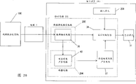
Fig. 1 is the block diagram that illustrates according to the example test equipment and the example display unit of the embodiment of the invention 1;
Fig. 2 is the exemplary plot of normal mode that illustrates the display unit of Fig. 1;
Fig. 3 is the exemplary plot that the test pattern that illustrates the testing equipment of Fig. 1 produces circuit;
Fig. 4 is the exemplary plot of data transmit circuit that illustrates the testing equipment of Fig. 1;
Fig. 5 is another exemplary plot of data transmit circuit that illustrates the testing equipment of Fig. 1;
Fig. 6 is the exemplary plot of phase modulation circuit that illustrates the testing equipment of Fig. 1;
Fig. 7 illustrates the data receiver circuit of display unit of Fig. 1 and the exemplary plot that control information produces circuit;
Fig. 8 illustrates the data receiver circuit of display unit of Fig. 1 and another exemplary plot that control information produces circuit;
Fig. 9 is the flow chart that illustrates according to the whole test process of the embodiment of the invention 1;
Figure 10 is the exemplary plot that illustrates according to the initialization flow process of the step 1 of Fig. 9 of the embodiment of the invention 1;
Figure 11 is the exemplary plot that illustrates according to the inspection flow process of the step 2 of Fig. 9 of the embodiment of the invention 1;
Figure 12 is the exemplary plot that illustrates according to the flow for displaying of the step 3 of Fig. 9 of the embodiment of the invention 1;
Figure 13 (a) is the exemplary plot of expression that illustrates the test video data of the check result view data that superposeed;
Figure 13 (b) is the exemplary plot that illustrates the expression of test video data;
Figure 14 is the exemplary plot that illustrates the check result image;
Figure 15 (a) is the exemplary plot that illustrates the expression of the check result view data that superposeed;
Figure 15 (b) is the exemplary plot that illustrates the expression of test video data;
Figure 16 is the block diagram that illustrates according to the example test equipment and the example display unit of the embodiment of the invention 2;
Figure 17 is the exemplary plot that illustrates according to the initialization flow process of the step 1 of Fig. 9 of the embodiment of the invention 2;
Figure 18 is the exemplary plot that illustrates according to the inspection flow process of the step 2 of Fig. 9 of the embodiment of the invention 2;
Figure 19 is the exemplary plot that illustrates according to the flow for displaying of the step 3 of Fig. 9 of the embodiment of the invention 2;
Figure 20 illustrates according to the example video data transmitter of the embodiment of the invention 3 and the block diagram of example display unit;
Figure 21 is the flow chart that illustrates according to the display unit under the test pattern of the embodiment of the invention 3;
Figure 22 (a) is the exemplary plot that illustrates the test signal that is received by data receiver circuit under test pattern;
Figure 22 (b) is the exemplary plot that illustrates the check result view data that is produced by check result image generation circuit under test pattern;
Figure 22 (c) is the exemplary plot that illustrates the view data that is shown by display unit under test pattern; With
Figure 23 is the block diagram that illustrates prior art digital of digital video data transmission/receiving system.
Embodiment
Now, will the present invention be described in greater detail with reference to the attached drawings according to embodiment.
[embodiment 1]
Fig. 1 is the block diagram that illustrates according to the example test equipment and the example display unit of the embodiment of the invention 1.
As shown in Figure 1, testing equipment 1 links to each other with display unit 3 by cable 5.
Test signal produces circuit 10 and comprises that test pattern produces circuit 15, clock signal generating circuit 16 and dither signal and produces circuit 17.
Test signal transtation mission circuit 11 comprises data transmit circuit 18 and phase modulation circuit 19.
Receiving circuit 30 comprises Data Receiving interlock circuit 34, check circuit 35, control signal receiving circuit 32, control signal transtation mission circuit 33, shows that commutation circuit 36 and check result image produce circuit 37.
Data Receiving interlock circuit 34 comprises data receiver circuit 38 and PLL (phase-locked loop) circuit 39.
Check circuit 35 comprises that control information produces circuit 40 and fault message produces circuit 41.
According to this configuration, the testing equipment 1 of Fig. 1 transmits test signal so that display unit 3 is carried out test by cable 5.Display unit 3 setup tests or the state of just carrying out test are called " test pattern ".
Typically, display unit 3 is launched the machine receiving video data to show at display unit 31 from video data.The normal condition of operation is called " normal mode ".
The configuration of the video data emission machine that will use in normal mode is described now, hereinafter.
Fig. 2 is the block diagram that illustrates the example video data transmitter that uses in normal mode.In Fig. 2, with identical Reference numeral represent with Fig. 1 in identical member.
As shown in Figure 2, video data emission machine 6 comprises that video produces circuit 60, clock signal generating circuit 61, data transmit circuit 62, control signal transtation mission circuit 63 and control signal receiving circuit 64.
For example, the video data emission machine such as video data emission machine 6 comprises personal computer or set-top box (STB).
Get back to Fig. 1, the test signal that describes below in the testing equipment 1 of Fig. 1 produces circuit 10.Test signal produces circuit 10 and produces test signal and it is outputed to test signal transtation mission circuit 11.
Specifically, the test signal that will describe in detail below as configuration as described in reference to figure 1 produces circuit 10.
The test pattern generation circuit 15 of testing equipment 1 at first, is described.
Fig. 3 is the exemplary plot that illustrates the test pattern generation circuit 15 of Fig. 1.As shown in Figure 3, test pattern generation circuit 15 comprises PN (pseudo noise) pattern generating circuit 150, test video data generating circuit 153 and commutation circuit 154.
PN pattern generating circuit 150 comprises shift register 151 and XOR circuit (EXOR circuit) 152.
PN pattern generating circuit 150 produces the PN pattern as test signal.According to the DVI standard, the generator polynomial that PN pattern generating circuit 150 uses is ((23 powers of x)+(5 powers of x)+1).The PN pattern is the example of test pattern.
Test video data generating circuit 153 produces the test video data as test signal.
Commutation circuit 154 bases are exported one of PN pattern or test video data from the switching signal of the control circuit 12 of Fig. 1.
The clock signal generating circuit 16 of the testing equipment 1 of Fig. 1 is described now, hereinafter.Clock signal generating circuit 16 clocking clk1 also output to phase modulation circuit 19 with it.
The dither signal generation circuit 17 of the testing equipment 1 of Fig. 1 is described now, hereinafter.Dither signal produces circuit 17 and produces dither signal clk2 and it is outputed to phase modulation circuit 19.
The test signal transtation mission circuit 11 of the testing equipment 1 of Fig. 1 is described now, hereinafter.
Test signal transtation mission circuit 11 is sent to display unit 3 with the test signal that test signal produces circuit 10 outputs by cable 5.
More specifically, will describe test signal transtation mission circuit 11 below in detail as configuration as described in reference to figure 1.
The data transmit circuit 18 of the testing equipment 1 of Fig. 1 at first, is described below.
Fig. 4 is the exemplary plot that illustrates the data transmit circuit 18 of Fig. 1.As shown in Figure 4, data transmit circuit 18 comprises 8B10B encoder circuit 180 and transmit amplifier 181.
8B10B encoder circuit 180 codings produce 8 Bit datas (PN pattern or test video data) of circuit 15 outputs by the test pattern of Fig. 1, comprise the 10 bit redundant codes (being called the 8B10B sign indicating number later on) of two redundant bits with generation.In the DVI standard, provided encryption algorithm used herein.
Transmit amplifier 181 amplifies the 8B10B sign indicating number that 8B10B encoder circuit 180 produces, and the coding that will obtain sends to the data receiver circuit 38 of the display unit 3 of Fig. 1 by the cable 5 of Fig. 1 then.
Fig. 5 is another exemplary plot of data transmit circuit 18 that illustrates the testing equipment 1 of Fig. 1.As shown in Figure 5, data transmit circuit 18 comprises transmit amplifier 181.
Transmit amplifier 181 amplifies the data (PN pattern or test video data) that produced circuit 15 outputs by the test pattern of Fig. 1, and the coding that will obtain sends to the data receiver circuit 38 of the display unit 3 of Fig. 1 by the cable 5 of Fig. 1 then.
In the time needn't following the DVI standard, can adopt circuit shown in Figure 5 as data transmit circuit 18.
The phase modulation circuit 19 of the testing equipment 1 of Fig. 1 is described now, hereinafter.
Fig. 6 is the exemplary plot that illustrates phase modulation circuit 19.As shown in Figure 6, phase modulation circuit 19 receives clock signal clk1 that is exported by the clock signal generating circuit 16 of Fig. 1 and the dither signal clk2 that is produced circuit 17 outputs by the dither signal of Fig. 1.
Then, phase modulation circuit 19 test pattern that output signal clk3 outputed to the testing equipment 1 of Fig. 1 as test signal produces circuit 15 and it is sent to the PLL circuit 39 of the display unit 3 of Fig. 1 by cable 5.
In this case, if the dither signal clk2 that is imported is not equal to " 0 ", then output signal clk3 is the clock signal that comprises shake.
On the other hand, if the dither signal clk2 that is imported equals " 0 ", if or dither signal clk2 " Aj " and " fj " equal " 0 ", then output signal clk3 is the clock signal that does not comprise shake.
The clock signal clk3 that comprises shake of the PN pattern generating circuit 150 of above-mentioned Fig. 3 and phase modulation circuit 19 outputs synchronously outputs to the PN pattern in the data transmit circuit 18 of testing equipment 1 of Fig. 1.
On the other hand, the clock signal clk3 that does not comprise shake of the test video data generating circuit 153 of Fig. 3 and phase modulation circuit 19 outputs synchronously outputs to the test video data in the data transmit circuit 18 of testing equipment 1 of Fig. 1.
The control circuit 12 of testing equipment 1 is described now, hereinafter.
Each circuit of control circuit 12 control testing equipments 1.This general gives suitable description with the explanation of whole testing process below.
The control signal transtation mission circuit 13 and the control signal receiving circuit 14 of the testing equipment 1 of Fig. 1 are described now, hereinafter.
Control signal transtation mission circuit 13 receives order to send the control signal receiving circuit 32 of test associated control signal to display unit 3 by cable 5 from control circuit 12.This general gives suitable description with the explanation of whole testing process below.
Control signal receiving circuit 14 is by the test associated control signal of cable 5 receptions by control signal transtation mission circuit 33 transmissions of display unit 3.This general gives suitable description with the explanation of whole testing process below.
The receiving circuit 30 of the display unit 3 of Fig. 1 is described now, hereinafter.
Receiving circuit 30 receives by the video data of Fig. 2 with normal mode launches the video data that machine 6 sends, and then it is outputed to the display unit 31 of display unit 3.On the other hand, receiving circuit 30 is with the test signal of test pattern reception by testing equipment 1 transmission of Fig. 1.
More specifically, the receiving circuit 30 of detailed descriptionwith reference 1 described configuration below.
The Data Receiving interlock circuit 34 of the display unit 3 of Fig. 1 at first, is described below.Data Receiving interlock circuit 34 receives the test signal by test signal transtation mission circuit 11 transmissions of the testing equipment 1 of Fig. 1 under test pattern.
On the other hand, Data Receiving interlock circuit 34 receives the video data by video data emission machine 6 transmissions of Fig. 2 under normal mode.
The check circuit 35 of the display unit 3 of Fig. 1 is described now, hereinafter.Check circuit 35 is checked Data Receiving interlock circuit 34 under test pattern, and produces inspection message it is outputed to check result image generation circuit 37.
The check result image generation circuit 37 of the display unit 3 of Fig. 1 is described now, hereinafter.The check result image produces circuit 37 and receive the inspection message that is produced by check circuit 35 under test pattern.
Then, the check result image produces the view data that circuit 37 produces the inspection message of expression input.
The view data of expression inspection message can be called " check result view data " hereinafter.On the other hand, the image of expression inspection message can be called " check result image " hereinafter.
The demonstration commutation circuit 36 of the display unit 3 of Fig. 1 is described now, hereinafter.Show that commutation circuit 36 outputs to display unit 31 with the video data that data receiver circuit 38 receives under normal mode.
On the other hand, in test pattern, show that commutation circuit 36 produces check result view data that circuit 37 produces with the check result image and is added on the test signal (PN pattern) that is received by data receiver circuit 38, so that resulting signal is outputed to display unit 31.
In addition, in test pattern, show that commutation circuit 36 produces check result view data that circuit 37 produces with the check result image and is added on the test signal (test video data) that is received by data receiver circuit 38, so that resulting signal is outputed to display unit 31.
Show that commutation circuit 36 provides the different operating between normal mode (not having stack) and the test pattern (stack is arranged).Control signal receiving circuit 32 receives control signal from testing equipment 1, will show that then switching signal outputs to demonstration commutation circuit 36 to carry out the switching between these operations.
The control signal receiving circuit 32 and the control signal transtation mission circuit 33 of the display unit 3 of Fig. 1 are described now, hereinafter.
Control signal receiving circuit 32 passes through the test associated control signal of cable 5 receptions by control signal transtation mission circuit 13 transmissions of testing equipment 1 under test pattern.This general gives suitable description with the explanation of whole testing process below.
On the other hand, utilization is used for the member 8 of acceptance test associated control signal (for example when receiving circuit 30 is configured to integrated circuit, the pin that is used for the acceptance test associated control signal), control signal receiving circuit 32 receives under normal mode by the video data of Fig. 2 and launches the control signal of the control signal transtation mission circuit 63 of machine 6 by cable 5 transmissions.
Control signal transtation mission circuit 33 will be tested associated control signal sends to testing equipment 1 by cable 5 control signal receiving circuit 14 under test pattern.This general gives suitable description with the explanation of whole testing process below.
On the other hand, utilization is used to send the member 9 of test associated control signal (for example when receiving circuit 30 is configured to integrated circuit, be used to send the pin of test associated control signal), control signal transtation mission circuit 33 sends to control signal the control signal receiving circuit 64 of the video data emission machine 6 of Fig. 2 by cable 5 under normal mode.
Now, be described in more detail below Data Receiving interlock circuit 34.Data Receiving interlock circuit 34 with reference to figure 1 described configuration is described below.
The PLL circuit 39 of Fig. 1 at first, is described below.PLL circuit 39 produces under test pattern and the synchronous timing signal of clock signal clk3 that is passed through cable 5 transmissions by the phase modulation circuit 19 of testing equipment 1.
Then, timing signal is outputed to data receiver circuit 38 and fault message and produce circuit 41.
On the other hand, in normal mode, PLL circuit 39 produces and is launched the clock signal synchronous timing signal of the clock signal generating circuit 61 of machine 6 by cable 5 transmissions by the video data of Fig. 2, then timing signal is outputed to data receiver circuit 38.
The data receiver circuit 38 of Fig. 1 is described now, hereinafter.The timing signal that data receiver circuit 38 is exported with PLL circuit 39 under test pattern is synchronously caught the test signal by data transmit circuit 18 transmissions of testing equipment 1.
Then, the test signal of being caught is outputed to demonstration commutation circuit 36 and control information and produce circuit 40.
On the other hand, in normal mode, data receiver circuit 38 is synchronously caught the video data of being launched data transmit circuit 62 transmissions of machine 6 by the video data of Fig. 2 with the timing signal of PLL circuit 39 outputs, video data is outputed to show commutation circuit 36 then.
Now, be described in more detail below the check circuit 35 of Fig. 1.Check circuit 35 with reference to figure 1 described configuration is described below.
At first, control information is described below and produces circuit 40.In test pattern, control information produces the data error information that circuit 40 produces the test signal (PN pattern) that receives about data receiver circuit 38, then, resulting signal is outputed to the check result image produce circuit 37 as inspection message.
As example, the situation of generation " data error rate (bit error rate (BER)) " as data error information is described below.
Fig. 7 illustrates the data receiver circuit 38 of display unit 3 of Fig. 1 and the exemplary plot that control information produces circuit 40.
As shown in Figure 7, data receiver circuit 38 comprises reception amplifier 380 and 8B10B decoder circuit 381.
Control information produces circuit 40 and comprises PN pattern generating circuit 400, data comparator circuit 401, counter 402 and divider circuit 403.
In test pattern, 8 Bit datas that also will decode output to the data comparator circuit 401 of Fig. 7.In test pattern, because testing equipment 1 sends the PN pattern that is produced by PN pattern generating circuit 150 (Fig. 3), 8 Bit datas of decoding are the PN patterns.
The PN pattern generating circuit 400 of Fig. 7 produces the identical PN pattern that is produced with the PN pattern generating circuit 150 (Fig. 3) of testing equipment 1.
402 pairs of inconsistent signal-count of counter will represent that then the information of count number is sent to divider circuit 403.
In this case, the number of inspection bit is a bit number of checking each circulation of flow process.In the explanation of the whole testing process of describing after a while, this will be clearer.
To represent that the information of the data error rate of judgement outputs to the check result image generation circuit 37 of Fig. 1 as inspection message by this way.
Fig. 8 illustrates the data receiver circuit 38 of display unit 3 of Fig. 1 and another exemplary plot that control information produces circuit 40.In Fig. 8, with identical Reference numeral represent with Fig. 7 in identical member.
As shown in Figure 8, data receiver circuit 38 comprises reception amplifier 380.
Control information produces circuit 40 and comprises PN pattern generating circuit 400, data comparator circuit 401, counter 402 and divider circuit 403.
In test pattern, also the data of amplifying are outputed to the data comparator circuit 401 of Fig. 8.In test pattern, because testing equipment 1 sends the PN pattern that PN pattern generating circuit 150 (Fig. 3) produce, so the data of amplifying are the PN patterns.
It is identical with the control information generation circuit 40 of Fig. 7 that the control information of Fig. 8 produces circuit 40.
The fault message generation circuit 41 of Fig. 1 is described now, hereinafter.In test pattern, fault message produces circuit 41 and receives the timing signal that is produced by PLL circuit 39 according to the clock signal clk3 that comprises shake, produce the fault message of PLL circuit 39 then, produce circuit 37 as inspection message the signal that obtains is given the check result image.
As example, describe the situation of the losing lock signal of generation PLL circuit below in detail as fault message.
The loss of lock (losing lock) of PLL circuit is described below in normal way.The PLL circuit produces and the synchronous output clock (timing signal) of input clock.Loss of lock (losing lock) means that the PLL circuit can not produce the output clock (timing signal) synchronous with input clock, and phase place keeps unsure state.
On the other hand, the state that the PLL circuit produces with the synchronous output clock (timing signal) of input clock is called as PLL circuit " locking ", otherwise the PLL circuit is lost the state of locking and is called as " loss of lock (losing lock) ".
Now, in an embodiment, PLL circuit 39 can not produce the synchronous timing signal of the clock signal clk3 that comprises shake that the phase modulation circuit 19 with testing equipment 1 receives, thereby makes the timing signal phase-unstable.In this case, fault message produces circuit 41 output losing lock signals and produces circuit 37 as inspection message to the check result image.
The device of the loss of lock (losing lock) that is used to detect the PLL circuit for example, is disclosed in the uncensored patent disclosure of Japan Hei-7-170179 number.In this embodiment, might adopt this device to produce circuit 41 as fault message.
The check result image produces circuit 37 and exists or non-existent information according to the losing lock that fault message produces the losing lock signal generation expression PLL circuit 39 of circuit 41 outputs.
Then, the check result image produces circuit 37 and produces expression data error rate and losing lock existence or non-existent view data (check result view data).
The above-mentioned receiving circuit 30 of Fig. 1 can be configured to integrated circuit (LSI).
Can use term " member " below.For the receiving circuit 30 that is configured to LSI, " member " means " pin " that is used for input/output signal among the LSI.Certainly, even receiving circuit 30 is being configured under the situation of LSI, " member " also can comprise other known terminal.
The display unit 31 of the display unit 3 of Fig. 1 is described now, hereinafter.Display unit 31 shows the video data of commutation circuit 36 outputs with normal mode.
On the other hand, in test pattern, display unit 31 show by show commutation circuit 36 outputs, by go up the view data that the check result view data that superposes produces in test signal (PN pattern or test video data).
Now, hereinafter with reference to figure 1 and flow chart description whole testing process according to embodiment.
Fig. 9 is the flow chart that is used for testing equipment 1 and display unit 3 according to this embodiment.
As shown in Figure 9, at first, in step 1, initialization test equipment 1.Then, in step 2, check display unit 3.Then, in step 3, on the display unit 31 of display unit 3, show the check result view data.
Now, be described in more detail below processing in each step of Fig. 9.
Figure 10 illustrates the initialization flow process of the step 1 of Fig. 9.With reference to Figure 10, the processing on the left side shows the processing of testing equipment 1, and the processing of display unit 3 is represented in the processing on the right.
As shown in figure 10, at first, in step 10, initialization test equipment 1.More specifically, following description step.
Then, in step 11, testing equipment 1 indicated number device 3 begins test.More specifically, can description step as follows.
The control unit 12 command-control signal transtation mission circuits 13 of testing equipment 1 will order the control signal of test beginning to be sent to the control signal receiving circuit 32 of display unit 3.
In response to this, the control signal transtation mission circuit 13 of testing equipment 1 will order the control signal of test beginning to be sent to the control signal receiving circuit 32 of display unit 3.
In response to this, in step 12, the control signal receiving circuit 32 of display unit 3 will show that switching signal outputs to demonstration commutation circuit 36 and shows commutation circuit 36 to connect.
In response to this, in step 13, the control signal that the control signal transtation mission circuit 33 of display unit 3 will notify test to be ready to complete sends to the control signal receiving circuit 14 of testing equipment 1.
This makes display unit 3 be in test pattern.
In response to this, in step 14, the control signal receiving circuit 14 of testing equipment 1 receives to be used to notify tests the control signal that is ready to complete, then with its notice control circuit 12.
Then, handle the step 2 that proceeds to Fig. 9.
Figure 11 illustrates the inspection flow process of the step 2 of Fig. 9.With reference to Figure 11, the processing on the left side shows the processing of testing equipment 1, and the processing of display unit 3 is represented in the processing on the right.
As shown in figure 11, at first, in step 20, the clock signal clk3 that the phase modulation circuit 19 of testing equipment 1 will comprise shake outputs to the PLL circuit 39 that test pattern produces circuit 15 and display unit 3.
In response to this, in step 21, the test pattern of testing equipment 1 produce the clock signal that comprises shake that circuit 15 outputs and phase modulation circuit 19 provide synchronous have a constant number of bits purpose PN pattern.
Then, the data transmit circuit 18 of testing equipment 1 sends to the PN pattern data receiver circuit 38 of display unit 3.
On the other hand, in step 22, the PLL circuit 39 of display unit 3 produces and the synchronous timing signal of the clock signal clk3 that is received that comprises shake.Subsequently, PLL circuit 39 outputs to data receiver circuit 38 and fault message generation circuit 41 with the timing signal that produces.
In response to this, in step 23, when PLL circuit 39 was in out-of-lock condition, the fault message of having imported timing signal produced circuit 41 and produces the losing lock signal, then it is outputed to the check result image and produces circuit 37 as inspection message.
On the other hand, in step 24, the timing signal that the data receiver circuit 38 and the PLL circuit 39 of display unit 3 provides is synchronously caught the PN pattern by data transmit circuit 18 transmissions of testing equipment 1.
Then, data receiver circuit 38 outputs to demonstration commutation circuit 36 and control information generation circuit 40 with the PN pattern that receives as receiving data.
In response to this, in step 25, control information produces the data error rate of circuit 40 determinating receiving datas, then the signal that obtains is outputed to the check result image as inspection message and produces circuit 37.
Then, in step 26, the check result image of display unit 3 produces circuit 37 delegation's inspection message (losing lock of chattering frequency, PLL circuit 39 exists or do not exist and the data error rate) is produced the view data (check result view data) of expression inspection message mutually, shows commutation circuit 36 thereby output to.
Inspection message (losing lock of chattering frequency, PLL circuit 39 exists or do not exist and the data error rate) is stored in the memory circuit (not shown).
Then,, show that commutation circuit 36 goes up stack in the reception data (PN pattern) by data receiver circuit 38 outputs and produces the check result view data of circuit 37 outputs by the check result image, then the signal that obtains is outputed to display unit 31 in step 27.
Then, in step 28, display unit 31 shows the reception data (PN pattern) of check result view data that superposeed on it.
Then,, then handle the step 3 that proceeds to Fig. 9 if finished inspection, otherwise, handle proceeding to step 30 (step 29).
In step 30, the control circuit 12 of testing equipment 1 changes the chattering frequency that dither signal produces circuit 17.Then, this is handled with this processing of chattering frequency execution from step 20 to step 29.
The bit number of each circulation is a number of checking bit in the inspection flow process shown in Figure 11.The control information of Fig. 7 and Fig. 8 produce circuit 40 with inconsistent bit number in the PN pattern divided by checking bit number, thereby specified data error rate (bit error rate (BER)).
Now, be described in more detail below the processing of the step 3 of Fig. 9.
Figure 12 illustrates the flow for displaying of the step 3 of Fig. 9.With reference to Figure 12, the processing on the left side shows the processing of testing equipment 1, and the processing of display unit 3 is represented in the processing on the right.
As shown in figure 12, at first, in step 31, the generation that the control circuit 12 order dither signals of testing equipment 1 produce circuit 17 deactivations (deactivate) dither signal.
In response to this, dither signal produces circuit 17 and gets 0 by jitter amplitude Aj and chattering frequency fj with dither signal clk2, comes the generation of deactivation dither signal clk2.
In response to this, in step 32, the clock signal clk3 that the phase modulation circuit 19 of testing equipment 1 will not comprise shake outputs to the PLL circuit 39 that test pattern produces circuit 15 and display unit 3.
In step 33, the control circuit 12 of testing equipment 1 outputs to the commutation circuit 154 (Fig. 3) that test pattern produces circuit 15 with switching signal, thereby switch test pattern generating circuit 15 is with output test video data.
In response to this, in step 34, test pattern produces circuit 15 and synchronously exports the test video data with the clock signal that does not comprise shake of phase modulation circuit 19 outputs.
Then, the data transmit circuit 18 of testing equipment 1 sends to the test video data data receiver circuit 38 of display unit 3.
On the other hand, in step 35, PLL circuit 39 generations of display unit 3 and the synchronous timing signal of the clock signal that does not comprise shake of phase modulation circuit 19 transmissions of testing equipment 1.
Then, PLL circuit 39 outputs to data receiver circuit 38 with the timing signal that produces.
In response to this, in step 36, the timing signal of the data receiver circuit 38 of display unit 3 and 39 outputs of PLL circuit is synchronously caught the test video data by data transmit circuit 18 transmissions of testing equipment 1.
Then, data receiver circuit 38 outputs to demonstration commutation circuit 36 with the test video data that receive as receiving data.
On the other hand, in step 37, the check result image of display unit 3 produces circuit 37 and obtain inspection message (losing lock of chattering frequency, PLL circuit 39 exists or do not exist and the data error rate) from the memory circuit (not shown), to produce the view data (check result view data) of expression inspection message.
Then, the check result image produces circuit 37 the check result view data that produces is outputed to demonstration commutation circuit 36.
Then, in step 38, the check result view data that the demonstration commutation circuit 36 of display unit 3 produces circuit 37 outputs with the check result image is added on the reception data (test video data) of data receiver circuit 38 outputs, and the signal that obtains is outputed to display unit 31.
In response to this, in step 39, the display unit 31 of display unit 3 shows the test video data of check result view data that superposeed on it.
Now, provide the example of demonstration hereinafter.
Figure 13 shows the exemplary view of the view data that will show on the display unit 31 of display unit 3 in the step 39 of Figure 12.
Figure 13 (a) is the example when the demonstration that is provided when opening from the demonstration switching signal of the control signal receiving circuit 32 of Fig. 1, and Figure 13 (b) is the example when the demonstration that provides for Guan Shisuo from the demonstration switching signal of the control signal receiving circuit 32 of Fig. 1.
In the step 12 of Figure 10, control signal receiving circuit 32 makes the demonstration switching signal can connect demonstration commutation circuit 36.
Shown in Figure 13 (a), this makes the test video data of stack check result view data be presented on the display unit 31 of display unit 3.
More specifically, test pattern A is presented on the main screen 310 of display unit 31, and the check result image B is presented on the secondary screen 311.
On the other hand, suppose that the control signal receiving circuit 32 of display unit 3 has received the control signal of control signal transtation mission circuit 13 transmissions of testing equipment 1, and closed switching signal by order.In this case, demonstration commutation circuit 36 is closed, thereby makes the test video data export on display unit 31.
In this case, shown in Figure 13 (b), have only test pattern A to be presented on the main screen 310 of display unit 31.
Figure 14 is the exemplary plot that illustrates the check result image B that will show on the secondary screen 311 of the display unit 31 of Figure 13.
As shown in figure 14, the losing lock of chattering frequency, PLL circuit 39 exists or does not exist and the data error rate shows as the check result image on the secondary screen 311 of display unit 31.In the losing lock existence or non-existent expression of PLL circuit, the lock-out state of " OK " expression PLL circuit, and the out-of-lock condition of " NG " expression PLL circuit.
Now, the replacement method that shows has been described hereinafter.
The demonstration commutation circuit 36 of the testing equipment 1 of Fig. 1 is superimposed upon the check result view data on the test video data, and the signal that obtains is outputed to display unit 31.Yet, can adopt to show that commutation circuit 36 is as the simple commutation circuit of not having this class stack.
That is to say, suppose step 12, connect demonstration commutation circuit 36 thereby control signal receiving circuit 32 has activated the demonstration switching signal at Figure 10.In this case, show that commutation circuit 36 will be outputed on the display unit 31 by the check result view data that the check result image produces circuit 37 outputs, and do not carry out the stack in the step 38 of Figure 12.
On the other hand, suppose that the control signal receiving circuit 32 of display unit 3 has received the control signal of control signal receiving circuit 14 transmissions of testing equipment 1, and be instructed to close the demonstration switching signal.In this case, demonstration commutation circuit 36 is closed, and makes the test video data are outputed on the display unit 31.
Below with reference to accompanying drawing these main points have been described.
Figure 15 shows another exemplary plot of the view data that shows on the step 39 of Figure 12 will the display unit 31 in display unit 3.
Figure 15 (a) is the example shown that is provided when opening when from the demonstration switching signal of the control signal receiving circuit 32 of Fig. 1, and Figure 15 (b) is the example shown that provides for Guan Shisuo when the demonstration switching signal from the control signal receiving circuit 32 of Fig. 1.
Shown in Figure 15 (a), in the step 39 of Figure 12, for simple the employing shows commutation circuit 36 as commutation circuit, the check result image B is presented on the main screen 310 of display unit 31.For example, the check result image B that shows here is an image shown in Figure 14.
On the other hand, suppose to show that switching signal shows that for the pass commutation circuit 36 is also for closing.In this case, shown in Figure 15 (b), test pattern A is presented on the main screen 310 of display unit 31.
In an embodiment, timing signal and the clock signal that comprises shake synchronously are provided to the data receiver circuit 38 (seeing the step 20 and 22 of Figure 11) of the display unit 3 of Fig. 1.This feasible influence that may learn shake by the measurement data error rate.Other principal element that influences the data error rate comprises the noise from other circuit, and therefore the data error rate comprises the influence that noise causes.
In addition, in this embodiment, will comprise that the clock signal of shake is provided to the PLL circuit 39 of the display unit 3 of Fig. 1 (seeing the step 20 and 22 of Figure 11).This makes and may learn the influence of shake to PLL circuit 39 by detecting the losing lock signal.Other principal element that influences PLL circuit 39 comprises the noise from other circuit, and therefore the losing lock of PLL circuit 39 comprises the influence that noise causes.
The operation of test pattern has been described.Now, with reference to figure 2, the operation of normal mode is described briefly hereinafter.
As shown in Figure 2, the control signal transtation mission circuit 63 of video data emission machine 6 control signal that will be used to notify video data to send sends to the control signal receiving circuit 32 of display unit 3 by cable 5.
In response to this, be used for the member 8 (for example comprising the pin that is provided under the situation of integrated circuit) of acceptance test associated control signal at receiving circuit 30, control signal receiving circuit 32 receives control signal.
In response to this, utilization is used to send the member 9 (for example comprising the pin that is provided under the situation of integrated circuit at receiving circuit 30) of test associated control signal, and the control signal transtation mission circuit 33 of display unit 3 will send to the control signal receiving circuit 64 of video data emission machine 6 such as the display control information of the resolution of display unit 3 by cable 5.
Clock signal generating circuit 61 clockings of video data emission machine 6 are to send it to the PLL circuit 39 of video generation circuit 60 and display unit 3.
The clock signal that video generation circuit 60 and clock signal generating circuit 61 provide is the output video data synchronously.
Then, data transmit circuit 62 video data that video is produced circuit 60 output sends to the data receiver circuit 38 of display unit 3 by cable 5.
The data receiver circuit 38 of display unit 3 is caught and the timing signal synchronized video data, and timing signal is produced by PLL circuit 39 and be synchronous with clock signal.
At this moment, owing to show that commutation circuit 36 is an off status, so video data is output to display unit 31 for demonstration.
As mentioned above, following content is suitable for the display unit 3 according to present embodiment.
That is to say, in this embodiment, provide check circuit 35 in display unit 3 inside of Fig. 1.Therefore,, check Data Receiving interlock circuit 34, and produce inspection message (data error rate and losing lock signal) in display unit 3 inside.
Then, the check result image produces the view data (check result view data) that circuit 37 produces the expression inspection messages, and the check result view data is presented on the display unit 31 that display unit 3 provides (Figure 13 is to Figure 15).
As a result, may carry out in assembling display unit 3 backs and check, and need not to dismantle display unit 3.Thereby this feasible might execution the Data Receiving interlock circuit 34 of display unit 3 inside with plain mode is tested, and does not change the noisy environment of display unit 3 inside.
In addition, owing on the display unit 31 of incorporating display unit 3 inside into, show the check result view data, so need outside display unit 3, not provide attaching terminal with outgoing inspection result images data.
And the control signal receiving circuit 32 of display unit 3 is from testing equipment 1 acceptance test associated control signal.In addition, control signal receiving circuit 32 can receive and handle the external signal except that the test associated control signal by the member 8 that is used for the acceptance test associated control signal.
Subsequently, received from testing equipment 1 at control signal receiving circuit 32 be used to indicate the test beginning control signal as after the test associated control signal, display unit 3 enters test pattern.
As mentioned above, the control signal receiving circuit 32 of display unit 3 can receive and handle the external signal except that the test associated control signal.This makes display unit 3 to change to normal mode by indicating its external control signal that turns back to normal mode to send to control signal receiving circuit 32.In addition, display unit 3 can send to control signal receiving circuit 32 from its outside testing equipment 1 by the control signal that only will indicate the test beginning, enters test pattern.
That is to say, can only come switch mode by the control signal of display unit 3 outsides.
As a result, this makes and might carry out test to the Data Receiving interlock circuit 34 of display unit 3 inside with plain mode.
In addition, because the control signal receiving circuit 32 of display unit 3 can receive and handle the external signal except that the test associated control signal, so control signal receiving circuit 32 can receive and handle the signal that is sent by its outside video data emission machine 6.
This makes that external video data transmitter 6 may be after entering normal mode, and the signal of needs is sent to control signal receiving circuit 32.
As mentioned above, the invention provides the control signal receiving circuit 32 that under test pattern, can under normal mode, work again.
And when receiving external signal, control signal receiving circuit 32 can use standard member 8 under test pattern or normal mode.
This has eliminated the demand of the additional member of acceptance test associated control signal only, thereby makes and might avoid increasing and the compatible shortcoming of losing (with the pin compatibility loss of other LSI) of member such as package area.
On the other hand, the control signal transtation mission circuit 33 of display unit 3 can send the test associated control signal.In addition, control signal transtation mission circuit 33 can be by being used for that the test associated control signal is sent to the signal that outside member 9 sends except that testing associated control signal.
This makes control signal transtation mission circuit 33 to send signal to external video data transmitter 6 by being used for that the test associated control signal is sent to outside member 9.
This makes that control signal transtation mission circuit 33 may be after entering normal mode, and the signal of needs is sent to external video data transmitter 6.
As mentioned above, the invention provides can again can be at the control signal transtation mission circuit 33 of normal mode work under test pattern.
And when when the outside sends signal, control signal transtation mission circuit 33 can use standard member 9 under test pattern or normal mode.
This has eliminated to display unit 3 provides the demand that only is used to send the additional member of testing associated control signal, thereby makes the shortcoming that might avoid for example package area increase and the compatible loss of member (with the pin compatibility loss of other LSI).
On the other hand, in test pattern, the demonstration commutation circuit 36 of display unit 3 is superimposed upon the check result view data that the check result image produces circuit 37 generations on the test signal of being imported by data receiver circuit 38 (test video data), then the signal that obtains is outputed to display unit 31.
This makes the check result of the Data Receiving interlock circuit 34 in the display unit 31 might check display unit 3.Also may send the test video data and the test video data be carried out visual inspection (seeing Figure 13 (a)) as test signal by the outside.
And, according to pattern, show that will superpose one of the video data of check result view data or test video data of commutation circuit 36 output to display unit 31.This makes might share the member and the member that is used for the test video data of the check result view data that superposeed are outputed to display unit 31 that is used for video data is outputed to display unit 31.
This eliminated provide only be used for from the stack that shows commutation circuit 36 the test video data of check result view data output to the demand of the additional member of display unit 31.This makes might avoid for example package area increase and the compatible shortcoming of losing (with the pin compatibility loss of other LSI) of member.
On the other hand, when adopting demonstration commutation circuit 36 simply, show commutation circuit 36, and it is outputed to display unit 31 under normal mode from data receiver circuit 38 receiving video datas as commutation circuit.Under test pattern, show that commutation circuit 36 receives the check result view data that is produced circuit 37 generations by the check result image, outputs to it display unit 31 then.
This makes the check result of the Data Receiving interlock circuit 34 in the display unit 31 might check display unit 3.(seeing Figure 15 (a))
In addition, when showing commutation circuit 36 simply, can eliminate the function that enables to superpose, show commutation circuit 36 thereby may simplify as commutation circuit.
And according to pattern, the demonstration commutation circuit 36 that is used simply as commutation circuit produces one of check result view data that circuit 37 produces with video data or check result image and outputs to display unit 31.This makes might share the member and the member that is used for the check result view data that check result image generation circuit 37 produces is outputed to display unit 31 that is used for video data is outputed to display unit 31.
Demand that only is used for the check result view data from the demonstration commutation circuit 36 that is used simply as commutation circuit is outputed to the additional member of display unit 31 that provides has been provided for this.This makes might avoid for example package area increase and the compatible shortcoming of losing (with the pin compatibility loss of other LSI) of member.
In addition, in test pattern, be used simply as the control signal of the demonstration commutation circuit 36 of commutation circuit according to the indicated number conversion of control signal receiving circuit 32 receptions, the receiving check result images produces the check result view data that circuit 37 produces, data are outputed to display unit 31.Replacedly, show commutation circuit 36 acceptance test video datas, export the test video data then to display unit 31 as test signal.
As mentioned above, under test pattern, the demonstration commutation circuit 36 that is used simply as commutation circuit outputs to display unit 31 according to control signal with one of check result view data or test video data.This makes might share the member and the member that is used for the test video data are outputed to display unit 31 that is used for the check result view data is outputed to display unit 31.
This has eliminated to provide and only has been used for and will outputs to the demand of the additional member of display unit 31 from the data under the test pattern of the demonstration commutation circuit 36 that is used simply as commutation circuit (check result view data and test video data).This makes might avoid for example package area increase and the compatible shortcoming of losing (with the pin compatibility loss of other LSI) of member.
Also may transmit control signal and the test video data of the display unit 31 of display unit 3 are carried out visual inspection (seeing Figure 13 (a) and 15 (b)) by the outside.
On the other hand, the data receiver circuit 38 of display unit 3 receiving video data under normal mode, and under test pattern, receive the PN pattern as test signal.
Then, in test pattern, the control information of display unit 3 produces the data error rate that circuit 40 produces the PN pattern that is received by data receiver circuit 38.The data error rate is presented on the display unit 31 and (sees Figure 14) then.
As a result, this makes might carry out inspection after assembling display unit 3, and need not to dismantle display unit 3.Test (measurement of data error rate) thereby this makes to carry out the data receiver circuit 38 of display unit 3 inside with plain mode, and do not change the noisy environment of display unit 3 inside.
On the other hand, PLL circuit 39 is the receive clock signal under normal mode, and the clock signal that reception simultaneously comprises shake is as test signal, and the generation timing signal synchronous with it.
Then, in test pattern, when PLL circuit 39 losing locks, fault message produces circuit 41 and produces the losing lock signal.On display unit 31, show the existence of losing lock or do not have (seeing Figure 14).
As a result, this makes might carry out inspection after assembling display unit 3, and need not to dismantle display unit 3.Test (detection of losing lock signal) thereby this makes to carry out the PLL circuit 39 of display unit 3 inside with plain mode, and do not change the noisy environment of display unit 3 inside.
Owing to checked PLL circuit 39 and data receiver circuit 38, decidable is by PLL circuit 39 or other sends the fault that degradation factors causes display unit 3.This feasible specifically reason of the fault of identification display device 3.
On the other hand, the data receiver circuit 38 of display unit 3 receives and the timing signal synchronized video data based on clock signal under normal mode, receives the PN pattern as test signal synchronous with timing signal based on the clock signal that comprises shake simultaneously.
Can judge the data error rate of the PN pattern that receives synchronously with timing signal by this way, thereby the conclusion (findings) of relevant effect of jitter is provided.
On the other hand, in an embodiment, check circuit 35 is checked Data Receiving interlock circuit 34 with the generation inspection message, and shows the view data (check result view data) of expression inspection message on display unit 31.
As a result, compare with situation about only estimating by the execution of people's eyesight, this makes might provide more accurate target check result.
As mentioned above, following content is applicable to for the testing equipment 1 according to present embodiment.
That is to say that in an embodiment, the control signal transtation mission circuit 13 of testing equipment 1 receives order from control circuit 12, will indicate the control signal of test beginning to send to display unit 3 then.
By this way, the display unit 3 that is used for the acceptance test signal can be that test is got ready by the plain mode that only control signal is sent to display unit 3.
On the other hand, the control circuit 12 of testing equipment 1 is indicated to the dither signal generation circuit 17 that test signal produces circuit 10 with chattering frequency as test condition.
This has alleviated time and the manpower that is used to be provided with the chattering frequency that is provided with by hand traditionally.
The test pattern of testing equipment 1 produces circuit 15 and produces the PN pattern as test signal.Then the PN pattern is sent to display unit 3.
This feasible data error rate that might judge the PN pattern that receives by the data receiver circuit in the display unit 3 38.
In addition, the phase modulation circuit 19 of testing equipment 1 is superimposed upon dither signal clk2 on the clock signal clk1, comprises the clock signal clk3 of shake with generation, and the clock signal clk3 that will comprise shake then sends to the PLL circuit 39 of display unit 3 as test signal.
This makes and might learn the influence of shake to PLL circuit 39 in the display unit 3 by the losing lock signal that detects PLL circuit 39.
The test pattern of testing equipment 1 produces circuit 15 and synchronously the PN pattern is outputed to data transmit circuit 18 with the clock signal that comprises shake that phase modulation circuit 19 produces.
This makes might be in display unit 3, and the data error rate of the PN pattern that receives according to data receiver circuit 38 is learnt the influence of shake.
This makes might provide the conclusion of the influence of cable in the inspection to the Data Receiving interlock circuit 34 (data receiver circuit 38 and PLL circuit 39) of display unit 3.
The available testing equipment 1 that is not directly connected to display unit 3 by cable 5 is carried out test.
In addition, when need when the display unit 31 of display unit 3 is carried out the range estimation of test video data, not removing the test video data generating circuit 153 of Fig. 3.
In this case, use the demonstration commutation circuit 36 of display unit 3 of Fig. 1 as commutation circuit simply.
[embodiment 2]
In an embodiment, different with embodiment 1, testing equipment to produce the check result view data, then sends it to display unit from display unit receiving check information.To describe in detail below.
Figure 16 is the block diagram that illustrates according to the example test equipment 1 and the example display unit of the embodiment of the invention 2.With reference to Figure 16, be marked by identical Reference numeral with member identical among Fig. 1, and will the descriptions thereof are omitted when suitable.
As shown in figure 16, testing equipment 8 links to each other with display unit 7 by cable 5.
Testing equipment 8 comprises that test signal produces circuit 80, test signal transtation mission circuit 11, control circuit 12, control signal transtation mission circuit 13, control signal receiving circuit 14, check result image generation circuit 82 and inspection message memory circuit 83.
Test signal produces circuit 80 and comprises that test pattern produces circuit 15, clock signal generating circuit 16, dither signal generation circuit 17 and supercircuit 81.
Test signal transtation mission circuit 11 comprises data transmit circuit 18 and phase modulation circuit 19.
Display unit 7 comprises receiving circuit 70 and display unit 31.
Receiving circuit 70 comprises Data Receiving interlock circuit 34, check circuit 35, control signal receiving circuit 32 and control signal transtation mission circuit 33.
Data Receiving interlock circuit 34 comprises data receiver circuit 38 and PLL (phase-locked loop) circuit 39.
Check circuit 35 comprises that control information produces circuit 40 and fault message produces circuit 41.
Similar with the receiving circuit 30 of Fig. 1, receiving circuit 70 can be configured to integrated circuit (LSI).
Can use term " member " below.For the receiving circuit 70 that is configured to LSI, " member " means the signal I/O " pin " of LSI.Certainly, even be configured at receiving circuit 70 under the situation of LSI, " member " also can comprise other known terminal.
According to this configuration, the testing equipment 8 of Figure 16 transmits test signal so that display unit 7 is carried out test by cable 5.The state that display unit 7 has been ready to test or just carrying out test is called " test pattern ".
Typically, display unit 7 is launched machine 6 receiving video datas to be presented on the display unit 31 from the video data of Fig. 2.This normal condition of operation is called " normal mode ".Identical among the operation of normal mode and the embodiment 1.
Now, when comparing with the display unit 3 of Fig. 1, the display unit 7 of Figure 16 does not provide and shows that commutation circuit 36 and check result image produce circuit 37.The same with the display unit 3 of Fig. 1, the display unit 7 of Figure 16 also provides other member, and therefore the descriptions thereof are omitted.
Yet, in this configuration, will produce the information of the expression data error rate that circuit 40 produces and produce the losing lock signal that circuit 41 produces by control information and output to control signal transtation mission circuit 33 by fault message.
Testing equipment 8 has test pattern and produces circuit 15, clock signal generating circuit 16, dither signal and produce circuit 17, test signal transtation mission circuit 11, control circuit 12, control signal transtation mission circuit 13 and control signal receiving circuit 14, and it produces circuit 15, clock signal generating circuit 16, dither signal with the test pattern of the testing equipment 1 of Fig. 1 respectively, and to produce circuit 17, test signal transtation mission circuit 11, control circuit 12, control signal transtation mission circuit 13 identical with control signal receiving circuit 14.Therefore omit description to these members.
Yet, according to this configuration, the inspection message (there is or does not exist and represent the information of data error rate in the losing lock of PLL circuit 39) that the control signal transtation mission circuit 33 of control signal receiving circuit 14 receiving and displaying devices 7 sends outputs to information inspection message memory circuit 83 then.
Inspection message memory circuit 83 storage inspection messages.The check result image produces circuit 82 and obtains inspection message from inspection message memory circuit 83, to produce the view data of expression inspection message.
The view data of expression inspection message can be called " check result view data " below.On the other hand, the image of expression inspection message can be called " check result image " below.
The check result image produces circuit 82 the check result view data that produces is outputed to supercircuit 81.
Supercircuit 81 is superimposed upon test pattern with the check result view data and produces on the test signal (PN pattern or test video data) that circuit 15 produced, and then the signal that obtains is outputed to data transmit circuit 18.
Then, the data receiver circuit 38 of display unit 7 receives the test signal of the check result view data that superposeed from the data transmit circuit 18 of testing equipment 8, then the signal that obtains is outputed to display unit 31.Display unit 31 shows the test signal of the check result view data that superposeed.
Now, hereinafter with reference to Figure 16 and flow chart description whole testing process according to present embodiment.
Whole testing process according to present embodiment is identical with flow chart shown in Figure 9, and therefore makes following description with reference to figure 9.
As shown in Figure 9, at first, in step 1, initialization test equipment 8.Then, in step 2, check display unit 7.Then, in step 3, on the display unit 31 of display unit 7, show the check result view data.
Now, be described in more detail below processing in each step of Fig. 9.
Figure 17 illustrates the initialization flow process of the step 1 of Fig. 9.With reference to Figure 17, the processing on the left side shows the processing of testing equipment 8, and the processing of display unit 7 is represented in the processing on the right.
As shown in figure 17, at first, in step 10, initialization test equipment 8.More specifically, this step of following description.
The control circuit 12 of testing equipment 8 outputs to commutation circuit 154 (Fig. 3) that test pattern produces circuit 15 with switch test pattern generating circuit 15 with switching signal, thus output PN pattern.In addition, control circuit 12 initialization dither signals produce circuit 17.
Then, in step 11, testing equipment 8 indicated number devices 7 begin test.More specifically, can description step as follows.
The control unit 12 command-control signal transtation mission circuits 13 of testing equipment 8 will be tested the control signal receiving circuit 32 that the control signal that begins is sent to display unit 7.
In response to this, the control signal transtation mission circuit 13 of testing equipment 8 will order the control signal of test beginning to be sent to the control signal receiving circuit 32 of display unit 7.
Then, in step 12, the control signal receiving circuit 32 of display unit 7 receives the control signal that is used to indicate the test beginning.
This makes that the control signal transtation mission circuit 33 of display unit 7 begins inspection message (losing lock of expression PLL circuit 39 exists or non-existent information and the information of representing the data error rate) is sent to testing equipment 8.
In response to this, in step 13, the control signal that the control signal transtation mission circuit 33 of display unit 7 will notify test to be ready to complete sends to the control signal receiving circuit 14 of testing equipment 8.
This makes display unit 7 be in test pattern.
In response to this, in step 14, the control signal receiving circuit 14 of testing equipment 8 receives to be used to notify tests the control signal that is ready to complete, and then it is notified to its control circuit 12.
Then, handle the step 2 that proceeds to Fig. 9.
Figure 18 illustrates the inspection flow process of the step 2 of Fig. 9.With reference to Figure 18, the processing on the left side shows the processing of testing equipment 8, and the processing of display unit 7 is represented in the processing on the right.
As shown in figure 18, at first, in step 20, the clock signal clk3 that the phase modulation circuit 19 of testing equipment 8 will comprise shake outputs to the PLL circuit 39 that test pattern produces circuit 15 and display unit 7.
In response to this, in step 21, the test pattern of testing equipment 8 produce the clock signal that comprises shake that circuit 15 and phase modulation circuit 19 provide synchronously output device the PN pattern of constant bit number is arranged.
In response to this, in step 22, the supercircuit 81 of testing equipment 8 produces check result view data that circuit 82 produces with the check result image of testing equipment 8 and is added on the PN pattern, then the signal that obtains is outputed to data transmit circuit 18, and it is empty that the check result image is initially.
Then, the data transmit circuit 18 of testing equipment 8 sends the data receiver circuit 38 of the PN pattern of the check result view data that superposeed to display unit 7.
On the other hand, in step 23, the PLL circuit 39 of display unit 7 produces and the synchronous timing signal of the receive clock signal clk3 of institute that comprises shake.Subsequently, PLL circuit 39 outputs to data receiver circuit 38 and fault message generation circuit 41 with the timing signal that produces.
In response to this, in step 24, when PLL circuit 39 was in out-of-lock condition, the fault message of incoming timing signal produced circuit 41 and produces the losing lock signal, then it is outputed to control signal transtation mission circuit 33 as inspection message.
In response to this losing lock signal, the information whether losing lock of control signal transtation mission circuit 33 generation expression PLL circuit 39 exists.
On the other hand, in step 25, the timing signal that the data receiver circuit 38 and the PLL circuit 39 of display unit 7 provides is synchronously caught the PN pattern of the check result view data that superposeed.Send to data receiver circuit 38 by will the superpose PN pattern of check result view data of the data transmit circuit 18 of testing equipment 8.
Then, data receiver circuit 38 outputs to display unit 31 and control information generation circuit 40 with the PN pattern that receives as receiving data.
In response to this, in step 25, control information produces the data error rate of circuit 40 determinating receiving datas, then the signal that obtains is outputed to control signal transtation mission circuit 33 as inspection message.
Then, in step 27, the control signal transtation mission circuit 33 of display unit 7 sends to inspection message (losing lock of expression PLL circuit 39 exists or non-existent information and the information of representing the data error rate) the control signal receiving circuit 14 of testing equipment 8.
Then, in step 28, control signal receiving circuit 14 outputs to inspection message memory circuit 83 with the inspection message that receives.
Then, the check result image produces circuit 82 and obtains inspection message to produce the check result view data from inspection message memory circuit 83, then data is outputed to supercircuit 81.
Then,, then handle the step 3 that proceeds to Fig. 9 if finished inspection, otherwise, handle proceeding to step 30 (step 29).
In step 30, the control circuit 12 of testing equipment 8 changes the chattering frequency that dither signal produces circuit 17.Then, with this chattering frequency, carry out and handle 20 to 29.
The bit number of each circulation is a number of checking bit in the inspection flow process shown in Figure 180.The control information of Fig. 7 and Fig. 8 produce circuit 40 with inconsistent bit number in the PN pattern divided by checking bit number, thereby the specified data error rate.
Now, be described in more detail below the processing of the step 3 of Fig. 9.
Figure 19 illustrates the flow for displaying of the step 3 of Fig. 9.With reference to Figure 19, the processing on the left side shows the processing of testing equipment 8, and the processing of display unit 7 is represented in the processing on the right.
As shown in figure 19, at first, in step 31, the generation that the control circuit 12 order dither signals of testing equipment 8 produce circuit 17 deactivation dither signals.
In response to this, dither signal produces circuit 17 by the jitter amplitude Aj of dither signal clk2 and chattering frequency fj being got 0 and the generation of deactivation dither signal clk2.
In response to this, in step 32, the clock signal clk3 that the phase modulation circuit 19 of testing equipment 8 will not comprise shake outputs to the PLL circuit 39 that test pattern produces circuit 15 and display unit 7.
In step 33, the control circuit 12 of testing equipment 8 outputs to the commutation circuit 154 (Fig. 3) that test pattern produces circuit 15 with switching signal, thereby switch test pattern generating circuit 15 is with output test video data.
In response to this, in step 34, test pattern produces circuit 15 and synchronously exports the test video data with the clock signal that does not comprise shake of phase modulation circuit 19 outputs.
On the other hand, in step 35, the inspection message memory circuit 83 of testing equipment 8 outputs to check result image generation circuit 82 with the inspection message of storage, and the check result image produces circuit 82 and produces the check result view data simultaneously.
Then, in step 36, the supercircuit 81 of testing equipment 8 is superimposed upon the check result view data that the check result image produces circuit 82 generations on the test video data of test pattern generation circuit 15 outputs, then the signal that obtains is outputed to data transmit circuit 18.
On the other hand, in step 37, PLL circuit 39 generations of display unit 7 and the synchronous timing signal of the clock signal that does not comprise shake of phase modulation circuit 19 transmissions of testing equipment 8
Then, PLL circuit 39 outputs to data receiver circuit 38 with the timing signal that produces.
In response to this, in step 38, the timing signal of the data receiver circuit 38 of display unit 7 and 39 outputs of PLL circuit is synchronously caught the test video data of the check result view data that superposeed.Send to data receiver circuit 38 by will the superpose test video data of check result view data of the data transmit circuit 18 of testing equipment 8.
Then, will the superpose test video data of check result view data of data receiver circuit 38 output to display unit 31 as receiving data.
In response to this, in step 39, the display unit 31 of display unit 7 shows the test video data of check result view data that superposeed on it.Show that example is identical with Figure 14 with Figure 13 (a).
As mentioned above, following description is applicable to the display unit 7 according to present embodiment.
That is to say, in an embodiment, provide check circuit 35 in display unit 7 inside of Figure 16.Therefore,, check Data Receiving interlock circuit 34, and produce inspection message (data error rate and losing lock signal) in display unit 7 inside.
Then, control signal transtation mission circuit 33 sends to testing equipment 8 with inspection message (whether the existence of data error rate and losing lock signal), and the check result image of testing equipment 8 produces circuit 82 generation check result view data.
To the superpose test video data of check result view data of testing equipment 8 send to display unit 7 then, allow the display unit 31 of display unit 7 to show it.
As a result, this makes might carry out inspection after assembling display unit 7, and need not to dismantle display unit 7.Thereby this feasible might execution the Data Receiving interlock circuit 34 of display unit 7 inside with plain mode is tested, and does not change the noisy environment of display unit 7 inside.
And, owing in testing equipment 8, produce the check result view data, so needn't be provided for producing the circuit of check result view data in display unit 7 inside that will test.Compare with embodiment 1, this has alleviated the levels of complexity of display unit 7.
In addition, by will be from the stack of its outside testing equipment 8 the test video data of check result view data send to display unit 7, may receive the check result of interlock circuit 34 in display unit 31 check data of display unit 7, and visual checkout video data.
And the check result view data externally produces, and the data receiver circuit 38 of receiving video data receives the test video data of the check result view data that superposeed under normal mode then, data are outputed to display unit 31.
This makes that might shared data receiving circuit 38 video data under the normal mode being outputed to will the superpose test video data of check result view data of the member of display unit 31 and data receiver circuit 38 outputs to the member of display unit 31.
This eliminated provide only be used for from the stack of data receiver circuit 38 the test video data of check result view data output to the demand of the additional member of display unit 31.For example package area increases and the shortcoming of the compatible loss of member (with the pin compatibility loss of other LSI) thereby this may be avoided.
And, the control signal receiving circuit 32 acceptance test associated control signals of display unit 7.In addition, control signal receiving circuit 32 can receive and handle the external signal except that the test associated control signal by the member 8 that is used for the acceptance test associated control signal.
This makes display unit 7 to change to normal mode by indicating its external control signal that turns back to normal mode to send to control signal receiving circuit 32.
On the other hand, display unit 7 can only send to control signal receiving circuit 32 by the control signal that will begin from the indication test of its outside testing equipment 8 and enter into test pattern.
That is to say, can only come switch mode by the control signal of display unit 7 outsides.
As a result, may carry out test to the Data Receiving interlock circuit 34 of display unit 7 inside with plain mode.
In addition, because control signal receiving circuit 32 can receive and handle the external signal except that the test associated control signal, so control signal receiving circuit 32 can receive and handle the control signal that is sent by its outside video data emission machine 6.
This makes external video data transmitter 6 may be under normal mode the signal of needs be sent to control signal receiving circuit 32.
As mentioned above, the invention provides not only can be under test pattern but also the control signal receiving circuit 32 that can work under normal mode.
And when receiving external control signal, control signal receiving circuit 32 can use this standard member 8 under test pattern or normal mode.
On the other hand, control signal transtation mission circuit 33 can be by being used for that the test associated control signal is sent to the control signal that outside member 9 sends except that testing associated control signal.This makes might send signal to external video data transmitter 6.
Thereby this makes that control signal transtation mission circuit 33 may be after entering normal mode, and the signal of needs is sent to external video data transmitter 6.
As mentioned above, the invention provides not only can be under test pattern but also the control signal transtation mission circuit 33 that can work under normal mode.
And when when the outside transmits control signal, control signal transtation mission circuit 33 can use this standard member 9 under test pattern or normal mode.
This has eliminated to display unit 7 provides and only has been used to input or output the test associated control signal or only is used to send or the demand of the additional member of acceptance test associated control signal, thereby may avoid that for example package area increases and the compatible shortcoming of losing (with the pin compatibility loss of other LSI) of member.
As mentioned above, control signal transtation mission circuit 33 and control signal receiving circuit 32 be provided, be provided for the additional special-purpose terminal of outgoing inspection information in its outside or be used for the demand of the additional special-purpose terminal of input checking result images data thereby eliminated to display unit 7.
On the other hand, the data receiver circuit 38 of display unit 7 receiving video data under normal mode, and under test pattern, receive the PN pattern as test signal.
Then, at test pattern, the control information of display unit 7 produces the data error rate that circuit 40 produces the PN pattern that is received by data receiver circuit 38.
The control signal transtation mission circuit 33 of display unit 7 inside will represent that the information of the data error rate that control information generation circuit 40 produces sends to the outside as inspection message then.
As a result, this makes might carry out inspection after assembling display unit 7, and need not to dismantle display unit 7.Test (measurement of data error rate) thereby this makes to carry out the data receiver circuit 38 of display unit 7 inside with plain mode, and do not change the noisy environment of display unit 7 inside.
On the other hand, the PLL circuit 39 of display unit 7 receive clock signal under normal mode, the clock signal that reception simultaneously comprises shake is as test signal, and the generation timing signal synchronous with it.
Then, in test pattern, when PLL circuit 39 losing locks, fault message produces circuit 41 and produces the losing lock signal.
Then, control signal transtation mission circuit 33 will represent that the existence of PLL circuit 39 losing locks or non-existent information send to outside as inspection message.
As a result, this makes might carry out inspection after assembling display unit 7, and need not to dismantle display unit 7.Test (detection whether the losing lock signal exists) thereby this makes to carry out the PLL circuit 39 of display unit 7 inside with plain mode, and do not change the noisy environment of display unit 7 inside.
Owing to not only checked PLL circuit 39 but also checked data receiver circuit 38, decidable still is that other sends the fault that degradation factors causes display unit 7 by PLL circuit 39.This feasible specifically reason of the fault of identification display device 7.
On the other hand, the data receiver circuit 38 of display unit 7 under normal mode with based on the timing signal of clock signal receiving video data synchronously, and under test pattern, synchronously receive the PN pattern with timing signal based on the clock signal that comprises shake.
The control information of display unit 7 produces the data error rate that circuit 40 is judged the PN pattern that receives synchronously with timing signal by this way, thus the feasible investigation result that effect of jitter may be provided.
On the other hand, in the present embodiment, check circuit 35 is checked Data Receiving interlock circuit 34 with the generation inspection message, and shows the view data (check result view data) of expression inspection message on display unit 31.
As a result, compare with the situation of only carrying out visual inspection by people's eyesight, this makes might provide more accurate target check result.
As mentioned above, following description is applicable to the testing equipment 8 according to present embodiment.
That is to say that in this embodiment, the control signal transtation mission circuit 13 of testing equipment 8 receives order from control circuit 12, will indicate the control signal of test beginning to send to display unit 7 then.
By this way, the display unit 7 that is used for the acceptance test signal can be that test is got ready by the plain mode that only control signal is sent to display unit 7.
And, owing in testing equipment 8, produce the check result view data, so needn't be provided for producing the circuit of check result view data in display unit 7 inside that will test.This has alleviated the levels of complexity of display unit 7.
And the supercircuit 81 of testing equipment 8 is superimposed upon the check result view data on the test video data, then the data that obtain is outputed to data transmit circuit 18.
Thereby will the superpose test video data of check result view data of the data transmit circuit 18 of testing equipment 8 send to display unit 7.
This feasible check result that might in display unit 7, check display unit 7, and execution is to the visual inspection of test video data.
On the other hand, testing equipment 8 provides control circuit 12.The same with embodiment 1, this has reduced time and the manpower that is used to be provided with the test condition that is provided with by hand traditionally.
The test pattern of testing equipment 8 produces circuit 15 and produces the PN pattern as test signal.Then the PN pattern is sent to display unit 7.
This feasible data error rate that might in display unit 7, judge the PN pattern that receives by data receiver circuit 38.
In addition, the phase modulation circuit 19 of testing equipment 8 is superimposed upon dither signal clk2 on the clock signal clk1, comprises the clock signal clk3 of shake with generation, and the clock signal clk3 that will comprise shake then sends to the PLL circuit 39 of display unit 7 as test signal.
This makes and might learn the influence of shake to PLL circuit 39 in the display unit 7 by the losing lock signal that detects PLL circuit 39.
The test pattern of testing equipment 8 produces circuit 15 and synchronously the PN pattern is outputed to data transmit circuit 18 with the clock signal that comprises shake that phase modulation circuit 19 produces.
This feasible influence that might in display unit 7, learn the data error rate of the PN pattern that jitter on data receiving circuit 38 receives.
Testing equipment 8 sends to display unit 7 by cable 5 with test signal (PN pattern, test video data and comprise the clock signal clk3 of shake).
This makes might provide relevant cable in the investigation result to the influence in the inspection of the Data Receiving interlock circuit 34 (data receiver circuit 38 and PLL circuit 39) of display unit 7.
Also can carry out test by testing equipment 8 is not directly connected to display unit 7 by cable 5.
In addition, when not needing the visual inspection of test video data, can remove the test video data generating circuit 153 of Fig. 3.
In this case, the supercircuit 81 of Figure 16 replaces with commutation circuit.According to this configuration, when control circuit 12 order commutation circuits show the check result view data on display unit 7, data transmit circuit 18 outgoing inspection result images data, otherwise when the Data Receiving interlock circuit 34 of display unit 7 is carried out inspection, the PN pattern is outputed to data transmit circuit 18.
At last, simply below set forth the method for disclosed measurement PLL shake in No. the 2950370th, the Japan Patent and the difference between integrated circuit and the present invention.
In the document, such technology is disclosed, wherein make the wobble information of PLL circuit can output to the integrated circuit outside, and do not damage integrated circuit.
This technology and remarkable difference of the present invention that is intended to not damage the document of integrated circuit is: the objective of the invention is to check display unit, and need not to dismantle display unit, also do not change its noisy environment.
In addition, the technology of the document is connected the known IC tester and the test input pin of integrated circuit to measure the shake of PLL circuit with output pin.Therefore, consider integrated circuit built-in in the display unit, must dismantle display unit with the inspection integrated circuit, thereby can not realize purpose of the present invention.
And the technology of the document is limited to wobble information, and does not relate to the losing lock signal of data error rate and PLL circuit.
And the document openly outputs to signal any specific features of integrated circuit outside, for example according to demonstration commutation circuit 36 of the present invention.
As mentioned above, the document does not comprise any enlightenment of the present invention.
[embodiment 3]
Figure 20 illustrates according to the video data emission machine of the embodiment of the invention 3 and the block diagram of display unit.In Figure 20, with identical Reference numeral represent with Fig. 1 in identical member.
As shown in figure 20, video data emission machine 100 links to each other with display unit 200 by cable 5.
Receiving circuit 201 comprises Data Receiving interlock circuit 202, check circuit 204, shows that commutation circuit 36 and check result image produce circuit 37.
Data Receiving interlock circuit 202 comprises data receiver circuit 38.Check circuit 204 comprises that control information produces circuit 40.
Below, video data emission machine 100 is at first described.When display unit 200 is in normal mode, video data emission machine 100 will send to display unit 200 such as the video data of film by cable 5.
Video data emission machine 100 is identical with the video data emission machine 6 of Fig. 2, and for example integrates with personal computer, set-top box (STB), DVD (digital video disc) player etc.
On the other hand, when display unit 200 was in test pattern, video data emission machine 100 sent to display unit 200 by cable 5 with test signal.
For example, test signal comprises test video data or PN pattern.For example, the test video data comprise test pattern data or color pattern or test pattern data and color pattern.For example, the test pattern data comprise test activity view data or test Still image data.
The test pattern data are the images that produce by reference object, and color pattern is the image (partterned image) that forms.
The state that below display unit 200 is ready to test or just carrying out test is called " test pattern ".
Suppose that video data emission machine 100 can read video data stored on the storage medium.When display unit 200 was in test pattern, the read test signal sent to test signal display unit 200 then by the storage medium that records test signal on it is set thereon to allow video data emission machine 100.
For example, suppose that video data emission machine 100 is DVD player.In this case, when display unit 200 was in test pattern, the read test signal sent to test signal display unit 200 then by the DVD that records test signal on it is set thereon to allow video data emission machine 100.
On the other hand, suppose that video data emission machine 100 provides the storage device that wherein records test signal.In this case, when display unit 200 is in test pattern, allow video data emission machine 100, send it to display unit 200 then from storage device read test signal.
For example, suppose that video data emission machine 100 is the set-top box that are equipped with the ROM (read-only memory) that records test signal on it.In this case, when display unit 200 is in test pattern, allow video data emission machine 100, send signal to display unit 200 then from ROM read test signal.
Even when video data emission machine 100 can read on the storage medium video data stored, also may provide the storage device that wherein records test signal.
The input unit 206 of display unit 200 is described now, hereinafter.Input unit 206 indicated number commutation circuits 36 move into test pattern or shift out test pattern.
When input unit 206 indicated number commutation circuits 36 moved into test pattern, display unit 200 was in test pattern.
On the other hand, when input unit 206 indicated number commutation circuits 36 shifted out test pattern, display unit 200 switched to normal mode from test pattern.
For example, input unit 206 comprises the interface to the outside, for example button, switch, from the transducer or the terminal except that the terminal of inputting video data of Infrared remote controller received signal.By this interface, input unit 206 receives instruction (moving into or shift out test pattern) from the outside.
The interface to the outside as comprising in the input unit 206 always must not provide the special purpose interface that only is used for display unit 200 is placed test pattern.May use the interface that can in normal mode, use (for example button, switch, from the transducer or the terminal except that the terminal of inputting video data of Infrared remote controller received signal).
For example, also may be by simultaneously by being pressed in a plurality of buttons of using in the normal mode, surpassing the certain hour cycle or by pushing a plurality of buttons that in normal mode, use with a graded by the button press that will use in the normal mode, and display unit 200 is placed test pattern.
At normal mode, the video data that receiving circuit 201 receiving video data transmitters 100 send outputs to data display unit 31 then.
On the other hand, at test pattern, the test signal that receiving circuit 201 receiving video data transmitters 100 send.
More specifically, the receiving circuit 201 of detailed descriptionwith reference 20 described configurations below.
Below, the Data Receiving interlock circuit 202 of display unit 200 is at first described.In test pattern, Data Receiving interlock circuit 202 receives the test signal that is sent by video data emission machine 100.
On the other hand, at normal mode, Data Receiving interlock circuit 202 receives the video data that is sent by video data emission machine 100.
The check circuit 204 of display unit 200 is described now, hereinafter.At test pattern, check circuit 204 checks that Data Receiving interlock circuit 202 to produce inspection message, outputs to information the check result image then and produces circuit 37.
Next, the check result image generation circuit 37 of display unit 200 is described below.At test pattern, the check result image produces circuit 37 and receives the inspection message that is produced by check circuit 204.
Then, the check result image produces the view data that circuit 37 produces the inspection message that expression received.
The view data of expression inspection message can be called " check result view data " hereinafter.On the other hand, the image of expression inspection message can be called " check result image " hereinafter.
The demonstration commutation circuit 36 of display unit 200 is described now, hereinafter.Under normal mode, show that commutation circuit 36 outputs to display unit 31 with the video data that Data Receiving interlock circuit 202 receives.
On the other hand, in test pattern, show that commutation circuit 36 produces check result view data that circuit 37 produces with the check result image and is added on the test signal that is received by Data Receiving interlock circuit 202, the signal that obtains of output is to display unit 31 then.
Show that commutation circuit 36 provides the different operating between normal mode (not having stack) and the test pattern (stack is arranged).According to from the instruction of input unit 206 and the switching between the executable operations.
That is to say, after input unit 206 indicated number commutation circuits 36 move into test pattern, show that commutation circuit 36 produces check result view data that circuit 37 produces with the check result image and is added on the test signal that is received by Data Receiving interlock circuit 202, the signal that obtains of output is to display unit 31 then.
On the other hand, after input unit 206 indicated number commutation circuits 36 shift out test pattern, show that commutation circuit 36 outputs to display unit 31 with the video data that Data Receiving interlock circuit 202 receives.
Now, be described in more detail below Data Receiving interlock circuit 202.Under test pattern, the test signal that the data receiver circuit 38 receiving video data transmitters 100 of Data Receiving interlock circuit 202 send.
Then, data receiver circuit 38 outputs to the control information that shows commutation circuit 36 and check circuit 204 with the test signal that receives and produces circuit 40.
On the other hand, under normal mode, the video data that data receiver circuit 38 receiving video data transmitters 100 send outputs to data demonstration commutation circuit 36 then.
Now, be described in more detail below the check circuit 204 of Figure 20.In test pattern, the control information of investigation circuit 204 produces the data error information that circuit 40 produces the test signal that receives about data receiver circuit 38, then data error information is outputed to the check result image as inspection message and produces circuit 37.
For example, control information produces circuit 40 and produces " data error rate (bit error rate (BER)) " as data error information.
In this case, might use the control information of Fig. 7 to produce the control information generation circuit 40 of circuit 40, can use the data receiver circuit 38 of the data receiver circuit 38 of Fig. 7 simultaneously as Data Receiving interlock circuit 202 as check circuit 204.
Also may use the control information of Fig. 8 to produce the control information generation circuit 40 of circuit 40, use the data receiver circuit 38 of the data receiver circuit 38 of Fig. 8 simultaneously as Data Receiving interlock circuit 202 as check circuit 204.
The receiving circuit 201 of above-mentioned Figure 20 can be configured to integrated circuit (LSI).
Can use term " member " below.For the receiving circuit 201 that is configured to LSI, " member " means " pin " that be used for the signal I/O of LSI.Certainly, even be configured at receiving circuit 201 under the situation of LSI, " member " also can comprise other known terminal.
The display unit 31 of the display unit 200 of Figure 20 is described now, hereinafter.Under normal mode, display unit 31 shows by the video data that shows commutation circuit 36 outputs.
On the other hand, in test pattern, display unit 31 shows the view data that produces by stack check result view data on test signal.Under test pattern, by showing that commutation circuit 36 outputs to display unit 31 with view data.
Now, hereinafter with reference to Figure 20 and flow chart description whole testing process according to embodiment.
Figure 21 is the flow chart that is used for display unit 200 according to this embodiment in test pattern.
As shown in figure 21, at first, in step 101, input unit 206 indicated number commutation circuits 36 begin test.
In other words, input unit 206 indicated number commutation circuits 36 move into test pattern.
This makes display unit 200 be placed into test pattern.
In step 102, data receiver circuit 38 is from video data emission machine 100 acceptance test signals (test video data and PN pattern).
Then, data receiver circuit 38 outputs to demonstration commutation circuit 36 and control information generation circuit 40 with the test signal that receives as receiving data.
In response to this, in step 103, control information produces the data error rate of circuit 40 determinating receiving datas, then the signal that obtains is outputed to the check result image as inspection message and produces circuit 37.
In step 104, the check result image produces the view data (check result view data) that circuit 37 produces expression inspection message (data error rate), data is outputed to show commutation circuit 36 then.
In step 105, show that commutation circuit 36 is superimposed upon the check result view data that the check result image produces circuit 37 outputs on the reception data of data receiver circuit 38 outputs, outputs to display unit 31 with the data that obtain then.
In step 106, display unit 31 shows the reception data of the check result view data that superposeed.
Now, next provide the example of demonstration.
Figure 22 (a) is the exemplary plot that illustrates the test signal that is received by data receiver circuit 38 under test pattern.
Figure 22 (b) is the exemplary plot that illustrates the check result view data that is produced by check result image generation circuit 37 under test pattern.
Figure 22 (c) is the exemplary plot that illustrates the view data that will show under test pattern on display unit 31.
Suppose that under test pattern data receiver circuit 38 has received the test signal " a " of Figure 22 from video data emission machine 100.
Test signal " a " comprises test activity view data " b ", color pattern " c " and PN pattern (random image) " d ".Described test activity view data " b " and color pattern " c " constitute the test video data.
The test signal " a " that data receiver circuit 38 is received outputs to demonstration commutation circuit 36 and control information generation circuit 40.
The such test signal " a " of storage in the storage device that provides in storage medium in will being arranged on video data emission machine 100 or the video data emission machine 100.
Shown in Figure 22 (b), the check result image produces the view data " e " that circuit 37 produces the data error rate of expression PN pattern " d ".Control information produces the data error rate that circuit 40 produces PN pattern " d ".
The view data " e " that the check result image is produced the expression data error rate of circuit 37 generations outputs to demonstration commutation circuit 36.
Then, show that commutation circuit 36 is superimposed upon check result view data " e " from the PN pattern " d " of the test signal " a " of data receiver circuit 38 inputs.
Show that will the superpose view data of check result view data " e " of commutation circuit 36 outputs to display unit 31 on the PN pattern " d " of test signal " a ".
Shown in Figure 22 (c), display unit 31 shows on the screen 210 of display unit 31 by going up the view data that stack check result view data " e " produces at the PN pattern " d " of test signal " a " then, or the view data that is formed by test activity view data " b ", color pattern " c " and check result view data " e ".
Under test pattern, show that commutation circuit 36 also can be according to from the instruction of input unit 206 and with any one outputs to display unit 31 in test signal " a " and the check result view data " e ".
Replacedly, under test pattern, according to instruction, show that commutation circuit 36 also can output to display unit 31 with arbitrary data slot of selecting from the group of test activity view data " b ", color pattern " c " and check result view data " e " from input unit 206.
Replacedly, under test pattern, according to instruction, show that commutation circuit 36 also can output to display unit 31 with any two data fragments of selecting from the group of test activity view data " b ", color pattern " c " and check result view data " e " from input unit 206.
In the example shown in Figure 22 (a), test signal " a " comprises test activity view data " b ".Yet test signal " a " can be formed by color pattern " c " and PN pattern " d ".
In the example shown in Figure 22 (a), test signal " a " comprises color pattern " c ".Yet test signal " a " can be formed by test activity view data " b " and PN pattern " d ".
In the example shown in Figure 22 (a), adopt test activity view data " b " as test signal " a ".Yet, also can adopt the test Still image data.
The operation of test pattern has been described.Now, with reference to Figure 20, the operation under the normal mode is described briefly hereinafter.
In normal mode, video data emission machine 100 will send to display unit 200 such as the video data of film by cable 5.
The data receiver circuit 38 of display unit 200 offers video data demonstration commutation circuit 36 then from video data emission machine 100 receiving video datas.
In normal mode, show that commutation circuit 36 will be provided to display unit 31 from the video data of data receiver circuit 38 inputs.
Then, display unit 31 shows from showing the video data of commutation circuit 36 inputs.
As mentioned above, the content that describes below is applicable to the display unit 200 according to embodiment.
That is to say, in this embodiment, provide check circuit 204 in display unit 200 inside of Figure 20.Thus, in display unit 200 inside, check Data Receiving interlock circuit 202 and produce inspection message (data error rate).
Then, the check result image produces the view data (check result view data) that circuit 37 produces the expression inspection message, and check result view data (Figure 22 (c)) is provided on the display unit 31 that provides for display unit 200.
As a result, this makes might carry out inspection after assembling display unit 200, and need not to dismantle display unit 200.Thereby this feasible might execution the Data Receiving interlock circuit 202 of display unit 200 inside with plain mode is tested, and does not change the noisy environment of display unit 200 inside.
And, because the check result view data is provided on the display unit 31 that provides for display unit 200, so needn't be provided for the terminal of outgoing inspection result images data in display unit 200 outsides.
In addition, in test pattern, the demonstration commutation circuit 36 of display unit 200 produces the check result view data that circuit 37 produces with the check result image and is superimposed upon on the test signal of data receiver circuit 38 inputs, and the signal that obtains of output is to display unit 31 then.
This make might be on the display unit 31 that be display unit 200 check result of check data reception interlock circuit 202, and visual checkout video data (Figure 22 (c)).
And, according to pattern, show that any one outputs to display unit 31 in the test signal of commutation circuit 36 with the video data or the check result view data that superposeed.This makes might share the member and the member that is used for the test signal of the check result view data that superposeed is outputed to display unit 31 that is used for video data is outputed to display unit 31.
This eliminated provide only be used for from the stack of the demonstration commutation circuit 36 of display unit 31 test signal of check result view data output to the demand of the additional member of display unit 31.For example package area increases and the shortcoming of the compatible loss of member (with the pin compatibility loss of other LSI) thereby this may be avoided.
On the other hand, in this embodiment, check circuit 204 checks that Data Receiving interlock circuit 202 to produce inspection message, shows the view data (check result view data) of expression inspection message then on display unit 31.
As a result, compare with the situation of only carrying out visual inspection by people's eyesight, this makes might provide more accurate target check result.
In this embodiment, test signal also sends to Data Receiving interlock circuit 202 by cable 5.
This makes might provide the investigation result of the influence of relevant cable in the inspection that data is received interlock circuit 202.
In this embodiment, display unit 200 provides the input unit 206 that is used for changing between the pointing-type.
So, but the input unit 206 indicated number devices 200 that provide in display unit 200 move into test pattern.
This has eliminated the demand of preparation additional testing device (for example testing equipment 8 of the testing equipment 1 of Fig. 1 and Figure 16).Utilization sends to video data the video data emission machine 100 of display unit 200 under normal mode, but test display apparatus 200.
As a result, compare with 2 with embodiment 1, can be with simpler mode test display apparatus 200.
In this embodiment, input unit 206 can utilize the interface to the outside that uses under normal mode to come conversion between the pointing-type.
This has eliminated the demand to the special purpose interface of outside that is provided for changing between pointing-type for input unit 206.
Although the preferred embodiments of the present invention have been described with reference to the drawings, but should be understood that, the invention is not restricted to these accurate embodiment, under the situation of the scope and spirit of the present invention that do not break away from the claims qualification, those of ordinary skills can realize various changes and modification therein.
Claims (62)
1. display unit comprises:
The Data Receiving correlation unit is used for receiving video data under normal mode, and under test pattern the acceptance test signal,
Inspection unit is used for checking the inspection message of described Data Receiving correlation unit with generation expression check result under test pattern,
The check result image generation unit is used to produce the view data of representing inspection message,
Display unit is used under test pattern the view data that shows that described check result image generation unit produces, and under normal mode display video data, and
Show switch unit, be used under normal mode from described Data Receiving correlation unit receiving video data so that this video data is outputed to described display unit, and under test pattern, receive the view data that produces by described check result image generation unit so that this view data is outputed to described display unit.
2. according to the display unit of claim 1, also comprise:
The control signal receiving element can receive and handle the external signal that is not the test coherent signal via the member that is used for the acceptance test coherent signal, wherein
Described control signal receiving element received be used to indicate the test beginning control signal as the test coherent signal after, the pattern of display unit is changed into test pattern.
3. according to the display unit of claim 2, also comprise:
The control signal transmitting element can will not be that the signal of test coherent signal sends to the outside via being used to send the member of test coherent signal.
4. according to the display unit of claim 1, wherein,
Under test pattern, the view data that described demonstration switch unit produces described check result image generation unit is superimposed upon on the test signal of described Data Receiving correlation unit input, thereby produces signal, then this signal is outputed to described display unit.
5. according to the display unit of claim 2, wherein under test pattern, the control signal of the indicated number conversion that receives according to described control signal receiving element, described demonstration switch unit receives the view data of described check result image generation unit generation so that this view data is outputed to described display unit, or the acceptance test video data is as test signal, so that these test video data are outputed to described display unit.
6. according to the display unit of claim 1, wherein
Described Data Receiving correlation unit comprises the Data Receiving unit, is used for receiving video data under normal mode, and under test pattern the acceptance test pattern as test signal,
Described inspection unit comprises the control information generation unit, is used for producing under test pattern the control information of the test pattern that is received by described Data Receiving unit, and
Described check result image generation unit produces the view data of expression by the control information of described control information generation unit generation.
7. according to the display unit of claim 4, wherein:
Described Data Receiving correlation unit comprises the Data Receiving unit, is used for receiving video data under normal mode, and under test pattern the acceptance test pattern as test signal,
Described inspection unit comprises the control information generation unit, be used under test pattern producing the test pattern that receives by described Data Receiving unit control information and
Described check result image generation unit produces the view data of expression by the control information of described control information generation unit generation.
8. according to the display unit of claim 1, wherein:
Described Data Receiving correlation unit comprises phase locked-loop unit, be used under normal mode producing timing signal with institute's receive clock signal Synchronization, and reception comprises the clock signal of shake as the clock signal that the comprise shake synchronous timing signal of test signal to produce and to be received under test pattern
Described inspection unit comprises the fault message generation unit, be used under test pattern producing described phase locked-loop unit fault message and
Described check result image generation unit produces the view data of expression by the fault message of described fault message generation unit generation.
9. according to the display unit of claim 4, wherein:
Described Data Receiving correlation unit comprises phase locked-loop unit, be used under normal mode producing timing signal with institute's receive clock signal Synchronization, and reception comprises the clock signal of shake as the clock signal that the comprise shake synchronous timing signal of test signal to produce and to be received under test pattern
Described inspection unit comprises the fault message generation unit, be used under test pattern producing described phase locked-loop unit fault message and
Described check result image generation unit produces the view data of expression by the fault message of described fault message generation unit generation.
10. according to the display unit of claim 6, wherein:
Described Data Receiving correlation unit comprises phase locked-loop unit, be used under normal mode producing timing signal with institute's receive clock signal Synchronization, and reception comprises the clock signal of shake as the clock signal that the comprise shake synchronous timing signal of test signal to produce and to be received under test pattern
Described inspection unit comprises the fault message generation unit, be used under test pattern producing described phase locked-loop unit fault message and
Described check result image generation unit produces the view data of expression by the fault message of described fault message generation unit generation.
11. according to the display unit of claim 7, wherein:
Described Data Receiving correlation unit comprises phase locked-loop unit, be used under normal mode producing timing signal with institute's receive clock signal Synchronization, and reception comprises the clock signal of shake as the clock signal that the comprise shake synchronous timing signal of test signal to produce and to be received under test pattern
Described inspection unit comprises the fault message generation unit, be used under test pattern producing described phase locked-loop unit fault message and
Described check result image generation unit produces the view data of expression by the fault message of described fault message generation unit generation.
12. display unit according to Claim 8, wherein:
Described Data Receiving correlation unit comprises the Data Receiving unit, be used under normal mode with based on the timing signal of clock signal receiving video data synchronously, and under test pattern with based on the timing signal of the clock signal that comprises shake synchronously the acceptance test pattern as test signal and
Described inspection unit comprises the control information generation unit, is used to produce the control information of the test pattern that is received by described Data Receiving unit as inspection message.
13. according to the display unit of claim 9, wherein:
Described Data Receiving correlation unit comprises the Data Receiving unit, be used under normal mode with based on the timing signal of clock signal receiving video data synchronously, and under test pattern with based on the timing signal of the clock signal that comprises shake synchronously the acceptance test pattern as test signal and
Described inspection unit comprises the control information generation unit, is used to produce the control information of the test pattern that is received by described Data Receiving unit as inspection message.
14. according to the display unit of claim 1, wherein:
Via cable test signal is sent to described Data Receiving correlation unit.
15. according to the display unit of claim 1, also comprise input unit, be used for the conversion between the pointing-type.
16. according to the display unit of claim 4, also comprise input unit, be used for the conversion between the pointing-type.
17. according to the display unit of claim 15, wherein:
Described input unit utilization is to the conversion between the interface pointing-type of outside, and interface uses in normal mode.
18. according to the display unit of claim 16, wherein:
Described input unit utilization is to the conversion between the interface pointing-type of outside, and interface uses in normal mode.
19. a display unit comprises:
The Data Receiving correlation unit is used for receiving video data under normal mode, and under test pattern the acceptance test signal,
Inspection unit is used for checking the inspection message of described Data Receiving correlation unit with generation expression check result under test pattern,
Be used for inspection message send to outside control signal transmitting element and
Display unit is used for display video data under normal mode, wherein
Described Data Receiving correlation unit receives the view data of expression inspection message from the outside under test pattern, and
Described display unit shows the view data of representing inspection message under test pattern.
20. the display unit according to claim 19 also comprises:
The control signal receiving element can receive and handle the external signal that is not the test coherent signal via the member that is used for the acceptance test coherent signal, wherein
Described control signal receiving element received be used to indicate the test beginning control signal as the test coherent signal after, the pattern of display unit is changed into test pattern,
Described control signal transmitting element will be tested coherent signal and send to the outside, and
Described control signal transmitting element can be via being used for that the test coherent signal is sent to outside member and will not being that the signal of testing coherent signal sends to the outside.
21. according to the display unit of claim 19, wherein:
Under test pattern, described Data Receiving correlation unit receives from the outside and is superimposed upon the view data that produces on the test signal by the view data that will represent inspection message, then the view data that is received is outputed to described display unit.
22. according to the display unit of claim 19, wherein
Described Data Receiving correlation unit comprises the Data Receiving unit, is used for receiving video data under normal mode, and under test pattern the acceptance test pattern as test signal,
Described inspection unit comprises the control information generation unit, be used under test pattern producing the test pattern that receives by described Data Receiving unit control information and
Described control signal transmitting element sends to the outside with the control information that described control information generation unit produces as inspection message.
23. according to the display unit of claim 21, wherein
Described Data Receiving correlation unit comprises the Data Receiving unit, is used for receiving video data under normal mode, and at test pattern acceptance test pattern as test signal,
Described inspection unit comprises the control information generation unit, be used under test pattern producing the test pattern that receives by described Data Receiving unit control information and
Described control signal transmitting element sends to the outside with the control information that described control information generation unit produces as inspection message.
24. according to the display unit of claim 19, wherein:
Described Data Receiving correlation unit comprises phase locked-loop unit, be used under normal mode producing timing signal with institute's receive clock signal Synchronization, and reception comprises the clock signal of shake as the clock signal that the comprise shake synchronous timing signal of test signal to produce and to be received under test pattern
Described inspection unit comprises the fault message generation unit, be used under test pattern producing described phase locked-loop unit fault message and
Described control signal transmitting element sends to the outside with the fault message that described fault message generation unit produces as inspection message.
25. according to the display unit of claim 21, wherein:
Described Data Receiving correlation unit comprises phase locked-loop unit, be used under normal mode producing timing signal with institute's receive clock signal Synchronization, and reception comprises the clock signal of shake as the clock signal that the comprise shake synchronous timing signal of test signal to produce and to be received under test pattern
Described inspection unit comprises the fault message generation unit, be used under test pattern producing described phase locked-loop unit fault message and
Described control signal transmitting element sends to the outside with the fault message that described fault message generation unit produces as inspection message.
26. according to the display unit of claim 22, wherein:
Described Data Receiving correlation unit comprises phase locked-loop unit, be used under normal mode producing timing signal with institute's receive clock signal Synchronization, and reception comprises the clock signal of shake as the clock signal that the comprise shake synchronous timing signal of test signal to produce and to be received under test pattern
Described inspection unit comprises the fault message generation unit, be used under test pattern producing described phase locked-loop unit fault message and
Described control signal transmitting element sends to the outside with the fault message that described fault message generation unit produces as inspection message.
27. according to the display unit of claim 23, wherein:
Described Data Receiving correlation unit comprises phase locked-loop unit, be used under normal mode producing timing signal with institute's receive clock signal Synchronization, and reception comprises the clock signal of shake as the clock signal that the comprise shake synchronous timing signal of test signal to produce and to be received under test pattern
Described inspection unit comprises the fault message generation unit, be used under test pattern producing described phase locked-loop unit fault message and
Described control signal transmitting element sends to the outside with the fault message that described fault message generation unit produces as inspection message.
28. according to the display unit of claim 24, wherein:
Described Data Receiving correlation unit comprises the Data Receiving unit, be used under normal mode with based on the timing signal of clock signal receiving video data synchronously, and under test pattern with based on the timing signal of the clock signal that comprises shake synchronously the acceptance test pattern as test signal and
Described inspection unit comprises the control information generation unit, is used to produce the control information of the test pattern that is received by described Data Receiving unit as inspection message.
29. according to the display unit of claim 25, wherein:
Described Data Receiving correlation unit comprises the Data Receiving unit, be used under normal mode with based on the timing signal of clock signal receiving video data synchronously, and under test pattern with based on the timing signal of the clock signal that comprises shake synchronously the acceptance test pattern as test signal and
Described inspection unit comprises the control information generation unit, is used to produce the control information of the test pattern that is received by described Data Receiving unit as inspection message.
30. according to the display unit of claim 19, wherein:
Via cable test signal is sent to described Data Receiving correlation unit.
31. a receiver, the video data that is used for being received outputs to the display unit of the display unit that is used for display video data, and this receiver comprises:
The Data Receiving correlation unit is used for receiving video data under normal mode, and under test pattern the acceptance test signal,
Inspection unit, be used under test pattern checking described Data Receiving correlation unit with the inspection message that produces the expression check result and
The check result image generation unit, be used to produce the view data of expression inspection message, wherein under test pattern, the view data that described check result image generation unit is produced outputs to described display unit, under normal mode, the video data that described Data Receiving correlation unit is received outputs to described display unit
Show switch unit, be used under normal mode from described Data Receiving correlation unit receiving video data so that this video data is outputed to described display unit, and under test pattern, receive the view data that produces by described check result image generation unit so that this view data is outputed to described display unit.
32. the receiver according to claim 31 also comprises:
The control signal receiving element can receive and handle the external signal that is not the test coherent signal via the member that is used for the acceptance test coherent signal, wherein
Described control signal receiving element received be used to indicate the test beginning control signal as the test coherent signal after, the pattern of receiver is changed into test pattern.
33. the receiver according to claim 32 also comprises:
The control signal transmitting element can will not be that the signal of test coherent signal sends to the outside via being used to send the member of test coherent signal.
34. according to the receiver of claim 31, wherein,
Under test pattern, the view data that described demonstration switch unit produces described check result image generation unit is superimposed upon on the test signal of described Data Receiving correlation unit input, thereby produces signal, then this signal is outputed to described display unit.
35. receiver according to claim 32, wherein under test pattern, the control signal of the indicated number conversion that receives according to described control signal receiving element, described demonstration switch unit receives the view data of described check result image generation unit generation so that this view data is outputed to described display unit, or the acceptance test video data is as test signal, and these test video data output to described display unit.
36. according to the receiver of claim 31, wherein
Described Data Receiving correlation unit comprises the Data Receiving unit, is used for receiving video data under normal mode, and under test pattern the acceptance test pattern as test signal,
Described inspection unit comprises the control information generation unit, be used under test pattern producing the test pattern that receives by described Data Receiving unit control information and
Described check result image generation unit produces the view data of expression by the control information of described control information generation unit generation.
37. according to the receiver of claim 34, wherein:
Described Data Receiving correlation unit comprises the Data Receiving unit, is used for receiving video data under normal mode, and under test pattern the acceptance test pattern as test signal,
Described inspection unit comprises the control information generation unit, be used under test pattern producing the test pattern that receives by described Data Receiving unit control information and
Described check result image generation unit produces the view data of expression by the control information of described control information generation unit generation.
38. according to the receiver of claim 31, wherein:
Described Data Receiving correlation unit comprises phase locked-loop unit, be used under normal mode producing timing signal with institute's receive clock signal Synchronization, and reception comprises the clock signal of shake as the clock signal that the comprise shake synchronous timing signal of test signal to produce and to be received under test pattern
Described inspection unit comprises the fault message generation unit, be used under test pattern producing described phase locked-loop unit fault message and
Described check result image generation unit produces the view data of expression by the fault message of described fault message generation unit generation.
39. according to the receiver of claim 34, wherein:
Described Data Receiving correlation unit comprises phase locked-loop unit, be used under normal mode producing timing signal with institute's receive clock signal Synchronization, and reception comprises the clock signal of shake as the clock signal that the comprise shake synchronous timing signal of test signal to produce and to be received under test pattern
Described inspection unit comprises the fault message generation unit, be used under test pattern producing described phase locked-loop unit fault message and
Described check result image generation unit produces the view data of expression by the fault message of described fault message generation unit generation.
40. according to the receiver of claim 36, wherein:
Described Data Receiving correlation unit comprises phase locked-loop unit, be used under normal mode producing timing signal with institute's receive clock signal Synchronization, and reception comprises the clock signal of shake as the clock signal that the comprise shake synchronous timing signal of test signal to produce and to be received under test pattern
Described inspection unit comprises the fault message generation unit, be used under test pattern producing described phase locked-loop unit fault message and
Described check result image generation unit produces the view data of expression by the fault message of described fault message generation unit generation.
41. according to the receiver of claim 37, wherein:
Described Data Receiving correlation unit comprises phase locked-loop unit, be used under normal mode producing timing signal with institute's receive clock signal Synchronization, and reception comprises the clock signal of shake as the clock signal that the comprise shake synchronous timing signal of test signal to produce and to be received under test pattern
Described inspection unit comprises the fault message generation unit, be used under test pattern producing described phase locked-loop unit fault message and
Described check result image generation unit produces the view data of expression by the fault message of described fault message generation unit generation.
42. according to the receiver of claim 38, wherein:
Described Data Receiving correlation unit comprises the Data Receiving unit, be used under normal mode with based on the timing signal of clock signal receiving video data synchronously, and under test pattern with based on the timing signal of the clock signal that comprises shake synchronously the acceptance test pattern as test signal and
Described inspection unit comprises the control information generation unit, is used for producing the control information of the test pattern that is received by described Data Receiving unit as inspection message under test pattern.
43. according to the receiver of claim 39, wherein:
Described Data Receiving correlation unit comprises the Data Receiving unit, be used under normal mode with based on the timing signal of clock signal receiving video data synchronously, and under test pattern with based on the timing signal of the clock signal that comprises shake synchronously the acceptance test pattern as test signal and
Described inspection unit comprises the control information generation unit, is used for producing the control information of the test pattern that is received by described Data Receiving unit as inspection message under test pattern.
44. according to the receiver of claim 31, wherein:
Via cable test signal is sent to described Data Receiving correlation unit.
45. a receiver, the video data that is used for being received outputs to the display unit of the display unit that is used for display video data, and this receiver comprises:
The Data Receiving correlation unit is used for receiving video data under normal mode, and under test pattern the acceptance test signal,
Inspection unit, be used under test pattern checking described Data Receiving correlation unit with the inspection message that produces the expression check result and
Be used for inspection message is sent to outside control signal transmitting element, wherein
Described Data Receiving correlation unit receives the view data of expression inspection message from the outside under test pattern,
Under test pattern, the view data of the expression inspection message that described Data Receiving correlation unit is received outputs to described display unit, and
Under normal mode, the video data that described Data Receiving correlation unit is received outputs to described display unit.
46. the receiver according to claim 45 also comprises:
The control signal receiving element can receive and handle the external signal that is not the test coherent signal via the member that is used for the acceptance test coherent signal, wherein
Described control signal receiving element received be used to indicate the test beginning control signal as the test coherent signal after, the pattern of receiver is changed into test pattern,
Described control signal transmitting element will be tested coherent signal and send to the outside, and
Described control signal transmitting element can be via being used for that the test coherent signal is sent to outside member and will not being that the signal of testing coherent signal sends to the outside.
47. according to the receiver of claim 45, wherein:
Under test pattern, described Data Receiving correlation unit receives from the outside and is superimposed upon the view data that produces on the test signal by the view data that will represent inspection message, then the view data that is received is outputed to described display unit.
48. according to the receiver of claim 45, wherein
Described Data Receiving correlation unit comprises the Data Receiving unit, is used for receiving video data under normal mode, and under test pattern the acceptance test pattern as test signal,
Described inspection unit comprises the control information generation unit, be used under test pattern producing the test pattern that receives by described Data Receiving unit control information and
Described control signal transmitting element sends to the outside with the control information that described control information generation unit produces as inspection message.
49. according to the receiver of claim 47, wherein:
Described Data Receiving correlation unit comprises the Data Receiving unit, is used for receiving video data under normal mode, and under test pattern the acceptance test pattern as test signal,
Described inspection unit comprises the control information generation unit, be used under test pattern producing the test pattern that receives by described Data Receiving unit control information and
Described control signal transmitting element sends to the outside with the control information that described control information generation unit produces as inspection message.
50. according to the receiver of claim 45, wherein:
Described Data Receiving correlation unit comprises phase locked-loop unit, be used under normal mode producing timing signal with institute's receive clock signal Synchronization, and reception comprises the clock signal of shake as the clock signal that the comprise shake synchronous timing signal of test signal to produce and to be received under test pattern
Described inspection unit comprises the fault message generation unit, be used under test pattern producing described phase locked-loop unit fault message and
Described control signal transmitting element sends to the outside with the fault message that described fault message generation unit produces.
51. according to the receiver of claim 47, wherein:
Described Data Receiving correlation unit comprises phase locked-loop unit, be used under normal mode producing timing signal with institute's receive clock signal Synchronization, and reception comprises the clock signal of shake as the clock signal that the comprise shake synchronous timing signal of test signal to produce and to be received under test pattern
Described inspection unit comprises the fault message generation unit, be used under test pattern producing described phase locked-loop unit fault message and
Described control signal transmitting element sends to the outside with the fault message that described fault message generation unit produces.
52. according to the receiver of claim 48, wherein:
Described Data Receiving correlation unit comprises phase locked-loop unit, be used under normal mode producing timing signal with institute's receive clock signal Synchronization, and reception comprises the clock signal of shake as the clock signal that the comprise shake synchronous timing signal of test signal to produce and to be received under test pattern
Described inspection unit comprises the fault message generation unit, be used under test pattern producing described phase locked-loop unit fault message and
Described control signal transmitting element sends to the outside with the fault message that described fault message generation unit produces.
53. according to the receiver of claim 49, wherein:
Described Data Receiving correlation unit comprises phase locked-loop unit, be used under normal mode producing timing signal with institute's receive clock signal Synchronization, and reception comprises the clock signal of shake as the clock signal that the comprise shake synchronous timing signal of test signal to produce and to be received under test pattern
Described inspection unit comprises the fault message generation unit, be used under test pattern producing described phase locked-loop unit fault message and
Described control signal transmitting element sends to the outside with the fault message that described fault message generation unit produces.
54. according to the receiver of claim 50, wherein:
Described Data Receiving correlation unit comprises the Data Receiving unit, be used under normal mode with based on the timing signal of clock signal receiving video data synchronously, and under test pattern with based on the timing signal of the clock signal that comprises shake synchronously the acceptance test pattern as test signal and
Described inspection unit comprises the control information generation unit, is used for producing the control information of the test pattern that is received by described Data Receiving unit as inspection message under test pattern.
55. according to the receiver of claim 51, wherein:
Described Data Receiving correlation unit comprises the Data Receiving unit, be used under normal mode with based on the timing signal of clock signal receiving video data synchronously, and under test pattern with based on the timing signal of the clock signal that comprises shake synchronously the acceptance test pattern as test signal and
Described inspection unit comprises the control information generation unit, is used for producing the control information of the test pattern that is received by described Data Receiving unit as inspection message under test pattern.
56. according to the receiver of claim 45, wherein:
Via cable test signal is sent to described Data Receiving correlation unit.
57. a testing equipment that is used for test display apparatus comprises:
The control signal transmitting element is used for the control signal of indication test beginning is sent to described display unit,
Control unit is used for the described control signal transmitting element of order and will indicates the control signal of test beginning to send to described display unit,
The test signal generation unit is used to produce test signal,
The test signal transmitting element is used for test signal is sent to described display unit,
Be used to receive the unit about the inspection message of described display unit, this inspection message is sent by the described display unit of acceptance test signal,
The inspection message memory cell, be used to store the inspection message that receives by the described unit that is used for receiving check information and
The check result image generation unit is used for obtaining inspection message from the inspection message memory cell, to produce the view data of expression inspection message, wherein
The test signal transmitting element sends to described display unit with the view data that described check result image generation unit produces, described test signal generation unit comprises the clock signal generation unit that is used for clocking and is used to produce the dither signal generation unit of dither signal; And described test signal transmitting element comprises the phase modulation unit, is used for dither signal is superimposed upon the clock signal that comprises shake on the clock signal with generation, and the clock signal that will comprise shake then sends to described display unit as test signal.
58. according to the testing equipment of claim 57, wherein:
The test signal generation unit also comprises:
Test video data generation unit, be used to produce the test video data as test signal and
Superpositing unit is used for the view data that described check result image generation unit produces is superimposed upon the test video data, thereby produces signal, then this signal is outputed to the test signal transmitting element, wherein
The test signal transmitting element will send to described display unit by the signal that described stack produces.
59. according to the testing equipment of claim 57, wherein:
Described control unit is to test signal generation unit indication test condition.
60. according to the testing equipment of claim 57, wherein:
The test signal generation unit comprises and is used to produce the test pattern generation unit of test pattern as test signal, and
The test signal transmitting element comprises the data transmission unit that is used for test pattern is sent to described display unit.
61. according to the testing equipment of claim 57, wherein:
The test signal generation unit comprises and is used to produce the test pattern generation unit of test pattern as test signal,
The test signal transmitting element comprises the data transmission unit that is used for test pattern is sent to described display unit, and
The clock signal that comprises shake that described test pattern generation unit and described phase modulation unit produce synchronously outputs to test pattern described data transmission unit.
62. according to the testing equipment of claim 57, wherein:
The test signal transmitting element sends to described display unit by cable with test signal.
Applications Claiming Priority (2)
| Application Number | Priority Date | Filing Date | Title |
|---|---|---|---|
| JP2001344282 | 2001-11-09 | ||
| JP344282/2001 | 2001-11-09 |
Publications (2)
| Publication Number | Publication Date |
|---|---|
| CN1586083A CN1586083A (en) | 2005-02-23 |
| CN1305320C true CN1305320C (en) | 2007-03-14 |
Family
ID=19157831
Family Applications (1)
| Application Number | Title | Priority Date | Filing Date |
|---|---|---|---|
| CNB028222644A Expired - Fee Related CN1305320C (en) | 2001-11-09 | 2002-11-01 | Display device, receiver, and test apparatus |
Country Status (6)
| Country | Link |
|---|---|
| US (1) | US7103800B2 (en) |
| EP (1) | EP1442615B1 (en) |
| JP (1) | JP4295110B2 (en) |
| KR (1) | KR20040053292A (en) |
| CN (1) | CN1305320C (en) |
| WO (1) | WO2003041419A1 (en) |
Families Citing this family (26)
| Publication number | Priority date | Publication date | Assignee | Title |
|---|---|---|---|---|
| JP4323873B2 (en) * | 2003-06-13 | 2009-09-02 | 富士通株式会社 | I / O interface circuit |
| KR100850843B1 (en) * | 2004-03-22 | 2008-08-06 | 가부시끼가이샤 디지탈 | Indicator, and recording medium storing program for functioning computer as indicator |
| FR2875309B1 (en) * | 2004-09-15 | 2006-12-22 | Alstom Transport Sa | DEVICE AND METHOD FOR CONTROLLING A CONSOLE |
| DE102005024649B4 (en) * | 2005-05-25 | 2007-04-12 | Infineon Technologies Ag | Apparatus and method for measuring jitter |
| KR100711739B1 (en) * | 2005-07-21 | 2007-04-25 | 삼성전자주식회사 | Test system and test method thereof |
| US7546507B1 (en) * | 2005-12-02 | 2009-06-09 | Altera Corporation | Method and apparatus for debugging semiconductor devices |
| CN100584046C (en) * | 2005-12-27 | 2010-01-20 | 鸿富锦精密工业(深圳)有限公司 | Testing system of multimedia apparatus and method thereof |
| JP4923786B2 (en) * | 2006-06-30 | 2012-04-25 | カシオ計算機株式会社 | Display inspection device |
| EP2143107B1 (en) * | 2007-04-12 | 2017-03-22 | Rambus Inc. | Memory system with point-to-point request interconnect |
| US20080275662A1 (en) * | 2007-05-01 | 2008-11-06 | Vladimir Dmitriev-Zdorov | Generating transmission-code compliant test sequences |
| CN101039443B (en) * | 2007-05-15 | 2010-08-18 | 中兴通讯股份有限公司 | Method for positioning and displaying television function fault of digital television reception terminal |
| JP5161484B2 (en) * | 2007-05-17 | 2013-03-13 | オンセミコンダクター・トレーディング・リミテッド | Video signal processing integrated circuit |
| TW200924385A (en) | 2007-11-28 | 2009-06-01 | Realtek Semiconductor Corp | Jitter generator for generating jittered clock signal |
| CN102006160B (en) * | 2007-12-24 | 2013-09-11 | 瑞昱半导体股份有限公司 | Jitter generator for generating jittering clock signals |
| TWI406216B (en) * | 2008-09-02 | 2013-08-21 | Himax Tech Ltd | Voltage writing device and method |
| KR101651285B1 (en) * | 2009-07-28 | 2016-08-26 | 삼성전자 주식회사 | Electronic apparatus, remote controler and error detecting method |
| KR101918627B1 (en) | 2012-04-04 | 2018-11-15 | 삼성전자 주식회사 | Data receiver device and testing method thereof |
| US9436543B2 (en) * | 2012-09-13 | 2016-09-06 | Freescale Semiconductor, Inc. | Electronic device and method for protecting an electronic device against unauthorized use |
| CN103905513A (en) * | 2012-12-28 | 2014-07-02 | 鸿富锦精密工业(深圳)有限公司 | Electronic device remote control system and method |
| TWI569238B (en) * | 2014-10-13 | 2017-02-01 | 群創光電股份有限公司 | Display panel and method for automatically detecting the same |
| KR102317897B1 (en) | 2015-06-04 | 2021-10-28 | 삼성디스플레이 주식회사 | Test board and driving method thereof |
| JP6726999B2 (en) * | 2016-03-30 | 2020-07-22 | Dxアンテナ株式会社 | Inspection system |
| CN109522165B (en) * | 2018-09-19 | 2020-05-15 | 昆山国显光电有限公司 | Display module testing platform |
| JP7102450B2 (en) * | 2020-01-31 | 2022-07-19 | アンリツ株式会社 | Error rate measurement system and error rate measurement method |
| CN114910733B (en) * | 2022-07-15 | 2022-09-30 | 深圳益实科技有限公司 | Display fault intelligent diagnosis analysis system based on artificial intelligence |
| CN115118961B (en) * | 2022-08-26 | 2022-10-28 | 北京数字光芯集成电路设计有限公司 | Video data testing system, method and application thereof |
Citations (7)
| Publication number | Priority date | Publication date | Assignee | Title |
|---|---|---|---|---|
| US5313273A (en) * | 1991-10-31 | 1994-05-17 | Crosfield Electronics Limited | Apparatus for calibrating an analogue screen display system |
| US5537145A (en) * | 1994-12-06 | 1996-07-16 | Sun Microsystems, Inc. | Evaluation method and system for performance of flat panel displays and interface hardware |
| US5565897A (en) * | 1994-01-14 | 1996-10-15 | Elonex Technologies, Inc. | Interactive system for calibration of display monitors |
| US5572444A (en) * | 1992-08-19 | 1996-11-05 | Mtl Systems, Inc. | Method and apparatus for automatic performance evaluation of electronic display devices |
| CN1139360A (en) * | 1995-06-14 | 1997-01-01 | 三星电子株式会社 | Self-diagnostic circuit for video display and method of implementing the same |
| JPH10132901A (en) * | 1996-10-30 | 1998-05-22 | Ricoh Co Ltd | Image forming device |
| US6313873B1 (en) * | 1995-12-05 | 2001-11-06 | Lg Electronics Inc. | Trouble-diagnosing system and method for television receiver |
Family Cites Families (6)
| Publication number | Priority date | Publication date | Assignee | Title |
|---|---|---|---|---|
| JPH07170179A (en) | 1993-12-16 | 1995-07-04 | Matsushita Electric Ind Co Ltd | Pll lock detector |
| US5969756A (en) * | 1994-06-13 | 1999-10-19 | Image Processing Systems Inc. | Test and alignment system for electronic display devices and test fixture for same |
| US6326996B1 (en) * | 1995-11-06 | 2001-12-04 | Gateway, Inc. | Display device having self contained diagnostic image generation capability |
| KR0182922B1 (en) | 1996-03-28 | 1999-04-15 | 김광호 | Synchronizing signal self diagnostic device of display system |
| JP2950370B2 (en) | 1997-03-27 | 1999-09-20 | 日本電気株式会社 | PLL jitter measuring method and integrated circuit |
| US20030036866A1 (en) * | 2001-08-14 | 2003-02-20 | Dinesh Nair | System and method for creating a test executive sequence to perform display inspection |
-
2002
- 2002-11-01 JP JP2003543326A patent/JP4295110B2/en not_active Expired - Fee Related
- 2002-11-01 CN CNB028222644A patent/CN1305320C/en not_active Expired - Fee Related
- 2002-11-01 EP EP02775483.7A patent/EP1442615B1/en not_active Expired - Lifetime
- 2002-11-01 WO PCT/JP2002/011476 patent/WO2003041419A1/en active Application Filing
- 2002-11-01 KR KR10-2004-7007052A patent/KR20040053292A/en not_active Application Discontinuation
- 2002-11-12 US US10/291,695 patent/US7103800B2/en active Active
Patent Citations (7)
| Publication number | Priority date | Publication date | Assignee | Title |
|---|---|---|---|---|
| US5313273A (en) * | 1991-10-31 | 1994-05-17 | Crosfield Electronics Limited | Apparatus for calibrating an analogue screen display system |
| US5572444A (en) * | 1992-08-19 | 1996-11-05 | Mtl Systems, Inc. | Method and apparatus for automatic performance evaluation of electronic display devices |
| US5565897A (en) * | 1994-01-14 | 1996-10-15 | Elonex Technologies, Inc. | Interactive system for calibration of display monitors |
| US5537145A (en) * | 1994-12-06 | 1996-07-16 | Sun Microsystems, Inc. | Evaluation method and system for performance of flat panel displays and interface hardware |
| CN1139360A (en) * | 1995-06-14 | 1997-01-01 | 三星电子株式会社 | Self-diagnostic circuit for video display and method of implementing the same |
| US6313873B1 (en) * | 1995-12-05 | 2001-11-06 | Lg Electronics Inc. | Trouble-diagnosing system and method for television receiver |
| JPH10132901A (en) * | 1996-10-30 | 1998-05-22 | Ricoh Co Ltd | Image forming device |
Also Published As
| Publication number | Publication date |
|---|---|
| EP1442615A1 (en) | 2004-08-04 |
| US7103800B2 (en) | 2006-09-05 |
| KR20040053292A (en) | 2004-06-23 |
| EP1442615B1 (en) | 2013-10-23 |
| US20030093715A1 (en) | 2003-05-15 |
| JP2005509379A (en) | 2005-04-07 |
| JP4295110B2 (en) | 2009-07-15 |
| WO2003041419A1 (en) | 2003-05-15 |
| CN1586083A (en) | 2005-02-23 |
Similar Documents
| Publication | Publication Date | Title |
|---|---|---|
| CN1305320C (en) | Display device, receiver, and test apparatus | |
| CN1279489C (en) | Signal processing device and method, and recording medium | |
| CN1141842C (en) | Video data transmitting method, video data transmitting device, and video data reproducing device | |
| CN1176548C (en) | Information receiving/recording/reproducing apparatus and method thereof | |
| CN1596547A (en) | Moving picture coding apparatus, moving picture decoding apparatus, moving picture coding method, moving picture decoding method, program, and computer-readable recording medium containing the program | |
| CN1751516A (en) | Robust system for transmitting and receiving map data | |
| CN1272286A (en) | Block noise detector and block noise eliminator | |
| CN1261747A (en) | Information transmission system, signal output processor, recorder and medium | |
| CN101044492A (en) | Content reproducing device and content reproducing method | |
| CN1834889A (en) | Software authentication system, software authentication program, and software authentication method | |
| CN1805531A (en) | Information processing apparatus, information processing method, recording medium, and program | |
| CN1930625A (en) | Content playback device | |
| CN1535465A (en) | Information recording medium, and apparatus and method for recording information on information recording medium | |
| CN1499835A (en) | Projecting appts. projecting appts. monitor system, monitoring program and monitoring method | |
| CN1200571C (en) | Orthogonal transformation, inverse orthogonal transformation method and device, and encoding and decoding method and device | |
| CN1674675A (en) | Video coding method | |
| CN1625167A (en) | Signal processing apparatus and signal processing method, program, and recording medium | |
| CN1252615C (en) | Storage device, data processing equipment, method, program, storage medium and system | |
| CN1254079C (en) | Image reading device and method | |
| CN1304617A (en) | Interpolation processor and recording medium recording interpolation processing program | |
| CN1667998A (en) | Data detector and multi-channel data detector | |
| CN1578211A (en) | Clock signal switching device, clock signal switching method, data bus switching device, and data bus switching method | |
| CN1215403C (en) | Transmission device, source grouping generating device, grouping mode defining method and programme | |
| CN1249983C (en) | Electronic watermark embedding equipment, method and recording medium, and mfg method thereof | |
| CN1879126A (en) | Average maintenance interpolation operating circuit, pixel interpolation circuit, average maintenance interpolation operating method, pixel interpolatin method |
Legal Events
| Date | Code | Title | Description |
|---|---|---|---|
| C06 | Publication | ||
| PB01 | Publication | ||
| C10 | Entry into substantive examination | ||
| SE01 | Entry into force of request for substantive examination | ||
| C14 | Grant of patent or utility model | ||
| GR01 | Patent grant | ||
| C19 | Lapse of patent right due to non-payment of the annual fee | ||
| CF01 | Termination of patent right due to non-payment of annual fee |