JP4290647B2 - Reactor for silicon production - Google Patents
Reactor for silicon production Download PDFInfo
- Publication number
- JP4290647B2 JP4290647B2 JP2004513175A JP2004513175A JP4290647B2 JP 4290647 B2 JP4290647 B2 JP 4290647B2 JP 2004513175 A JP2004513175 A JP 2004513175A JP 2004513175 A JP2004513175 A JP 2004513175A JP 4290647 B2 JP4290647 B2 JP 4290647B2
- Authority
- JP
- Japan
- Prior art keywords
- silicon
- space
- wall
- reaction
- shape
- Prior art date
- Legal status (The legal status is an assumption and is not a legal conclusion. Google has not performed a legal analysis and makes no representation as to the accuracy of the status listed.)
- Expired - Fee Related
Links
Images


Classifications
-
- H—ELECTRICITY
- H01—ELECTRIC ELEMENTS
- H01L—SEMICONDUCTOR DEVICES NOT COVERED BY CLASS H10
- H01L21/00—Processes or apparatus adapted for the manufacture or treatment of semiconductor or solid state devices or of parts thereof
- H01L21/67—Apparatus specially adapted for handling semiconductor or electric solid state devices during manufacture or treatment thereof; Apparatus specially adapted for handling wafers during manufacture or treatment of semiconductor or electric solid state devices or components ; Apparatus not specifically provided for elsewhere
- H01L21/67005—Apparatus not specifically provided for elsewhere
- H01L21/67011—Apparatus for manufacture or treatment
- H01L21/67098—Apparatus for thermal treatment
- H01L21/67109—Apparatus for thermal treatment mainly by convection
-
- C—CHEMISTRY; METALLURGY
- C01—INORGANIC CHEMISTRY
- C01B—NON-METALLIC ELEMENTS; COMPOUNDS THEREOF; METALLOIDS OR COMPOUNDS THEREOF NOT COVERED BY SUBCLASS C01C
- C01B33/00—Silicon; Compounds thereof
- C01B33/02—Silicon
- C01B33/021—Preparation
- C01B33/027—Preparation by decomposition or reduction of gaseous or vaporised silicon compounds other than silica or silica-containing material
- C01B33/035—Preparation by decomposition or reduction of gaseous or vaporised silicon compounds other than silica or silica-containing material by decomposition or reduction of gaseous or vaporised silicon compounds in the presence of heated filaments of silicon, carbon or a refractory metal, e.g. tantalum or tungsten, or in the presence of heated silicon rods on which the formed silicon is deposited, a silicon rod being obtained, e.g. Siemens process
-
- Y—GENERAL TAGGING OF NEW TECHNOLOGICAL DEVELOPMENTS; GENERAL TAGGING OF CROSS-SECTIONAL TECHNOLOGIES SPANNING OVER SEVERAL SECTIONS OF THE IPC; TECHNICAL SUBJECTS COVERED BY FORMER USPC CROSS-REFERENCE ART COLLECTIONS [XRACs] AND DIGESTS
- Y10—TECHNICAL SUBJECTS COVERED BY FORMER USPC
- Y10T—TECHNICAL SUBJECTS COVERED BY FORMER US CLASSIFICATION
- Y10T117/00—Single-crystal, oriented-crystal, and epitaxy growth processes; non-coating apparatus therefor
- Y10T117/10—Apparatus
- Y10T117/1016—Apparatus with means for treating single-crystal [e.g., heat treating]
Description
【技術分野】
【0001】
本発明は、シリコン製造用の新規な反応装置に関する。詳しくは、シリコンを長期間連続して工業的に製造する際に、原料ガスの反応率を高めることができ、かつ、副生成物の生成を抑制することによって、シリコンの収率を高く維持し、生産効率を向上させることのできるシリコン製造用反応装置に関する。
【背景技術】
【0002】
従来、半導体或いは太陽光発電用電池の原料として使用されるシリコンを製造する方法は種々知られており、そのうちのいくつかは既に工業的に実施されている。
【0003】
例えばその一つはシーメンス法と呼ばれる方法であり、通電によりシリコンの析出温度に加熱したシリコン棒をベルジャー内部に配置し、ここにトリクロロシラン(SiHCl3、以下TCSという)やモノシラン(SiH4)を、水素等の還元性ガスと共に接触させてシリコンを析出させる方法である。
【0004】
この方法は高純度なシリコンが得られることが特徴であり、最も一般的な方法として実施されているが、析出がバッチ式であるため、種となるシリコン棒の設置、シリコン棒の通電加熱、析出、冷却、取り出し、ベルジャーの洗浄、等の極めて煩雑な手順を行わなければならないという問題点がある。
【0005】
上記問題に対して、特開2002−29726号公報には、長期間に亘ってシリコンを連続して安定に製造できる反応装置として、シリコンの融点以上に加熱可能である筒状容器内に、シリコン析出用原料ガスを供給するとともに、この筒状容器を加熱してシリコンを析出せしめ、析出したシリコンを筒状容器の下端より連続的に溶融して落下せしめて回収するシリコン製造用の反応装置が提案されている。
【0006】
上記反応装置は従来のシーメンス法の種々の問題点を解決し、連続的にシリコンを製造することが可能な極めて優れた装置である。しかしながら、年間数百トン以上の工業的規模でシリコンを生産するために、特開2002−29726号公報の実施例に示された円筒形状等の反応容器をそのままの形状でスケールアップした場合には、原料ガスの反応率が低下する。また、シリコンの微粉、シラン化合物の低分子量ポリマー等の副生成物が生成し易くなり、シリコンの収率も低下する傾向にあり、改善が望まれていた。
【発明の開示】
【発明が解決しようとする課題】
【0007】
本発明者らは、上記課題を解決すべく鋭意研究を重ねた。その結果、前記装置において、上記課題の原因が、筒状容器内面の横断面視の形状に起因するという知見を得た。即ち、筒状容器の内面が横断面視で、単純な円状、正多角形状等である反応装置をスケールアップすると、筒状容器の加熱された内面から大きく離れた空間が存在し、原料ガスの反応率の低下、副生成物が生成し易くなる等の問題が生じる。かかる知見に基づき、検討を重ねた結果、上下方向に延在する壁と、該壁によって囲まれた空間とからなる反応容器において、上記反応容器の空間が、横断面視でスリット形状を成すことにより、該壁の空間に面する表面から大きく離れた空間を少なくし、つまり、シリコンの析出が可能な壁の表面と、原料ガスが該壁の表面と接触しにくい空間との距離を短くし、前記課題が全て解決し得ることを見出し、本発明を完成するに至った。
【発明を解決するための手段】
【0008】
即ち、本発明は、上下方向に延在する壁により囲まれた空間を形成した反応容器と、該壁の下端部を含む少なくとも一部分の上記空間に面する表面をシリコンの融点以上に加熱することが可能な加熱手段とを有し、上記反応容器の空間の上部より下部に向けてシリコン析出用原料ガスを流通させるようにしたシリコン製造用反応装置において、上記反応容器の空間が、横断面視でスリット形状を成していることを特徴とするシリコン製造用反応装置である。
【発明の効果】
【発明を実施するための最良の形態】
【0009】
以下、本発明をその代表的な実施形態を示す添付図面に従って説明するが、本発明はこれらの添付図面に一概に限定されるものではない。
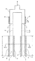
図1〜図3は、本発明のシリコン製造用反応装置の基本的な態様の一部を示す概略図であり、図4は、本発明のシリコン製造用反応装置の代表的な実用態様を示す概略図である(図1〜図3、図4とも該反応装置を縦断面視したときの図である)。また、図5〜図9は、本発明のシリコン製造用装置の上下方向に延在する壁によって囲まれた空間を、横断面視したときの代表的な形状の図面である。例えば、図1、図3に示されているシリコン製造用反応装置において、(E)−(E')面にて切断した場合の形状が、図7、図8、図9等で示され、同様に図2において、(E)−(E')面にて切断した場合の形状が、図6で示される。
【0010】
本発明のシリコン製造用反応装置を、図1を例に説明する。本発明のシリコン製造用反応装置は、反応容器1を構成する上下方向に延在する壁aにより囲まれた空間4にシリコン析出用原料ガスA(以下「原料ガス」と記載することがある)を流通させ、壁aの空間4に面する加熱された表面でシリコンを析出・溶融せしめ、下端の開口部2よりこれを落下せしめる構造を有する。
【0011】
本発明のシリコン製造用反応装置において、反応容器1の空間4が、横断面視でスリット形状を成すことが重要である。
即ち、本発明のシリコン製造用反応装置は、反応容器1の空間4が、横断面視でスリット形状を成すことにより、壁aの空間4に面する加熱された表面から大きく離れた空間を少なくする。つまり、上記壁aの表面と、原料ガスが上記壁aの表面と接触しにくい空間との距離を短くし、原料ガスの反応率を高め、かつ、副生成物の発生を抑制し、シリコンの生産効率を大幅に向上することができる。
【0012】
本発明において、反応容器1の空間4が、横断面視でスリット形状を成すことによる効果を、原料ガスが接触可能な部分の表面積が同一であって、反応容器1の空間4が、横断面視で幅(SD)と長さ(LD)が等しいもの、例えば、円状、正多角形状等のものと比較すると、該反応容器1の空間4が、横断面視でスリット形状のものは、壁aの空間4に面する加熱された表面から大きく離れた空間が少なくなるため、原料ガスが該壁の表面に接触する確率を高くすることができ、原料ガスの反応率を高めることができる。更に、原料ガスを上記壁aの表面に接触し易くした結果、上記空間4の原料ガスの温度を全体的に、十分に高くすることができ、副生成物が生成し易い温度領域を狭めることが可能となり、シリコンの収率も高めることができる。
【0013】
ここで原料ガスの反応率とは、反応容器1の空間4に供給した原料ガスが、該空間4から排出されるまでの間に何らかの物質に転化した割合で定義される。またシリコンの収率とは、上記の反応して何らかの物質に転化した原料ガスのうち、シリコンへ転化したものの割合で定義される。
【0014】
また、同一のガス供給量で反応を実施する場合、反応容器1の空間4が、横断面視でスリット形状を成すものは、原料ガスの流速が速まり、該空間4内に原料ガスが滞在する時間が短くなるが、後述する原料ガスの滞在時間内においては、原料ガスの滞在時間が短くなっても、原料ガスの反応率が低下しない。これは即ち、本発明のシリコン製造用反応装置においては、従来のシーメンス法と比較して、高い析出表面温度でシリコンの析出を実施することができ、かつ、原料ガスも十分に昇温されて活性化されるため、原料ガスが、壁aの空間4に面する加熱された表面と接触した際に、極めて短時間でシリコンへ転化する効果が発揮されるためであると考えられる。
【0015】
本発明において、反応容器1の空間4が、横断面視でスリット形状を成すことによる効果を、同一容積であって、反応容器1の空間4が、横断面視で幅(SD)と長さ(LD)が等しいもの、例えば、正多角形状、円状等のものと比較すると、同一のガス供給量で反応を実施する場合には、原料ガスが該空間4内に滞在する時間は同じになるが、反応容器1の空間4が、横断面視でスリット形状のものは、ガス供給量あたりのシリコンの析出が可能な部分の表面積を大きくすることができるため、原料ガスの反応率を高めることができ、同一規模の反応装置でも効率良く生産性を向上させることができる。
【0016】
また、反応容器1の空間4が、横断面視でスリット形状を成しているものをスケールアップすることにより、上述した効果に加え、壁aの空間4に面する加熱された表面の上下両端部での輻射熱損失を効果的に防止し、加熱エネルギーを大幅に節減しうる効果も得ることができる。すなわち、本発明のシリコン製造用反応装置を用いると、壁aの空間4に面する加熱された表面を互いに近接させて開口部の面積を小さくすることができる。そのため、外部への輻射損失が大幅に低減すると共に該表面の上下両端部の温度低下も効果的に抑制し、少ない加熱エネルギーで反応部の均質な温度分布を得ることができる。この効果は、輻射エネルギーが大きくなる1000℃以上の高温条件で実施する本発明の実施においては特に有効である。
【0017】
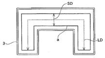
本発明において、上記スリット形状は、スリットが扁平形状のもの、スリットが周方向に連続した環状のものを含む。また、上記スリット形状の幅は、長手方向に対して一定であってもよいし、変化してもよいし、それらの組み合わせであってもよい。スリット形状の幅が一定のものを例示すると、図6に示すような環状のもの、図9に示すような直方体状のもの、図示はしていないが、直方体が湾曲したC字型のもの等が挙げられる。スリット形状の幅が変化するものを例示すると、図7に示すような楕円状のもの、図示はしていないが、菱形状のもの、三角形状のもの等が挙げられる。さらにそれらの組み合わせとして、図8に示すような直方体の四隅が円弧状のもの等が挙げられる。これら以外のものとしては、スリット形状が、図5に示すような直方体を組み合わせたコの字型のもの、図示はしていないが、L字型、T字型、十字型、星型のもの等、その他、曲線的な形状のもの、波状のもの等をあげることができる。
【0018】
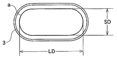
また、上記スリット形状の幅(SD)、長さ(LD)の決定例を図5〜図9に示す。スリットの長さ(LD)は、一般にスリット内の長手方向の最長距離を示す。一方、スリットの幅(SD)は、スリットの長さ(LD)よりも短い関係にあり、スリット形状において幅が一定である場合には、幅(SD)は壁と壁との間の距離を示す。また、長手方向に対して幅(SD)が変化する形状の場合には、幅(SD)は、長手方向を示す直線(LD線)に対するスリット内の垂線の最大長さとして定義される。一方、スリット形状が、屈曲または湾曲している場合には、対向する壁同士の最短距離を示す線分の中点を結ぶことで定義される直線または曲線の長さをLDとする。
【0019】
たとえば、図5では、幅(SD)は、壁と壁との間の距離であり、長さ(LD)は、対向する壁の中間を通るコの字型の線の長さである。また、図示はしていないが、T字型の場合も、幅(SD)は、壁と壁との間の距離であり、長さ(LD)は、対向する壁の中間を通るT字型の線の長さであり、十字型の場合も同様である。
【0020】
図6では、幅(SD)は、内側の壁a'と外側の壁aとの距離であり、長さ(LD)は、内側の壁a'と外側の壁aとの中間を通る円の円周である。
図8では、幅(SD)は、LD線に対するスリット内の垂線の最大長であり、長さ(LD)は、長手方向の最長距離である。
【0021】
図9では、幅(SD)は、壁と壁との間の距離であり、長さ(LD)は、長手方向の最長距離である。
また、図7に示すように反応容器の横断面視形状が楕円状である場合には、幅(SD)は短径を示し、長さ(LD)は長径を示す。
【0022】
さらに、図示はしていないが、菱形の場合は、幅(SD)は、最短対角線長であり、長さ(LD)は最長対角線長である。また三角形の場合は、長さ(LD)は最長辺であり、幅(SD)は最長辺と対角との距離である。
【0023】
本発明のシリコン製造用反応装置において、上記スリット形状の幅(SD)に対する長さ(LD)の比(LD/SD)は、1.5以上であることが好ましい。LD/SDの比が1.5未満の場合は、原料ガスの反応率の改良効果が顕著に発揮されない傾向にある。一方、LD/SDの上限は、特に制限されるものではないが、反応装置の製作上、LD/SD=1000以下であることが好ましい。尚、上記スリット形状は、上記効果と反応装置の製作を勘案するとLD/SDは、2〜400が好ましく、更に3〜300であることが好ましい。
【0024】
また、上記スリット形状の幅(SD)は、0.1m以下であることが好ましい。SDが0.1mを超える場合は、原料ガスの反応率の改良効果が顕著に発揮されない傾向にある。一方、SDの下限は、特に制限されるものではないが、反応装置の製作上、SDが0.005m以上であることが好ましい。上記効果と反応装置の製作を勘案するとSDは0.01〜0.08mが好ましく、更に0.01〜0.06mであることが好ましい。
【0025】
上記スリット形状のLD、およびSDの関係において、シリコンを工業的に生産するためには、該スリット形状の長さ(LD)は、0.15m以上であることが好ましい。一方、LDの上限は、特に制限されるものではないが、反応装置の製作上、LDが5m以下であることが好ましい。すなわち、シリコンの生産量と反応装置の製作を勘案するとLDは0.16〜4mが好ましく、更に0.18〜3mであることが好ましい。
【0026】
本発明のシリコン製造用反応装置において、反応容器1の空間4の縦断面視における形状は、特に制限されるものではないが、製作を容易にするために、図1〜図3に示すような直胴状にすることもできるし、開口部2に向かって徐々に径が減少するように絞り部を形成した態様等をとることができる。
【0027】
また、反応容器1の空間4の下端における開口部2は、その周縁が水平となるように構成する態様でも問題なく粒子状のシリコンを得るが、周縁が傾斜するように構成する態様、周縁を波状に構成する態様とすることもできる。
【0028】
更に、上述した開口部2の周縁の形状において、シリコンを融液として回収する場合は、溶融シリコンが壁aより落下する時の液切れを良くするため、先端部に向かって肉厚が次第に薄くなる刃物状にすることがより好ましい態様である。
【0029】
本発明のシリコン製造用反応装置において、上記スリット形状のLD/SDの比、SD、LD値は、反応容器1の空間4が縦断面視で、上述の通り、変化する態様をとる場合、原料ガスが壁aの空間4に面する表面と接触してシリコンの析出が可能な領域(以下「反応部I」と記載することがある)における平均値で示すものである。即ち、スリット形状のLD/SDの比、SD、LD値は、図1〜図3の反応部Iの最上部から最下端部の空間4における平均値で示すものである。尚、図1〜図2に示す通り、原料ガス吹き出し口6の位置が、加熱手段3の最上部の位置よりも上方にある場合には、反応部Iの最上部の位置は、加熱手段3の最上部の位置と同じものとする。また、図3に示す通り、原料ガス吹き出し口6の位置が、加熱手段3の最上部の位置と同じ位置、または下方にある場合には、反応部Iの最上部の位置は、原料ガス吹き出し口6の位置と同じものとする。
【0030】
本発明のシリコン製造用反応装置は、反応容器1における上下方向に延在する壁aが、空間4に面する表面において、下端部を含む少なくとも一部分の表面をシリコンの融点以上に加熱することが重要である。上記壁aの空間4に面する表面において、シリコンの融点以上に加熱する範囲は、下端部が含まれれば、特に制限されるものではなく、原料ガスの供給量、速度等を考慮して適宜決定してやればよいが、シリコンが析出する壁の表面全体(反応部I)をシリコンの融点以上に加熱できるように対応にしてやればよい。そのためには、上記シリコンの融点以上に加熱する範囲が、上下方向に延在する壁aの全長に対して、下端部から90%以下、好ましくは、80%以下の範囲にすることにより、反応容器1の上部におけるシリコンのスケール付着を防止することが容易となるため好ましい。また、上記シリコンの融点以上に加熱する範囲の下限は、上下方向に延在する壁aの全長に対して、シリコンの生産量を確保するためには、下端部から20%以上、好ましくは、30%以上の範囲である。
【0031】
本発明のシリコン製造用反応装置において、原料ガス供給管5は、反応容器1の空間4の上部から下部に原料ガスを流通させるためのものであり、原料ガス供給管5の原料ガス吹き出し口6の位置は、図1〜図2に示す通り、壁aの空間4に面する表面をシリコンの融点以上に加熱する領域の最上部、反応部Iの最上部よりも上方に設けることもできるし、図3に示す通り、上記反応部Iの最上部の位置と同じか、それよりも下方に設けることもできる。
【0032】
本発明において、図1〜図2に示す通り、原料ガス供給管5の原料吹き出し口6の位置を、壁aの空間4に面する表面をシリコンの融点以上に加熱する領域の最上部、反応部Iの最上部よりも上方に設けた場合には、原料供給管5によって奪われる熱が少なくなって、加熱手段3のエネルギー効率を向上させることができる。この場合、シリコンを溶融・析出させる方法としては、反応部Iにおける壁aの空間4に面する表面をシリコンが析出可能な温度に設定し、一度シリコンを析出させた後、上記表面をシリコンの融点以上に設定し、析出したシリコンを溶融落下させる方法を用いることができる。
【0033】
上記シリコンを溶融・析出させる方法において、加熱手段3の制御方法としては、壁aの空間4に面する表面を上部、下部の二段、またはそれ以上の複数段に分けて、各段の温度制御を行なうことが好ましい。具体的な加熱手段3の制御方法としては、シリコンの析出反応中に主として使用する第一の加熱手段と、伝熱によって壁aの空間4に面する表面が昇温されてシリコンが析出する部分を加熱する第二の加熱手段の少なくとも二段以上に分割し、それぞれ加熱出力が調整可能な加熱手段を設けて制御することが好ましい。即ち、第二の加熱手段は、シリコンの析出反応中には出力を低く、あるいはゼロに設定しておき、シリコンを溶融させる場合に出力を上昇させてシリコンを落下させることにより、反応容器1内のシリコンのスケール成長を防止することが可能となる。
【0034】
また、上記のシリコンを溶融・析出させる方法において、反応容器1内のシリコンのスケール付着物を除去する方法としては、上記の加熱手段3を制御する方法の他に、塩化水素などのエッチング性ガスを間欠的に供給して、スケール付着物を反応除去する方法も採用することができ、またこれらを組み合わせた方法を採用することも可能である。
【0035】
本発明において、図3に示す通り、原料ガス供給管5の原料吹き出し口6の位置を、反応部Iの最上部と同じ位置、または下方に設けた場合、シリコンを析出・溶融させる方法は、反応部Iにおける壁aの空間4に面する表面をシリコンの融点以上の温度に設定して、シリコン融液を連続的に落下させる方法、または該表面をシリコンが析出可能な温度に設定し、一度シリコンを析出させた後、該表面をシリコンの融点以上に設定し、析出したシリコンを溶融落下させる方法等を用いることができる。尚、この場合は、後述の通り、上下方向に延在する壁aと原料ガス供給管5の空間において、供給されたシリコン原料が、シリコンが固体状で析出する低温領域となる部分でのシリコンの析出・成長が起こるのを防止するため、該低温領域にシールガスを供給(シールガスC、シールガス供給管8)することが好ましい。
【0036】
上記シリコンを溶融・析出させる方法において、加熱手段3の制御方法としては、シリコンの析出に関与する壁の表面全てを同一温度に制御しても良いし、該表面を上部、下部の二段、またはそれ以上の複数段に分けて、各段の温度制御を行なうこともできる。また、上記温度制御は、反応容器1の加熱手段3全てを同一のもので行なっても良いし、複数段に各加熱手段を設けて制御することもできる。
【0037】
本発明のシリコン製造用反応装置において、加熱手段3は、壁aの空間4に面する表面をシリコンの融点以上に加熱することができるものであれば、公知の手段が特に制限なく採用される。ここで、シリコンの融点は1410〜1430℃の範囲にあると考えられている。具体的な加熱手段は、外部からのエネルギーにより壁aの空間4に面する表面を加熱する手段が挙げられ、より具体的には、高周波による加熱方法、電熱線を用いる加熱手段、赤外線を用いる加熱手段等が挙げられる。
【0038】
これらの方法のうち、高周波を用いる加熱方法は、高周波を放出する加熱コイルの形状をシンプルにしながら、壁aの空間4に面する表面を均質的な温度に加熱することが容易にできるため、好適に使用される。
【0039】
また、本発明のシリコン製造用反応装置において、高周波を加熱手段に用いる場合には、加熱のエネルギー効率を向上させるために、壁aと加熱手段3との間に断熱材を挿入することも可能である。
【0040】
本発明のシリコン製造用反応装置において、装置の規模に対して、シリコンの析出に関与する壁aの表面積を有効に広げるためには、上記反応容器1の空間が、横断面視で図6に示すような環状の形態をとることが好ましい。この場合には、内側に配置された壁a'の空間4に面する表面を十分に加熱するために、図2、図6に示す通り、加熱手段3'を設けることも可能である。
【0041】
また、その他の加熱方法として、外側の壁aを肉厚10mm以下のカーボン繊維強化炭素複合材料を用い、また内側の壁a'に一般的な等方性のカーボンを用いる態様とすることにより、外側に配置された高周波等の加熱手段3のみで、外側の壁aと内側の壁a'の空間に面する両表面を同時に加熱することもできる。即ち、外側の壁aを構成するカーボン繊維強化炭素複合材料は、一般的な等方性カーボンと比較して、強度が高く薄肉化ができること、および電気伝導率が低いために、加熱手段3から高周波エネルギーを適度に透過させることができ、内側の壁a'の空間4に面する表面に十分な加熱エネルギーを供給することが可能となる。
【0042】
本発明のシリコン製造用反応装置において、上記原料ガス供給管5の形状は、特に限定されるものではなく、円筒状のものであってもよいし、その横断面視でスリット形状のものであってもよく、これらのものを反応容器1の空間4の横断面視における、スリット形状の長さ方向に複数本並列に配置して使用することもできる。中でも、原料ガスを空間4内により均一に分散させるためには、原料ガス供給管の形状は、円筒状のものを上記スリット形状の長さ方向に複数本並列に配置させるか、または、原料ガス供給管の横断面視の形状が、反応容器1の空間4の横断面視の形状と相似であることが好ましい。
【0043】
また、原料ガス供給管5は、該供給管の熱劣化を防止し、後に詳述する原料ガスである各種シラン類が分解するのを防ぐため、該供給管を冷却する冷却手段を備えることが好ましい。冷却手段7の具体的態様は、特に制限されず、図1〜図3に示すような、原料ガス供給管の内部に水、熱媒油等の冷媒液体をD1から供給し、D2より排出するようにした流路を設けて冷却する液体ジャケット方式、図示されてはいないが、原料ガス供給管に多重環ノズルを設けることによる空冷ジャケット方式等が挙げられる。
【0044】
原料ガス供給管5の冷却温度は、供給管を構成する材質が著しく劣化しない程度に冷却すればよく、一般には、供給する原料ガスの自己分解温度未満に設定してやればよい。
【0045】
また、原料ガス供給管5の材質としては、後述する上下方向に延在する壁aと同様の材質の他、鉄およびステンレス鋼等も使用することができる。
以下、本発明のシリコン製造用反応装置の実用態様の例を図4の例を用いて説明する。
【0046】
本発明のシリコン製造用反応装置の他の構造は、公知の構造、例えば、特開2002−29726号公報などに記載された構造が特に制限無く採用される。
具体的には、図4に示すように反応容器1は、排ガスGの排ガス排出管9を接続した密閉容器10中に設けられ、外気と遮断することにより、純度の高いシリコンを得ることができ、さらに排ガスを効率よく回収することができる。また、上記密閉容器10は、下部に冷却室を設けてもよい。この冷却室には、開口部2から落下したシリコン15を回収する室が形成される。また、密閉容器10には上記排ガス排出管9の他、冷却媒体をF1からF2、F3からF4に流通させる冷却ジャケット13、該ジャケットにより冷却される冷却空間14を設けてもよい。さらに、下部の冷却室には得られたシリコン15を冷却する冷却ガスHを供給する冷却ガス供給管12を設けることもできる。また、冷却空間14中に仕切り板16を設け、生成したシリコン15を取出口17から取り出す態様にすることもできる。
【0047】
また、上記の通り、原料ガス吹き出し口6の位置が、壁aの空間4に面する表面をシリコンの融点以上に加熱する領域の最上部と同位置、または下方にある場合には、該壁aと原料ガス供給管5の空間において、供給されたシリコン原料が、シリコンが固体状で析出する低温領域となる部分でのシリコンの析出・成長が起こるのを防止するため、該低温領域にシールガスを供給(シールガスC、シールガス供給管8)することが好ましい。このシールガスは、シリコンの製造に悪影響を与えないガスが好適であり、具体的にはアルゴン、ヘリウム等の不活性ガスや水素が好適であり、排ガスを循環して使用する場合には、特に水素が好適である。また、反応容器1と密閉容器10の空間においても、シリコンの析出を防ぐため、シールガス供給管11から、上記シールガスを供給することが好ましい。
【0048】
更に、シールガスの効果を高めるために、シリコンをエッチングし得るガス、例えば塩化水素などをシールガスに適宜混合することもより好ましい態様である。
【0049】
本発明において、反応容器1の上下方向に延在する壁aは、シリコンの融点以上に加熱され、その内部は各種シラン類やシリコン溶融液に接触するため、これらの温度条件や接触物に対して十分に耐える材質を選択することが長期間の安定したシリコンの製造を行う上で望ましい。
【0050】
かかる材質としては、例えば、グラファイト、熱分解炭素、カーボン繊維強化炭素複合材料等の炭素材料、炭化ケイ素(SiC)、窒化ケイ素(Si3N4)、および窒化ホウ素(BN)、窒化アルミ(AlN)等のセラミックス材料の、単独材料または複合材料が挙げられる。
【0051】
これら材質のうち、炭素材料を基材とする場合、析出するシリコンの汚染を防ぐために、少なくともシリコン溶融液と接触する部分を熱分解炭素、Si3N4、SiCを被覆することが好ましい。
【0052】
本発明のシリコン製造用反応装置において、原料ガス供給管5より供給される原料ガスは、公知のシリコン原料ガスとして使用される各種シラン類が挙げられる。具体的には、トリクロロシラン(TCS)、四塩化ケイ素(STC)、モノシラン、ジクロロシランなどが挙げられる。中でもモノシランやTCSが工業的に高純度のものを大量に入手可能であるために好ましい。また、上記原料ガスは希釈して使用することもでき、この希釈ガスは、上記シールガスと同様、シリコンの製造に悪影響を与えないガスが好適である。特に未反応の原料ガスを循環して使用する場合には、該希釈ガスは水素が好ましく、原料ガスの希釈する割合は、原料ガスが1〜30モル%、好ましくは3〜20モル%の割合にすることが好ましい。この希釈ガスを使用する場合は、予め原料ガスを希釈して、上記原料ガス供給管から供給してもよいし、原料ガスとは別に希釈ガスの供給管を設けて供給することもできる。
【0053】
本発明のシリコン製造用反応装置において、壁aの空間4に面する表面でシリコンを析出・溶融させる温度は、使用する原料ガスの組成や、シリコン溶融・析出方法等により適宜決定してやればよい。中でも高純度の安定したシリコンを得るためには、原料ガスにTCSを使用して、上記壁の表面を1300℃〜1700℃の温度でシリコンの析出・溶融を行うことが好ましい。本発明のシリコン製造用反応装置において、壁aの空間4に面する表面を1300℃〜1700℃という高温でシリコンの析出・溶融を行うことにより、該壁aによって囲まれた空間4が、横断面視で、スリット形状を成すことの効果が顕著に発揮される。
【0054】
本発明のシリコン製造用反応装置において、原料ガスを反応させる圧力は、工業的な生産が可能であり、安定した生産を確保できる範囲であれば、特に制限されるものでなく、常圧から3MPaG、好ましくは常圧〜1MPaGである。
【0055】
本発明のシリコン製造用反応装置において、各種ガスの滞在時間は、一定容量の筒状容器に対して、反応時の温度、圧力等の条件によって適宜調整してやればよいが、平均的な滞在時間は0.001〜60秒、好ましくは0.01〜10秒、更に好ましくは0.05〜1秒である。この範囲に設定することにより、十分に経済的な原料ガスの反応率を得ることが可能となる。
以下、本発明を詳細に説明するための実施例を挙げて説明するが、本発明はこれらの実施例に限定されるものではない。
【実施例】
【0056】
[実施例1]
反応容器1は、上下方向に延在する壁aがグラファイト製で、該壁によって囲まれた空間4が、横断面視で図8に示すような扁平形状を示し、そのSDが0.1m、LDが0.16m、肉厚が15mm、長さが1.0mの直胴状であり、下部に開口部2を有するものを使用した。原料ガス供給管5は、ステンレス製で冷却手段7として通液可能なジャケット構造を有してなり、原料ガス吹き出し口6が10mm×100mmのスリット状のものを使用した。
【0057】
なお、原料ガス供給管5は、原料ガス吹き出し口6の中心と長径方向が、上記空間4の扁平形状のそれらと一致するようにし、原料ガス吹き出し口6の高さは、図3の反応部Iの長さが0.6mになるように、上記反応容器1に設置した。また、反応部Iにおける壁aの空間4に面する表面をシリコンの融点以上に加熱しうるように、加熱手段3として、周波数8kHzの高周波を発生する(加熱法)加熱コイルを壁aの上端から0.3m下の位置から下端より更に0.1m下の位置まで反応容器1を取り囲む形で設置した。尚、断熱材として、厚み50mmのカーボン繊維性断熱材を、壁aの上端から0.2m下の位置から下端より0.03m上の位置まで反応容器1と加熱手段3を取り囲む形状で設置した。また、密閉容器10はステンレス製で内径1m、長さ1.5mのものを使用した。
【0058】
原料ガス供給管5、密閉容器10を通水によって冷却し、シールガス供給管8、シールガス供給管11から水素ガスをそれぞれ5Nm3/Hで流通させながら、高周波加熱手段3により壁aの空間4に面する表面を1500℃に加熱した。
原料ガス供給管5からトリクロロシランと水素を、それぞれ35kg/H、100Nm3/Hの速度で供給したところ、シリコンを約1.3kg/Hで安定的に得ることができた。このときのトリクロロシランの反応率は約35%であった。このとき、微粉状シリコンの発生は少量であり、シリコンの収率も向上した。この結果を表1にまとめた。
【0059】
[実施例2]
実施例1において、上下方向に延在する壁aによって囲まれた空間4が、横断面視でSDを0.04m、LDを0.2mの扁平形状に変更し、原料ガス供給管5は、原料ガス吹き出し口6を10mm×170mmのスリット状に変更し、これに応じて加熱手段3の高周波加熱コイルの形状も、厚み50mmの断熱材を介して該反応容器1を取り囲む形状に変更した。上記以外は、実施例1と同様の装置を用いながら同様の条件で反応を行った。結果を表1にまとめた。このとき、微粉状シリコンの発生は極めて少なかった。
【0060】
[実施例3]
実施例2において、上下方向に延在する壁aに囲まれた空間4が横断面視でSDを0.04m、LDを1mの扁平形状に変更し、またこれに応じて加熱手段3の高周波加熱コイルの形状も相応に変更した。さらに原料ガス吹き出し口6も10mm×970mmのスリット状に変更した。密閉容器10も内面が、横断面視で図8に示すような扁平形状とし、その短径が0.5m、長径が3mとなるように変更し、該扁平形状の向きは、上記空間4の扁平形状と同じにした。
【0061】
シールガス供給管8、シールガス供給管11から水素ガスをそれぞれ25Nm3/Hで流通させ、原料ガス供給管5からはトリクロロシランと水素を、それぞれ175kg/H、500Nm3/Hの速度で供給して反応を行った。結果を表1にまとめた。このとき、微粉状シリコンの発生は極めて少なかった。
【0062】
[実施例4]
外側の壁aはカーボン繊維強化炭素複合材料製で内径0.25m、肉厚を5mmとし、内側の壁a'は汎用の等方性グラファイト製で内径0.2m、肉厚を15mmのものを使用した。反応容器1は、壁aと壁a'によって囲まれた空間4が、横断面視で図6に示すような円状を示し、そのSDが0.025m、LDが0.71m、長さが1mの直胴状であり、下部に開口部2を有するものを使用した。
【0063】
原料ガス供給管5はステンレス製で、冷却手段7として通液可能なジャケット構造を有しながら、反応容器1の上部をすべて覆いかぶせるように配置した。このとき、内側の壁a'の上端は同様の材質で蓋状に閉塞させているため、結果として原料ガス吹き出し口6の位置は、壁aと壁a'の最上端の位置と一致している。
【0064】
また、壁aと壁a'の空間4に面する表面で原料ガスが接触可能な部分を、シリコンの融点以上に加熱しうるように、加熱手段3としての周波数1kHzの高周波を発生する加熱コイルを壁aの上端から0.15m下の位置から下端よりさらに下に0.1mの位置まで外側の壁aを取り囲む形で設置した。
【0065】
なお厚み50mmのカーボン繊維性断熱材を外側の壁aの最上端部から下端より0.03m上の位置まで外側の壁aと該加熱コイルの間、および内側の壁a'の閉塞させている上端部蓋のさらに上部に設置した。また、密閉容器10はステンレス製で内径1m、長さ1.5mのものを使用した。
【0066】
原料ガス供給管5、密閉容器10を通水によって冷却し、高周波加熱手段3により壁aおよび壁a'の空間4に面する両表面の温度が1300〜1400℃になるように加熱した。
【0067】
原料ガス供給管5からトリクロロシランと水素を、それぞれ175kg/H、500Nm3/Hの速度で供給して反応を行った。このとき、2時間原料ガスを上記供給量で供給し、その後15分間原料ガス供給量を1/3に絞る操作を繰り返すと、ガス供給量を絞った際にシリコンが溶融して落下した。結果を表1にまとめた。このとき、微粉状のシリコンの発生は極めて少なかった。
【0068】
[比較例1]
上下方向に延在する壁aによって囲まれた空間4が、横断面視で内径0.15mの円状を示し、反応部Iの長さを0.6mとし、原料ガス吹き出し口も40mmの円状とした。またこれに応じて加熱手段3としての高周波加熱コイルの形状も厚み50mmの断熱材を介して該反応容器を取り囲む形状に変更した。上記以外は、実施例1と同様の装置を用いながら同様の条件で反応を行った。結果を表1にまとめた。このとき、微粉状シリコンの発生は、やや多く見られた。
【0069】
[比較例2]
上下方向に延在する壁aに囲まれた空間4が、横断面視で内径0.23mの円状を示し、反応部Iの長さを0.6mとし、原料ガス吹き出し口も60mmの円状とした。またこれに応じて加熱手段3としての高周波加熱コイルの形状も厚み50mmの断熱材を介して該反応容器を取り囲む形状に変更した。上記以外は、実施例3と同様の装置を用いながら同様の条件で反応を行った。結果を表1にまとめた。このとき、微粉状シリコンの発生は、やや多く見られた。
【表1】

表1に示す通り、実施例1、2と比較例1を比較すると、反応容器において、シリコンの生成に関与する部分の表面積が同程度の場合には、実施例1、2は、原料ガスの滞在時間が短いにもかかわらず、原料ガスの反応率がよく、加えて好ましくない微粉の発生量も低減でき、シリコンの収率がよいことがわかる。
【0071】
また、実施例3と比較例2を比較すると、反応容器において、容積が同程度であって、ガスの滞留時間を同程度にした場合でも、実施例3は、原料ガスの反応率がよく、シリコンの生産量を大幅に向上させることができた。
【0072】
本発明のシリコン製造用反応装置を用いると、反応容器をスケールアップした場合においても、原料ガスの高い反応率を維持し、シリコンの生産量をきわめて効率よく増大することができた。
【0073】
以上の説明より理解されるように、本発明のシリコン製造用反応装置は、シリコンを長期間連続して製造する反応装置をスケールアップする場合において、原料ガスの反応率を高めることができ、かつ、副生成物の生成を抑制することによって、シリコンの収率を高く維持し、生産効率を大幅に向上させた。更に、上下方向に延在する壁によって囲まれた空間の両端部での輻射熱損失を効果的に防止できた。
【図面の簡単な説明】
【0074】
図1は、本発明のシリコン製造用反応装置の基本的な態様の一部を示す概略図であって、該反応装置を縦断面視したときの図を示したものである。
図2は、本発明のシリコン製造用反応装置の基本的な態様の一部を示す概略図であって、該反応装置を縦断面視したときの図を示したものである。
図3は、本発明のシリコン製造用反応装置の基本的な態様の一部を示す概略図であって、該反応装置を縦断面視したときの図を示したものである。
図4は、本発明のシリコン製造用反応装置の代表的な実用態様を示す概略図であって、該反応装置を縦断面視したときの図を示したものである。
図5は、本発明のシリコン製造用装置の上下方向に延在する壁によって囲まれた空間を横断面視したときの代表的な図を示したものである。
図6は、本発明のシリコン製造用装置の上下方向に延在する壁によって囲まれた空間を横断面視したときの代表的な図を示したものである。
図7は、本発明のシリコン製造用装置の上下方向に延在する壁によって囲まれた空間を横断面視したときの代表的な図を示したものである。
図8は、本発明のシリコン製造用装置の上下方向に延在する壁によって囲まれた空間を横断面視したときの代表的な図を示したものである。
図9は、本発明のシリコン製造用装置の上下方向に延在する壁によって囲まれた空間を横断面視したときの代表的な図を示したものである。
【符号の説明】
【0075】
1 ;反応容器
2 ;開口部
3 ;加熱手段
3';加熱手段
4 ;空間
5 ;原料ガス供給管
6 ;原料ガス吹き出し口
7 ;冷却手段
8 ;シールガス供給管
9 ;排ガス排出管
10 ;密閉容器
11 ;シールガス供給管
12 ;冷却ガス供給管
13 ;冷却ジャケット
14 ;密閉容器の冷却空間
15 ;シリコン
16 ;仕切り板
17 ;シリコン取出口
A ;シリコン析出用原料ガス
C ;シールガス
I ;反応部
a ;壁
a' ;壁【Technical field】
[0001]
The present invention relates to a novel reactor for the production of silicon. Specifically, when silicon is produced industrially continuously for a long period of time, the reaction rate of the source gas can be increased, and by suppressing the production of by-products, the yield of silicon can be maintained high. The present invention relates to a reactor for producing silicon that can improve production efficiency.
[Background]
[0002]
Conventionally, various methods for producing silicon used as a raw material for semiconductors or photovoltaic power generation batteries are known, some of which have already been industrially implemented.
[0003]
For example, one of them is a method called a Siemens method, in which a silicon rod heated to a silicon deposition temperature by energization is placed inside a bell jar, and trichlorosilane (SiHCl) is placed therein. Three Hereafter referred to as TCS) and monosilane (SiH Four ) In contact with a reducing gas such as hydrogen to deposit silicon.
[0004]
This method is characterized in that high-purity silicon can be obtained, and is implemented as the most general method, but since precipitation is batch-type, the installation of a silicon rod as a seed, the current heating of the silicon rod, There is a problem that extremely complicated procedures such as precipitation, cooling, taking out, and cleaning of a bell jar must be performed.
[0005]
In response to the above problem, Japanese Patent Application Laid-Open No. 2002-29726 discloses a reaction apparatus capable of continuously and stably producing silicon over a long period of time in a cylindrical container that can be heated to a temperature higher than the melting point of silicon. A reactor for producing silicon that supplies raw material gas for precipitation and deposits silicon by heating the cylindrical container, and continuously melts and drops the deposited silicon from the lower end of the cylindrical container. Proposed.
[0006]
The above reaction apparatus solves various problems of the conventional Siemens method and is an extremely excellent apparatus capable of continuously producing silicon. However, in order to produce silicon on an industrial scale of several hundred tons or more per year, when the reaction vessel such as the cylindrical shape shown in the examples of JP-A-2002-29726 is scaled up as it is, The reaction rate of the raw material gas decreases. Further, by-products such as silicon fine powder and low molecular weight polymers of silane compounds are likely to be generated, and the yield of silicon tends to decrease, and improvement has been desired.
DISCLOSURE OF THE INVENTION
[Problems to be solved by the invention]
[0007]
The inventors of the present invention have made extensive studies to solve the above problems. As a result, in the said apparatus, the knowledge that the cause of the said subject originates in the cross-sectional view shape of a cylindrical container inner surface was acquired. That is, when the reactor whose inner surface of the cylindrical container has a simple circular shape, regular polygonal shape, etc. in a cross-sectional view is scaled up, there is a space greatly separated from the heated inner surface of the cylindrical container, and the source gas Problems such as a decrease in the reaction rate and the ease of forming by-products arise. As a result of repeated studies based on such knowledge, in a reaction vessel composed of a wall extending in the vertical direction and a space surrounded by the wall, the space of the reaction vessel forms a slit shape in a cross-sectional view. Therefore, the space greatly separated from the surface facing the space of the wall is reduced, that is, the distance between the surface of the wall where silicon can be deposited and the space where the source gas is difficult to contact the surface of the wall is shortened. The inventors have found that all the above problems can be solved, and have completed the present invention.
[Means for Solving the Invention]
[0008]
That is, the present invention is to heat a reaction vessel in which a space surrounded by a wall extending in the vertical direction is formed and at least a part of the surface including the lower end portion of the wall facing the space to a temperature equal to or higher than the melting point of silicon. A reaction apparatus for producing silicon having a heating means capable of flowing a silicon deposition source gas from an upper part to a lower part of the space of the reaction container. A reactor for producing silicon characterized by having a slit shape.
【The invention's effect】
BEST MODE FOR CARRYING OUT THE INVENTION
[0009]
Hereinafter, the present invention will be described with reference to the accompanying drawings showing typical embodiments thereof, but the present invention is not limited to these accompanying drawings.
1 to 3 are schematic views showing a part of basic aspects of the reactor for producing silicon of the present invention, and FIG. 4 shows a typical practical embodiment of the reactor for producing silicon of the present invention. FIG. 1 is a schematic view (FIGS. 1 to 3 and FIG. 4 are views when the reaction apparatus is viewed in a longitudinal section). 5 to 9 are drawings of typical shapes when the space surrounded by the wall extending in the vertical direction of the apparatus for producing silicon of the present invention is viewed in cross section. For example, in the reaction apparatus for silicon production shown in FIGS. 1 and 3, the shape when cut along the (E)-(E ′) plane is shown in FIGS. 7, 8, 9, etc. Similarly, in FIG. 2, the shape when cut along the plane (E)-(E ′) is shown in FIG.
[0010]
The reaction apparatus for producing silicon according to the present invention will be described with reference to FIG. The reaction apparatus for producing silicon of the present invention has a silicon deposition source gas A (hereinafter sometimes referred to as “source gas”) in a space 4 surrounded by a wall a extending in the vertical direction constituting the
[0011]
In the reaction apparatus for producing silicon of the present invention, it is important that the space 4 of the
That is, in the reactor for producing silicon of the present invention, the space 4 of the
[0012]
In the present invention, the effect of forming the slit shape in the cross-sectional view of the space 4 of the
[0013]
Here, the reaction rate of the raw material gas is defined as the rate at which the raw material gas supplied to the space 4 of the
[0014]
Further, when the reaction is performed with the same gas supply amount, when the space 4 of the
[0015]
In the present invention, the effect obtained when the space 4 of the
[0016]
Further, by scaling up the space 4 of the
[0017]
In the present invention, the slit shape includes a flat slit and an annular shape in which the slit is continuous in the circumferential direction. The width of the slit shape may be constant with respect to the longitudinal direction, may vary, or may be a combination thereof. Examples of slits having a constant width include an annular shape as shown in FIG. 6, a rectangular parallelepiped shape as shown in FIG. 9, a C-shaped shape with a rectangular parallelepiped not shown, and the like. Is mentioned. Examples of those in which the width of the slit shape changes include an elliptical shape as shown in FIG. 7, a diamond shape, a triangular shape, etc., although not shown. Furthermore, as a combination thereof, a rectangular parallelepiped having four arcs as shown in FIG. Other than these, the slit shape is a U-shape with a combination of rectangular parallelepipeds as shown in FIG. 5, although not shown, L-shape, T-shape, cross shape, star shape In addition, a curved shape, a wavy shape, and the like can be given.
[0018]
Examples of determining the slit shape width (SD) and length (LD) are shown in FIGS. The length (LD) of the slit generally indicates the longest distance in the longitudinal direction in the slit. On the other hand, the slit width (SD) is shorter than the slit length (LD), and when the width is constant in the slit shape, the width (SD) is the distance between the walls. Show. Further, in the case of a shape whose width (SD) changes with respect to the longitudinal direction, the width (SD) is defined as the maximum length of a perpendicular line in the slit with respect to a straight line (LD line) indicating the longitudinal direction. On the other hand, when the slit shape is bent or curved, the length of a straight line or a curve defined by connecting the midpoints of the line segments indicating the shortest distance between the opposing walls is defined as LD.
[0019]
For example, in FIG. 5, the width (SD) is the distance between the walls, and the length (LD) is the length of a U-shaped line passing through the middle of the opposing walls. Although not shown, in the case of a T-shape, the width (SD) is a distance between the walls, and the length (LD) is a T-shape that passes through the middle of the opposing walls. This is also the case with the cross shape.
[0020]
In FIG. 6, the width (SD) is a distance between the inner wall a ′ and the outer wall a, and the length (LD) is a circle passing between the inner wall a ′ and the outer wall a. It is a circumference.
In FIG. 8, the width (SD) is the maximum length of the perpendicular in the slit with respect to the LD line, and the length (LD) is the longest distance in the longitudinal direction.
[0021]
In FIG. 9, the width (SD) is the distance between the walls, and the length (LD) is the longest distance in the longitudinal direction.
Moreover, as shown in FIG. 7, when the cross-sectional view shape of the reaction vessel is an ellipse, the width (SD) indicates the minor axis and the length (LD) indicates the major axis.
[0022]
Further, although not shown, in the case of a rhombus, the width (SD) is the shortest diagonal length, and the length (LD) is the longest diagonal length. In the case of a triangle, the length (LD) is the longest side, and the width (SD) is the distance between the longest side and the diagonal.
[0023]
In the reactor for producing silicon of the present invention, the ratio (LD / SD) of the length (LD) to the width (SD) of the slit shape is preferably 1.5 or more. When the ratio of LD / SD is less than 1.5, the effect of improving the reaction rate of the raw material gas tends not to be remarkably exhibited. On the other hand, the upper limit of LD / SD is not particularly limited, but it is preferable that LD / SD = 1000 or less in the production of the reaction apparatus. The slit shape is preferably from 2 to 400, and more preferably from 3 to 300, taking into account the above effects and the production of the reaction apparatus.
[0024]
The slit-shaped width (SD) is preferably 0.1 m or less. When SD exceeds 0.1 m, the effect of improving the reaction rate of the raw material gas tends not to be exhibited remarkably. On the other hand, the lower limit of SD is not particularly limited, but SD is preferably 0.005 m or more in the production of the reaction apparatus. Considering the above effects and the production of the reaction apparatus, the SD is preferably 0.01 to 0.08 m, and more preferably 0.01 to 0.06 m.
[0025]
In order to industrially produce silicon in the relationship between the slit-shaped LD and SD, the slit-shaped length (LD) is preferably 0.15 m or more. On the other hand, the upper limit of the LD is not particularly limited, but it is preferable that the LD is 5 m or less in the production of the reaction apparatus. That is, considering the production amount of silicon and the production of the reactor, the LD is preferably 0.16 to 4 m, and more preferably 0.18 to 3 m.
[0026]
In the reaction apparatus for producing silicon of the present invention, the shape of the space 4 of the
[0027]
In addition, the
[0028]
Furthermore, in the shape of the peripheral edge of the
[0029]
In the reactor for producing silicon of the present invention, when the slit-shaped LD / SD ratio, SD, and LD value are changed as described above when the space 4 of the
[0030]
In the reaction apparatus for producing silicon of the present invention, the wall a extending in the vertical direction in the
[0031]
In the reaction apparatus for producing silicon of the present invention, the source
[0032]
In the present invention, as shown in FIGS. 1 to 2, the position of the raw material outlet 6 of the raw material
[0033]
In the above method for melting and precipitating silicon, the heating means 3 is controlled by dividing the surface of the wall a facing the space 4 into upper, lower two or more stages, and the temperature of each stage. Control is preferably performed. As a specific control method of the heating means 3, there are a first heating means mainly used during the silicon precipitation reaction, and a portion where the surface of the wall a facing the space 4 is heated by heat transfer and silicon is precipitated. It is preferable that the second heating means for heating is divided into at least two stages and controlled by providing heating means capable of adjusting the heating output. That is, the second heating means sets the output to low or zero during the silicon precipitation reaction, and when the silicon is melted, the output is increased and the silicon is dropped, so that the inside of the
[0034]
In the method for melting and precipitating silicon, as a method for removing silicon scale deposits in the
[0035]
In the present invention, as shown in FIG. 3, when the position of the raw material outlet 6 of the raw material
[0036]
In the method for melting and precipitating silicon, the heating means 3 may be controlled by controlling all the surfaces of the walls involved in silicon precipitation at the same temperature, and the surface may be upper and lower two stages. Alternatively, the temperature control of each stage can be performed in a plurality of stages. The temperature control may be performed by using the same heating means 3 for the
[0037]
In the reaction apparatus for producing silicon of the present invention, as the heating means 3, any known means can be used without any limitation as long as the surface of the wall a facing the space 4 can be heated to the melting point of silicon or higher. . Here, the melting point of silicon is considered to be in the range of 1410 to 1430 ° C. Specific heating means include means for heating the surface of the wall a facing the space 4 by energy from the outside. More specifically, a heating method using a high frequency, a heating means using a heating wire, and infrared rays are used. A heating means etc. are mentioned.
[0038]
Among these methods, the heating method using a high frequency can easily heat the surface of the wall a facing the space 4 to a uniform temperature while simplifying the shape of the heating coil that emits the high frequency. It is preferably used.
[0039]
In the reaction apparatus for producing silicon of the present invention, when a high frequency is used for the heating means, a heat insulating material can be inserted between the wall a and the heating means 3 in order to improve the energy efficiency of the heating. It is.
[0040]
In the reaction apparatus for producing silicon according to the present invention, in order to effectively increase the surface area of the wall a involved in silicon deposition with respect to the scale of the apparatus, the space of the
[0041]
Further, as another heating method, by using a carbon fiber reinforced carbon composite material having a wall thickness of 10 mm or less for the outer wall a, and using a general isotropic carbon for the inner wall a ′, Both surfaces facing the space of the outer wall a and the inner wall a ′ can be simultaneously heated only by the high-frequency heating means 3 arranged on the outer side. That is, the carbon fiber reinforced carbon composite material that constitutes the outer wall a has higher strength and can be thinner than general isotropic carbon, and has low electrical conductivity. High frequency energy can be appropriately transmitted, and sufficient heating energy can be supplied to the surface of the inner wall a ′ facing the space 4.
[0042]
In the reaction apparatus for producing silicon of the present invention, the shape of the raw material
[0043]
The source
[0044]
The cooling temperature of the source
[0045]
Moreover, as a material of the source
Hereinafter, an example of a practical aspect of the reactor for producing silicon of the present invention will be described with reference to the example of FIG.
[0046]
As the other structure of the reaction apparatus for producing silicon of the present invention, a known structure, for example, a structure described in JP-A-2002-29726 is employed without any particular limitation.
Specifically, as shown in FIG. 4, the
[0047]
In addition, as described above, when the position of the source gas outlet 6 is at the same position as or below the uppermost portion of the region where the surface of the wall a facing the space 4 is heated to the melting point of silicon or higher, the wall In the space between a and the source
[0048]
Furthermore, in order to enhance the effect of the sealing gas, it is also a more preferable aspect that a gas capable of etching silicon, for example, hydrogen chloride is appropriately mixed with the sealing gas.
[0049]
In the present invention, the wall a extending in the vertical direction of the
[0050]
Examples of such materials include carbon materials such as graphite, pyrolytic carbon, and carbon fiber reinforced carbon composite materials, silicon carbide (SiC), and silicon nitride (Si Three N Four ), And a ceramic material such as boron nitride (BN) or aluminum nitride (AlN), or a single material or a composite material.
[0051]
Among these materials, when a carbon material is used as a base material, in order to prevent contamination of deposited silicon, at least a portion in contact with the silicon melt is decomposed into pyrolytic carbon and Si. Three N Four It is preferable to coat SiC.
[0052]
In the silicon production reactor of the present invention, examples of the source gas supplied from the source
[0053]
In the reaction apparatus for producing silicon of the present invention, the temperature at which silicon is deposited and melted on the surface of the wall a facing the space 4 may be appropriately determined depending on the composition of the raw material gas used, the silicon melting and deposition method, and the like. In particular, in order to obtain high purity stable silicon, it is preferable to deposit and melt silicon on the surface of the wall at a temperature of 1300 ° C. to 1700 ° C. using TCS as a source gas. In the reactor for producing silicon of the present invention, the space 4 surrounded by the wall a is traversed by depositing and melting silicon on the surface of the wall a facing the space 4 at a high temperature of 1300 ° C. to 1700 ° C. The effect of forming the slit shape is remarkably exhibited in a plan view.
[0054]
In the reaction apparatus for producing silicon of the present invention, the pressure for reacting the raw material gas is not particularly limited as long as industrial production is possible and stable production can be ensured. From normal pressure to 3 MPaG The pressure is preferably normal pressure to 1 MPaG.
[0055]
In the reaction apparatus for producing silicon of the present invention, the residence time of various gases may be appropriately adjusted according to conditions such as temperature and pressure during the reaction with respect to a cylindrical container having a constant capacity. It is 0.001 to 60 seconds, preferably 0.01 to 10 seconds, and more preferably 0.05 to 1 second. By setting this range, it is possible to obtain a sufficiently economical raw material gas reaction rate.
EXAMPLES Hereinafter, although the Example for demonstrating this invention in detail is given and demonstrated, this invention is not limited to these Examples.
【Example】
[0056]
[Example 1]
The
[0057]
The source
[0058]
The raw material
Trichlorosilane and hydrogen from the source
[0059]
[Example 2]
In Example 1, the space 4 surrounded by the wall a extending in the up-down direction is changed to a flat shape with SD of 0.04 m and LD of 0.2 m in a cross-sectional view, and the source
[0060]
[Example 3]
In the second embodiment, the space 4 surrounded by the wall a extending in the vertical direction is changed to a flat shape with a SD of 0.04 m and an LD of 1 m in a cross sectional view, and the high frequency of the heating means 3 is changed accordingly. The shape of the heating coil was changed accordingly. Furthermore, the source gas outlet 6 was also changed to a slit shape of 10 mm × 970 mm. The inner surface of the sealed
[0061]
Hydrogen gas from seal
[0062]
[Example 4]
The outer wall a is made of carbon fiber reinforced carbon composite material and has an inner diameter of 0.25 m and a wall thickness of 5 mm, and the inner wall a ′ is made of general-purpose isotropic graphite and has an inner diameter of 0.2 m and a wall thickness of 15 mm. used. In the
[0063]
The raw material
[0064]
Further, a heating coil that generates a high frequency of 1 kHz as the heating means 3 so that the portion of the wall a and the wall a ′ that faces the space 4 can be heated to a temperature higher than the melting point of silicon. Was installed so as to surround the outer wall a from a position 0.15 m below the upper end of the wall a to a position 0.1 m further below the lower end.
[0065]
A carbon fibrous heat insulating material having a thickness of 50 mm is closed between the outer wall a and the heating coil and from the inner wall a ′ to a position 0.03 m above the lower end from the uppermost end of the outer wall a. It installed in the upper part of the upper end cover. The sealed
[0066]
The raw material
[0067]
Trichlorosilane and hydrogen from the source
[0068]
[Comparative Example 1]
The space 4 surrounded by the wall a extending in the vertical direction has a circular shape with an inner diameter of 0.15 m in cross-sectional view, the length of the reaction part I is 0.6 m, and the feed gas outlet is also a circle of 40 mm. It was in the shape. In response to this, the shape of the high-frequency heating coil as the heating means 3 was also changed to a shape surrounding the reaction vessel via a heat insulating material having a thickness of 50 mm. Except for the above, the reaction was carried out under the same conditions using the same apparatus as in Example 1. The results are summarized in Table 1. At this time, the generation of finely powdered silicon was slightly increased.
[0069]
[Comparative Example 2]
The space 4 surrounded by the wall a extending in the vertical direction has a circular shape with an inner diameter of 0.23 m in a cross-sectional view, the length of the reaction part I is 0.6 m, and the source gas outlet is also a circle of 60 mm. It was in the shape. In response to this, the shape of the high-frequency heating coil as the heating means 3 was also changed to a shape surrounding the reaction vessel via a heat insulating material having a thickness of 50 mm. Except for the above, the reaction was carried out under the same conditions using the same apparatus as in Example 3. The results are summarized in Table 1. At this time, the generation of finely powdered silicon was slightly increased.
[Table 1]
As shown in Table 1, when Examples 1 and 2 are compared with Comparative Example 1, in the reaction vessel, when the surface area of the part involved in the generation of silicon is the same, Examples 1 and 2 Although the residence time is short, it can be seen that the reaction rate of the raw material gas is good, the amount of undesirable fine powder generated can be reduced, and the yield of silicon is good.
[0071]
Further, when Example 3 and Comparative Example 2 are compared, even when the volume is about the same in the reaction vessel and the residence time of the gas is about the same, Example 3 has a high reaction rate of the raw material gas, Silicon production has been greatly improved.
[0072]
When the reactor for producing silicon of the present invention was used, even when the reaction vessel was scaled up, a high reaction rate of the raw material gas was maintained, and the amount of silicon produced could be increased very efficiently.
[0073]
As understood from the above description, the reactor for producing silicon of the present invention can increase the reaction rate of the raw material gas when scaling up the reactor for continuously producing silicon for a long period of time, and By suppressing the production of by-products, the yield of silicon was kept high and production efficiency was greatly improved. Furthermore, it was possible to effectively prevent radiant heat loss at both ends of the space surrounded by the wall extending in the vertical direction.
[Brief description of the drawings]
[0074]
FIG. 1 is a schematic view showing a part of a basic mode of a reaction apparatus for producing silicon according to the present invention, and shows a view when the reaction apparatus is viewed in a longitudinal section.
FIG. 2 is a schematic view showing a part of the basic mode of the reaction apparatus for producing silicon according to the present invention, and shows a view when the reaction apparatus is viewed in a longitudinal section.
FIG. 3 is a schematic view showing a part of a basic aspect of the reaction apparatus for producing silicon of the present invention, and shows a view when the reaction apparatus is viewed in a longitudinal section.
FIG. 4 is a schematic view showing a typical practical embodiment of the reaction apparatus for producing silicon of the present invention, and shows a view when the reaction apparatus is viewed in a longitudinal section.
FIG. 5 shows a typical view of a space surrounded by a wall extending in the vertical direction of the apparatus for producing silicon of the present invention when viewed in cross section.
FIG. 6 shows a typical view of a space surrounded by a wall extending in the vertical direction of the apparatus for producing silicon according to the present invention when viewed in cross section.
FIG. 7 shows a typical view of a space surrounded by a wall extending in the vertical direction of the apparatus for producing silicon of the present invention as viewed in cross section.
FIG. 8 shows a typical view when the space surrounded by the wall extending in the vertical direction of the silicon manufacturing apparatus of the present invention is viewed in cross section.
FIG. 9 shows a typical view of the space surrounded by the wall extending in the vertical direction of the silicon manufacturing apparatus of the present invention when viewed in cross section.
[Explanation of symbols]
[0075]
1; reaction vessel
2; opening
3; Heating means
3 '; heating means
4; Space
5; Raw gas supply pipe
6; Source gas outlet
7; Cooling means
8; Seal gas supply pipe
9; Exhaust gas discharge pipe
10: Airtight container
11: Seal gas supply pipe
12; cooling gas supply pipe
13; Cooling jacket
14; Cooling space of an airtight container
15; silicon
16; partition plate
17; Silicon outlet
A: Source gas for silicon deposition
C: Seal gas
I: Reaction part
a; wall
a '; wall
Claims (3)
Applications Claiming Priority (3)
| Application Number | Priority Date | Filing Date | Title |
|---|---|---|---|
| JP2002176653 | 2002-06-18 | ||
| JP2002176653 | 2002-06-18 | ||
| PCT/JP2003/007657 WO2003106338A1 (en) | 2002-06-18 | 2003-06-17 | Reaction apparatus for producing silicon |
Publications (2)
| Publication Number | Publication Date |
|---|---|
| JPWO2003106338A1 JPWO2003106338A1 (en) | 2005-10-13 |
| JP4290647B2 true JP4290647B2 (en) | 2009-07-08 |
Family
ID=29728109
Family Applications (1)
| Application Number | Title | Priority Date | Filing Date |
|---|---|---|---|
| JP2004513175A Expired - Fee Related JP4290647B2 (en) | 2002-06-18 | 2003-06-17 | Reactor for silicon production |
Country Status (5)
| Country | Link |
|---|---|
| US (1) | US7413718B2 (en) |
| JP (1) | JP4290647B2 (en) |
| AU (1) | AU2003241712A1 (en) |
| CA (1) | CA2489718C (en) |
| WO (1) | WO2003106338A1 (en) |
Cited By (1)
| Publication number | Priority date | Publication date | Assignee | Title |
|---|---|---|---|---|
| WO2012077677A1 (en) | 2010-12-10 | 2012-06-14 | 株式会社トクヤマ | Method for detecting water leak, device for chlorosilane hydrogen reduction reaction and production method using said device |
Families Citing this family (214)
| Publication number | Priority date | Publication date | Assignee | Title |
|---|---|---|---|---|
| JP4805155B2 (en) * | 2004-08-11 | 2011-11-02 | 株式会社トクヤマ | Silicon production equipment |
| US7727483B2 (en) * | 2004-08-19 | 2010-06-01 | Tokuyama Corporation | Reactor for chlorosilane compound |
| JP5205776B2 (en) * | 2007-03-12 | 2013-06-05 | Jnc株式会社 | Method and apparatus for producing solid product |
| CN103351000A (en) * | 2007-04-25 | 2013-10-16 | 卡甘·塞兰 | Deposition of high-purity silicon via high-surface area gas-solid or gas-liquid interfaces and recovery via liqued phase |
| US20140131911A1 (en) * | 2007-04-25 | 2014-05-15 | Greenly Group For Solar Technologies, Ltd. | Cartridge Reactor for Production of Materials via the Chemical Vapor Deposition Process |
| JP5334490B2 (en) * | 2008-08-06 | 2013-11-06 | 株式会社トクヤマ | Silicon production equipment |
| US7927984B2 (en) * | 2008-11-05 | 2011-04-19 | Hemlock Semiconductor Corporation | Silicon production with a fluidized bed reactor utilizing tetrachlorosilane to reduce wall deposition |
| US20130023129A1 (en) | 2011-07-20 | 2013-01-24 | Asm America, Inc. | Pressure transmitter for a semiconductor processing environment |
| US10714315B2 (en) | 2012-10-12 | 2020-07-14 | Asm Ip Holdings B.V. | Semiconductor reaction chamber showerhead |
| DE102013204730A1 (en) | 2013-03-18 | 2014-09-18 | Wacker Chemie Ag | Method of depositing polycrystalline silicon |
| US11015245B2 (en) | 2014-03-19 | 2021-05-25 | Asm Ip Holding B.V. | Gas-phase reactor and system having exhaust plenum and components thereof |
| US10941490B2 (en) | 2014-10-07 | 2021-03-09 | Asm Ip Holding B.V. | Multiple temperature range susceptor, assembly, reactor and system including the susceptor, and methods of using the same |
| US10276355B2 (en) | 2015-03-12 | 2019-04-30 | Asm Ip Holding B.V. | Multi-zone reactor, system including the reactor, and method of using the same |
| US10458018B2 (en) | 2015-06-26 | 2019-10-29 | Asm Ip Holding B.V. | Structures including metal carbide material, devices including the structures, and methods of forming same |
| US10211308B2 (en) | 2015-10-21 | 2019-02-19 | Asm Ip Holding B.V. | NbMC layers |
| US11139308B2 (en) | 2015-12-29 | 2021-10-05 | Asm Ip Holding B.V. | Atomic layer deposition of III-V compounds to form V-NAND devices |
| US10529554B2 (en) | 2016-02-19 | 2020-01-07 | Asm Ip Holding B.V. | Method for forming silicon nitride film selectively on sidewalls or flat surfaces of trenches |
| US10367080B2 (en) | 2016-05-02 | 2019-07-30 | Asm Ip Holding B.V. | Method of forming a germanium oxynitride film |
| US11453943B2 (en) | 2016-05-25 | 2022-09-27 | Asm Ip Holding B.V. | Method for forming carbon-containing silicon/metal oxide or nitride film by ALD using silicon precursor and hydrocarbon precursor |
| US9859151B1 (en) | 2016-07-08 | 2018-01-02 | Asm Ip Holding B.V. | Selective film deposition method to form air gaps |
| US10612137B2 (en) | 2016-07-08 | 2020-04-07 | Asm Ip Holdings B.V. | Organic reactants for atomic layer deposition |
| KR102532607B1 (en) | 2016-07-28 | 2023-05-15 | 에이에스엠 아이피 홀딩 비.브이. | Substrate processing apparatus and method of operating the same |
| US9887082B1 (en) | 2016-07-28 | 2018-02-06 | Asm Ip Holding B.V. | Method and apparatus for filling a gap |
| US9812320B1 (en) | 2016-07-28 | 2017-11-07 | Asm Ip Holding B.V. | Method and apparatus for filling a gap |
| US11532757B2 (en) | 2016-10-27 | 2022-12-20 | Asm Ip Holding B.V. | Deposition of charge trapping layers |
| US10714350B2 (en) | 2016-11-01 | 2020-07-14 | ASM IP Holdings, B.V. | Methods for forming a transition metal niobium nitride film on a substrate by atomic layer deposition and related semiconductor device structures |
| KR102546317B1 (en) | 2016-11-15 | 2023-06-21 | 에이에스엠 아이피 홀딩 비.브이. | Gas supply unit and substrate processing apparatus including the same |
| KR20180068582A (en) | 2016-12-14 | 2018-06-22 | 에이에스엠 아이피 홀딩 비.브이. | Substrate processing apparatus |
| US11581186B2 (en) | 2016-12-15 | 2023-02-14 | Asm Ip Holding B.V. | Sequential infiltration synthesis apparatus |
| US11447861B2 (en) | 2016-12-15 | 2022-09-20 | Asm Ip Holding B.V. | Sequential infiltration synthesis apparatus and a method of forming a patterned structure |
| KR20180070971A (en) | 2016-12-19 | 2018-06-27 | 에이에스엠 아이피 홀딩 비.브이. | Substrate processing apparatus |
| US10269558B2 (en) | 2016-12-22 | 2019-04-23 | Asm Ip Holding B.V. | Method of forming a structure on a substrate |
| US11390950B2 (en) | 2017-01-10 | 2022-07-19 | Asm Ip Holding B.V. | Reactor system and method to reduce residue buildup during a film deposition process |
| US10468261B2 (en) | 2017-02-15 | 2019-11-05 | Asm Ip Holding B.V. | Methods for forming a metallic film on a substrate by cyclical deposition and related semiconductor device structures |
| US10529563B2 (en) | 2017-03-29 | 2020-01-07 | Asm Ip Holdings B.V. | Method for forming doped metal oxide films on a substrate by cyclical deposition and related semiconductor device structures |
| US10770286B2 (en) | 2017-05-08 | 2020-09-08 | Asm Ip Holdings B.V. | Methods for selectively forming a silicon nitride film on a substrate and related semiconductor device structures |
| US11306395B2 (en) | 2017-06-28 | 2022-04-19 | Asm Ip Holding B.V. | Methods for depositing a transition metal nitride film on a substrate by atomic layer deposition and related deposition apparatus |
| KR20190009245A (en) | 2017-07-18 | 2019-01-28 | 에이에스엠 아이피 홀딩 비.브이. | Methods for forming a semiconductor device structure and related semiconductor device structures |
| US11018002B2 (en) | 2017-07-19 | 2021-05-25 | Asm Ip Holding B.V. | Method for selectively depositing a Group IV semiconductor and related semiconductor device structures |
| US10541333B2 (en) | 2017-07-19 | 2020-01-21 | Asm Ip Holding B.V. | Method for depositing a group IV semiconductor and related semiconductor device structures |
| US11374112B2 (en) | 2017-07-19 | 2022-06-28 | Asm Ip Holding B.V. | Method for depositing a group IV semiconductor and related semiconductor device structures |
| US10590535B2 (en) | 2017-07-26 | 2020-03-17 | Asm Ip Holdings B.V. | Chemical treatment, deposition and/or infiltration apparatus and method for using the same |
| US10770336B2 (en) | 2017-08-08 | 2020-09-08 | Asm Ip Holding B.V. | Substrate lift mechanism and reactor including same |
| US10692741B2 (en) | 2017-08-08 | 2020-06-23 | Asm Ip Holdings B.V. | Radiation shield |
| US11769682B2 (en) | 2017-08-09 | 2023-09-26 | Asm Ip Holding B.V. | Storage apparatus for storing cassettes for substrates and processing apparatus equipped therewith |
| US11139191B2 (en) | 2017-08-09 | 2021-10-05 | Asm Ip Holding B.V. | Storage apparatus for storing cassettes for substrates and processing apparatus equipped therewith |
| US11830730B2 (en) | 2017-08-29 | 2023-11-28 | Asm Ip Holding B.V. | Layer forming method and apparatus |
| US11295980B2 (en) | 2017-08-30 | 2022-04-05 | Asm Ip Holding B.V. | Methods for depositing a molybdenum metal film over a dielectric surface of a substrate by a cyclical deposition process and related semiconductor device structures |
| KR102491945B1 (en) | 2017-08-30 | 2023-01-26 | 에이에스엠 아이피 홀딩 비.브이. | Substrate processing apparatus |
| US11056344B2 (en) | 2017-08-30 | 2021-07-06 | Asm Ip Holding B.V. | Layer forming method |
| US10658205B2 (en) | 2017-09-28 | 2020-05-19 | Asm Ip Holdings B.V. | Chemical dispensing apparatus and methods for dispensing a chemical to a reaction chamber |
| US10403504B2 (en) | 2017-10-05 | 2019-09-03 | Asm Ip Holding B.V. | Method for selectively depositing a metallic film on a substrate |
| US11022879B2 (en) | 2017-11-24 | 2021-06-01 | Asm Ip Holding B.V. | Method of forming an enhanced unexposed photoresist layer |
| KR102597978B1 (en) | 2017-11-27 | 2023-11-06 | 에이에스엠 아이피 홀딩 비.브이. | Storage device for storing wafer cassettes for use with batch furnaces |
| JP7206265B2 (en) | 2017-11-27 | 2023-01-17 | エーエスエム アイピー ホールディング ビー.ブイ. | Equipment with a clean mini-environment |
| US10872771B2 (en) | 2018-01-16 | 2020-12-22 | Asm Ip Holding B. V. | Method for depositing a material film on a substrate within a reaction chamber by a cyclical deposition process and related device structures |
| KR20200108016A (en) | 2018-01-19 | 2020-09-16 | 에이에스엠 아이피 홀딩 비.브이. | Method of depositing a gap fill layer by plasma assisted deposition |
| TWI799494B (en) | 2018-01-19 | 2023-04-21 | 荷蘭商Asm 智慧財產控股公司 | Deposition method |
| US11081345B2 (en) | 2018-02-06 | 2021-08-03 | Asm Ip Holding B.V. | Method of post-deposition treatment for silicon oxide film |
| JP7124098B2 (en) | 2018-02-14 | 2022-08-23 | エーエスエム・アイピー・ホールディング・ベー・フェー | Method for depositing a ruthenium-containing film on a substrate by a cyclical deposition process |
| US10896820B2 (en) | 2018-02-14 | 2021-01-19 | Asm Ip Holding B.V. | Method for depositing a ruthenium-containing film on a substrate by a cyclical deposition process |
| KR102636427B1 (en) | 2018-02-20 | 2024-02-13 | 에이에스엠 아이피 홀딩 비.브이. | Substrate processing method and apparatus |
| US10975470B2 (en) | 2018-02-23 | 2021-04-13 | Asm Ip Holding B.V. | Apparatus for detecting or monitoring for a chemical precursor in a high temperature environment |
| US11473195B2 (en) | 2018-03-01 | 2022-10-18 | Asm Ip Holding B.V. | Semiconductor processing apparatus and a method for processing a substrate |
| US11629406B2 (en) | 2018-03-09 | 2023-04-18 | Asm Ip Holding B.V. | Semiconductor processing apparatus comprising one or more pyrometers for measuring a temperature of a substrate during transfer of the substrate |
| US11114283B2 (en) | 2018-03-16 | 2021-09-07 | Asm Ip Holding B.V. | Reactor, system including the reactor, and methods of manufacturing and using same |
| KR102646467B1 (en) | 2018-03-27 | 2024-03-11 | 에이에스엠 아이피 홀딩 비.브이. | Method of forming an electrode on a substrate and a semiconductor device structure including an electrode |
| US11088002B2 (en) | 2018-03-29 | 2021-08-10 | Asm Ip Holding B.V. | Substrate rack and a substrate processing system and method |
| US11230766B2 (en) | 2018-03-29 | 2022-01-25 | Asm Ip Holding B.V. | Substrate processing apparatus and method |
| TW202344708A (en) | 2018-05-08 | 2023-11-16 | 荷蘭商Asm Ip私人控股有限公司 | Methods for depositing an oxide film on a substrate by a cyclical deposition process and related device structures |
| KR102596988B1 (en) | 2018-05-28 | 2023-10-31 | 에이에스엠 아이피 홀딩 비.브이. | Method of processing a substrate and a device manufactured by the same |
| US11718913B2 (en) | 2018-06-04 | 2023-08-08 | Asm Ip Holding B.V. | Gas distribution system and reactor system including same |
| TW202013553A (en) | 2018-06-04 | 2020-04-01 | 荷蘭商Asm 智慧財產控股公司 | Wafer handling chamber with moisture reduction |
| US11286562B2 (en) | 2018-06-08 | 2022-03-29 | Asm Ip Holding B.V. | Gas-phase chemical reactor and method of using same |
| KR102568797B1 (en) | 2018-06-21 | 2023-08-21 | 에이에스엠 아이피 홀딩 비.브이. | Substrate processing system |
| US10797133B2 (en) | 2018-06-21 | 2020-10-06 | Asm Ip Holding B.V. | Method for depositing a phosphorus doped silicon arsenide film and related semiconductor device structures |
| KR20210027265A (en) | 2018-06-27 | 2021-03-10 | 에이에스엠 아이피 홀딩 비.브이. | Periodic deposition method for forming metal-containing material and film and structure comprising metal-containing material |
| US11492703B2 (en) | 2018-06-27 | 2022-11-08 | Asm Ip Holding B.V. | Cyclic deposition methods for forming metal-containing material and films and structures including the metal-containing material |
| US10612136B2 (en) | 2018-06-29 | 2020-04-07 | ASM IP Holding, B.V. | Temperature-controlled flange and reactor system including same |
| US10755922B2 (en) | 2018-07-03 | 2020-08-25 | Asm Ip Holding B.V. | Method for depositing silicon-free carbon-containing film as gap-fill layer by pulse plasma-assisted deposition |
| US10388513B1 (en) | 2018-07-03 | 2019-08-20 | Asm Ip Holding B.V. | Method for depositing silicon-free carbon-containing film as gap-fill layer by pulse plasma-assisted deposition |
| JP2020007196A (en) * | 2018-07-11 | 2020-01-16 | 株式会社トクヤマ | Manufacturing apparatus of silicon fine particle |
| US11053591B2 (en) | 2018-08-06 | 2021-07-06 | Asm Ip Holding B.V. | Multi-port gas injection system and reactor system including same |
| US11430674B2 (en) | 2018-08-22 | 2022-08-30 | Asm Ip Holding B.V. | Sensor array, apparatus for dispensing a vapor phase reactant to a reaction chamber and related methods |
| US11024523B2 (en) | 2018-09-11 | 2021-06-01 | Asm Ip Holding B.V. | Substrate processing apparatus and method |
| KR20200030162A (en) | 2018-09-11 | 2020-03-20 | 에이에스엠 아이피 홀딩 비.브이. | Method for deposition of a thin film |
| US11049751B2 (en) | 2018-09-14 | 2021-06-29 | Asm Ip Holding B.V. | Cassette supply system to store and handle cassettes and processing apparatus equipped therewith |
| CN110970344A (en) | 2018-10-01 | 2020-04-07 | Asm Ip控股有限公司 | Substrate holding apparatus, system including the same, and method of using the same |
| US11232963B2 (en) * | 2018-10-03 | 2022-01-25 | Asm Ip Holding B.V. | Substrate processing apparatus and method |
| KR102592699B1 (en) | 2018-10-08 | 2023-10-23 | 에이에스엠 아이피 홀딩 비.브이. | Substrate support unit and apparatuses for depositing thin film and processing the substrate including the same |
| KR102605121B1 (en) | 2018-10-19 | 2023-11-23 | 에이에스엠 아이피 홀딩 비.브이. | Substrate processing apparatus and substrate processing method |
| KR102546322B1 (en) | 2018-10-19 | 2023-06-21 | 에이에스엠 아이피 홀딩 비.브이. | Substrate processing apparatus and substrate processing method |
| USD948463S1 (en) | 2018-10-24 | 2022-04-12 | Asm Ip Holding B.V. | Susceptor for semiconductor substrate supporting apparatus |
| US11087997B2 (en) | 2018-10-31 | 2021-08-10 | Asm Ip Holding B.V. | Substrate processing apparatus for processing substrates |
| KR20200051105A (en) | 2018-11-02 | 2020-05-13 | 에이에스엠 아이피 홀딩 비.브이. | Substrate support unit and substrate processing apparatus including the same |
| US11572620B2 (en) | 2018-11-06 | 2023-02-07 | Asm Ip Holding B.V. | Methods for selectively depositing an amorphous silicon film on a substrate |
| US11031242B2 (en) | 2018-11-07 | 2021-06-08 | Asm Ip Holding B.V. | Methods for depositing a boron doped silicon germanium film |
| US10818758B2 (en) | 2018-11-16 | 2020-10-27 | Asm Ip Holding B.V. | Methods for forming a metal silicate film on a substrate in a reaction chamber and related semiconductor device structures |
| US10847366B2 (en) | 2018-11-16 | 2020-11-24 | Asm Ip Holding B.V. | Methods for depositing a transition metal chalcogenide film on a substrate by a cyclical deposition process |
| US11217444B2 (en) | 2018-11-30 | 2022-01-04 | Asm Ip Holding B.V. | Method for forming an ultraviolet radiation responsive metal oxide-containing film |
| KR102636428B1 (en) | 2018-12-04 | 2024-02-13 | 에이에스엠 아이피 홀딩 비.브이. | A method for cleaning a substrate processing apparatus |
| US11158513B2 (en) | 2018-12-13 | 2021-10-26 | Asm Ip Holding B.V. | Methods for forming a rhenium-containing film on a substrate by a cyclical deposition process and related semiconductor device structures |
| JP2020096183A (en) | 2018-12-14 | 2020-06-18 | エーエスエム・アイピー・ホールディング・ベー・フェー | Method of forming device structure using selective deposition of gallium nitride, and system for the same |
| TWI819180B (en) | 2019-01-17 | 2023-10-21 | 荷蘭商Asm 智慧財產控股公司 | Methods of forming a transition metal containing film on a substrate by a cyclical deposition process |
| KR20200091543A (en) | 2019-01-22 | 2020-07-31 | 에이에스엠 아이피 홀딩 비.브이. | Semiconductor processing device |
| CN111524788B (en) | 2019-02-01 | 2023-11-24 | Asm Ip私人控股有限公司 | Method for topologically selective film formation of silicon oxide |
| KR20200102357A (en) | 2019-02-20 | 2020-08-31 | 에이에스엠 아이피 홀딩 비.브이. | Apparatus and methods for plug fill deposition in 3-d nand applications |
| TW202104632A (en) | 2019-02-20 | 2021-02-01 | 荷蘭商Asm Ip私人控股有限公司 | Cyclical deposition method and apparatus for filling a recess formed within a substrate surface |
| TW202044325A (en) | 2019-02-20 | 2020-12-01 | 荷蘭商Asm Ip私人控股有限公司 | Method of filling a recess formed within a surface of a substrate, semiconductor structure formed according to the method, and semiconductor processing apparatus |
| KR102626263B1 (en) | 2019-02-20 | 2024-01-16 | 에이에스엠 아이피 홀딩 비.브이. | Cyclical deposition method including treatment step and apparatus for same |
| TW202100794A (en) | 2019-02-22 | 2021-01-01 | 荷蘭商Asm Ip私人控股有限公司 | Substrate processing apparatus and method for processing substrate |
| US11742198B2 (en) | 2019-03-08 | 2023-08-29 | Asm Ip Holding B.V. | Structure including SiOCN layer and method of forming same |
| KR20200108243A (en) | 2019-03-08 | 2020-09-17 | 에이에스엠 아이피 홀딩 비.브이. | Structure Including SiOC Layer and Method of Forming Same |
| KR20200108242A (en) | 2019-03-08 | 2020-09-17 | 에이에스엠 아이피 홀딩 비.브이. | Method for Selective Deposition of Silicon Nitride Layer and Structure Including Selectively-Deposited Silicon Nitride Layer |
| KR20200116033A (en) | 2019-03-28 | 2020-10-08 | 에이에스엠 아이피 홀딩 비.브이. | Door opener and substrate processing apparatus provided therewith |
| KR20200116855A (en) | 2019-04-01 | 2020-10-13 | 에이에스엠 아이피 홀딩 비.브이. | Method of manufacturing semiconductor device |
| US11447864B2 (en) | 2019-04-19 | 2022-09-20 | Asm Ip Holding B.V. | Layer forming method and apparatus |
| KR20200125453A (en) | 2019-04-24 | 2020-11-04 | 에이에스엠 아이피 홀딩 비.브이. | Gas-phase reactor system and method of using same |
| KR20200130121A (en) | 2019-05-07 | 2020-11-18 | 에이에스엠 아이피 홀딩 비.브이. | Chemical source vessel with dip tube |
| KR20200130118A (en) | 2019-05-07 | 2020-11-18 | 에이에스엠 아이피 홀딩 비.브이. | Method for Reforming Amorphous Carbon Polymer Film |
| KR20200130652A (en) | 2019-05-10 | 2020-11-19 | 에이에스엠 아이피 홀딩 비.브이. | Method of depositing material onto a surface and structure formed according to the method |
| JP2020188255A (en) | 2019-05-16 | 2020-11-19 | エーエスエム アイピー ホールディング ビー.ブイ. | Wafer boat handling device, vertical batch furnace, and method |
| USD975665S1 (en) | 2019-05-17 | 2023-01-17 | Asm Ip Holding B.V. | Susceptor shaft |
| USD947913S1 (en) | 2019-05-17 | 2022-04-05 | Asm Ip Holding B.V. | Susceptor shaft |
| USD935572S1 (en) | 2019-05-24 | 2021-11-09 | Asm Ip Holding B.V. | Gas channel plate |
| USD922229S1 (en) | 2019-06-05 | 2021-06-15 | Asm Ip Holding B.V. | Device for controlling a temperature of a gas supply unit |
| KR20200141003A (en) | 2019-06-06 | 2020-12-17 | 에이에스엠 아이피 홀딩 비.브이. | Gas-phase reactor system including a gas detector |
| KR20200143254A (en) | 2019-06-11 | 2020-12-23 | 에이에스엠 아이피 홀딩 비.브이. | Method of forming an electronic structure using an reforming gas, system for performing the method, and structure formed using the method |
| USD944946S1 (en) | 2019-06-14 | 2022-03-01 | Asm Ip Holding B.V. | Shower plate |
| USD931978S1 (en) | 2019-06-27 | 2021-09-28 | Asm Ip Holding B.V. | Showerhead vacuum transport |
| KR20210005515A (en) | 2019-07-03 | 2021-01-14 | 에이에스엠 아이피 홀딩 비.브이. | Temperature control assembly for substrate processing apparatus and method of using same |
| JP2021015791A (en) | 2019-07-09 | 2021-02-12 | エーエスエム アイピー ホールディング ビー.ブイ. | Plasma device and substrate processing method using coaxial waveguide |
| CN112216646A (en) | 2019-07-10 | 2021-01-12 | Asm Ip私人控股有限公司 | Substrate supporting assembly and substrate processing device comprising same |
| KR20210010307A (en) | 2019-07-16 | 2021-01-27 | 에이에스엠 아이피 홀딩 비.브이. | Substrate processing apparatus |
| KR20210010820A (en) | 2019-07-17 | 2021-01-28 | 에이에스엠 아이피 홀딩 비.브이. | Methods of forming silicon germanium structures |
| KR20210010816A (en) | 2019-07-17 | 2021-01-28 | 에이에스엠 아이피 홀딩 비.브이. | Radical assist ignition plasma system and method |
| US11643724B2 (en) | 2019-07-18 | 2023-05-09 | Asm Ip Holding B.V. | Method of forming structures using a neutral beam |
| CN112242296A (en) | 2019-07-19 | 2021-01-19 | Asm Ip私人控股有限公司 | Method of forming topologically controlled amorphous carbon polymer films |
| TW202113936A (en) | 2019-07-29 | 2021-04-01 | 荷蘭商Asm Ip私人控股有限公司 | Methods for selective deposition utilizing n-type dopants and/or alternative dopants to achieve high dopant incorporation |
| CN112309900A (en) | 2019-07-30 | 2021-02-02 | Asm Ip私人控股有限公司 | Substrate processing apparatus |
| CN112309899A (en) | 2019-07-30 | 2021-02-02 | Asm Ip私人控股有限公司 | Substrate processing apparatus |
| US11587814B2 (en) | 2019-07-31 | 2023-02-21 | Asm Ip Holding B.V. | Vertical batch furnace assembly |
| US11227782B2 (en) | 2019-07-31 | 2022-01-18 | Asm Ip Holding B.V. | Vertical batch furnace assembly |
| US11587815B2 (en) | 2019-07-31 | 2023-02-21 | Asm Ip Holding B.V. | Vertical batch furnace assembly |
| CN112323048B (en) | 2019-08-05 | 2024-02-09 | Asm Ip私人控股有限公司 | Liquid level sensor for chemical source container |
| USD965524S1 (en) | 2019-08-19 | 2022-10-04 | Asm Ip Holding B.V. | Susceptor support |
| USD965044S1 (en) | 2019-08-19 | 2022-09-27 | Asm Ip Holding B.V. | Susceptor shaft |
| JP2021031769A (en) | 2019-08-21 | 2021-03-01 | エーエスエム アイピー ホールディング ビー.ブイ. | Production apparatus of mixed gas of film deposition raw material and film deposition apparatus |
| USD930782S1 (en) | 2019-08-22 | 2021-09-14 | Asm Ip Holding B.V. | Gas distributor |
| USD979506S1 (en) | 2019-08-22 | 2023-02-28 | Asm Ip Holding B.V. | Insulator |
| USD940837S1 (en) | 2019-08-22 | 2022-01-11 | Asm Ip Holding B.V. | Electrode |
| USD949319S1 (en) | 2019-08-22 | 2022-04-19 | Asm Ip Holding B.V. | Exhaust duct |
| KR20210024423A (en) | 2019-08-22 | 2021-03-05 | 에이에스엠 아이피 홀딩 비.브이. | Method for forming a structure with a hole |
| US11286558B2 (en) | 2019-08-23 | 2022-03-29 | Asm Ip Holding B.V. | Methods for depositing a molybdenum nitride film on a surface of a substrate by a cyclical deposition process and related semiconductor device structures including a molybdenum nitride film |
| KR20210024420A (en) | 2019-08-23 | 2021-03-05 | 에이에스엠 아이피 홀딩 비.브이. | Method for depositing silicon oxide film having improved quality by peald using bis(diethylamino)silane |
| KR20210029090A (en) | 2019-09-04 | 2021-03-15 | 에이에스엠 아이피 홀딩 비.브이. | Methods for selective deposition using a sacrificial capping layer |
| KR20210029663A (en) | 2019-09-05 | 2021-03-16 | 에이에스엠 아이피 홀딩 비.브이. | Substrate processing apparatus |
| US11562901B2 (en) | 2019-09-25 | 2023-01-24 | Asm Ip Holding B.V. | Substrate processing method |
| CN112593212B (en) | 2019-10-02 | 2023-12-22 | Asm Ip私人控股有限公司 | Method for forming topologically selective silicon oxide film by cyclic plasma enhanced deposition process |
| TW202129060A (en) | 2019-10-08 | 2021-08-01 | 荷蘭商Asm Ip控股公司 | Substrate processing device, and substrate processing method |
| TW202115273A (en) | 2019-10-10 | 2021-04-16 | 荷蘭商Asm Ip私人控股有限公司 | Method of forming a photoresist underlayer and structure including same |
| KR20210045930A (en) | 2019-10-16 | 2021-04-27 | 에이에스엠 아이피 홀딩 비.브이. | Method of Topology-Selective Film Formation of Silicon Oxide |
| US11637014B2 (en) | 2019-10-17 | 2023-04-25 | Asm Ip Holding B.V. | Methods for selective deposition of doped semiconductor material |
| KR20210047808A (en) | 2019-10-21 | 2021-04-30 | 에이에스엠 아이피 홀딩 비.브이. | Apparatus and methods for selectively etching films |
| US11646205B2 (en) | 2019-10-29 | 2023-05-09 | Asm Ip Holding B.V. | Methods of selectively forming n-type doped material on a surface, systems for selectively forming n-type doped material, and structures formed using same |
| KR20210054983A (en) | 2019-11-05 | 2021-05-14 | 에이에스엠 아이피 홀딩 비.브이. | Structures with doped semiconductor layers and methods and systems for forming same |
| US11501968B2 (en) | 2019-11-15 | 2022-11-15 | Asm Ip Holding B.V. | Method for providing a semiconductor device with silicon filled gaps |
| KR20210062561A (en) | 2019-11-20 | 2021-05-31 | 에이에스엠 아이피 홀딩 비.브이. | Method of depositing carbon-containing material on a surface of a substrate, structure formed using the method, and system for forming the structure |
| KR20210065848A (en) | 2019-11-26 | 2021-06-04 | 에이에스엠 아이피 홀딩 비.브이. | Methods for selectivley forming a target film on a substrate comprising a first dielectric surface and a second metallic surface |
| CN112951697A (en) | 2019-11-26 | 2021-06-11 | Asm Ip私人控股有限公司 | Substrate processing apparatus |
| CN112885693A (en) | 2019-11-29 | 2021-06-01 | Asm Ip私人控股有限公司 | Substrate processing apparatus |
| CN112885692A (en) | 2019-11-29 | 2021-06-01 | Asm Ip私人控股有限公司 | Substrate processing apparatus |
| JP2021090042A (en) | 2019-12-02 | 2021-06-10 | エーエスエム アイピー ホールディング ビー.ブイ. | Substrate processing apparatus and substrate processing method |
| KR20210070898A (en) | 2019-12-04 | 2021-06-15 | 에이에스엠 아이피 홀딩 비.브이. | Substrate processing apparatus |
| US11885013B2 (en) | 2019-12-17 | 2024-01-30 | Asm Ip Holding B.V. | Method of forming vanadium nitride layer and structure including the vanadium nitride layer |
| KR20210080214A (en) | 2019-12-19 | 2021-06-30 | 에이에스엠 아이피 홀딩 비.브이. | Methods for filling a gap feature on a substrate and related semiconductor structures |
| KR20210095050A (en) | 2020-01-20 | 2021-07-30 | 에이에스엠 아이피 홀딩 비.브이. | Method of forming thin film and method of modifying surface of thin film |
| TW202130846A (en) | 2020-02-03 | 2021-08-16 | 荷蘭商Asm Ip私人控股有限公司 | Method of forming structures including a vanadium or indium layer |
| KR20210100010A (en) | 2020-02-04 | 2021-08-13 | 에이에스엠 아이피 홀딩 비.브이. | Method and apparatus for transmittance measurements of large articles |
| US11776846B2 (en) | 2020-02-07 | 2023-10-03 | Asm Ip Holding B.V. | Methods for depositing gap filling fluids and related systems and devices |
| TW202146715A (en) | 2020-02-17 | 2021-12-16 | 荷蘭商Asm Ip私人控股有限公司 | Method for growing phosphorous-doped silicon layer and system of the same |
| KR20210116240A (en) | 2020-03-11 | 2021-09-27 | 에이에스엠 아이피 홀딩 비.브이. | Substrate handling device with adjustable joints |
| KR20210116249A (en) | 2020-03-11 | 2021-09-27 | 에이에스엠 아이피 홀딩 비.브이. | lockout tagout assembly and system and method of using same |
| KR20210117157A (en) | 2020-03-12 | 2021-09-28 | 에이에스엠 아이피 홀딩 비.브이. | Method for Fabricating Layer Structure Having Target Topological Profile |
| KR20210124042A (en) | 2020-04-02 | 2021-10-14 | 에이에스엠 아이피 홀딩 비.브이. | Thin film forming method |
| TW202146689A (en) | 2020-04-03 | 2021-12-16 | 荷蘭商Asm Ip控股公司 | Method for forming barrier layer and method for manufacturing semiconductor device |
| TW202145344A (en) | 2020-04-08 | 2021-12-01 | 荷蘭商Asm Ip私人控股有限公司 | Apparatus and methods for selectively etching silcon oxide films |
| US11821078B2 (en) | 2020-04-15 | 2023-11-21 | Asm Ip Holding B.V. | Method for forming precoat film and method for forming silicon-containing film |
| TW202140831A (en) | 2020-04-24 | 2021-11-01 | 荷蘭商Asm Ip私人控股有限公司 | Method of forming vanadium nitride–containing layer and structure comprising the same |
| KR20210132600A (en) | 2020-04-24 | 2021-11-04 | 에이에스엠 아이피 홀딩 비.브이. | Methods and systems for depositing a layer comprising vanadium, nitrogen, and a further element |
| KR20210132605A (en) | 2020-04-24 | 2021-11-04 | 에이에스엠 아이피 홀딩 비.브이. | Vertical batch furnace assembly comprising a cooling gas supply |
| KR20210134226A (en) | 2020-04-29 | 2021-11-09 | 에이에스엠 아이피 홀딩 비.브이. | Solid source precursor vessel |
| KR20210134869A (en) | 2020-05-01 | 2021-11-11 | 에이에스엠 아이피 홀딩 비.브이. | Fast FOUP swapping with a FOUP handler |
| KR20210141379A (en) | 2020-05-13 | 2021-11-23 | 에이에스엠 아이피 홀딩 비.브이. | Laser alignment fixture for a reactor system |
| KR20210143653A (en) | 2020-05-19 | 2021-11-29 | 에이에스엠 아이피 홀딩 비.브이. | Substrate processing apparatus |
| KR20210145078A (en) | 2020-05-21 | 2021-12-01 | 에이에스엠 아이피 홀딩 비.브이. | Structures including multiple carbon layers and methods of forming and using same |
| TW202201602A (en) | 2020-05-29 | 2022-01-01 | 荷蘭商Asm Ip私人控股有限公司 | Substrate processing device |
| TW202218133A (en) | 2020-06-24 | 2022-05-01 | 荷蘭商Asm Ip私人控股有限公司 | Method for forming a layer provided with silicon |
| TW202217953A (en) | 2020-06-30 | 2022-05-01 | 荷蘭商Asm Ip私人控股有限公司 | Substrate processing method |
| TW202219628A (en) | 2020-07-17 | 2022-05-16 | 荷蘭商Asm Ip私人控股有限公司 | Structures and methods for use in photolithography |
| TW202204662A (en) | 2020-07-20 | 2022-02-01 | 荷蘭商Asm Ip私人控股有限公司 | Method and system for depositing molybdenum layers |
| KR20220027026A (en) | 2020-08-26 | 2022-03-07 | 에이에스엠 아이피 홀딩 비.브이. | Method and system for forming metal silicon oxide and metal silicon oxynitride |
| USD990534S1 (en) | 2020-09-11 | 2023-06-27 | Asm Ip Holding B.V. | Weighted lift pin |
| USD1012873S1 (en) | 2020-09-24 | 2024-01-30 | Asm Ip Holding B.V. | Electrode for semiconductor processing apparatus |
| TW202229613A (en) | 2020-10-14 | 2022-08-01 | 荷蘭商Asm Ip私人控股有限公司 | Method of depositing material on stepped structure |
| TW202217037A (en) | 2020-10-22 | 2022-05-01 | 荷蘭商Asm Ip私人控股有限公司 | Method of depositing vanadium metal, structure, device and a deposition assembly |
| TW202223136A (en) | 2020-10-28 | 2022-06-16 | 荷蘭商Asm Ip私人控股有限公司 | Method for forming layer on substrate, and semiconductor processing system |
| KR20220076343A (en) | 2020-11-30 | 2022-06-08 | 에이에스엠 아이피 홀딩 비.브이. | an injector configured for arrangement within a reaction chamber of a substrate processing apparatus |
| US11946137B2 (en) | 2020-12-16 | 2024-04-02 | Asm Ip Holding B.V. | Runout and wobble measurement fixtures |
| TW202231903A (en) | 2020-12-22 | 2022-08-16 | 荷蘭商Asm Ip私人控股有限公司 | Transition metal deposition method, transition metal layer, and deposition assembly for depositing transition metal on substrate |
| USD981973S1 (en) | 2021-05-11 | 2023-03-28 | Asm Ip Holding B.V. | Reactor wall for substrate processing apparatus |
| USD980813S1 (en) | 2021-05-11 | 2023-03-14 | Asm Ip Holding B.V. | Gas flow control plate for substrate processing apparatus |
| USD980814S1 (en) | 2021-05-11 | 2023-03-14 | Asm Ip Holding B.V. | Gas distributor for substrate processing apparatus |
| USD990441S1 (en) | 2021-09-07 | 2023-06-27 | Asm Ip Holding B.V. | Gas flow control plate |
Family Cites Families (7)
| Publication number | Priority date | Publication date | Assignee | Title |
|---|---|---|---|---|
| US4176166A (en) * | 1977-05-25 | 1979-11-27 | John S. Pennish | Process for producing liquid silicon |
| US4265859A (en) * | 1978-05-31 | 1981-05-05 | Energy Materials Corporation | Apparatus for producing semiconductor grade silicon and replenishing the melt of a crystal growth system |
| US4737348A (en) * | 1982-06-22 | 1988-04-12 | Harry Levin | Apparatus for making molten silicon |
| JPS59121109A (en) * | 1982-12-24 | 1984-07-13 | Denki Kagaku Kogyo Kk | Production of high purity silicon |
| JPH11314996A (en) | 1998-05-08 | 1999-11-16 | Digital Wave:Kk | Crystal producing method and equipment therefor |
| DE60124246T2 (en) * | 2000-05-11 | 2007-05-31 | Tokuyama Corp., Shunan | POLYCRYSTALLINE SILICON AND METHOD FOR THE PRODUCTION THEREOF |
| JP4157281B2 (en) | 2000-05-11 | 2008-10-01 | 株式会社トクヤマ | Reactor for silicon production |
-
2003
- 2003-06-17 US US10/518,197 patent/US7413718B2/en active Active
- 2003-06-17 JP JP2004513175A patent/JP4290647B2/en not_active Expired - Fee Related
- 2003-06-17 CA CA2489718A patent/CA2489718C/en not_active Expired - Fee Related
- 2003-06-17 AU AU2003241712A patent/AU2003241712A1/en not_active Abandoned
- 2003-06-17 WO PCT/JP2003/007657 patent/WO2003106338A1/en active Application Filing
Cited By (1)
| Publication number | Priority date | Publication date | Assignee | Title |
|---|---|---|---|---|
| WO2012077677A1 (en) | 2010-12-10 | 2012-06-14 | 株式会社トクヤマ | Method for detecting water leak, device for chlorosilane hydrogen reduction reaction and production method using said device |
Also Published As
| Publication number | Publication date |
|---|---|
| WO2003106338A1 (en) | 2003-12-24 |
| JPWO2003106338A1 (en) | 2005-10-13 |
| US7413718B2 (en) | 2008-08-19 |
| US20050201908A1 (en) | 2005-09-15 |
| CA2489718A1 (en) | 2003-12-24 |
| AU2003241712A1 (en) | 2003-12-31 |
| CA2489718C (en) | 2011-07-19 |
Similar Documents
| Publication | Publication Date | Title |
|---|---|---|
| JP4290647B2 (en) | Reactor for silicon production | |
| JP5291282B2 (en) | Tubular reaction vessel and method for producing silicon using the reaction vessel | |
| JP4157281B2 (en) | Reactor for silicon production | |
| US20140335008A1 (en) | Method and Apparatus for Preparation of Granular Polysilicon | |
| JP4597863B2 (en) | Silicon manufacturing equipment | |
| JP4038110B2 (en) | Method for producing silicon | |
| WO2003040036A1 (en) | Method for producing silicon | |
| JP2011521874A (en) | Direct silicon casting or direct reaction metal casting | |
| JP2011520760A (en) | Skull reactor | |
| JP3958092B2 (en) | Reactor for silicon production | |
| JP4805155B2 (en) | Silicon production equipment | |
| JP4639004B2 (en) | Silicon manufacturing apparatus and manufacturing method | |
| JP2003002626A (en) | Reaction apparatus for producing silicon | |
| JP4099322B2 (en) | Method for producing silicon | |
| JP2003020216A (en) | Method for manufacturing silicon | |
| US10196273B2 (en) | Device for manufacturing polysilicon using horizontal reactor and method for manufacturing same | |
| JPS59121109A (en) | Production of high purity silicon | |
| JP5335074B2 (en) | Method for producing polycrystalline silicon and reactor for producing polycrystalline silicon | |
| WO2011071030A1 (en) | Method for producing polycrystalline silicon, and reactor for producing polycrystalline silicon | |
| JP2013071881A (en) | Method for producing polycrystalline silicon |
Legal Events
| Date | Code | Title | Description |
|---|---|---|---|
| A621 | Written request for application examination |
Free format text: JAPANESE INTERMEDIATE CODE: A621 Effective date: 20051018 |
|
| A131 | Notification of reasons for refusal |
Free format text: JAPANESE INTERMEDIATE CODE: A131 Effective date: 20081104 |
|
| A521 | Request for written amendment filed |
Free format text: JAPANESE INTERMEDIATE CODE: A523 Effective date: 20090105 |
|
| TRDD | Decision of grant or rejection written | ||
| A01 | Written decision to grant a patent or to grant a registration (utility model) |
Free format text: JAPANESE INTERMEDIATE CODE: A01 Effective date: 20090317 |
|
| A01 | Written decision to grant a patent or to grant a registration (utility model) |
Free format text: JAPANESE INTERMEDIATE CODE: A01 |
|
| A61 | First payment of annual fees (during grant procedure) |
Free format text: JAPANESE INTERMEDIATE CODE: A61 Effective date: 20090401 |
|
| R150 | Certificate of patent or registration of utility model |
Ref document number: 4290647 Country of ref document: JP Free format text: JAPANESE INTERMEDIATE CODE: R150 Free format text: JAPANESE INTERMEDIATE CODE: R150 |
|
| FPAY | Renewal fee payment (event date is renewal date of database) |
Free format text: PAYMENT UNTIL: 20120410 Year of fee payment: 3 |
|
| FPAY | Renewal fee payment (event date is renewal date of database) |
Free format text: PAYMENT UNTIL: 20120410 Year of fee payment: 3 |
|
| FPAY | Renewal fee payment (event date is renewal date of database) |
Free format text: PAYMENT UNTIL: 20150410 Year of fee payment: 6 |
|
| LAPS | Cancellation because of no payment of annual fees |