JP4283431B2 - Liquid crystal display - Google Patents
Liquid crystal display Download PDFInfo
- Publication number
- JP4283431B2 JP4283431B2 JP2000332023A JP2000332023A JP4283431B2 JP 4283431 B2 JP4283431 B2 JP 4283431B2 JP 2000332023 A JP2000332023 A JP 2000332023A JP 2000332023 A JP2000332023 A JP 2000332023A JP 4283431 B2 JP4283431 B2 JP 4283431B2
- Authority
- JP
- Japan
- Prior art keywords
- supplying
- voltage
- signal wiring
- signal
- liquid crystal
- Prior art date
- Legal status (The legal status is an assumption and is not a legal conclusion. Google has not performed a legal analysis and makes no representation as to the accuracy of the status listed.)
- Expired - Fee Related
Links
Images


Landscapes
- Liquid Crystal (AREA)
- Liquid Crystal Display Device Control (AREA)
- Control Of Indicators Other Than Cathode Ray Tubes (AREA)
- Devices For Indicating Variable Information By Combining Individual Elements (AREA)
Description
【0001】
【発明の属する技術分野】
本発明は、液晶表示装置に係わり、特に、液晶表示パネル上に信号線を配置する際に有効な技術に関する。
【0002】
【従来の技術】
STN(Super Twisted Nematic)方式、あるいはTFT(Thin Film Transistor)の液晶表示モジュールは、ノート型パソコン等の表示装置として広く使用されている。
これらの液晶表示装置は、液晶表示パネルと、液晶表示パネルを駆動する駆動回路(ドレインドライバおよびゲートドライバ)、表示制御装置(または、タイミングコントローラ)、電源回路を備えている。
なお、このような液晶表示装置は、例えば、特願平9−71328号に記載されている。
【0003】
【発明が解決しようとする課題】
前述した液晶表示モジュールでは、ドレインドライバ、ゲートドライバから電源電圧、および信号(パルス状電圧)を夫々印加することにより、液晶表示パネル内の画素を選択的に駆動し、画像を表示する。
その際、一般的に、フレキシブルケーブルを用いて、タイミングコントロール基板とドレイン基板、および、ドレイン基板とゲート基板とを接続し、タイミングコントロール基板より出力される電源電圧、および信号を、それぞれドレイン基板、ゲート基板に供給し、液晶表示パネル内の画素を駆動するようにしている。
しかしながら、タイミングコントロール基板より出力される電源電圧、および駆動電圧を、それぞれドレインドライバ、ゲートドライバに供給する方式として、フレキシブルケーブルを使用しない、所謂、フレキシブルケーブルレス方式を採用するときなどは、タイミングコントロール基板より出力される電源電圧、および駆動電圧を伝送する信号線を、液晶表示パネルの一方のガラス基板上に設ける必要がある。
【0004】
前述したような場合には、それぞれの信号線に供給される電源電圧、あるいは信号の電圧値が夫々異なるために、各信号線間にはその電位差に比例する電界が発生することになる。
この電界強度が強いと、信号線を構成する金属材料が空気中の酸素などと反応を起こし酸化、電食するといった問題が生じてしまう。
このような問題を解決するために、従来は、(1)信号線の間隔をある程度あける、あるいは、(2)信号線を保護膜で覆い、空気にさらされないようにするなどの手法を採用していた。
しかしながら、前述の(1)の方法は、信号線を配線するためのスペースが大きくなり、液晶表示パネルの狭額縁化に対応できないという欠点があり、また、前述の(2)の方法は、保護膜は密度も低く、欠陥が生じた場合には部分的に信号線が大気にさらされてしまうことになるので、信号線間の電位差が大きく、かる、その間隔が小さい場合には、強電界が発生し大気に触れた場所に電食が生じてしまうという欠点があった。
【0005】
本発明は、前記従来技術の問題点を解決するためになされたものであり、本発明の目的は、液晶表示装置において、液晶表示素子の一方の基板上に複数の信号線を配置する際に、信号線を配置するスペースを大きくすることなく、かつ、保護膜に欠陥が生じても信号線の酸化、電食を防止することが可能となる技術を提供することにある。
本発明の前記ならびにその他の目的と新規な特徴は、本明細書の記述及び添付図面によって明らかにする。
【0006】
【課題を解決するための手段】
本願において開示される発明のうち、代表的なものの概要を簡単に説明すれば、下記の通りである。
即ち、本発明は、一対の基板と、当該一対の基板間に狭持される液晶とを有する液晶表示素子と、複数の駆動回路と、表示制御装置と、電源回路とを備える液晶表示装置であって、前記液晶表示素子は、前記一対の基板の中の一方の基板上に、前記電源回路からの電源電圧、および前記表示制御装置からの信号を前記複数の駆動回路に供給する複数の信号線を有し、前記複数の信号線の少なくとも一部は、互いに隣接する信号線との間の配線間隔が均一でなく、各信号線上の電圧から決定される互いに隣接する信号線との間の電位差に応じて可変されていることを特徴とする。
また、本発明の好ましい実施の形態では、前記複数の信号線の少なくとも一部は、前記互いに隣接する信号線との間の電位差が大きい程、前記互いに隣接する信号線との間の配線間隔が広くされていることを特徴とする。
【0007】
また、本発明は、一対の基板と、当該一対の基板間に狭持される液晶とを有する液晶表示素子と、複数の駆動回路と、表示制御装置と、電源回路とを備える液晶表示装置であって、前記液晶表示素子は、前記一対の基板の中の一方の基板上に、前記電源回路からの電源電圧、および前記表示制御装置からの信号を前記複数の駆動回路に供給する複数の信号線を有し、前記複数の信号線の一部の信号線は、互いに隣接する信号線との間の配線間隔が、各信号線上の電圧から決定される互いに隣接する信号線との間の電界強度が電食が発生しない電界強度となる間隔で配置されていることを特徴とする。
【0008】
また、本発明は、一対の基板と、当該一対の基板間に狭持される液晶とを有する液晶表示素子と、複数の駆動回路と、表示制御装置と、電源回路とを備える液晶表示装置であって、前記液晶表示素子は、前記一対の基板の中の一方の基板上に、前記電源回路からの電源電圧、および前記表示制御装置からの信号を前記複数の駆動回路に供給する複数の信号線を有し、前記複数の信号線の一部の信号線は、互いに隣接する信号線との間の配線間隔が、各信号線上の電圧から決定される互いに隣接する信号線との間の電界強度が略同一となる間隔で配置され、当該電界強度は、電食が発生しない電界強度であることを特徴とする。
【0009】
また、本発明の好ましい実施の形態では、前記一部の信号線は、前記液晶を駆動する際の液晶駆動用基準電圧を供給する信号線を含み、前記液晶駆動用基準電圧を供給する信号線は、前記液晶側に最も近い位置に配置され、前記一部の信号線の中の残りの信号線は、信号線上の電圧値が最も高い信号線が、前記液晶駆動用基準電圧を供給する信号線から最も遠い位置に配置されるとともに、前記信号線上の電圧値が最も高い信号線を基準に、各信号線上の電圧から決定される前記互いに隣接する信号線との間の電位差が最も小さくなるように配置されることを特徴とする。
また、本発明の好ましい実施の形態では、前記一部の信号線は、表示制御装置から供給される、時間の経過とともに電圧レベルが変化するパルス状電圧の信号を供給する信号線を含み、前記パルス状電圧の信号を供給する信号線上の電圧は、前記パルス状電圧の時間平均の電圧値で規定することを特徴とする。
【0010】
前記手段によれば、表示制御装置から各駆動回路(ドレインドライバまたはゲートドライバ)に対して、電源電圧、および信号を供給する信号線を、液晶表示素子の一方基板上に配置する際に、各信号線の間隔を、各信号線上の電圧で決定される隣接する信号線との間の電界強度が電食が発生しない電界強度となる間隔になるように、即ち、各信号線上の電圧で決定される互いに隣接する信号線との間の電位差が大きい場合には、信号線の間隔を大きく、また、各信号線上の電圧で決定される互いに隣接する信号線との間の電位差が小さい場合には、信号線の間隔を小さくしたので、信号線を配置するスペースを大きくすることなく、保護膜に欠陥が生じても信号線の酸化、電食を防止することが可能となる。
【0011】
【発明の実施の形態】
以下、図面を参照して本発明の実施の形態を詳細に説明する。
なお、実施の形態を説明するための全図において、同一機能を有するものは同一符号を付け、その繰り返しの説明は省略する。
[実施の形態1]
[本発明が適用されるTFT方式の液晶表示モジュールの基本構成]
図4は、本発明が適用されるTFT方式の液晶表示モジュールの概略構成を示すブロック図である。
本実施の形態の液晶表示モジュール(LCM)は、液晶表示パネル(TFT−LCD)10の長辺側の一辺にドレインドライバ130が配置され、また、液晶表示パネル10の短辺側の一辺に、ゲートドライバ140が配置される。
液晶表示パネル10は、画素電極、薄膜トランジスタ等が形成されるTFT基板と、対向電極、カラーフィルタ等が形成されるフィルタ基板とを、所定の間隙を隔てて重ね合わせ、該両基板間の周縁部近傍に枠状に設けたシール材により、両基板を貼り合わせると共に、シール材の一部に設けた液晶封入口から両基板間のシール材の内側に液晶を封入、封止し、さらに、両基板の外側に偏光板を貼り付けて構成される。
【0012】
図5は、図4に示す液晶表示パネル10の一例の等価回路を示す図である。
同図に示すように、液晶表示パネル10は、マトリクス状に形成される複数の画素を有する。
各画素は、隣接する2本の信号線(ドレイン信号線(D)またはゲート信号線(G))と、隣接する2本の信号線(ゲート信号線(G)またはドレイン信号線(D))との交差領域内に配置される。
各画素は薄膜トランジスタ(TFT1,TFT2)を有し、各画素の薄膜トランジスタ(TFT1,TFT2)のソース電極は、画素電極(ITO1)に接続され、画素電極(ITO1)とコモン電極(または、対向電極)(ITO2)との間に液晶層が設けられるので、画素電極(ITO1)とコモン電極(ITO2)との間には、液晶容量(CLC)が等価的に接続される。
また、画素電極(ITO1)と前段のゲート信号線(G)との間には、付加容量(CADD)が接続される。
【0013】
図6は、図4に示す液晶表示パネル10の他の例の等価回路を示す図である。
図5に示す例では、前段のゲート信号線(G)とソース電極との間に付加容量(CADD)が形成されているが、図6に示す例の等価回路では、コモン電極(ITO2)に供給されるVcomの電圧が印加される共通信号線(CL)と画素電極(ITO1)との間に保持容量(CSTG)が形成されている点が異なっている。
なお、図5、図6において、ARは表示領域である。
本発明は、どちらにも適用可能であるが、前者の方式では、前段のゲート信号線(G)パルスが付加容量(CADD)を介して画素電極に飛び込むのに対し、後者の方式では、飛び込みがないため、より良好な表示が可能となる。
また、図5、図6は、縦電界方式の液晶表示パネルの等価回路を示しており、さらに、図5、図6は回路図であるが、実際の幾何学的配置に対応して描かれている。
【0014】
図5、図6に示す液晶表示パネル10において、列方向に配置された各画素の薄膜トランジスタ(TFT1,TFT2)のドレイン電極は、それぞれドレイン信号線(D)に接続され、各ドレイン信号線(D)は、列方向の各画素の液晶に階調電圧を印加するドレインドライバ130に接続される。
また、行方向に配置された各画素における薄膜トランジスタ(TFT1,TFT2)のゲート電極は、それぞれゲート信号線(G)に接続され、各ゲート信号線(G)は、1水平走査時間、行方向の各画素の薄膜トランジスタ(TFT1,TFT2)のゲート電極に走査駆動電圧(正のバイアス電圧あるいは負のバイアス電圧)を供給するゲートドライバ140に接続される。
【0015】
図4に示すインタフェース部100は、タイミングコントローラ(本発明の表示制御装置)110と電源回路120とから構成される。
タイミングコントローラ110は、1個の半導体集積回路(LSI)から構成され、コンピュータ本体側から送信されてくるクロック信号(CK)、ディスプレイタイミング信号(DTMG)、水平同期信号(HSYNC)、垂直同期信号(VSYNC)の各表示制御信号および表示用デ−タ(R・G・B)を基に、ドレインドライバ130、および、ゲートドライバ140を制御・駆動する。
タイミングコントローラ110は、ディスプレイタイミング信号が入力されると、これを表示開始位置と判断し、スタートパルス(表示データ取込開始信号)を信号線135を介して第1番目のドレインドライバ130に出力し、さらに、受け取った単純1列の表示データを、表示データのバスライン133を介してドレインドライバ130に出力する。
その際、タイミングコントローラ110は、ドレインドライバ130のデータラッチ回路に表示データをラッチするための表示制御信号である表示データラッチ用クロック信号(CL2)を信号線131を介して出力する。
本体コンピュータ側からの表示データは、例えば、6ビットあるいは8ビットで、1画素単位、即ち、赤(R)、緑(G)、青(B)の各データを1つの組にして単位時間毎に転送される。
【0016】
タイミングコントローラ110は、ディスプレイタイミング信号の入力が終了するか、または、ディスプレイタイミング信号が入力されてから所定の一定時間が過ぎると、1水平分の表示データが終了したものとして、ドレインドライバ130の内部のラッチ回路に蓄えていた表示データに基づく階調電圧を、液晶表示パネル10のドレイン信号線(D)に出力するための表示制御信号である出力タイミング制御用クロック信号(CL1)を信号線132を介してドレインドライバ130に出力する。
また、タイミングコントローラ110は、垂直同期信号入力後に、第1番目のディスプレイタイミング信号が入力されると、これを第1番目の表示ラインと判断して信号線142を介してゲートドライバ140にフレーム開始指示信号(FLM)を出力する。
さらに、タイミングコントローラ110は、水平同期信号に基づいて、1水平走査時間毎に、順次液晶表示パネル10の各ゲート信号線(G)に正のバイアス電圧を印加するように、信号線142を介してゲートドライバ140へ1水平走査時間周期のシフトクロック信号(CL3)を出力する。
これにより、液晶表示パネル10の各ゲート信号線(G)に接続された複数の薄膜トランジスタ(TFT1,TFT2)が、1水平走査時間の間導通し、1表示ラインの画素に階調電圧が書き込まれる。
以上の動作により、液晶表示パネル10に画像が表示される。
【0017】
図4に示す電源回路120は、正電圧生成回路121、負電圧生成回路122、コモン電極(対向電極)電圧生成回路123、ゲート電極電圧生成回路124から構成される。
正電圧生成回路121、負電圧生成回路122は、それぞれ直列抵抗分圧回路で構成され、正電圧生成回路121は、例えば、正極性の5値の階調基準電圧(V”0〜V”4)を、負電圧生成回路122は、例えば、負極性の5値の階調基準電圧(V”5〜V”9)を出力する。
この正極性の階調基準電圧(例えば、V”0〜V”4)、および負極性の階調基準電圧(例えば、V”5〜V”9)は、各ドレインドライバ130に供給される。
また、各ドレインドライバ130には、信号線134を介して、タイミングコントローラ110からの交流化信号(交流化タイミング信号;M)も供給される。
コモン電極電圧生成回路123はコモン電極(ITO2)に印加する駆動電圧を、ゲート電極電圧生成回路124は薄膜トランジスタ(TFT1,TFT2)のゲート電極に印加する駆動電圧(正のバイアス電圧および負のバイアス電圧)を生成する。
【0018】
[本発明の実施の形態1の液晶表示モジュールの構成]
図1は、本発明の実施の形態1の液晶表示モジュールにおける、液晶表示パネル10の周囲にドレインドライバ130およびゲートドライバ140を配置した状態を示す図である。
図1において、31は、液晶表示パネル10の一方のガラス基板(TFT基板側のガラス基板)と、ドレイン基板30との間に実装されるドレイン側TCP(Tape Carrier Package)、41は、液晶表示パネル10の一方のガラス基板と、ゲート基板40との間に実装されるゲート側TCPである。
ドレイン側TCP(31)には、ドレインドライバ130を構成する半導体チップ(ICd)が、ゲート側TCP(41)には、ゲートドライバ140を構成する半導体チップ(ICg)が搭載されている。
また、タイミングコントロール基板20には、タイミングコントローラ110および電源回路120が搭載されている。
【0019】
[従来の液晶表示モジュールの構成]
図8は、従来の液晶表示モジュールにおける、液晶表示パネル10の周囲にドレインドライバ130およびゲートドライバ140を配置した状態を示す図である。
図8に示すように、従来の液晶表示モジュールでは、タイミングコントロール基板20からドレイン基板30に対して出力される電源電圧、および信号は、フレキシブルケーブル60を介してドレイン基板30に送出される。
また、タイミングコントロール基板20からゲート基板40に対して出力される電源電圧、および信号は、フレキシブルケーブル60→ドレイン基板30→フレキシブルケーブル61→ゲート基板40を介して、ゲート基板40に送出される。
【0020】
[本発明の実施の形態の液晶表示モジュールの特徴]
図2は、図1中の点線の円の部分を拡大して示す図である。
なお、図2において、SUB1は、TFT基板側のガラス基板、SUB2は、フィルタ基板側のガラス基板である。
本実施の形態では、タイミングコントロール基板20からゲート基板40に送出される電源電圧、および信号は、ドレイン基板30→第1番目のドレイン側TCP(31)→ガラス基板(SUB1)上の信号線50→第1番目のゲート側TCP(41)→ゲート基板40の順に転送される。
ここで、タイミングコントロール基板20からゲート基板40に送出される電源電圧は、Vcom、VGH、VGL、VccおよびGNDの5種類であり、信号は、クロック(CL3)、FLM(フレーム開始指示信号)、およびOE(アウトプットイネーブル信号)の3種類である。
なお、これらの信号線50は、Al(アルミニウム)、Cr(クロム)、あるいはモリブデン(Mo)等で形成され、通常、保護膜などで覆われ、大気と接触しないようにされている。
また、図2中には、信号線は9本図示されているが、1本はダミーの信号線である。
次に、本実施の形態の特徴とする信号線の配線間隔について、図3を用いて説明する。
なお、この図3では、主に、電源電圧(Vcom,VGH,VGL,Vcc,GND)について説明する。
また、これらの電源電圧の電圧値を表1に示す。
【0021】
◎
【表1】

なお、Vcomは、コモン電極(ITO2)に印加する電圧、VGHは、薄膜トランジスタ(TFT1,TFT2)をオンとする電圧、VGLは、薄膜トランジスタ(TFT1,TFT2)をオフとする電圧、Vccは、ゲートドライバ140を構成する半導体チップ内部の論理回路用の電源電圧、GND(またはVssともいう)は、接地電圧である。
図3に示すように、Vcomの電圧は、コモン電極(ITO2)に印加する電圧であり、液晶パネル10内部に供給する必要があるため、Vcomを供給する信号線51は、液晶パネル10の一番内側(有効表示領域ARに一番近い領域)に配置する。
それ以外の信号線(52〜55)は、表1に示すように、互いに隣接する信号線との間の電位差が最も小さくなるように配置する。
本実施の形態では、図3に示すように、Vcomを供給する信号線51→VGLを供給する信号線52→GNDを供給する信号線53→Vccを供給する信号線54→VGHを供給する信号線55の順となる。
【0023】
そして、本実施の形態では、互いに隣接する信号線間の電位差が最も大きい信号線の間隔(本実施の形態では、Vccを供給する信号線54とVGHを供給する信号線55との間の間隔)を電食が発生しない、電界強度となるように決定する。
本実施の形態では、表1に示すように、このVccを供給する信号線54とVGHを供給する信号線55との間の間隔1.0mmとした。
したがって、電界強度は、16.7(=16.7/1.0)(V/mm)となる。
そして、残りの信号線の間の配線間隔を、前述した電界強度と略等しくなるように決定する。
したがって、本実施の形態では、表1に示すように、Vccを供給する信号線54とGNDを供給する信号線53との間の配線間隔は0.2mm、GNDを供給する信号線53とVGLを供給する信号線52との間の配線間隔は0.24mm、VGLを供給する信号線52とVcomを供給する信号線52との間の配線間隔は0.6mmとなる。
【0024】
このように、信号線(51ないし55)の配線間隔を決定することにより、電食が発生せず、また他の配置に比べて、最も少ないスペースで配線を配置することが可能となる。
なお、前述の説明では、電食が発生しない電界強度が、16.7(V/mm)である場合について説明したが、この電食が発生しない電界強度は、信号線の材料、保護膜の容量などにより、液晶表示パネル毎に異なるので、各液晶表示パネル毎に電食が発生しない電界強度として最適な電界強度を設定する必要がある。また、前述の説明では、電源電圧(Vcom,VGH,VGL,Vcc,GND)を供給する信号線の配線間隔について説明したが、信号(クロック(CL3)、FLM(フレーム開始指示信号)、OE(アウトプットイネーブル信号))を供給する信号線との間の配線間隔も同様にして決定することができる。
但し、これらの信号は、時間の経過とともに電圧値が変化する電圧(所謂、パルス状電圧)であるので、この場合の電圧値は、時間平均をとって規定する必要がある。
【0025】
[実施の形態2]
[本発明の実施の形態の液晶表示モジュールの構成]
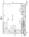
図7は、本発明の実施の形態2の液晶表示モジュールにおける、液晶表示パネル10の周囲にドレインドライバ130およびゲートドライバ140を配置した状態を示す図である。
本実施の形態の液晶表示モジュールでは、タイミングコントローラ110、ドレインドライバ130を構成する半導体チップICd、ゲートドライバ140を構成する半導体チップICgが、液晶表示パネル10のTFT基板側のガラス基板(SUB1)上に実装される。
そして、タイミングコントロール110から、ゲートドライバ140を構成する半導体チップICgに供給される信号、および電源回路120からゲートドライバ140を構成する半導体チップICgに供給される電源電圧は、液晶表示パネル10のTFT基板側のガラス基板(SUB1)上に形成された信号線を介して、ゲートドライバ140を構成する各半導体チップICgに供給される。
ここで、電源回路120は、液晶表示パネル10の外部に設置される。
【0026】
また、タイミングコントロール110から、ドレインドライバ130を構成する半導体チップICdに供給される信号、および電源回路120からドレインドライバ130を構成する半導体チップICdに供給される階調基準電圧は、液晶表示パネル10のTFT基板側のガラス基板(SUB1)上に形成された信号線を介して、各ドレインドライバ130を構成する半導体チップICdに供給される。
但し、ドレインドライバ130を構成する半導体チップ内部の論理回路用の電源電圧は、電源回路120→フレキシブルプリント基板150を介して、各ドレインドライバ130に供給される。
本実施の形態においても、液晶表示パネル10のTFT基板側のガラス基板(SUB1)上に形成される信号線の配線間隔を、前述したような配線間隔とすることにより、信号線を配置するスペースを大きくすることなく、保護膜に欠陥が生じても信号線の酸化、電食を防止することが可能となる。
【0027】
なお、本実施の形態において、ドレインドライバ130を構成する半導体チップ内の論理回路用の電源電圧を、液晶表示パネル10のTFT基板側のガラス基板(SUB1)上に形成した信号線を介して、各ドレインドライバ130に供給するようにしてもよい。
この場合にも、前述したような配線間隔とすることにより、信号線を配置するスペースを大きくすることなく、保護膜に欠陥が生じても信号線の酸化、電食を防止することが可能となる。
また、前記各実施の形態では、本発明を縦電界方式の液晶表示パネルに適用した場合について説明したが、これに限定されるものではなく、横電界方式の液晶表示パネルにも適用可能である。
また、前記各実施の形態では、本発明をTFT方式の液晶表示装置に適用した場合について説明したが、これに限定されるものではなく、本発明は、STN方式の単純マトリクス形液晶表示装置にも適用可能であることは言うまでもない。
以上、本発明者によってなされた発明を、前記発明の実施の形態に基づき具体的に説明したが、本発明は、前記発明の実施の形態に限定されるものではなく、その要旨を逸脱しない範囲において種々変更可能であることは勿論である。
【0028】
【発明の効果】
本願において開示される発明のうち代表的なものによって得られる効果を簡単に説明すれば、下記のとおりである。
本発明の液晶表示装置によれば、電源電圧、および信号を供給する信号線を、液晶表示素子の一方の基板上に配置する際に、信号線を配置するスペースを大きくすることなく、保護膜に欠陥が生じても信号線の酸化、電食を防止することが可能となる。
【図面の簡単な説明】
【図1】本発明の実施の形態1の液晶表示モジュールにおける、液晶表示パネルの周囲にドレインドライバおよびゲートドライバを配置した状態を示す図である。
【図2】図1中の点線の円の部分を拡大して示す図である。
【図3】本発明の実施の形態1における、信号線の配線間隔を説明するための図である。
【図4】本発明が適用されるTFT方式の液晶表示モジュールの概略構成を示すブロック図である。
【図5】図4に示す液晶表示パネルの一例の等価回路を示す図である。
【図6】図4に示す液晶表示パネルの他の例の等価回路を示す図である。
【図7】本発明の実施の形態2の液晶表示モジュールにおける、液晶表示パネルの周囲にドレインドライバおよびゲートドライバを配置した状態を示す図である。
【図8】従来の液晶表示モジュールにおける、液晶表示パネルの周囲にドレインドライバおよびゲートドライバを配置した状態を示す図である。
【符号の説明】
10…液晶表示パネル、20…タイミングコントロール基板、30…ドレイン基板、31,41…TCP、40…ゲート基板、50,51〜55,131、132,134,135,141,142…信号線、60,61…フレキシブルケーブル、100…インタフェース部、110…タイミングコントローラ、120…電源回路、121…正電圧生成回路、122…負電圧生成回路、123…コモン電極(対向電極)電圧生成回路、124…ゲート電極電圧生成回路、130…ドレインドライバ、133…表示データのバスライン、140…ゲートドライバ、150…フレキシブルプリント配線基板、AR…表示領域、ITO1…画素電極、ITO2…コモン電極、D…ドレイン信号線、G…ゲート信号線、TFT1,TFT2…薄膜トランジスタ、CLC…液晶容量、CADD…付加容量、CSTG…保持容量、CL…共通信号線、ICd,ICg…半導体チップ、SUB1,SUB2…ガラス基板。[0001]
BACKGROUND OF THE INVENTION
The present invention relates to a liquid crystal display device, and more particularly to a technique effective in arranging signal lines on a liquid crystal display panel.
[0002]
[Prior art]
STN ( S uper T wisted N ematic) method or TFT ( T hin F ilm T The liquid crystal display module of ransistor is widely used as a display device such as a notebook personal computer.
These liquid crystal display devices include a liquid crystal display panel, a drive circuit (drain driver and gate driver) for driving the liquid crystal display panel, a display control device (or timing controller), and a power supply circuit.
Such a liquid crystal display device is described in, for example, Japanese Patent Application No. 9-71328.
[0003]
[Problems to be solved by the invention]
In the liquid crystal display module described above, a power supply voltage and a signal (pulse voltage) are respectively applied from the drain driver and the gate driver, thereby selectively driving the pixels in the liquid crystal display panel and displaying an image.
At that time, generally, a flexible cable is used to connect the timing control board and the drain board, and the drain board and the gate board, and the power supply voltage and the signal output from the timing control board are respectively connected to the drain board, The pixel is supplied to the gate substrate to drive the pixels in the liquid crystal display panel.
However, when using a so-called flexible cable-less system that does not use a flexible cable as a system for supplying the power supply voltage and drive voltage output from the timing control board to the drain driver and gate driver, respectively, the timing control It is necessary to provide a signal line for transmitting a power supply voltage and a driving voltage output from the substrate on one glass substrate of the liquid crystal display panel.
[0004]
In the case described above, since the power supply voltage or the signal voltage value supplied to each signal line is different, an electric field proportional to the potential difference is generated between the signal lines.
When this electric field strength is strong, a problem arises in that the metal material constituting the signal line reacts with oxygen in the air and oxidizes and galvanizes.
In order to solve such problems, conventionally, (1) the signal lines are spaced to some extent, or (2) the signal lines are covered with a protective film so that they are not exposed to air. It was.
However, the above-mentioned method (1) has a drawback that the space for wiring the signal lines becomes large and cannot cope with the narrow frame of the liquid crystal display panel, and the above-mentioned method (2) has a drawback. The film has a low density, and if a defect occurs, the signal line is partially exposed to the atmosphere, so the potential difference between the signal lines is large, and if the gap is small, a strong electric field There is a drawback that electric corrosion occurs in the place where it is exposed to the atmosphere.
[0005]
The present invention has been made to solve the above-described problems of the prior art, and an object of the present invention is to arrange a plurality of signal lines on one substrate of a liquid crystal display element in a liquid crystal display device. An object of the present invention is to provide a technique capable of preventing oxidation and electrolytic corrosion of a signal line without increasing the space for arranging the signal line and even when a defect occurs in the protective film.
The above and other objects and novel features of the present invention will become apparent from the description of this specification and the accompanying drawings.
[0006]
[Means for Solving the Problems]
Of the inventions disclosed in this application, the outline of typical ones will be briefly described as follows.
That is, the present invention is a liquid crystal display device including a liquid crystal display element having a pair of substrates and a liquid crystal sandwiched between the pair of substrates, a plurality of drive circuits, a display control device, and a power supply circuit. The liquid crystal display element has a plurality of signals for supplying a power supply voltage from the power supply circuit and a signal from the display control device to the plurality of driving circuits on one of the pair of substrates. And at least a part of the plurality of signal lines has a non-uniform wiring interval between adjacent signal lines, and is between the adjacent signal lines determined from the voltage on each signal line. It is characterized by being variable according to the potential difference.
In a preferred embodiment of the present invention, at least a part of the plurality of signal lines has a larger wiring interval between the adjacent signal lines as the potential difference between the adjacent signal lines is larger. It is characterized by being wide.
[0007]
The present invention is a liquid crystal display device including a liquid crystal display element having a pair of substrates and a liquid crystal sandwiched between the pair of substrates, a plurality of drive circuits, a display control device, and a power supply circuit. The liquid crystal display element has a plurality of signals for supplying a power supply voltage from the power supply circuit and a signal from the display control device to the plurality of driving circuits on one of the pair of substrates. An electric field between adjacent signal lines, wherein a part of the plurality of signal lines has a wiring interval determined from a voltage on each signal line. It is characterized by being arranged at intervals at which the intensity is an electric field intensity at which no electrolytic corrosion occurs.
[0008]
The present invention is a liquid crystal display device including a liquid crystal display element having a pair of substrates and a liquid crystal sandwiched between the pair of substrates, a plurality of drive circuits, a display control device, and a power supply circuit. The liquid crystal display element has a plurality of signals for supplying a power supply voltage from the power supply circuit and a signal from the display control device to the plurality of driving circuits on one of the pair of substrates. An electric field between adjacent signal lines, wherein a part of the plurality of signal lines has a wiring interval determined from a voltage on each signal line. The electric field strength is an electric field strength at which the electric corrosion does not occur.
[0009]
In a preferred embodiment of the present invention, the part of the signal lines includes a signal line that supplies a liquid crystal driving reference voltage when driving the liquid crystal, and supplies the liquid crystal driving reference voltage. Is disposed at a position closest to the liquid crystal side, and the remaining signal lines among the some signal lines are signals for which the signal line having the highest voltage value on the signal line supplies the liquid crystal driving reference voltage. The potential difference between the adjacent signal lines determined from the voltage on each signal line is minimized with respect to the signal line having the highest voltage value on the signal line, which is arranged at the farthest position from the line. It is arranged so that it may be arranged.
In a preferred embodiment of the present invention, the part of the signal lines includes a signal line that is supplied from a display control device and that supplies a pulse voltage signal whose voltage level changes over time, The voltage on the signal line for supplying the pulse voltage signal is defined by the time average voltage value of the pulse voltage.
[0010]
According to the above means, when the power supply voltage and a signal line for supplying a signal are arranged on one substrate of the liquid crystal display element to each drive circuit (drain driver or gate driver) from the display control device, The distance between the signal lines is determined so that the electric field strength between adjacent signal lines determined by the voltage on each signal line is an electric field intensity at which no electric corrosion occurs, that is, the voltage on each signal line. When the potential difference between adjacent signal lines is large, the interval between the signal lines is increased, and when the potential difference between adjacent signal lines determined by the voltage on each signal line is small Since the interval between the signal lines is reduced, it is possible to prevent the signal lines from being oxidized and eroded even if a defect occurs in the protective film without increasing the space for arranging the signal lines.
[0011]
DETAILED DESCRIPTION OF THE INVENTION
Hereinafter, embodiments of the present invention will be described in detail with reference to the drawings.
Note that components having the same function are denoted by the same reference symbols throughout the drawings for describing the embodiment, and the repetitive description thereof will be omitted.
[Embodiment 1]
[Basic configuration of TFT liquid crystal display module to which the present invention is applied]
FIG. 4 is a block diagram showing a schematic configuration of a TFT liquid crystal display module to which the present invention is applied.
In the liquid crystal display module (LCM) of the present embodiment, a drain driver 130 is disposed on one side of the long side of the liquid crystal display panel (TFT-LCD) 10, and on one side of the short side of the liquid
The liquid
[0012]
FIG. 5 is a diagram showing an equivalent circuit of an example of the liquid
As shown in the figure, the liquid
Each pixel includes two adjacent signal lines (drain signal line (D) or gate signal line (G)) and two adjacent signal lines (gate signal line (G) or drain signal line (D)). It is arranged in the intersection area.
Each pixel has a thin film transistor (TFT1, TFT2), the source electrode of the thin film transistor (TFT1, TFT2) of each pixel is connected to the pixel electrode (ITO1), and the pixel electrode (ITO1) and the common electrode (or counter electrode) Since the liquid crystal layer is provided between (ITO2) and the pixel electrode (ITO1) and the common electrode (ITO2), the liquid crystal capacitance (CLC) is equivalently connected.
Further, an additional capacitor (CADD) is connected between the pixel electrode (ITO1) and the previous gate signal line (G).
[0013]
FIG. 6 is a diagram showing an equivalent circuit of another example of the liquid
In the example shown in FIG. 5, an additional capacitor (CADD) is formed between the previous gate signal line (G) and the source electrode. In the equivalent circuit of the example shown in FIG. 6, the common electrode (ITO2) is connected to the common electrode (ITO2). The difference is that a storage capacitor (CSTG) is formed between the common signal line (CL) to which the supplied Vcom voltage is applied and the pixel electrode (ITO1).
In FIGS. 5 and 6, AR is a display area.
Although the present invention can be applied to both, in the former method, the gate signal line (G) pulse in the former stage jumps into the pixel electrode via the additional capacitor (CADD), whereas in the latter method, the jump in Therefore, better display is possible.
5 and 6 show an equivalent circuit of a vertical electric field type liquid crystal display panel. Further, FIGS. 5 and 6 are circuit diagrams, which are drawn corresponding to an actual geometric arrangement. ing.
[0014]
In the liquid
In addition, the gate electrodes of the thin film transistors (TFT1, TFT2) in each pixel arranged in the row direction are connected to the gate signal line (G), respectively, and each gate signal line (G) has one horizontal scanning time in the row direction. It is connected to a gate driver 140 that supplies a scanning drive voltage (positive bias voltage or negative bias voltage) to the gate electrode of the thin film transistor (TFT1, TFT2) of each pixel.
[0015]
The
The
When the display timing signal is input, the
At that time, the
The display data from the main body computer is, for example, 6 bits or 8 bits, and is in units of one pixel, ie, each unit of red (R), green (G), and blue (B) data as a set. Forwarded to
[0016]
The
In addition, when the first display timing signal is input after the vertical synchronization signal is input, the
Furthermore, the
As a result, a plurality of thin film transistors (TFT1, TFT2) connected to each gate signal line (G) of the liquid
With the above operation, an image is displayed on the liquid
[0017]
The
The positive
The positive polarity reference voltage (for example, V ″ 0 to V ″ 4) and the negative polarity reference voltage (for example, V ″ 5 to V ″ 9) are supplied to each drain driver 130.
Each drain driver 130 is also supplied with an AC signal (AC timing signal; M) from the
The common electrode voltage generation circuit 123 is a drive voltage to be applied to the common electrode (ITO2), and the gate electrode voltage generation circuit 124 is a drive voltage to be applied to the gate electrodes of the thin film transistors (TFT1 and TFT2) (positive bias voltage and negative bias voltage). ) Is generated.
[0018]
[Configuration of Liquid Crystal Display Module of
FIG. 1 is a diagram showing a state in which a drain driver 130 and a gate driver 140 are arranged around a liquid
In FIG. 1, 31 is a drain side TCP (Tape Carrier Package) mounted between one glass substrate (TFT substrate side glass substrate) of the liquid
A semiconductor chip (ICd) constituting the drain driver 130 is mounted on the drain side TCP (31), and a semiconductor chip (ICg) constituting the gate driver 140 is mounted on the gate side TCP (41).
A
[0019]
[Configuration of conventional LCD module]
FIG. 8 is a diagram showing a state in which the drain driver 130 and the gate driver 140 are arranged around the liquid
As shown in FIG. 8, in the conventional liquid crystal display module, the power supply voltage and signal output from the
The power supply voltage and signal output from the
[0020]
[Features of the liquid crystal display module of the embodiment of the present invention]
FIG. 2 is an enlarged view showing a dotted circle in FIG.
In FIG. 2, SUB1 is a glass substrate on the TFT substrate side, and SUB2 is a glass substrate on the filter substrate side.
In the present embodiment, the power supply voltage and signal sent from the
Here, there are five types of power supply voltages sent from the
These signal lines 50 are made of Al (aluminum), Cr (chromium), molybdenum (Mo), or the like, and are usually covered with a protective film or the like so as not to come into contact with the atmosphere.
In FIG. 2, nine signal lines are shown, but one is a dummy signal line.
Next, the wiring interval between the signal lines, which is a feature of this embodiment, will be described with reference to FIG.
In FIG. 3, the power supply voltages (Vcom, VGH, VGL, Vcc, GND) will be mainly described.
Table 1 shows the voltage values of these power supply voltages.
[0021]
◎
[Table 1]
Vcom is a voltage applied to the common electrode (ITO2), VGH is a voltage for turning on the thin film transistors (TFT1, TFT2), VGL is a voltage for turning off the thin film transistors (TFT1, TFT2), and Vcc is a gate driver. The power supply voltage GND (or Vss) for the logic circuit inside the semiconductor chip 140 is a ground voltage.
As shown in FIG. 3, the voltage Vcom is a voltage applied to the common electrode (ITO 2) and needs to be supplied to the inside of the
As shown in Table 1, the other signal lines (52 to 55) are arranged so that the potential difference between the adjacent signal lines is minimized.
In this embodiment, as shown in FIG. 3, a signal line 51 supplying Vcom → a signal line 52 supplying VGL → a
[0023]
In this embodiment, the interval between the signal lines having the largest potential difference between the adjacent signal lines (in this embodiment, the interval between the
In this embodiment, as shown in Table 1, the distance between the
Therefore, the electric field strength is 16.7 (= 16.7 / 1.0) (V / mm).
Then, the wiring interval between the remaining signal lines is determined so as to be substantially equal to the electric field strength described above.
Therefore, in this embodiment, as shown in Table 1, the wiring interval between the
[0024]
Thus, by determining the wiring interval of the signal lines (51 to 55), no electric corrosion occurs, and it is possible to arrange the wiring in the smallest space compared to other arrangements.
In the above description, the case where the electric field strength at which no electric corrosion occurs is 16.7 (V / mm) has been described. However, the electric field strength at which no electric corrosion occurs depends on the signal line material and the protective film. Since it differs for each liquid crystal display panel depending on the capacity and the like, it is necessary to set an optimum electric field strength as an electric field strength that does not cause electrolytic corrosion for each liquid crystal display panel. In the above description, the wiring interval of the signal lines for supplying the power supply voltages (Vcom, VGH, VGL, Vcc, GND) has been described. However, the signal (clock (CL3), FLM (frame start instruction signal), OE ( The wiring interval with the signal line supplying the output enable signal)) can be determined in the same manner.
However, since these signals are voltages whose voltage values change with time (so-called pulse voltage), the voltage values in this case need to be defined by taking a time average.
[0025]
[Embodiment 2]
[Configuration of Liquid Crystal Display Module of Embodiment of the Present Invention]
FIG. 7 is a diagram showing a state in which the drain driver 130 and the gate driver 140 are arranged around the liquid
In the liquid crystal display module of the present embodiment, the
The signal supplied from the
Here, the
[0026]
The signal supplied from the
However, the power supply voltage for the logic circuit inside the semiconductor chip constituting the drain driver 130 is supplied to each drain driver 130 via the
Also in the present embodiment, a space for arranging signal lines is obtained by setting the wiring intervals of the signal lines formed on the glass substrate (SUB1) on the TFT substrate side of the liquid
[0027]
In the present embodiment, the power supply voltage for the logic circuit in the semiconductor chip constituting the drain driver 130 is supplied via the signal line formed on the glass substrate (SUB1) on the TFT substrate side of the liquid
Also in this case, by using the wiring interval as described above, it is possible to prevent the signal line from being oxidized and eroded even if a defect occurs in the protective film without increasing the space for arranging the signal line. Become.
In each of the above-described embodiments, the case where the present invention is applied to a vertical electric field type liquid crystal display panel has been described. However, the present invention is not limited to this, and can be applied to a horizontal electric field type liquid crystal display panel. .
In each of the above embodiments, the present invention is applied to a TFT liquid crystal display device. However, the present invention is not limited to this, and the present invention is applied to an STN simple matrix liquid crystal display device. It goes without saying that is also applicable.
The invention made by the present inventor has been specifically described based on the embodiment of the invention, but the invention is not limited to the embodiment of the invention and does not depart from the gist of the invention. Of course, various changes can be made.
[0028]
【The invention's effect】
The effects obtained by the representative ones of the inventions disclosed in the present application will be briefly described as follows.
According to the liquid crystal display device of the present invention, when the signal line for supplying the power supply voltage and the signal is arranged on one substrate of the liquid crystal display element, the protective film is formed without increasing the space for arranging the signal line. Even if a defect occurs, it is possible to prevent the signal line from being oxidized and electrolytic corrosion.
[Brief description of the drawings]
FIG. 1 is a diagram showing a state in which a drain driver and a gate driver are arranged around a liquid crystal display panel in a liquid crystal display module according to
2 is an enlarged view showing a dotted circle in FIG. 1. FIG.
FIG. 3 is a diagram for explaining signal line wiring intervals in the first embodiment of the present invention;
FIG. 4 is a block diagram showing a schematic configuration of a TFT liquid crystal display module to which the present invention is applied.
5 is a diagram showing an equivalent circuit of an example of the liquid crystal display panel shown in FIG. 4. FIG.
6 is a diagram showing an equivalent circuit of another example of the liquid crystal display panel shown in FIG.
7 is a diagram showing a state in which a drain driver and a gate driver are arranged around a liquid crystal display panel in a liquid crystal display module according to a second embodiment of the present invention. FIG.
FIG. 8 is a diagram showing a state in which a drain driver and a gate driver are arranged around a liquid crystal display panel in a conventional liquid crystal display module.
[Explanation of symbols]
DESCRIPTION OF
Claims (16)
前記一対の基板の一方の基板上には、複数のゲート信号線と該複数のゲート信号線に交差するように配置された複数のドレイン信号線が配置されて表示領域を形成しており、
前記一方の基板の一辺側には、テープ上に搭載され、前記複数のドレイン信号線に電気的に接続されているドレインドライバが配置されており、さらに該ドレインドライバが配置されたテープは、前記一方の基板の一辺に沿って複数個並んで配置されており、
前記複数個の該ドレインドライバが配置されたテープは、前記液晶表示素子が配置されている側とは反対側において、ドレイン基板により共通に接続されており、
前記一方の基板の前記一辺と隣接する別の一辺側の角部には、テープ上に搭載され、前記複数のゲート信号線に電気的に接続されたゲートドライバが配置されており、
前記一方の基板上には、前記複数のドレインドライバが搭載されたテープのうち、前記一方の基板の別の一辺側に最も近い位置に配置されたドレインドライバが搭載されたテープから、前記ゲートドライバが搭載されたテープに接続された複数の信号配線が配置されており、
前記複数の信号配線は、前記ドレイン基板に接続され、タイミングコントローラ及び電源回路を搭載したタイミングコントロール基板からの信号を伝達する信号配線であり、
前記一対の基板に配置されたコモン電極に印加する電圧を供給する信号配線と、
前記ドレイン信号線と前記ゲート信号線の交点に対応して配置されている薄膜トランジスタをオンする電圧を供給する信号配線と、
前記薄膜トランジスタをオフする電圧を供給する信号配線と、
前記ゲートドライバの電源電圧を供給する信号配線と、
接地電圧を供給する信号配線とを有し、
前記複数の信号配線は、配線間隔が第一の配線間隔を有する隣接する一組の信号配線と、前記第一の配線間隔よりも狭い第二の配線間隔を有する隣接する他の一組の信号配線を有しており、
前記第一の配線間隔を有する隣接する前記一組の信号配線間の電位差が、前記第二の配線間隔を有する隣接する前記他の一組の信号配線間の電位差よりも大きく、
前記コモン電極に印加する電圧(Vcom)、
前記薄膜トランジスタをオンする電圧(VGH)、
前記薄膜トランジスタをオフする電圧(VGL)、
前記ゲートドライバの電源電圧(Vcc)、
接地電圧(GND)は、
VGH>Vcom>Vcc>GND>VGL、
の関係を満たすことを特徴とする液晶表示装置。 A liquid crystal display device having a liquid crystal display element having a pair of substrates and a liquid crystal sandwiched between the pair of substrates,
On one substrate of the pair of substrates, a plurality of gate signal lines and a plurality of drain signal lines arranged to cross the plurality of gate signal lines are arranged to form a display region,
A drain driver mounted on a tape and electrically connected to the plurality of drain signal lines is disposed on one side of the one substrate, and the tape on which the drain driver is disposed is It is arranged side by side along one side of one substrate,
The tape on which the plurality of drain drivers are arranged is connected in common by a drain substrate on the side opposite to the side on which the liquid crystal display element is arranged,
A gate driver mounted on a tape and electrically connected to the plurality of gate signal lines is disposed at a corner on another side adjacent to the one side of the one substrate,
On the one substrate, among the tapes on which the plurality of drain drivers are mounted, the gate driver from the tape on which the drain driver disposed at a position closest to another side of the one substrate is mounted. A plurality of signal wires connected to the tape on which the
The plurality of signal wirings are signal wirings that are connected to the drain substrate and transmit signals from a timing control board on which a timing controller and a power supply circuit are mounted,
A signal wiring for supplying a voltage to be applied to the common electrode disposed on the pair of substrates;
A signal wiring for supplying a voltage for turning on the thin film transistor disposed corresponding to the intersection of the drain signal line and the gate signal line;
A signal wiring for supplying a voltage for turning off the thin film transistor;
A signal wiring for supplying a power supply voltage of the gate driver;
Signal wiring for supplying ground voltage,
The plurality of signal wirings include a pair of adjacent signal wirings having a first wiring spacing and a pair of adjacent signals having a second wiring spacing narrower than the first wiring spacing. Have wiring,
The potential difference between the set of adjacent signal wires having the first wiring interval is larger than the potential difference between the other set of adjacent signal wires having the second wire interval,
Voltage (Vcom) applied to the common electrode,
A voltage (VGH) for turning on the thin film transistor;
A voltage (VGL) for turning off the thin film transistor;
Power supply voltage (Vcc) of the gate driver,
The ground voltage (GND) is
VGH>Vcom>Vcc>GND> VGL,
Liquid crystal display device you and satisfies the relationship.
前記ゲートドライバの電源電圧を供給する信号配線と、前記接地電圧を供給する信号配線とは隣接されており、
前記薄膜トランジスタをオンする電圧を供給する信号配線と前記ゲートドライバの電源電圧を供給する信号配線の配線間隔が、前記ゲートドライバの電源電圧を供給する信号配線と前記接地電圧を供給する信号配線の配線間隔よりも広いことを特徴とする請求項1または請求項2に記載の液晶表示装置。The signal wiring for supplying the voltage for turning on the thin film transistor and the signal wiring for supplying the power voltage of the gate driver are adjacent to each other.
The signal wiring for supplying the power voltage of the gate driver and the signal wiring for supplying the ground voltage are adjacent to each other.
The wiring interval between the signal wiring for supplying the voltage for turning on the thin film transistor and the signal wiring for supplying the power supply voltage of the gate driver is such that the wiring of the signal wiring for supplying the power supply voltage of the gate driver and the signal wiring for supplying the ground voltage The liquid crystal display device according to claim 1 , wherein the liquid crystal display device is wider than the interval.
前記薄膜トランジスタをオンする電圧を供給する信号配線と前記ゲートドライバの電源電圧を供給する信号配線の配線間隔が、前記接地電圧を供給する信号配線と前記薄膜トランジスタをオフする電圧を供給する信号配線の配線間隔よりも広いことを特徴とする請求項4に記載の液晶表示装置。The signal wiring for supplying the voltage for turning on the thin film transistor and the signal wiring for supplying the power voltage of the gate driver are adjacent to each other.
The wiring interval between the signal wiring for supplying the voltage for turning on the thin film transistor and the signal wiring for supplying the power supply voltage of the gate driver is the wiring of the signal wiring for supplying the ground voltage and the signal wiring for supplying the voltage for turning off the thin film transistor. The liquid crystal display device according to claim 4 , wherein the liquid crystal display device is wider than the interval.
前記コモン電極に印加する電圧を供給する信号配線と、前記薄膜トランジスタをオフする電圧を供給する信号配線とは隣接されており、
前記薄膜トランジスタをオンする電圧を供給する信号配線と前記ゲートドライバの電源電圧を供給する信号配線の配線間隔が、前記コモン電極に印加する電圧を供給する信号配線と、前記薄膜トランジスタをオフする電圧を供給する信号配線の配線間隔よりも広いことを特徴とする請求項1または請求項2に記載の液晶表示装置。The signal wiring for supplying the voltage for turning on the thin film transistor and the signal wiring for supplying the power voltage of the gate driver are adjacent to each other.
The signal wiring for supplying a voltage to be applied to the common electrode and the signal wiring for supplying a voltage for turning off the thin film transistor are adjacent to each other.
A wiring interval between a signal wiring for supplying a voltage for turning on the thin film transistor and a signal wiring for supplying a power supply voltage for the gate driver is supplied with a signal wiring for supplying a voltage to be applied to the common electrode and a voltage for turning off the thin film transistor. The liquid crystal display device according to claim 1 , wherein the liquid crystal display device is wider than a wiring interval of the signal wiring.
前記薄膜トランジスタをオフする電圧を供給する信号配線と、前記接地電圧を供給する信号配線とは隣接されており、
前記コモン電極に印加する電圧を供給する信号配線と、前記薄膜トランジスタをオフする電圧を供給する信号配線の配線間隔が、前記薄膜トランジスタをオフする電圧を供給する信号配線と前記接地電圧を供給する信号配線の配線間隔よりも広いことを特徴とする請求項1または請求項2に記載の液晶表示装置。The signal wiring for supplying a voltage to be applied to the common electrode and the signal wiring for supplying a voltage for turning off the thin film transistor are adjacent to each other.
The signal wiring for supplying a voltage for turning off the thin film transistor and the signal wiring for supplying the ground voltage are adjacent to each other,
A signal wiring for supplying a voltage to be applied to the common electrode, and a signal wiring for supplying a voltage for turning off the thin film transistor, and a signal wiring for supplying the ground voltage. The liquid crystal display device according to claim 1 , wherein the liquid crystal display device is wider than the wiring interval.
前記接地電圧を供給する信号配線と、前記ゲートドライバの電源電圧を供給する信号配線は隣接されており、
前記コモン電極に印加する電圧を供給する信号配線と、前記薄膜トランジスタをオフする電圧を供給する信号配線の配線間隔が、前記接地電圧を供給する信号配線と前記ゲートドライバの電源電圧を供給する信号配線の配線間隔よりも広いことを特徴とする請求項1または請求項2に記載の液晶表示装置。The signal wiring for supplying a voltage to be applied to the common electrode and the signal wiring for supplying a voltage for turning off the thin film transistor are adjacent to each other.
The signal wiring for supplying the ground voltage and the signal wiring for supplying the power supply voltage of the gate driver are adjacent to each other.
A signal wiring for supplying a voltage to be applied to the common electrode, and a signal wiring for supplying a voltage for turning off the thin film transistor. A signal wiring for supplying the ground voltage and a signal wiring for supplying a power supply voltage for the gate driver. The liquid crystal display device according to claim 1 , wherein the liquid crystal display device is wider than the wiring interval.
前記接地電圧を供給する信号配線と、前記ゲートドライバの電源電圧を供給する信号配線は隣接されており、
前記接地電圧を供給する信号配線と前記薄膜トランジスタをオフする電圧を供給する信号配線の配線間隔が、前記接地電圧を供給する信号配線と、前記ゲートドライバの電源電圧を供給する信号配線の配線間隔よりも広いことを特徴とする請求項1または請求項2に記載の液晶表示装置。The signal wiring for supplying the ground voltage and the signal wiring for supplying a voltage for turning off the thin film transistor are adjacent to each other.
The signal wiring for supplying the ground voltage and the signal wiring for supplying the power supply voltage of the gate driver are adjacent to each other.
The wiring interval between the signal wiring for supplying the ground voltage and the signal wiring for supplying the voltage for turning off the thin film transistor is determined by the wiring interval between the signal wiring for supplying the ground voltage and the signal wiring for supplying the power supply voltage of the gate driver. The liquid crystal display device according to claim 1 , wherein the liquid crystal display device is wide.
前記一対のガラス基板の一方のガラス基板上には、複数のゲート信号線と該複数のゲート信号線に交差するように配置された複数のドレイン信号線が配置されて表示領域を形成しており、
前記一方のガラス基板の一辺側には、テープ上に搭載され、前記複数のドレイン信号線に電気的に接続されているドレインドライバが配置されており、さらに該ドレインドライバが配置されたテープは、前記一方の基板の一辺に沿って複数個並んで配置されており、
前記複数個の前記ドレインドライバが配置されたテープは、前記液晶表示素子が配置されている側とは反対側において、ドレイン基板により共通に接続されており、
前記一方のガラス基板の前記一辺と隣接する別の一辺側には、テープ上に搭載され、前記複数のゲート信号線に電気的に接続されたゲートドライバが配置されており、さらに該ゲートドライバが配置されたテープは、該別の一辺に沿って複数個並んで配置されており、
前記一方のガラス基板上には、前記複数のドレインドライバが搭載されたテープのうち、前記別の一辺側に最も近い位置に配置された前記ドレインドライバが搭載されたテープから、前記複数のゲートドライバが搭載されたテープのうち、前記一辺側に最も近い位置に配置された前記ゲートドライバが搭載されたテープに接続された複数の信号配線が配置されており、
前記複数の信号配線は、
前記一対のガラス基板に配置されたコモン電極に印加する電圧を供給する信号配線と、
前記ドレイン信号線と前記ゲート信号線の交点に対応して配置されている薄膜トランジスタをオンする電圧を供給する信号配線と、
前記薄膜トランジスタをオフする電圧を供給する信号配線と、
前記ゲートドライバの電源電圧を供給する信号配線と、
接地電圧を供給する信号配線とを有し、
前記コモン電極に印加する電圧を供給する信号配線と、前記薄膜トランジスタをオフする電圧を供給する信号配線とは隣接されており、
前記ゲートドライバの電源電圧を供給する信号配線と、前記接地電圧を供給する信号配線とは隣接されており、
前記コモン電極に印加する電圧を供給する信号配線と、前記薄膜トランジスタをオフする電圧を供給する信号配線の配線間隔が、前記ゲートドライバの電源電圧を供給する信号配線と前記接地電圧を供給する信号配線の配線間隔よりも広く、
前記コモン電極に印加する電圧を供給する信号配線と、前記薄膜トランジスタをオフする電圧を供給する信号配線間の電位差が、前記ゲートドライバの電源電圧を供給する信号配線と前記接地電圧を供給する信号配線間の電位差よりも大きいことを特徴とする液晶表示装置。A liquid crystal display device having a liquid crystal display element having a pair of glass substrates and a liquid crystal sandwiched between the pair of glass substrates,
On one glass substrate of the pair of glass substrates, a plurality of gate signal lines and a plurality of drain signal lines arranged to cross the plurality of gate signal lines are arranged to form a display region. ,
A drain driver mounted on a tape and electrically connected to the plurality of drain signal lines is disposed on one side of the one glass substrate, and the tape on which the drain driver is disposed is A plurality are arranged along one side of the one substrate,
The tape on which the plurality of drain drivers are arranged is connected in common by a drain substrate on the side opposite to the side on which the liquid crystal display element is arranged,
A gate driver mounted on a tape and electrically connected to the plurality of gate signal lines is disposed on another side adjacent to the one side of the one glass substrate. The arranged tapes are arranged side by side along the other side,
On the one glass substrate, among the tapes on which the plurality of drain drivers are mounted, the plurality of gate drivers from the tape on which the drain driver disposed at a position closest to the other side is mounted. A plurality of signal wirings connected to the tape on which the gate driver arranged at a position closest to the one side is mounted,
The plurality of signal wirings are:
A signal wiring for supplying a voltage to be applied to the common electrode disposed on the pair of glass substrates;
A signal wiring for supplying a voltage for turning on the thin film transistor disposed corresponding to the intersection of the drain signal line and the gate signal line;
A signal wiring for supplying a voltage for turning off the thin film transistor;
A signal wiring for supplying a power supply voltage of the gate driver;
Signal wiring for supplying ground voltage,
The signal wiring for supplying a voltage to be applied to the common electrode and the signal wiring for supplying a voltage for turning off the thin film transistor are adjacent to each other.
The signal wiring for supplying the power voltage of the gate driver and the signal wiring for supplying the ground voltage are adjacent to each other.
A signal wiring for supplying a voltage to be applied to the common electrode, and a signal wiring for supplying a voltage for turning off the thin film transistor, a signal wiring for supplying a power supply voltage for the gate driver and a signal wiring for supplying the ground voltage. Wider than the wiring spacing of
A potential difference between a signal wiring for supplying a voltage to be applied to the common electrode and a signal wiring for supplying a voltage for turning off the thin film transistor is a signal wiring for supplying a power supply voltage for the gate driver and a signal wiring for supplying the ground voltage. A liquid crystal display device characterized by being larger than a potential difference therebetween.
前記ドレイン基板に接続され、タイミングコントローラ及び電源回路を搭載したタイミングコントロール基板からの信号を伝達する信号配線である請求項10に記載の液晶表示装置。The plurality of signal wirings are:
The liquid crystal display device according to claim 10 , wherein the liquid crystal display device is a signal line connected to the drain substrate and transmitting a signal from a timing control substrate on which a timing controller and a power supply circuit are mounted.
前記薄膜トランジスタをオンする電圧(VGH)、
前記薄膜トランジスタをオフする電圧(VGL)、
前記ゲートドライバの電源電圧(Vcc)、
接地電圧(GND)は、
VGH>Vcom>Vcc>GND>VGL、
の関係を満たすことを特徴とする請求項10または請求項11に記載の液晶表示装置。Voltage (Vcom) applied to the common electrode,
A voltage (VGH) for turning on the thin film transistor;
A voltage (VGL) for turning off the thin film transistor;
Power supply voltage (Vcc) of the gate driver,
The ground voltage (GND) is
VGH>Vcom>Vcc>GND> VGL,
The liquid crystal display device according to claim 10 , wherein the relationship is satisfied.
Priority Applications (1)
| Application Number | Priority Date | Filing Date | Title |
|---|---|---|---|
| JP2000332023A JP4283431B2 (en) | 2000-10-31 | 2000-10-31 | Liquid crystal display |
Applications Claiming Priority (1)
| Application Number | Priority Date | Filing Date | Title |
|---|---|---|---|
| JP2000332023A JP4283431B2 (en) | 2000-10-31 | 2000-10-31 | Liquid crystal display |
Related Child Applications (1)
| Application Number | Title | Priority Date | Filing Date |
|---|---|---|---|
| JP2005307919A Division JP4294631B2 (en) | 2005-10-24 | 2005-10-24 | Liquid crystal display |
Publications (3)
| Publication Number | Publication Date |
|---|---|
| JP2002140042A JP2002140042A (en) | 2002-05-17 |
| JP2002140042A5 JP2002140042A5 (en) | 2008-02-14 |
| JP4283431B2 true JP4283431B2 (en) | 2009-06-24 |
Family
ID=18808282
Family Applications (1)
| Application Number | Title | Priority Date | Filing Date |
|---|---|---|---|
| JP2000332023A Expired - Fee Related JP4283431B2 (en) | 2000-10-31 | 2000-10-31 | Liquid crystal display |
Country Status (1)
| Country | Link |
|---|---|
| JP (1) | JP4283431B2 (en) |
Families Citing this family (8)
| Publication number | Priority date | Publication date | Assignee | Title |
|---|---|---|---|---|
| KR100864501B1 (en) * | 2002-11-19 | 2008-10-20 | 삼성전자주식회사 | Liquid crystal display |
| TWI238444B (en) * | 2002-12-10 | 2005-08-21 | Seiko Epson Corp | Method for manufacturing optoelectronic device, optoelectronic device and electronic machine |
| JP2006098495A (en) * | 2004-09-28 | 2006-04-13 | Kyocera Corp | Display device |
| JP4535845B2 (en) | 2004-10-29 | 2010-09-01 | 富士通セミコンダクター株式会社 | Semiconductor device |
| JP4650343B2 (en) * | 2005-07-15 | 2011-03-16 | セイコーエプソン株式会社 | Electro-optical device and electronic apparatus |
| JP2008014996A (en) * | 2006-07-03 | 2008-01-24 | Seiko Epson Corp | Electrooptical device and electronic equipment |
| US7700700B2 (en) * | 2007-01-26 | 2010-04-20 | Arkema Inc. | Vinylidene fluoride copolymer composition with improved low-temperature impact properties |
| KR102569727B1 (en) * | 2017-11-08 | 2023-08-22 | 엘지디스플레이 주식회사 | Display device |
-
2000
- 2000-10-31 JP JP2000332023A patent/JP4283431B2/en not_active Expired - Fee Related
Also Published As
| Publication number | Publication date |
|---|---|
| JP2002140042A (en) | 2002-05-17 |
Similar Documents
| Publication | Publication Date | Title |
|---|---|---|
| JP4673801B2 (en) | Liquid crystal display device and manufacturing method thereof | |
| JP4550334B2 (en) | Liquid crystal display device and method of manufacturing liquid crystal display device | |
| US20080048963A1 (en) | Display method for improving image quality and device used the same | |
| JPH11133926A (en) | Semi-conductor integrated circuit device and liquid crystal display device | |
| US7463324B2 (en) | Liquid crystal display panel of line on glass type | |
| US8085231B2 (en) | Display device | |
| KR101048700B1 (en) | LCD and its driving method | |
| JP4283431B2 (en) | Liquid crystal display | |
| JP5022651B2 (en) | Display device | |
| KR20030054897A (en) | Liquid crystal display | |
| JP4294631B2 (en) | Liquid crystal display | |
| JP3660838B2 (en) | Liquid crystal display | |
| JP4170309B2 (en) | Liquid crystal display | |
| JP4516307B2 (en) | Liquid crystal display | |
| JP4562963B2 (en) | Liquid crystal display | |
| JP2002055323A (en) | Liquid crystal display device | |
| KR100555302B1 (en) | Liquid crystal display device unified control signal generater and driving circuit | |
| US7663727B2 (en) | Display device | |
| KR101007687B1 (en) | Liquid crystal display device | |
| JPH11352937A (en) | Liquid crystal display device | |
| JP2004093821A (en) | Liquid crystal display | |
| JP2002350810A (en) | Liquid crystal display device and driving method therefor, and image display application equipment | |
| JP2003223152A (en) | Active matrix liquid crystal display device and picture display device using the same | |
| KR100899628B1 (en) | Tft-lcd panel with gate high level voltage and gate low level voltage lines | |
| KR100912697B1 (en) | Liquid crystal display |
Legal Events
| Date | Code | Title | Description |
|---|---|---|---|
| A521 | Written amendment |
Free format text: JAPANESE INTERMEDIATE CODE: A523 Effective date: 20051024 |
|
| A621 | Written request for application examination |
Free format text: JAPANESE INTERMEDIATE CODE: A621 Effective date: 20051024 |
|
| A521 | Written amendment |
Free format text: JAPANESE INTERMEDIATE CODE: A523 Effective date: 20071026 |
|
| A871 | Explanation of circumstances concerning accelerated examination |
Free format text: JAPANESE INTERMEDIATE CODE: A871 Effective date: 20071026 |
|
| A975 | Report on accelerated examination |
Free format text: JAPANESE INTERMEDIATE CODE: A971005 Effective date: 20071116 |
|
| RD13 | Notification of appointment of power of sub attorney |
Free format text: JAPANESE INTERMEDIATE CODE: A7433 Effective date: 20071130 |
|
| A521 | Written amendment |
Free format text: JAPANESE INTERMEDIATE CODE: A523 Effective date: 20071221 |
|
| A521 | Written amendment |
Free format text: JAPANESE INTERMEDIATE CODE: A523 Effective date: 20071214 |
|
| A131 | Notification of reasons for refusal |
Free format text: JAPANESE INTERMEDIATE CODE: A131 Effective date: 20080205 |
|
| A521 | Written amendment |
Free format text: JAPANESE INTERMEDIATE CODE: A523 Effective date: 20080407 |
|
| A131 | Notification of reasons for refusal |
Free format text: JAPANESE INTERMEDIATE CODE: A131 Effective date: 20080520 |
|
| A521 | Written amendment |
Free format text: JAPANESE INTERMEDIATE CODE: A523 Effective date: 20080722 |
|
| A521 | Written amendment |
Free format text: JAPANESE INTERMEDIATE CODE: A523 Effective date: 20080822 |
|
| A02 | Decision of refusal |
Free format text: JAPANESE INTERMEDIATE CODE: A02 Effective date: 20081111 |
|
| A521 | Written amendment |
Free format text: JAPANESE INTERMEDIATE CODE: A523 Effective date: 20081211 |
|
| A521 | Written amendment |
Free format text: JAPANESE INTERMEDIATE CODE: A523 Effective date: 20081212 |
|
| A521 | Written amendment |
Free format text: JAPANESE INTERMEDIATE CODE: A523 Effective date: 20090123 |
|
| A911 | Transfer of reconsideration by examiner before appeal (zenchi) |
Free format text: JAPANESE INTERMEDIATE CODE: A911 Effective date: 20090223 |
|
| TRDD | Decision of grant or rejection written | ||
| A01 | Written decision to grant a patent or to grant a registration (utility model) |
Free format text: JAPANESE INTERMEDIATE CODE: A01 Effective date: 20090317 |
|
| A01 | Written decision to grant a patent or to grant a registration (utility model) |
Free format text: JAPANESE INTERMEDIATE CODE: A01 |
|
| A61 | First payment of annual fees (during grant procedure) |
Free format text: JAPANESE INTERMEDIATE CODE: A61 Effective date: 20090319 |
|
| R150 | Certificate of patent or registration of utility model |
Free format text: JAPANESE INTERMEDIATE CODE: R150 |
|
| FPAY | Renewal fee payment (event date is renewal date of database) |
Free format text: PAYMENT UNTIL: 20120327 Year of fee payment: 3 |
|
| FPAY | Renewal fee payment (event date is renewal date of database) |
Free format text: PAYMENT UNTIL: 20120327 Year of fee payment: 3 |
|
| S531 | Written request for registration of change of domicile |
Free format text: JAPANESE INTERMEDIATE CODE: R313531 |
|
| FPAY | Renewal fee payment (event date is renewal date of database) |
Free format text: PAYMENT UNTIL: 20120327 Year of fee payment: 3 |
|
| R371 | Transfer withdrawn |
Free format text: JAPANESE INTERMEDIATE CODE: R371 |
|
| FPAY | Renewal fee payment (event date is renewal date of database) |
Free format text: PAYMENT UNTIL: 20120327 Year of fee payment: 3 |
|
| S111 | Request for change of ownership or part of ownership |
Free format text: JAPANESE INTERMEDIATE CODE: R313111 |
|
| S631 | Written request for registration of reclamation of domicile |
Free format text: JAPANESE INTERMEDIATE CODE: R313631 |
|
| FPAY | Renewal fee payment (event date is renewal date of database) |
Free format text: PAYMENT UNTIL: 20120327 Year of fee payment: 3 |
|
| R350 | Written notification of registration of transfer |
Free format text: JAPANESE INTERMEDIATE CODE: R350 |
|
| FPAY | Renewal fee payment (event date is renewal date of database) |
Free format text: PAYMENT UNTIL: 20120327 Year of fee payment: 3 |
|
| S111 | Request for change of ownership or part of ownership |
Free format text: JAPANESE INTERMEDIATE CODE: R313115 Free format text: JAPANESE INTERMEDIATE CODE: R313121 |
|
| FPAY | Renewal fee payment (event date is renewal date of database) |
Free format text: PAYMENT UNTIL: 20120327 Year of fee payment: 3 |
|
| R350 | Written notification of registration of transfer |
Free format text: JAPANESE INTERMEDIATE CODE: R350 |
|
| FPAY | Renewal fee payment (event date is renewal date of database) |
Free format text: PAYMENT UNTIL: 20120327 Year of fee payment: 3 |
|
| FPAY | Renewal fee payment (event date is renewal date of database) |
Free format text: PAYMENT UNTIL: 20130327 Year of fee payment: 4 |
|
| FPAY | Renewal fee payment (event date is renewal date of database) |
Free format text: PAYMENT UNTIL: 20130327 Year of fee payment: 4 |
|
| FPAY | Renewal fee payment (event date is renewal date of database) |
Free format text: PAYMENT UNTIL: 20140327 Year of fee payment: 5 |
|
| R250 | Receipt of annual fees |
Free format text: JAPANESE INTERMEDIATE CODE: R250 |
|
| R250 | Receipt of annual fees |
Free format text: JAPANESE INTERMEDIATE CODE: R250 |
|
| R250 | Receipt of annual fees |
Free format text: JAPANESE INTERMEDIATE CODE: R250 |
|
| LAPS | Cancellation because of no payment of annual fees |