JP4270969B2 - Resin sealing method for semiconductor device - Google Patents
Resin sealing method for semiconductor device Download PDFInfo
- Publication number
- JP4270969B2 JP4270969B2 JP2003274848A JP2003274848A JP4270969B2 JP 4270969 B2 JP4270969 B2 JP 4270969B2 JP 2003274848 A JP2003274848 A JP 2003274848A JP 2003274848 A JP2003274848 A JP 2003274848A JP 4270969 B2 JP4270969 B2 JP 4270969B2
- Authority
- JP
- Japan
- Prior art keywords
- resin composition
- semiconductor device
- sealing method
- resin sealing
- resin
- Prior art date
- Legal status (The legal status is an assumption and is not a legal conclusion. Google has not performed a legal analysis and makes no representation as to the accuracy of the status listed.)
- Expired - Lifetime
Links
- 239000004065 semiconductor Substances 0.000 title claims description 44
- 229920005989 resin Polymers 0.000 title claims description 41
- 239000011347 resin Substances 0.000 title claims description 41
- 238000007789 sealing Methods 0.000 title claims description 41
- 238000000034 method Methods 0.000 title claims description 37
- 229920000647 polyepoxide Polymers 0.000 claims description 32
- 239000003822 epoxy resin Substances 0.000 claims description 31
- 239000000203 mixture Substances 0.000 claims description 29
- 239000000758 substrate Substances 0.000 claims description 14
- 238000000748 compression moulding Methods 0.000 claims description 8
- 239000007787 solid Substances 0.000 claims description 7
- 239000002648 laminated material Substances 0.000 claims description 4
- 238000010438 heat treatment Methods 0.000 claims description 3
- 239000011342 resin composition Substances 0.000 description 28
- VYPSYNLAJGMNEJ-UHFFFAOYSA-N Silicium dioxide Chemical compound O=[Si]=O VYPSYNLAJGMNEJ-UHFFFAOYSA-N 0.000 description 25
- 239000000377 silicon dioxide Substances 0.000 description 12
- 239000000126 substance Substances 0.000 description 10
- 239000003795 chemical substances by application Substances 0.000 description 9
- 239000004593 Epoxy Substances 0.000 description 7
- 238000004519 manufacturing process Methods 0.000 description 7
- 239000007788 liquid Substances 0.000 description 6
- PCHJSUWPFVWCPO-UHFFFAOYSA-N gold Chemical compound [Au] PCHJSUWPFVWCPO-UHFFFAOYSA-N 0.000 description 5
- 150000008065 acid anhydrides Chemical class 0.000 description 4
- 239000011800 void material Substances 0.000 description 4
- 239000000654 additive Substances 0.000 description 3
- 230000000052 comparative effect Effects 0.000 description 3
- 239000007822 coupling agent Substances 0.000 description 3
- 239000000945 filler Substances 0.000 description 3
- 239000003063 flame retardant Substances 0.000 description 3
- RAXXELZNTBOGNW-UHFFFAOYSA-N imidazole Natural products C1=CNC=N1 RAXXELZNTBOGNW-UHFFFAOYSA-N 0.000 description 3
- 238000002844 melting Methods 0.000 description 3
- 238000000465 moulding Methods 0.000 description 3
- 239000000049 pigment Substances 0.000 description 3
- 238000001721 transfer moulding Methods 0.000 description 3
- RNFJDJUURJAICM-UHFFFAOYSA-N 2,2,4,4,6,6-hexaphenoxy-1,3,5-triaza-2$l^{5},4$l^{5},6$l^{5}-triphosphacyclohexa-1,3,5-triene Chemical compound N=1P(OC=2C=CC=CC=2)(OC=2C=CC=CC=2)=NP(OC=2C=CC=CC=2)(OC=2C=CC=CC=2)=NP=1(OC=1C=CC=CC=1)OC1=CC=CC=C1 RNFJDJUURJAICM-UHFFFAOYSA-N 0.000 description 2
- 238000003723 Smelting Methods 0.000 description 2
- GHPGOEFPKIHBNM-UHFFFAOYSA-N antimony(3+);oxygen(2-) Chemical compound [O-2].[O-2].[O-2].[Sb+3].[Sb+3] GHPGOEFPKIHBNM-UHFFFAOYSA-N 0.000 description 2
- 230000008901 benefit Effects 0.000 description 2
- 230000010354 integration Effects 0.000 description 2
- 230000008018 melting Effects 0.000 description 2
- 239000002184 metal Substances 0.000 description 2
- 229910052751 metal Inorganic materials 0.000 description 2
- 239000002245 particle Substances 0.000 description 2
- 230000009467 reduction Effects 0.000 description 2
- 239000004925 Acrylic resin Substances 0.000 description 1
- 229920000178 Acrylic resin Polymers 0.000 description 1
- 229930185605 Bisphenol Natural products 0.000 description 1
- 208000019651 NDE1-related microhydranencephaly Diseases 0.000 description 1
- OAICVXFJPJFONN-UHFFFAOYSA-N Phosphorus Chemical compound [P] OAICVXFJPJFONN-UHFFFAOYSA-N 0.000 description 1
- 230000000996 additive effect Effects 0.000 description 1
- PNEYBMLMFCGWSK-UHFFFAOYSA-N aluminium oxide Inorganic materials [O-2].[O-2].[O-2].[Al+3].[Al+3] PNEYBMLMFCGWSK-UHFFFAOYSA-N 0.000 description 1
- 150000001412 amines Chemical class 0.000 description 1
- IISBACLAFKSPIT-UHFFFAOYSA-N bisphenol A Chemical compound C=1C=C(O)C=CC=1C(C)(C)C1=CC=C(O)C=C1 IISBACLAFKSPIT-UHFFFAOYSA-N 0.000 description 1
- 239000003054 catalyst Substances 0.000 description 1
- 230000008859 change Effects 0.000 description 1
- 239000011362 coarse particle Substances 0.000 description 1
- 238000004891 communication Methods 0.000 description 1
- 150000001875 compounds Chemical class 0.000 description 1
- 230000006835 compression Effects 0.000 description 1
- 238000007906 compression Methods 0.000 description 1
- 230000008602 contraction Effects 0.000 description 1
- 238000007796 conventional method Methods 0.000 description 1
- 230000007547 defect Effects 0.000 description 1
- 238000000280 densification Methods 0.000 description 1
- 238000005516 engineering process Methods 0.000 description 1
- 125000000623 heterocyclic group Chemical group 0.000 description 1
- 238000001746 injection moulding Methods 0.000 description 1
- 150000002484 inorganic compounds Chemical class 0.000 description 1
- 239000011256 inorganic filler Substances 0.000 description 1
- 229910003475 inorganic filler Inorganic materials 0.000 description 1
- 229910010272 inorganic material Inorganic materials 0.000 description 1
- 239000000463 material Substances 0.000 description 1
- 229920003986 novolac Polymers 0.000 description 1
- 239000005011 phenolic resin Substances 0.000 description 1
- 229910052698 phosphorus Inorganic materials 0.000 description 1
- 239000011574 phosphorus Substances 0.000 description 1
- 230000004044 response Effects 0.000 description 1
- 239000003566 sealing material Substances 0.000 description 1
- 229910052710 silicon Inorganic materials 0.000 description 1
- 239000010703 silicon Substances 0.000 description 1
- 229910052814 silicon oxide Inorganic materials 0.000 description 1
- 229920002050 silicone resin Polymers 0.000 description 1
- 230000008961 swelling Effects 0.000 description 1
- 150000003512 tertiary amines Chemical class 0.000 description 1
- AYEKOFBPNLCAJY-UHFFFAOYSA-O thiamine pyrophosphate Chemical compound CC1=C(CCOP(O)(=O)OP(O)(O)=O)SC=[N+]1CC1=CN=C(C)N=C1N AYEKOFBPNLCAJY-UHFFFAOYSA-O 0.000 description 1
- DQZNLOXENNXVAD-UHFFFAOYSA-N trimethoxy-[2-(7-oxabicyclo[4.1.0]heptan-4-yl)ethyl]silane Chemical compound C1C(CC[Si](OC)(OC)OC)CCC2OC21 DQZNLOXENNXVAD-UHFFFAOYSA-N 0.000 description 1
Images


Landscapes
- Casting Or Compression Moulding Of Plastics Or The Like (AREA)
- Compositions Of Macromolecular Compounds (AREA)
- Epoxy Resins (AREA)
- Structures Or Materials For Encapsulating Or Coating Semiconductor Devices Or Solid State Devices (AREA)
- Encapsulation Of And Coatings For Semiconductor Or Solid State Devices (AREA)
Description
本発明は、一括封止型半導体装置の樹脂封止方法に関するものである。ここでいう一括封止型半導体装置とは、半導体の集合基板を樹脂封止した後に切断し個々の半導体装置を製造する方法の総称であり、MAP(モールドアレイパッケージ)、BGA(ボールグリッドアレイ)、CSP(チップスケールパッケージ)、WLP(ウエハーレベルパッケージ)、NLP(ノンリードタイプパッケージ)等で呼ばれる半導体装置を示す。 The present invention relates to a resin sealing method for a batch sealing type semiconductor device. The collective sealing type semiconductor device here is a general term for a method for manufacturing individual semiconductor devices by sealing a semiconductor collective substrate after resin sealing, and MAP (mold array package) and BGA (ball grid array). , A semiconductor device called CSP (chip scale package), WLP (wafer level package), NLP (non-lead type package) or the like.
情報通信分野に於ける急速な技術進歩に呼応して、電子機器の性能向上、小型軽量化及び低コスト化が強く求められ、電子機器の心臓部である半導体装置及びその搭載基板の高集積高密度化が必須のものとなっている。この要求は大面積基板を一括して樹脂封止する製法案を生み出し、電気接続部材や半導体構成単位の違い等により様々な呼び方がされている。大きく分類すると、基板に半導体素子を高密度搭載する方法と、半導体素子の集合体と基板を結合する方法の2つである。これらの製法は理論的には従来の製造方法に比べて効率面で優れる事は言うまでもない。基板や樹脂等の素部材の使用量を少なくできる、金型の寸法を小さく且つ種類を少なくできる等の利点が多い。
しかしながら、これらの一括封止技術は今迄の検討努力にも拘わらず汎用化には至っていない。樹脂封止時に大きな反りを生じ個別の半導体装置に切断することが困難である等の問題を抱えているためである。即ち、実用性や工業性といった面での技術検討が不十分であり未だに提案段階と呼ぶべき状態のままである。 However, these collective sealing technologies have not been widely used in spite of the efforts made so far. This is because there is a problem that a large warp occurs during resin sealing and it is difficult to cut into individual semiconductor devices. That is, technical studies in terms of practicality and industriality are insufficient, and it still remains to be called the proposal stage.
通常、一括封止型半導体装置は150℃以上の温度で樹脂組成物を充填硬化し封止される。これが室温に冷却される時に寸法収縮の大きな樹脂側に曲がるため反り問題を生じるのである。従来の封止方法でこの問題を解決するためには樹脂の熱伸縮特性を抜本的に変更すること、基板類と同等にするかゴム状にすることが必要である。しかし、いずれも大きな技術課題、例えば、前者は無機物の配合量が多くなるため充填性が困難になる、後者は樹脂強度が不足し半導体素子を保護できなくなるといった問題を有している。 Usually, the encapsulated semiconductor device is filled and cured with a resin composition at a temperature of 150 ° C. or higher and sealed. When this is cooled to room temperature, it bends to the side of the resin with large dimensional shrinkage, causing a warpage problem. In order to solve this problem with a conventional sealing method, it is necessary to drastically change the thermal expansion / contraction characteristics of the resin, to make it equivalent to a substrate or to make it rubbery. However, both of them have big technical problems, for example, the former has a problem that filling amount becomes difficult because the amount of the inorganic compound is increased, and the latter has a problem that the semiconductor element cannot be protected due to insufficient resin strength.
本発明は、超低熱膨張の樹脂組成物を用いて垂直に押圧硬化させる一括封止型半導体装置の樹脂封止方法である。 The present invention is a resin sealing method of a batch sealing type semiconductor device in which a resin composition having an ultra-low thermal expansion is pressed and cured vertically.
即ち、金型の片方に一括封止型半導体の基板を、他の一方に半固形状のエポキシ樹脂組成物を配置し、圧縮成形法にて加熱硬化させることを特徴とする半導体装置の樹脂封止方法である。 That is, a resin package for a semiconductor device, characterized in that a batch-sealed semiconductor substrate is placed on one side of a mold and a semi-solid epoxy resin composition is placed on the other side and heat-cured by compression molding. It is a stopping method.
請求項2は、樹脂組成物を予め剥離紙に塗布した積層材料の形で使用する、又は予め金型の一方に充填して使用することを特徴とする樹脂封止方法である。 According to a second aspect of the present invention, there is provided a resin sealing method wherein the resin composition is used in the form of a laminated material preliminarily applied to a release paper, or is previously filled in one mold.
請求項3は、前記エポキシ樹脂組成物を予め金型の一方に充填して使用することを特徴とする樹脂封止方法である。 A third aspect of the present invention is a resin sealing method in which the epoxy resin composition is filled in one of molds in advance.
請求項4は、シリカを93重量%以上含み、液状又は低温溶融型の樹脂類(エポキシ樹脂、硬化剤)、硬化促進剤及びその他の添加剤等で構成されるエポキシ樹脂組成物を用いることを特徴とする樹脂封止方法である。
請求項5は、粒径75μm以下の球状シリカ、液状または固形のエポキシ樹脂及び酸無水物またはフェノール樹脂を主成分として構成されるエポキシ樹脂組成物を用いることを特徴とする樹脂封止方法である。
請求項6は、前記エポキシ樹脂組成物の中央が凸状の形状であることを特徴とする樹脂封止方法である。 A sixth aspect of the present invention is a resin sealing method, wherein the center of the epoxy resin composition has a convex shape.
請求項7は、前記エポキシ樹脂組成物に切り込みを設けたことを特徴とする樹脂封止方法である。 A seventh aspect of the present invention is a resin sealing method in which a cut is provided in the epoxy resin composition.
請求項8は、前記切り込みが格子状に設けられていることを特徴とする樹脂封止方法である。 An eighth aspect of the present invention is a resin sealing method, wherein the cuts are provided in a lattice shape.
請求項9は、前記切り込みがほぼV字型の形状をしていることを特徴とする樹脂封止方法である。 According to a ninth aspect of the present invention, there is provided a resin sealing method, wherein the cut has a substantially V-shaped shape.
請求項10は、前記エポキシ樹脂組成物が少なくとも2つ以上の独立したブロックの集合体から構成されていることを特徴とする樹脂封止方法である。 A tenth aspect of the present invention is a resin sealing method, wherein the epoxy resin composition is composed of an assembly of at least two or more independent blocks.
請求項11は、前記ブロックが平面上に配置されていることを特徴とする樹脂封止方法である。 An eleventh aspect of the present invention is a resin sealing method, wherein the blocks are arranged on a plane.
請求項12は、前記ブロックが隣り合うブロックの間に隙間をいれて配置されていることを特徴とする樹脂封止方法である。 A twelfth aspect of the present invention is a resin sealing method, wherein the blocks are arranged with a gap between adjacent blocks.
一般的に、低熱膨張の樹脂組成物は無機充填材を多量に含有するため流動性が極めて乏しいという欠点を有する。よって、最小距離で充填する圧縮成形法で樹脂封止することが必要であり、これにより従来の滴下法や移送成形法で指摘された未充填や金線変形等の問題が解決できる。又、圧縮成形を採用すると、移送成形や射出成形で問題となる材料損失(ランナーやスプルー)が解決できるという利点もある。 Generally, a resin composition having low thermal expansion has a drawback that it has extremely poor fluidity because it contains a large amount of an inorganic filler. Therefore, it is necessary to seal the resin by a compression molding method that fills at a minimum distance, and this can solve problems such as unfilling and gold wire deformation pointed out by the conventional dropping method and transfer molding method. In addition, when compression molding is employed, there is an advantage that material loss (runner or sprue) which is a problem in transfer molding or injection molding can be solved.
樹脂組成物は予熱性や充填性の面より半固形状が好ましい。半固形状の樹脂組成物は剥離紙に塗布しシート状やテープ状で取扱うのが容易である。又、成形時に金型に充填し使用することもできる。 The resin composition is preferably semi-solid in terms of preheating and filling properties. A semi-solid resin composition can be easily applied to release paper and handled in the form of a sheet or tape. It can also be used by filling the mold during molding.
一般的には、樹脂組成物は樹脂、硬化剤、充填材、硬化促進剤及び添加剤(処理剤、顔料等)で構成される。樹脂としてはエポキシ樹脂、シリコーン樹脂、アクリル樹脂等、硬化剤としてはノボラック類、酸無水物類、アミン類、充填材としてはシリカ、アルミナ等を挙げることができる。メーカーとしては、日本化薬、信越化学工業、東亞合成、大日本インキ化学工業、新日本理化、味の素、電気化学工業、日本軽金属等を挙げることができる。 Generally, the resin composition is composed of a resin, a curing agent, a filler, a curing accelerator, and an additive (treatment agent, pigment, etc.). Examples of the resin include an epoxy resin, a silicone resin, and an acrylic resin, examples of the curing agent include novolaks, acid anhydrides, amines, and examples of the filler include silica and alumina. Examples of the manufacturer include Nippon Kayaku, Shin-Etsu Chemical, Toagosei, Dainippon Ink Chemical, Shin Nippon Chemical, Ajinomoto, Electrochemical and Nippon Light Metal.
半導体素子は、主に金属珪素及び酸化珪素より構成されており、樹脂組成物の充填材としてはシリカが好ましく、反り対策のため樹脂組成物に90重量%以上、特に93重量%以上の割合で配合することが好ましい。シリカとしては粗粒を含まない球状品、粒径75μm以下、特に54μm以下の球状シリカが好ましい。等方性微粒シリカは局部応力の発生がなく、充填性が良く、組成物中のシリカ含有量を多くできる。これらの特徴を有する球状シリカのメーカーとしては、電気化学工業、マイクロン、龍森、トクヤマ、東亞合成等を挙げることができる。 The semiconductor element is mainly composed of metal silicon and silicon oxide. Silica is preferable as the filler of the resin composition, and it is 90% by weight or more, particularly 93% by weight or more in the resin composition as a countermeasure against warpage. It is preferable to mix. As the silica, spherical products not containing coarse particles, and spherical silica having a particle size of 75 μm or less, particularly 54 μm or less are preferable. Isotropic fine silica does not generate local stress, has good filling properties, and can increase the silica content in the composition. Examples of manufacturers of spherical silica having these characteristics include Electrochemical Industry, Micron, Tatsumori, Tokuyama, and Toagosei.
半導体素子の封止材料としては、実績のあるエポキシ樹脂組成物が好ましい。又、樹脂含有量を少なくし熱膨張率を低くするには、液状又は低融点(融点又は軟化点が80℃以下、特に65℃以下)のエポキシ樹脂及び硬化剤を使用することが好ましい。エポキシ樹脂としてはビスフェノール系(A型、F型等)、複素環系(TEPIC等)、多官能系(EPPN−501等)が好ましい。又、硬化剤としては液状酸無水物(Me−THPA、Me−HHPA、MHAC等)が好ましい。 As a sealing material for a semiconductor element, a proven epoxy resin composition is preferable. In order to reduce the resin content and lower the coefficient of thermal expansion, it is preferable to use a liquid or low melting point (melting point or softening point of 80 ° C. or less, particularly 65 ° C. or less) and a curing agent. The epoxy resin is preferably a bisphenol type (A type, F type, etc.), a heterocyclic type (TEPIC, etc.), or a polyfunctional type (EPPN-501, etc.). The curing agent is preferably a liquid acid anhydride (Me-THPA, Me-HHPA, MHAC, etc.).
硬化促進剤としては、各種樹脂で一般的に使用される硬化触媒を挙げることができる。例えば、エポキシ樹脂ではイミダゾール系、第3級アミン系、リン系の市販化合物(メーカーは四国化成工業、日本化薬、北興化学工業等)を挙げることができる。 As a hardening accelerator, the hardening catalyst generally used with various resin can be mentioned. For example, epoxide resins include imidazole-based, tertiary amine-based, and phosphorus-based commercially available compounds (manufactured by Shikoku Chemicals, Nippon Kayaku, Hokuko Chemical, etc.).
上記以外に、必要に応じて難燃剤、処理剤、顔料等の添加剤を加え樹脂組成物とする。 In addition to the above, additives such as flame retardants, treating agents, and pigments are added as necessary to obtain a resin composition.
エポキシ樹脂組成物の形状は、圧縮成型時に発生するボイドが容易に外部に排出される形状が好ましい。例えば、エポキシ樹脂組成物の中央部を凸状に膨らませることでボイドが容易に排出される。又、エポキシ樹脂組成物に切り込みを入れることでボイドが容易に排出される。さらに、切り込みを格子状に入れることが好ましい。さらに、切り込みをほぼV字型の形状にすることが好ましい。又、エポキシ樹脂組成物を2つ以上のブロックの集合体にすることで容易にボイドが排出される。さらに、ブロックは平面状に配置することが好ましい。さらに、隣り合うブロックの間に隙間を入れ配置することが望ましい。 The shape of the epoxy resin composition is preferably a shape in which voids generated during compression molding are easily discharged to the outside. For example, a void is easily discharged | emitted by swelling the center part of an epoxy resin composition in convex shape. Moreover, a void is easily discharged | emitted by making a notch in an epoxy resin composition. Furthermore, it is preferable to make the cuts in a lattice shape. Furthermore, it is preferable that the notch is substantially V-shaped. Moreover, a void is easily discharged | emitted by making an epoxy resin composition into the aggregate | assembly of two or more blocks. Furthermore, the blocks are preferably arranged in a planar shape. Furthermore, it is desirable to place a gap between adjacent blocks.
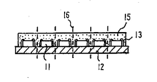
図1は、MAPと呼ばれる一括封止型半導体装置の断面図である。半導体素子11が基板12に高密度実装されており、両者は金線13によって電気接続されている。又、半導体素子は樹脂組成物15によって封止された後、個々の半導体装置に破線16で切断される。最終的に個々の半導体装置は母基板に実装され電子部品の一部となる。
FIG. 1 is a cross-sectional view of a batch sealed semiconductor device called MAP. The semiconductor element 11 is mounted on the
図2は、本発明による一括封止型半導体装置の樹脂封止方法の一例を示す模式図である。樹脂組成物21は予め剥離紙22に塗布された積層材料である。圧縮成形機29には熱盤28及び金型(25,26)が搭載されている。一括封止型半導体基板23は上型25に、積層材料は下型26に配置されている。これらは圧縮成形法により一体化及び硬化された後に個々の半導体装置に切断され製品となる。
FIG. 2 is a schematic view showing an example of a resin sealing method for a batch sealing type semiconductor device according to the present invention. The
図3は、本発明のエポキシ樹脂組成物の形状の一例を示す。図3(a)は、エポキシ樹脂組成物の上面図である。樹脂組成物21が全面に形成されている。図3(b)は、図3(a)のA−A‘断面図である。剥離紙22の上に樹脂組成物21が形成されている。樹脂組成物21は、中央部が凸状になるように形成されている。
FIG. 3 shows an example of the shape of the epoxy resin composition of the present invention. FIG. 3A is a top view of the epoxy resin composition. A
図4は、本発明のエポキシ樹脂組成物の形状の他の例を示す。図4(a)は、エポキシ樹脂組成物の上面図である。樹脂組成物21が全面に形成され切り込み31が格子状に設けられている。図4(b)は、図4(a)のA−A‘断面図である。剥離紙22の上に樹脂組成物21が形成されている。樹脂組成物21にはほぼV字型の切り込み31が設けられている。
FIG. 4 shows another example of the shape of the epoxy resin composition of the present invention. FIG. 4A is a top view of the epoxy resin composition. The
図5は、本発明のエポキシ樹脂組成物の形状の他の例を示す。図5(a)は、エポキシ樹脂組成物の上面図である。樹脂組成物21が複数個のブロック32の集合体として剥離紙22の上に形成されている。図5(b)は、図5(a)のA−A‘断面図である。剥離紙22の上に複数のブロック32に分けて樹脂組成物21が形成されている。隣り合うブロック32は隙間33を持って配置されている。
FIG. 5 shows another example of the shape of the epoxy resin composition of the present invention. FIG. 5A is a top view of the epoxy resin composition. The
本発明は、一括封止型半導体装置の樹脂封止方法を提供するものである。従来法での成形時の問題を解決する工業的な製造方法である。本発明の樹脂封止方法により一括封止型半導体装置を汎用化することができる。 The present invention provides a resin sealing method for a batch sealing type semiconductor device. It is an industrial manufacturing method that solves the problems during molding in the conventional method. The encapsulated semiconductor device can be generalized by the resin sealing method of the present invention.
又、エポキシ組成物の形状を中央を凸型にしたり、エポキシ組成物にほぼV字形の切り込みを設けたり、エポキシ組成物を複数のブロックにして隙間を入れ配置することでボイドを容易に外部に排出できる。 In addition, the voids can be easily set to the outside by making the center of the epoxy composition convex, providing V-shaped cuts in the epoxy composition, or arranging the epoxy composition in multiple blocks with gaps. Can be discharged.
以下、本発明を樹脂組成物の製法例、樹脂封止の実施例及び比較例にて具体的に説明する。 Hereinafter, the present invention will be specifically described with examples of resin composition production, resin-sealing examples and comparative examples.
樹脂組成物Aの製法
球状シリカ88部(SE−8N、トクヤマ)、エポキシ樹脂6部(828、油化シェルエポキシ)、酸無水物4部(Me−THPA、新日本理化)硬化促進剤0.2部(1B2MZ、四国化成)、カップリング剤0.5部(KBM−303、信越化学工業)及び顔料0.1部(MA600、三菱化学)を混合した後、加熱ニーダを用いて10分間混練した。
Production method of resin composition A Spherical silica 88 parts (SE-8N, Tokuyama), epoxy resin 6 parts (828, oiled shell epoxy),
一括封止型半導体基板及び樹脂組成物Aを図2のように配置した後、圧縮成形し図1のような一括封止型半導体装置を試作した。本例では問題となるような未充填や金線変形及び反り現象は認められなかった。又、中央を凸状にした樹脂組成物で一括封止するとボイドの発生はなかった。 The batch-sealed semiconductor substrate and the resin composition A were arranged as shown in FIG. 2, and then compression molded to produce a batch-sealed semiconductor device as shown in FIG. In this example, no unfilling, gold wire deformation, and warp phenomenon, which cause problems, were observed. In addition, when the center was sealed with a resin composition having a convex center, no void was generated.
比較例1として、固形エポキシ樹脂組成物Bを組成した。 As Comparative Example 1, a solid epoxy resin composition B was prepared.
球状シリカ80部(FB35 56部、デンカ、ZA−30 16部、龍森、SO−E2 8部、アドマテックス)、エポキシ樹脂部12部(EPPN501 8部、EOCN 4部、日本化薬)硬化剤6部(H−1、明和化成)、硬化促進剤0.16部(TPP,北興化学)、カップリング剤0.8部(KBM403、信越化学)、離型剤0.2部(ヘキストE、ヘキスト)、難燃化剤2部(Sb2O3、三国製錬)
実施例と同じ一括封止型半導体基板を固形エポキシ樹脂組成物Bを用いて従来の移送成形法にて樹脂封止したところ、流動性不足に起因する不良(未充填や金線変形)を10%以上発生した。
Spherical silica 80 parts (FB35 56 parts, Denka, ZA-30 16 parts, Tatsumori, SO-E2 8 parts, Admatex),
When the same encapsulated semiconductor substrate as in the example was resin-sealed by the conventional transfer molding method using the solid epoxy resin composition B, 10 defects due to insufficient fluidity (unfilled or gold wire deformation) were observed. % Or more occurred.
比較例2として、液状組成物Cを組成した。 As Comparative Example 2, a liquid composition C was prepared.
球状シリカ74部(FB35 57部、龍森、SO−E2 17部、アドマテックス)、エポキシ樹脂12部(EPC830LVP、DIC)、硬化剤12部(HN5500、日立化成)、硬化促進剤0.2部(1MZ,四国化成)、カップリング剤 0.6部(KBM403、信越化学)、難燃化剤2部(Sb2O3、三国製錬)
樹脂組成物Aの代わりに従来の液状樹脂組成物Cを用いて実施例と同様に樹脂封止した。この場合、下型に剥離紙を敷きその上に樹脂組成物を塗布した。成形後に取り出した一括封止型半導体装置はお椀のような大きな反りが生じた。
Spherical silica 74 parts (FB35 57 parts, Tatsumori, SO-E2 17 parts, Admatex),
Instead of the resin composition A, a conventional liquid resin composition C was used and sealed in the same manner as in the example. In this case, a release paper was laid on the lower mold and the resin composition was applied thereon. The packaged semiconductor device taken out after the molding was warped like a bowl.
11 半導体素子
12 基板
13 金線
15、21 樹脂組成物
16 切断面を示す破線
22 剥離紙
23 一括封止型半導体基板(半導体素子集合搭載基板)
25、26 金型
28 熱盤
29 圧縮成形機
31 切り込み
32 ブロック
33 隙間
DESCRIPTION OF SYMBOLS 11
25, 26
Claims (7)
Priority Applications (1)
| Application Number | Priority Date | Filing Date | Title |
|---|---|---|---|
| JP2003274848A JP4270969B2 (en) | 2002-07-16 | 2003-07-15 | Resin sealing method for semiconductor device |
Applications Claiming Priority (2)
| Application Number | Priority Date | Filing Date | Title |
|---|---|---|---|
| JP2002207421 | 2002-07-16 | ||
| JP2003274848A JP4270969B2 (en) | 2002-07-16 | 2003-07-15 | Resin sealing method for semiconductor device |
Publications (2)
| Publication Number | Publication Date |
|---|---|
| JP2004056141A JP2004056141A (en) | 2004-02-19 |
| JP4270969B2 true JP4270969B2 (en) | 2009-06-03 |
Family
ID=31949492
Family Applications (1)
| Application Number | Title | Priority Date | Filing Date |
|---|---|---|---|
| JP2003274848A Expired - Lifetime JP4270969B2 (en) | 2002-07-16 | 2003-07-15 | Resin sealing method for semiconductor device |
Country Status (1)
| Country | Link |
|---|---|
| JP (1) | JP4270969B2 (en) |
Families Citing this family (6)
| Publication number | Priority date | Publication date | Assignee | Title |
|---|---|---|---|---|
| DE102007012155B4 (en) | 2007-03-12 | 2015-01-22 | Intel Mobile Communications GmbH | Shaped bodies and benefits with semiconductor chips and method of making the benefit |
| JP5086945B2 (en) | 2008-09-05 | 2012-11-28 | 株式会社東芝 | Manufacturing method of semiconductor device |
| JP2015035523A (en) * | 2013-08-09 | 2015-02-19 | 日東電工株式会社 | Group of separator-provided resin sheet for sealing electronic device and method for selecting separator-provided resin sheet for sealing electronic device |
| JP6793517B2 (en) | 2016-10-17 | 2020-12-02 | 株式会社ダイセル | Sheet prepreg |
| JP7282535B2 (en) | 2019-01-28 | 2023-05-29 | 株式会社ダイセル | Sheet prepreg for encapsulating fan-out packages |
| JP7482715B2 (en) * | 2019-08-23 | 2024-05-14 | ナガセケムテックス株式会社 | Method for manufacturing sealing structure |
-
2003
- 2003-07-15 JP JP2003274848A patent/JP4270969B2/en not_active Expired - Lifetime
Also Published As
| Publication number | Publication date |
|---|---|
| JP2004056141A (en) | 2004-02-19 |
Similar Documents
| Publication | Publication Date | Title |
|---|---|---|
| JP5397195B2 (en) | Manufacturing method of substrate for mounting optical semiconductor element and manufacturing method of optical semiconductor device | |
| WO2015005275A1 (en) | Process for producing semiconductor devices, and semiconductor device | |
| KR20090082344A (en) | Epoxy resin composition for semiconductor encapsulation and semiconductor device | |
| TW200830490A (en) | High thermal performance packaging for circuit dies | |
| JP5617495B2 (en) | Semiconductor device manufacturing method and semiconductor device | |
| JP5228453B2 (en) | Semiconductor device and sealing resin composition | |
| JP4569137B2 (en) | Semiconductor sealing resin composition and semiconductor device | |
| JP4270969B2 (en) | Resin sealing method for semiconductor device | |
| KR100663680B1 (en) | Epoxy resin composition and semiconductor device | |
| JP2019026715A (en) | Epoxy resin composition for collectively sealing, electronic device and method for manufacturing the same | |
| JP2006008956A (en) | Resin composition for sealing semiconductor and semiconductor device using the same | |
| JP3406073B2 (en) | Resin-sealed semiconductor device | |
| JP4710200B2 (en) | Manufacturing method of area mounting type semiconductor sealing epoxy resin composition and area mounting type semiconductor device | |
| JPS63230725A (en) | Epoxy resin composition for semiconductor sealing | |
| JPH08162573A (en) | Semiconductor device | |
| JP3347228B2 (en) | Semiconductor device | |
| JP2000022049A (en) | Resin-sealed semiconductor device and epoxy resin composition for sealing the same | |
| JP7434794B2 (en) | Manufacturing method of semiconductor device and epoxy resin composition for sealing | |
| KR102352497B1 (en) | Thermosetting resin composition, resin encapsulating substrate and electronic device | |
| JP3915545B2 (en) | Epoxy resin composition for sealing and single-side sealed semiconductor device | |
| JP2000239355A (en) | Epoxy resin composition and semiconductor device | |
| KR20200127043A (en) | Particulate encapsulation resin composition, semiconductor device, and manufacturing method thereof | |
| JPH0794640A (en) | Manufacture of resin sealed semiconductor device | |
| KR19990036775A (en) | Encapsulation material and lead-on-chip structure semiconductor device using the same | |
| JP3956717B2 (en) | Epoxy resin composition for sealing and single-side sealed semiconductor device |
Legal Events
| Date | Code | Title | Description |
|---|---|---|---|
| A621 | Written request for application examination |
Free format text: JAPANESE INTERMEDIATE CODE: A621 Effective date: 20060712 |
|
| A977 | Report on retrieval |
Free format text: JAPANESE INTERMEDIATE CODE: A971007 Effective date: 20080811 |
|
| A131 | Notification of reasons for refusal |
Free format text: JAPANESE INTERMEDIATE CODE: A131 Effective date: 20080814 |
|
| A521 | Request for written amendment filed |
Free format text: JAPANESE INTERMEDIATE CODE: A523 Effective date: 20081008 |
|
| A521 | Request for written amendment filed |
Free format text: JAPANESE INTERMEDIATE CODE: A523 Effective date: 20081031 |
|
| TRDD | Decision of grant or rejection written | ||
| A01 | Written decision to grant a patent or to grant a registration (utility model) |
Free format text: JAPANESE INTERMEDIATE CODE: A01 Effective date: 20090203 |
|
| A01 | Written decision to grant a patent or to grant a registration (utility model) |
Free format text: JAPANESE INTERMEDIATE CODE: A01 |
|
| A61 | First payment of annual fees (during grant procedure) |
Free format text: JAPANESE INTERMEDIATE CODE: A61 Effective date: 20090224 |
|
| FPAY | Renewal fee payment (event date is renewal date of database) |
Free format text: PAYMENT UNTIL: 20120306 Year of fee payment: 3 |
|
| R150 | Certificate of patent or registration of utility model |
Ref document number: 4270969 Country of ref document: JP Free format text: JAPANESE INTERMEDIATE CODE: R150 Free format text: JAPANESE INTERMEDIATE CODE: R150 |
|
| FPAY | Renewal fee payment (event date is renewal date of database) |
Free format text: PAYMENT UNTIL: 20120306 Year of fee payment: 3 |
|
| FPAY | Renewal fee payment (event date is renewal date of database) |
Free format text: PAYMENT UNTIL: 20130306 Year of fee payment: 4 |
|
| R250 | Receipt of annual fees |
Free format text: JAPANESE INTERMEDIATE CODE: R250 |
|
| FPAY | Renewal fee payment (event date is renewal date of database) |
Free format text: PAYMENT UNTIL: 20130306 Year of fee payment: 4 |
|
| FPAY | Renewal fee payment (event date is renewal date of database) |
Free format text: PAYMENT UNTIL: 20140306 Year of fee payment: 5 |
|
| R250 | Receipt of annual fees |
Free format text: JAPANESE INTERMEDIATE CODE: R250 |
|
| R250 | Receipt of annual fees |
Free format text: JAPANESE INTERMEDIATE CODE: R250 |
|
| R250 | Receipt of annual fees |
Free format text: JAPANESE INTERMEDIATE CODE: R250 |
|
| R250 | Receipt of annual fees |
Free format text: JAPANESE INTERMEDIATE CODE: R250 |
|
| R250 | Receipt of annual fees |
Free format text: JAPANESE INTERMEDIATE CODE: R250 |
|
| R250 | Receipt of annual fees |
Free format text: JAPANESE INTERMEDIATE CODE: R250 |
|
| R250 | Receipt of annual fees |
Free format text: JAPANESE INTERMEDIATE CODE: R250 |
|
| R250 | Receipt of annual fees |
Free format text: JAPANESE INTERMEDIATE CODE: R250 |
|
| R250 | Receipt of annual fees |
Free format text: JAPANESE INTERMEDIATE CODE: R250 |
|
| R250 | Receipt of annual fees |
Free format text: JAPANESE INTERMEDIATE CODE: R250 |
|
| R250 | Receipt of annual fees |
Free format text: JAPANESE INTERMEDIATE CODE: R250 |
|
| EXPY | Cancellation because of completion of term |