JP4265732B2 - Lamp lighting device and projector using the same - Google Patents
Lamp lighting device and projector using the same Download PDFInfo
- Publication number
- JP4265732B2 JP4265732B2 JP2002154874A JP2002154874A JP4265732B2 JP 4265732 B2 JP4265732 B2 JP 4265732B2 JP 2002154874 A JP2002154874 A JP 2002154874A JP 2002154874 A JP2002154874 A JP 2002154874A JP 4265732 B2 JP4265732 B2 JP 4265732B2
- Authority
- JP
- Japan
- Prior art keywords
- lamp
- lighting device
- circuit
- resistor
- voltage
- Prior art date
- Legal status (The legal status is an assumption and is not a legal conclusion. Google has not performed a legal analysis and makes no representation as to the accuracy of the status listed.)
- Expired - Fee Related
Links
- 230000001052 transient effect Effects 0.000 claims description 24
- 239000011347 resin Substances 0.000 claims description 19
- 229920005989 resin Polymers 0.000 claims description 18
- 230000007704 transition Effects 0.000 claims description 7
- 230000000630 rising effect Effects 0.000 claims description 4
- 239000004065 semiconductor Substances 0.000 claims description 3
- 239000000463 material Substances 0.000 claims description 2
- 208000028659 discharge Diseases 0.000 description 50
- 238000010586 diagram Methods 0.000 description 12
- 150000001875 compounds Chemical class 0.000 description 11
- 238000004804 winding Methods 0.000 description 6
- 239000003990 capacitor Substances 0.000 description 5
- 238000009499 grossing Methods 0.000 description 5
- 230000020169 heat generation Effects 0.000 description 4
- 239000004973 liquid crystal related substance Substances 0.000 description 4
- 238000009826 distribution Methods 0.000 description 3
- 230000000694 effects Effects 0.000 description 3
- 239000011810 insulating material Substances 0.000 description 3
- 230000001360 synchronised effect Effects 0.000 description 3
- 230000015556 catabolic process Effects 0.000 description 2
- QSHDDOUJBYECFT-UHFFFAOYSA-N mercury Chemical compound [Hg] QSHDDOUJBYECFT-UHFFFAOYSA-N 0.000 description 2
- 229910052753 mercury Inorganic materials 0.000 description 2
- 229910001507 metal halide Inorganic materials 0.000 description 2
- 150000005309 metal halides Chemical class 0.000 description 2
- 230000004048 modification Effects 0.000 description 2
- 238000012986 modification Methods 0.000 description 2
- 150000003377 silicon compounds Chemical class 0.000 description 2
- 229910052724 xenon Inorganic materials 0.000 description 2
- FHNFHKCVQCLJFQ-UHFFFAOYSA-N xenon atom Chemical compound [Xe] FHNFHKCVQCLJFQ-UHFFFAOYSA-N 0.000 description 2
- 241001270131 Agaricus moelleri Species 0.000 description 1
- XEEYBQQBJWHFJM-UHFFFAOYSA-N Iron Chemical group [Fe] XEEYBQQBJWHFJM-UHFFFAOYSA-N 0.000 description 1
- 230000003321 amplification Effects 0.000 description 1
- 238000006243 chemical reaction Methods 0.000 description 1
- 230000000593 degrading effect Effects 0.000 description 1
- 238000001514 detection method Methods 0.000 description 1
- 238000010891 electric arc Methods 0.000 description 1
- 230000017525 heat dissipation Effects 0.000 description 1
- 229910052751 metal Inorganic materials 0.000 description 1
- 239000002184 metal Substances 0.000 description 1
- 238000000034 method Methods 0.000 description 1
- 238000003199 nucleic acid amplification method Methods 0.000 description 1
- 238000004382 potting Methods 0.000 description 1
- 229920006395 saturated elastomer Polymers 0.000 description 1
- 238000004904 shortening Methods 0.000 description 1
- 230000003595 spectral effect Effects 0.000 description 1
- 238000003860 storage Methods 0.000 description 1
Images

Landscapes
- Circuit Arrangements For Discharge Lamps (AREA)
- Projection Apparatus (AREA)
- Transforming Electric Information Into Light Information (AREA)
Description
【0001】
【発明の属する技術分野】
本発明はランプ点灯装置及びこれを用いたプロジェクタに関し、特に、液晶デバイスやDMD(Digital Mirror Device)を用いたプロジェクタに用いられる放電ランプの点灯装置に関する。
【0002】
【従来の技術】
液晶デバイスやDMDを用いて画像を光学的に投射し表示させるプロジェクタの光源として、キセノンランプ、メタルハライドランプ、超高圧水銀ランプなどの放電ランプが用いられている。これらの放電ランプは、そのガスや金属によって分光分布、輝度分布、配光分布、電気特性等を異にし、プロジェクタの設計仕様に適したランプが選択される。また、放電ランプの電極は、ショートアークランプが望ましく、これは非常に高い放射輝度を発生することによる。
【0003】
一般に放電ランプを点灯させるには、(1)ランプ起動時にランプ電極間に高電圧を印加して絶縁破壊を起こし放電路を形成するステップ、(2)ランプの電極間にグロー放電電流を流しアーク放電に移行させるステップ、(3)アーク放電を安定化させそれを維持するステップを必要とする。このため、放電ランプを点灯させる点灯装置は、放電ランプの起動を行うイグナイタ回路と放電ランプへ安定的に電力を供給する回路とを含んで構成される。
【0004】
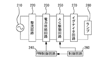
図8は従来のプロジェクタに用いられる一般的なランプ点灯方式の一構成例を示すブロック図である。同図において、ランプ点灯装置は、交流電源210からの交流電圧を整流・平滑化する整流・平滑化回路220、放電ランプ280に安定的な電力を供給する電力供給回路230、電力供給回路230の電力供給を制御するPWM制御回路240、放電ランプ280をAC駆動するAC駆動回路250、各部の制御を行う制御回路部260、および放電ランプ280の起動(若しくは点火)を行うためのイグナイタ回路270を含む。
【0005】
交流電源210からの交流電圧は整流・平滑化回路210により直流電圧に変換され、この直流電圧は、PWM制御回路240の制御により電力供給回路230において昇圧または降圧される。電力供給回路230の出力端はAC駆動回路250に接続され、制御部260は、PWM制御回路240およびAC駆動回路250を制御し、放電ランプ280を起動させかつAC駆動させる。
【0006】
【発明が解決しようとする課題】
しかしながら、従来のランプ点灯装置には次のような課題がある。図9にイグナイタ回路270の一構成例を示す。放電ランプ280の起動時、PWM制御回路240によって制御された電力供給回路230は約250ないし370ボルトの電圧を供給し、この電圧はAC駆動回路250を介してイグナイタ回路270に供給される。AC駆動回路250の高電位側出力からダイオード271を介してコンデンサ272に電流が蓄積され、この電圧が一定値を超えるとトリガー素子273が導通し、トランス274の一次側コイルに電流が流され、これによって二次側コイルに発生された電流がダイオード275を介してコンデンサ276に充電される。コンデンサ276の電圧がバリスタ277のしきい値を越えると、トランス278の一次側コイルに電流が流れ、これによって二次側コイルに非常に高い十数キロボルトの電圧が発生される。そして、放電ランプ280の端子間に絶縁破壊が生じ、グロー放電が開始される。
【0007】
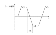
放電ランプ280の起動(点火)後、電力供給回路230の出力端はランプ放電初期電圧に降圧され、その直流電圧はAC駆動回路250によって交流電圧に変換され、放電ランプ280のAC駆動が行われる。AC駆動回路250の出力端と放電ランプ280との間の電流通路内には、トランス278の二次側コイルLaが介在し(あるいは、これ以外にノイズ除去用のインダクター、共振用インダクターあるいは電力蓄積用のインダクターが存在することがある)、インダクターLaの介在により、リンギング、オーバーシュートあるいはアンダーシュートが生じ、図10に示すようにランプ駆動電流の過渡応答時間が緩やかとなる。すなわちランプ駆動電流の立上りと立下りが緩やかとなり、結果としてその立上りと立下がり期間Tdが長くなってしまう。期間Tdが長くなると、放電ランプの光量に明暗が発生し、この状態でプロジェクタの光源に使用されると、投影画像にチラツキが発生したり、またプロジェクタの映像同期信号H、Vとの関係で、映像にビート等の映像ノイズが生じたり、グレースケールにおいてはスムースな階調等を再現することができないという課題がある。
【0008】
特に、単板式DLPを用いたプロジェクタにおいて、放電ランプ280のAC駆動のタイミングは、放電ランプの白色光からR、G、B(又はRGBW)の波長の光を取り出すタイミングと同期させる必要がある。つまり、R、G、Bのカラーフィルターを配列したカラーホイールを回転させ、これに放電ランプからの白色光を入射させるとき、カラーフィルターの境界において必ずしもR、G、Bの純粋な波長が得られず混在した波長が存在するため、この境界部分とランプ駆動電流の極性を反転させるタイミングとを同期させている。このため、インダクターによるランプ駆動電流の立上りや立下りが緩やかでその期間Td時間が長いと、その期間において有効な光量を得ることができない等不便であった。また、ランプのAC駆動周波数をカラーフィルターの回転と同期させる必要があるため、ランプの最適駆動周波数に合わせることができなく、ランプ寿命の短命化やアークのチラツキ等が発生するといった不都合があった。
【0009】
そこで本発明は上記従来技術の課題を解決し、ランプのAC駆動時においてランプ駆動電流の過渡応答時間を速くしたランプ点灯装置を提供することを目的とする。
本発明の他の目的は、ランプ駆動電流の立上りと立下りを急峻にし、立上りと立下りの期間を映像処理時間に比較して十分に短くでき、またオーバーシュートやリンギング等を軽減することができるようなランプ点灯装置およびこれを用いたプロジェクタを提供することである。
本発明の他の目的は、映像信号についての画像処理時間やカラーフィルターの動作と非同期で動作可能なランプ点灯装置を提供することである。
本発明の他の目的は、ランプの寿命や特性に合った最適周波数でランプをAC駆動することが可能なランプ点灯装置を提供することである。
本発明に他の目的は、投射映像にチラツキや映像ノイズの発生を抑制したプロジェクタを提供することである。
【0010】
【課題を解決するための手段】
本発明に係るランプ点灯装置は、交流電圧をランプに印加してランプの交流駆動を行うものであって、電流経路に接続されたランプと、前記ランプの起動時に前記電流経路を介して前記ランプに高電圧を印加するイグナイタ回路と、前記ランプの交流駆動時に前記電流経路を介して前記ランプに交流電圧を印加する交流駆動回路と、前記イグナイタ回路は、高電圧を発生させるためのトランスを含み、当該トランスの2次側のインダクターが前記ランプに直列に接続されており、前記交流駆動回路は、直流電圧を交流電圧に変換するCMOSインバータ回路を含み、CMOSインバータ回路からの出力が前記電流経路に接続されており、ランプ点灯装置はさらに、前記電流経路内において前記2次側のインダクターと直列に接続される少なくとも1つの抵抗と、前記少なくとも1つの抵抗と並列に接続されるスイッチ手段とを有し、前記スイッチ手段は、前記イグナイタ回路により前記ランプを起動するとき前記少なくとも1つの抵抗が短絡されるようにスイッチを閉じ、前記交流駆動回路により前記ランプを交流駆動するとき、前記交流駆動回路の交流駆動電圧の周波数に同期し、交流駆動電圧の立ち上がりと立下りとの間の過渡期間において前記少なくとも1つの抵抗が接続されるようにスイッチを開く。好ましくは前記CMOSインバータ回路は、前記過渡期間において、トランジスタがオフする期間を含み、前記スイッチ手段は、前記オフする期間よりも長い期間だけスイッチを開く。
【0011】
好ましくは前記2次側のインダクターと前記少なくとも1つの抵抗とを含む電流通路における過渡応答時の時定数を20マイクロ秒以下にする。実験的および経験則から20マイクロ秒以下の時定数とすることで、RL直列回路における過渡現象が速く収束する。つまり、ランプへの駆動電流の立上り・立下りが速くなり、その期間Tdを小さくすることができる。またこれによって、映像同期信号(H、V)との関係により映像ノイズを無視することができる。
【0012】
前記トランスおよび前記少なくとも1つの抵抗は、前記インダクターの巻線抵抗値を選択することにより得るようにしてもよい。巻線抵抗値は、おおよそ1オーム以下に選定されることが望ましい。これは、発熱及び高圧印加時において抵抗による電力の損失を防ぐためである。
【0013】
前記トランス及び前記少なくとも1つの抵抗は絶縁性樹脂コンパウンド内に収容されるようにしてもよい。絶縁性樹脂コンパウンドは、例えはシリコンコンパウンドである。抵抗は、インダクターの巻線抵抗であっても、それに代えて別個に抵抗を設けてもよい。抵抗値は1オーム以下であることが望ましい。抵抗が大きいと、そこを流れる電流による発熱が生じ、その部分の熱膨張が原因でコンパウンドにクラックが生じてしまうからである。
【0015】
前記外部抵抗の抵抗値は前記絶縁性樹脂内の抵抗の抵抗値の少なくとも10倍以上であることが望ましい。絶縁性樹脂内の抵抗を小さくして樹脂内での発熱を小さくし、外部抵抗によって時定数を小さくし、過渡応答を速くする。
【0016】
本発明では、抵抗と並列にスイッチ手段が接続され、該スイッチ手段は前記交流駆動電圧の周波数に同期し、前記交流駆動電圧の過渡期間中に抵抗に電流を流させる。つまり、交流電圧の過渡期間中に抵抗を働かせ、駆動電流の立上り・立下りを急峻にし、それ以外の期間は抵抗を短絡させ、無駄な損失を抑制する。前記スイッチ手段は、半導体スイッチング素子を用いることができ、好ましくはGTOサイリスタを用いることができる。但し、それ以外にMOSトランジスタやバイポーラトランジスタ等を使用しても良い。
【0018】
前記電流経路にはさらに、ノイズを除去するためのインダクター、前記ランプの駆動時に電力を蓄積可能なインダクター、および共振用インダクターの少なくとも1つが接続されるようにしてもよい。
【0020】
好ましくは前記ランプ点灯装置は、光を投射するプロジェクタに用いられる。プロジェクタは、例えば、ランプと、前記ランプを点灯させるためのランプ点灯装置と、前記ランプからの光を少なくともR、G、Bの波長を有する光に分別する分別手段と、前記分別手段からの光を変調する変調手段と、前記変調手段によって変調された光を投射する投射手段とを備える。
【0021】
ランプ点灯装置におけるAC駆動電流の立上り・立下りを急峻にすることで、ランプの光量ムラを抑制し、投影画像のチラツキや映像ノイズを抑制した鮮明な画像を映し出すことができる。
【0022】
上記の駆動回路は分別手段と非同期に動作される。好ましくは、分別手段は、少なくともR、G、Bの波長の光を分別可能なカラーフィルターを備え、該カラーフィルターを回転させることにより前記ランプからの光を順次R、G、Bの光に変換する。また変調手段は、ライトバルブを含み、該ライトバルブはDMDである。
【0023】
駆動回路を分別手段と非同期とすることで、駆動回路におけるAC駆動電流の周波数は、カラーホイールの回転動作による制約を受けないため、ランプの寿命や特性に合った最適周波数を設定することができる。
【0024】
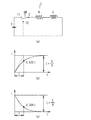
次に本発明の基本的概念およびその作用について説明する。図1(a)は、本発明に係るランプ点灯装置においてAC駆動されるランプに接続された電流通路にインダクターと抵抗とを含む回路を等価的なRL直列回路で表したものである。
【0025】
RL直列回路1は、電源Eと直列に接続された抵抗R、インダクターL、及びスイッチSWとを有する。スイッチSWの共通端子Cを端子T1または端子T2に切り替えることでRL直列回路に過渡現象が生じ、これはランプを交流駆動するときの電流通路のインダクター及び抵抗の過渡現象と等価である。
【0026】
RL直列回路1においてスイッチSWのコモン端子Cが端子T1に接続されると、電源EからR、Lへ向けて電流iが流れ、その過渡応答は次式により表される。
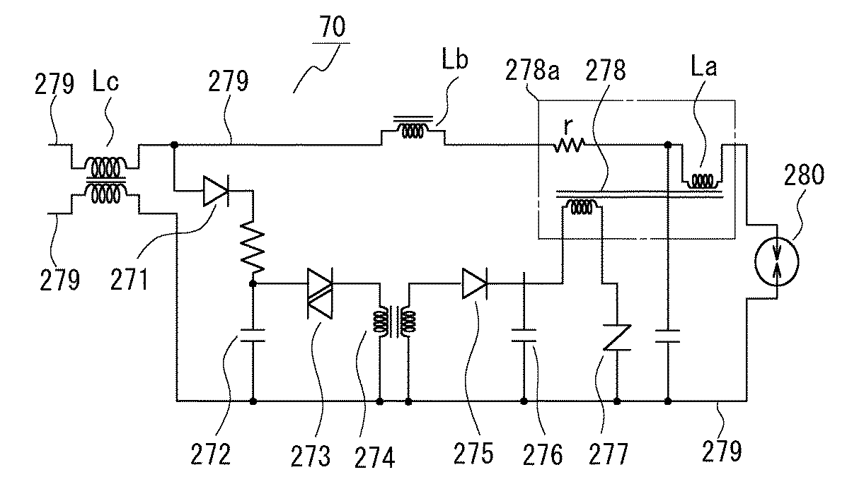
図1(b)は(2)式の指数曲線を示し、T=L/Rのとき、電流iが63.2%の大きさにある。時定数Tの値が小さいほど、過渡現象が速く収束することがわかる。言い換えれば、Rを大きくすれば、T=L/Rが小さくなり過渡応答が速くなる。
【0027】
次に、スイッチSWのコモン端子Cを端子T2に接続すると、上記とは反対方向に電流iが流れ、そのときの過渡応答は(3)式で表される。
【0028】
本発明では、上記RL直列回路1における過渡現象あるいは過渡応答をランプ点灯装置に適用する。すなわち、本発明に係るランプ点灯装置において、ランプに交流駆動電流を印加する電流通路内に含まれるインダクターと直列に抵抗を設けることによって、交流駆動電流の立上り・立下りを急峻にし、その過渡応答を速くするものである。
【0029】
【発明の実施の形態】
以下、本発明の実施の形態について図面を参照して詳細に説明する。
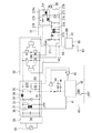
図2は、本発明の第1の実施の形態に係るランプ点灯装置の回路を示す図である。第1の実施の形態に係るランプ点灯装置は、いわゆるAC点灯方式であり、交流電源10からの交流電圧を整流・平滑化する整流・平滑化回路20と、平滑化された直流電圧を降圧し放電ランプへの電力を供給する電力供給回路30と、電力供給回路30の電力供給を制御するPWM制御回路40と、電力供給回路30から供給される直流電圧を交流電圧に変換しこれによって放電ランプのAC駆動を行うAC駆動回路50と、各回路を制御する制御部60と、放電ランプの起動時に高電圧を放電ランプに印加するイグナイタ回路70と、放電ランプ80とを含む。好ましくは、ランプ点灯装置は、液晶デバイスやDLPデバイスを利用したプロジェクタの光源部に用いられ、放電ランプには、キセノンランプ、メタルハライドランプ、超高圧水銀ランプなど使用される。
【0030】
電力供給回路30は、MOSトランジスタ31、パルストランス32、ダイオード33、インダクター(コイル)34、コンデンサ35等を含む。MOSトランジスタ31のゲートはパルストランス32の二次側コイルに接続され、その一次側コイルはPWM制御回路30のPWM出力信号41に接続される。PWM出力信号41から出力されるパルス信号に応答してMOSトランジスタ21のオン・オフが制御され、直流電圧の降圧が行われる。インダクター34及びコンデンサ35は、変圧された直流電圧から脈動する成分を取り除き平滑化された直流電圧を供給する。
【0031】
PWM制御回路40は、コントロールユニット42、電力演算回路43、増幅回路44を含む。コントロールユニット42は、スイッチSW1を閉じることによって動作を開始し、スイッチSW1は制御部60からの制御信号61によって制御される。増幅回路44の入力は、電流検出用の抵抗R1の一端に接続され電力供給回路30におけるランプ電流を検知し、これを電力演算回路43へ出力する。また電力演算回路43の他方の入力には、電源ライン間を抵抗R2、R3で分割して検出されたランプ電圧が入力される。コントロールユニット42は、電力演算回路43によって演算された電力情報に基づき放電ランプ80の動作に必要な電力が供給されるように電力供給回路30を制御する。
【0032】
AC駆動回路50は、電力供給回路30に接続され、直流電圧を交流電圧に変換するためのCMOSトランジスタQ1、Q2とQ3、Q4とを有する。CMOSトランジスタQ1、Q2と、CMOSトランジスタQ3、Q4により一対のCMOSインバータを構成し、それらのゲート電極は制御部60からの駆動信号64を介して相補的に駆動される。従って、トランジスタQ1、Q4がオンするときトランジスタQ2、Q3がオフであり、反対にトランジスタQ2、Q3がオンするとき、トランジスタQ1、Q4がオフである。こうして電力供給回路30からの直流電圧は各インバータによって交流電圧に変換され、放電ランプ80に印加される。直流−交流の変換周波数は制御部60からの駆動信号のパルス周波数を可変することによって任意に選択することが可能である。
【0033】
制御部60は、スイッチSW1のオン、オフを制御する制御信号61、コンバータ同期信号63に基づきAC駆動回路50を駆動制御する駆動信号64とを出力する。さらに制御部60は各部の動作を制御するためのタイマー回路、シーケンス回路等を含む。
【0034】
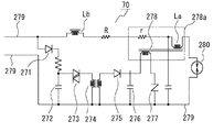
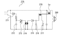
各インバータの出力は、イグナイタ回路70に接続される。イグナイタ回路70は、放電ランプ80の起動(着火)時に高電圧を発生させるパルストランス274、278およびその他の回路素子を含み、また、放電ランプ80のAC駆動時に交流電流を放電ランプ80に供給するための電流通路279を含む。
【0035】
本実施の形態では、放電ランプ80に直列接続されたパルストランス278の二次側インダクターLaに直列に接続される抵抗rを付加し、放電ランプ80のAC駆動時におけるRL直列回路の過渡応答を速くさせる。上述したようにRL直列回路の時定数をT=L/rとすることで、放電ランプ80に印加される交流駆動電流の立上がり及び立下りを急峻にすることが可能である。時定数Tは、本発明者による実験的及び経験則から20μ秒以下であることが望ましく、インダクターLaと抵抗rを適宜選択することで時定数を決定する。
【0036】
イグナイタ回路70は、好ましくは絶縁性の樹脂等(例えばシリコンコンパウンド)によってポッテイングされ、外部と電気的に絶縁される。あるいは図2の破線で示すように、選択的にコイル278を含む部分をポッテイングして樹脂コンパウンド部分(樹脂ポッテイング部分)278aを形成するようにしても良い。
【0037】
抵抗rは、絶縁性樹脂材でポッテイングされた部分278a内に挿入することができる。この場合、インダクターLaと個別に抵抗rを設けることも可能であるが、インダクターLaの巻線を調整しその巻線の内部抵抗値から得られる抵抗を抵抗rとしても良い。抵抗rは、ランプ電流の通電時に発熱し、その発熱量が大きいと樹脂コンパウンド部分278aに熱的原因によってクラック等を引き起こすおそれがある。このため、抵抗rは比較的小さな値を選択する必要があり、好ましくは、通常0.2オーム程度であり、少なくとも1オーム以下が望ましい。イグナイタ回路70のその他の構成は図9のものと基本的に同じである。
【0038】
次に、本実施の形態に係るランプ駆動装置の動作を説明する。放電ランプ80に高電圧が印加される前、スイッチSW1は開いた状態にある。交流電源10からの交流電圧が整流・平滑化回路20により直流電圧に変換され、制御部60からの制御信号61によりスイッチSW1がオンされると、PWM制御回路40からPWM出力信号41がパルストランス32へ出力され、これによってMOSトランジスタ31のオン・オフが制御される。電力供給回路30からは約250−370ボルトの直流電圧が供給され、このときAC駆動回路50は、制御部60によりトランジスタQ2、Q3をオン状態にされる。そしてイグナイタ回路70のトランス274、278によって10キロ−20キロボルトの高電圧が発生され、放電ランプ80がグロー放電を開始する。
【0039】
電力演算回路43によりランプ動作電圧P3が検出されると、PWM出力信号41によりMOSトランジスタ31が制御され、電力供給回路30から降圧された直流電圧が供給される。放電初期時はランプ動作電圧が低いためランプが安全に動作できる電流制御を行い、その後、温度上昇と共にランプ動作電圧が上昇(例えば65ボルト)した時点で電力(ワット)制御に切り替える。他方、制御部60は駆動信号64によりAC駆動回路50のインバータ駆動を開始させ、直流電圧を交流電圧に変換させる。これによってAC駆動回路50の出力端から電流通路279を介して放電ランプ80の電極間に交番電流あるいは交番電圧が印加される。このとき、トリガー素子273はしきい値電圧を200ボルト程度としているため、トリガー素子273は動作せず、AC駆動回路50からの交流電流がトランス274側へ流れ込むことはない。
【0040】
以上のようにインダクターLaに抵抗rを直列に接続させたことで時定数を小さくし、放電ランプ80の交流駆動電流の過渡応答を速くすることができる。言い換えれば、交流駆動される放電ランプの交流電流の立上り及び立下りを急峻にし、従来の図10に示すような期間Tdを小さくすることができる。
【0041】
上記実施の態様は、インダクターLaが電流通路279に含まれる場合を示したが、インダクターはこれに限らず電流通路279に含まれる複数のインダクターであっても良い。図3は、イグナイタ回路70の電流通路279内にインダクターLbを接続した例である。インダクターLbは、放電ランプ80のAC駆動時に電流の戻りを抑制して電力を蓄積し放電ランプ80が消えにくくさせるものである。この場合にも、時定数T=(La+Lb)/rを20マイクロ秒以下にすることが望ましい。図4は、さらにノイズ除去用の一対のインダクターLcをAC駆動回路50の出力端とイグナイタ回路70の間に設けたものである。図3及び図4に示すようなインダクターLb、Lcが電流通路279に含まれる回路においても本発明が有効に作用することは言うまでもない。さらに、上記以外のインダクターとして共振用インダクターや飽和インダクターを含むものであっても良い。
【0042】
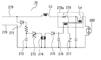
次に本発明の第2の実施の形態に係るランプ点灯装置について説明する。本実施の形態に係るイグナイタ回路70は、図5に示すように、樹脂コンパウンド278aの外部に外付けの外部抵抗Rを付加する。樹脂コンパウンド278a内の抵抗rが大きいと、その発熱量(W=I2r)が大きくなり、絶縁材でポッテイングされたコイルでは放熱の問題や、温度上昇による熱膨張係数の差から絶縁材にクラックを生じさせ絶縁材を劣化させるという問題を引き起こす。そこで、本実施の形態では、樹脂コンパウンド278aの外部に外付けの抵抗Rを直列に接続する。
【0043】
外付けの外部抵抗Rを付加することで、時定数はT=L/(R+r)となり、より時定数を小さくすることで過渡応答を速くすることができ、その一方で樹脂コンパウンド278aにおける抵抗の発熱の問題を回避することができる。なお、内部抵抗rは、巻線の内部抵抗を用いることができる。あるいは抵抗rを除去し外部抵抗Rのみを用いるようにすることも可能である。本実施の形態では、外部抵抗Rを約2オーム、内部抵抗rを約0.2オームにする。好ましくは外部抵抗の抵抗値を内部抵抗の抵抗値の少なくとも10倍以上にする。
【0044】
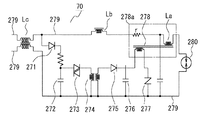
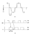
本発明の第3の実施の形態に係るイグナイタ回路を図6に示す。本実施の形態では、第2の実施の形態における外付け抵抗Rと並列にスイッチSW2を接続する。スイッチSW2は、初期点灯時からランプ電流が安定するまで閉じられ、この間外部抵抗Rをショートさせる。次にランプ電流が安定したら、スイッチSW2は図7(b)に示すようにランプの交流電圧の立上り及び立下りの過渡期間に同期して開かれ、その期間だけ外部抵抗Rに電流を流させ、抵抗Rを作用させる。これにより、時定数がT=L/(r+R)となり、ランプ電流の立下りおよび立上りが速くなる。過渡時のみ外部抵抗Rに電流を流すことで抵抗による発熱量を抑制することができ、定格電力の小さな抵抗を用いることができ、装置を小型化、安価にすることができる。
【0045】
ランプ電圧は、図7(a)に示すように過渡時に一定期間オフとなる期間Toffを含む。これは、AC駆動回路50がインバータの貫通電流を防止するためにトランジスタQ1ないしQ4をすべて一定期間オフにするためである。このため、スイッチSW2がオフする期間すなわち外部抵抗Rがオンする期間Tonは、Toffよりも大きくすることの望ましく、少なくとも期間Toffを含む期間において外部抵抗Rを時定数に寄与させることができる。
【0046】
スイッチSW2は、半導体スイッチング素子を用いても良く、例えばGTOサイリスタ(ゲート・ターンオフ・サイリスタ)を用いることが望ましい。制御部60からの制御パルス信号をGTOサイリスタのゲートに印加し、過渡期間に同期させてサイリスタをオン・オフさせることができる。あるいは、サイリスタに代えて他のスイッチング素子(バイポーラトランジスタやMOSトランジスタ)を用いることも可能である。
【0047】
また、図7(a)の波線はランプ電流を示し、AC駆動に際して電流通路279内に含まれるインダクターのインダクタンスを適切な値にすることで、電流の立上りおよび立下りを滑らかにし、電流のオーバーシュート、アンダーシュート、リンギングを抑制することができる。例えば、インダクターLaやLbの鉄心を移動させてインダクタンスを調整するようにしても良いし、あるいはインダクターと並列にスイッチを接続しAC駆動時のみ作動するインダクターを設けても良い。この場合、好ましくはランプの定格電流の2/3程度で飽和する飽和インダクターが望ましい。
【0048】
図5および図6に示す実施の形態において、電流通路279内にインダクターLbを介在させてが、必要に応じてインダクターLbを除去することも可能である。あるいは、図4に示すようなインダクターLcを単独で用いることもインダクターLbと共に用いることも可能である。
【0049】
上記第1ないし第3の実施の形態では、イグナイタ回路70に抵抗rあるいは抵抗Rを付加した例を示したが、これらの抵抗rあるいは抵抗Rは、必ずしもイグナイタ回路内に配置される必要はない。これらの抵抗は、AC駆動に際してランプに電流が印加される電流通路内にあれば、本質的に本発明の作用効果を奏するものである。さらに、本実施の形態で用いたイグナイタ回路70は一つの構成例であり、必ずしもこのような構成に限定されるものではない。インダクターについても同様に必ずしもイグナイタ回路内に配置される必要はなく、ランプに接続された電流通路内にあればよい。
【0050】
例えば、AC駆動回路50において直流電圧を交流電圧に変換するMOSトランジスタQ1、Q3の導通時のオン抵抗を適切な値に選定することも可能である。例えば、トランジスタQ1、Q3のオン抵抗をr1とすることで、時定数をT=L/r1とすることも可能である。あるいは、樹脂コンパウンド278a内の抵抗rや外部抵抗Rと直列接続させることで、T=L/(r1+r)、T=L/(r1+R)、あるいはT=L/(r1+r+R)とすることも可能である。勿論、外部抵抗RをスイッチSW2と並列接続させてもよい。
【0051】
以上のような実施の形態に係るランプ点灯装置を液晶デバイスやDMD等を用いたプロジェクタの光源に適用することができる。その場合、次のような効果が期待できる。
【0052】
過渡応答を速くすることでAC駆動回路の駆動周波数を高周波化することが可能となり、プロジェクタのカラーホイールとの同期あるいは他の画像処理信号の処理時間等との同期を必ずしも取る必要がなくなる。このため、ランプのフリッカー、アークジャンプ、電極磨耗、ランプ寿命等を考慮した最適な周波数を用いてランプ駆動を行うことが可能となる。これによって、プロジェクタは、ランプの光量のチラツキを抑制し、鮮明な投射画像を表示することが可能となる。
【0053】
以上、本発明の好ましい実施の形態について詳述したが、本発明は係る特定の実施形態に限定されるものではなく、特許請求の範囲に記載された本発明の要旨の範囲内において、種々の変形・変更が可能である。例えば、AC駆動回路と放電ランプ間の電流通路内にあるインダクターは、必ずしも上記実施の形態の構成に限られるものではなく、高電圧発生用インダクターやノイズ除去用インダクター以外にも共振回路を構成する共振用インダクターであっても良く、さらに複数のインダクターがある場合に、それらの一部若しくはすべてを短絡させたり、可変させたりしても良い。インダクターを短絡させたり、可変するタイミングは、必ずしもすべてのインダクターにおいて同時に行う必要はなく、個別のタイミングで行っても良い。そのタイミングは制御部のタイマーにより管理しても良いし、あるいはランプ動作電圧を検出して行ってもよい。さらに、実施の形態では、ノイズ除去のためのインダクターLcを形式的にAC駆動回路やイグナイタ回路から分離させているが、これはAC駆動回路に含めても良いし、あるいはイグナイタ回路に含めても良い。
【0054】
【発明の効果】
本発明によれば、ランプ点灯装置においてランプの交流駆動時にランプに交流電圧を印加する電流通路内に少なくとも1つのインダクターとこれに直列に接続された少なくとも1つの抵抗とを介在させたことにより、ランプの交流駆動時の過渡応答を速くし、ランプ駆動電流の立上りおよび立下りを急峻にすることができ、また駆動電流のオーバーシュートやリンギング等を軽減することができる。これによって、ランプを高周波化して駆動することが可能となり、ランプ光量のチラツキや明暗を抑制することができる。さらに、このようなランプ点灯装置をプロジェクタに用いることで、鮮明なチラツキの少ない投射映像を得ることができる。また、ランプのAC駆動周波数は、例えばカラーフィルターや映像信号の処理時間と必ずしも同期を取る必要がなくなり、プロジェクタ用ランプ点灯装置として幅広い用途での使用が可能となる。
【図面の簡単な説明】
【図1】図1は本発明の基本的概念を説明する図である。
【図2】図2は本発明の第1の実施の形態に係るランプ点灯装置の回路構成を示す図である。
【図3】図3は図2のイグナイタ回路の変形例を示す回路図である。
【図4】図4は第2のイグナイタ回路の変形例を示す回路図である。
【図5】図5は本発明の第2の実施の形態に係るランプ点灯装置の回路構成を示す図である。
【図6】図6は本発明の第3の実施の形態に係るランプ点灯装置の回路構成を示す図である。
【図7】図7は図6に示すランプ点灯装置の動作を説明する図である。
【図8】図8は従来のランプ点灯装置の一構成例を示すブロック図である。
【図9】図9は図8のイグナイタ回路の一構成例を示す回路図である。
【図10】図10は従来のランプ点灯装置のランプ電流の動作波形を示す図である。
【符号の説明】
20:整流・平滑化回路、 30:電力供給回路、
40:PWM制御回路、 50:AC駆動回路、
60:制御回路、 70:イグナイタ回路、
80:放電ランプ、 273、278:トランス
278a:樹脂コンパウンド、 279:電流通路、
La、Lb、Lc:インダクター、 r、R:抵抗(外部抵抗)[0001]
BACKGROUND OF THE INVENTION
The present invention relates to a lamp lighting device and a projector using the same, and more particularly to a discharge lamp lighting device used in a projector using a liquid crystal device or a DMD (Digital Mirror Device).
[0002]
[Prior art]
A discharge lamp such as a xenon lamp, a metal halide lamp, or an extra-high pressure mercury lamp is used as a light source of a projector that optically projects and displays an image using a liquid crystal device or a DMD. These discharge lamps have different spectral distribution, luminance distribution, light distribution, electrical characteristics, etc. depending on the gas or metal, and a lamp suitable for the design specifications of the projector is selected. The electrodes of the discharge lamp are preferably short arc lamps because they generate very high radiance.
[0003]
In general, in order to light a discharge lamp, (1) a step of applying a high voltage between the lamp electrodes at the time of starting the lamp to cause a dielectric breakdown to form a discharge path, and (2) an arc by passing a glow discharge current between the electrodes of the lamp. (3) Stabilize arc discharge and maintain it. For this reason, the lighting device for lighting the discharge lamp includes an igniter circuit that starts the discharge lamp and a circuit that stably supplies power to the discharge lamp.
[0004]
FIG. 8 is a block diagram showing a configuration example of a general lamp lighting method used in a conventional projector. In the figure, a lamp lighting device includes a rectifying /
[0005]
The AC voltage from the
[0006]
[Problems to be solved by the invention]
However, the conventional lamp lighting device has the following problems. FIG. 9 shows a configuration example of the
[0007]
After the start (ignition) of the
[0008]
In particular, in a projector using a single-plate DLP, it is necessary to synchronize the timing of AC driving of the
[0009]
SUMMARY OF THE INVENTION Accordingly, an object of the present invention is to solve the above-mentioned problems of the prior art and to provide a lamp lighting device in which the transient response time of the lamp driving current is increased during AC driving of the lamp.
Another object of the present invention is to make the rise and fall of the lamp driving current steep, to make the rise and fall periods sufficiently shorter than the video processing time, and to reduce overshoot and ringing. An object of the present invention is to provide a lamp lighting device and a projector using the same.
Another object of the present invention is to provide a lamp lighting device that can operate asynchronously with the image processing time of a video signal and the operation of a color filter.
Another object of the present invention is to provide a lamp lighting device capable of AC driving a lamp at an optimum frequency suitable for the life and characteristics of the lamp.
Another object of the present invention is to provide a projector that suppresses occurrence of flickering and video noise in a projected video.
[0010]
[Means for Solving the Problems]
A lamp lighting device according to the present invention performs AC driving of a lamp by applying an AC voltage to the lamp. The lamp is connected to a current path, and the lamp is connected via the current path when the lamp is started. An igniter circuit for applying a high voltage to the lamp, an AC drive circuit for applying an AC voltage to the lamp through the current path when the lamp is AC driven, and the igniter circuit includes a transformer for generating a high voltage. The secondary inductor of the transformer is connected in series to the lamp, and the AC drive circuit includes a CMOS inverter circuit that converts a DC voltage into an AC voltage, and an output from the CMOS inverter circuit is the current path. The lamp lighting device is further connected in series with the secondary inductor in the current path. And a switch means connected in parallel with the at least one resistor so that the at least one resistance is short-circuited when the lamp is activated by the igniter circuit. When the switch is closed and the lamp is AC driven by the AC drive circuit, the at least one of the at least one transition period is synchronized with the frequency of the AC drive voltage of the AC drive circuit and in the transition period between the rise and fall of the AC drive voltage. Open the switch so that the resistor is connected. Preferably, the CMOS inverter circuit includes a period in which the transistor is turned off in the transition period, and the switch means opens the switch for a longer period than the off period.
[0011]
PreferablyOn the secondary sideThe time constant at the time of transient response in the current path including the inductor and the at least one resistor is set to 20 microseconds or less. By setting a time constant of 20 microseconds or less from experimental and empirical rules, transient phenomena in the RL series circuit converge quickly. That is, the rise and fall of the drive current to the lamp is accelerated, and the period Td can be reduced. This also allows video noise to be ignored due to the relationship with the video sync signals (H, V).
[0012]
The transformer andThe at least one resistor may be obtained by selecting a winding resistance value of the inductor. The winding resistance is preferably selected to be approximately 1 ohm or less. This is to prevent power loss due to resistance during heat generation and application of high voltage.
[0013]
TransformerThe at least one resistor may be accommodated in an insulating resin compound. The insulating resin compound is, for example, a silicon compound. The resistance may be a winding resistance of the inductor, or a resistance may be provided separately instead. The resistance value is desirably 1 ohm or less. This is because if the resistance is large, heat is generated by the current flowing therethrough, and cracks occur in the compound due to thermal expansion of the portion.
[0015]
External resistanceThe resistance value ofIn the insulating resinIt is desirable that it is at least 10 times the resistance value of the resistor. The resistance in the insulating resin is reduced to reduce heat generation in the resin, the time constant is reduced by the external resistance, and the transient response is accelerated.
[0016]
In the present invention,A switch means is connected in parallel with the resistor, and the switch means is connected to the alternating current.DriveSynchronized with the frequency of the voltage, during the transient period of the AC drive voltageresistanceLet the current flowTheThat is, the resistor is activated during the AC voltage transition period, the drive current rises and falls steeply, and the resistor is short-circuited during other periods to suppress useless loss. As the switch means, a semiconductor switching element can be used, and preferably a GTO thyristor can be used. However, other than that, a MOS transistor, a bipolar transistor, or the like may be used.
[0018]
The current path may be further connected to at least one of an inductor for removing noise, an inductor capable of storing electric power when the lamp is driven, and a resonance inductor.
[0020]
Preferably, the lamp lighting device is used in a projector that projects light. The projector is, for example,A lamp, a lamp lighting device for lighting the lamp, a sorting unit that sorts light from the lamp into light having wavelengths of at least R, G, and B, and a modulation unit that modulates light from the sorting unit And projection means for projecting the light modulated by the modulation means.The
[0021]
By making the AC drive current rise and fall in the lamp lighting device steep, it is possible to suppress unevenness in the amount of light from the lamp and to display a clear image with reduced flickering of the projected image and video noise.
[0022]
aboveThe drive circuit isSorting meansAnd run asynchronously. Preferably,Sorting meansIncludes a color filter capable of separating light of at least R, G, and B wavelengths, and rotates the color filter to sequentially convert light from the lamp into R, G, and B light.Modulation meansIncludes a light valve, which is a DMD.
[0023]
By making the drive circuit asynchronous with the sorting means, the frequency of the AC drive current in the drive circuit is not restricted by the rotation operation of the color wheel, so that the optimum frequency can be set according to the lamp life and characteristics. .
[0024]
Next, the basic concept and the operation of the present invention will be described. FIG. 1A shows an equivalent RL series circuit of a circuit including an inductor and a resistor in a current path connected to an AC-driven lamp in the lamp lighting device according to the present invention.
[0025]
The RL series circuit 1 includes a resistor R, an inductor L, and a switch SW connected in series with the power source E. Switching the common terminal C of the switch SW to the terminal T1 or the terminal T2 causes a transient phenomenon in the RL series circuit, which is equivalent to the transient phenomenon of the inductor and the resistance of the current path when the lamp is AC driven.
[0026]
In the RL series circuit 1, when the common terminal C of the switch SW is connected to the terminal T1, a current i flows from the power source E to R and L, and the transient response is expressed by the following equation.
FIG. 1B shows an exponential curve of the formula (2). When T = L / R, the current i is 63.2%. It can be seen that the smaller the value of the time constant T, the faster the transient phenomenon converges. In other words, increasing R increases T = L / R and speeds up the transient response.
[0027]
Next, when the common terminal C of the switch SW is connected to the terminal T2, the current i flows in the opposite direction to the above, and the transient response at that time is expressed by the equation (3).
[0028]
In the present invention, the transient phenomenon or transient response in the RL series circuit 1 is applied to the lamp lighting device. That is, in the lamp lighting device according to the present invention, by providing a resistor in series with the inductor included in the current path for applying the AC drive current to the lamp, the rise and fall of the AC drive current is made steep and its transient response. Is to make it faster.
[0029]
DETAILED DESCRIPTION OF THE INVENTION
Hereinafter, embodiments of the present invention will be described in detail with reference to the drawings.
FIG. 2 is a diagram showing a circuit of the lamp lighting device according to the first embodiment of the present invention. The lamp lighting device according to the first embodiment is a so-called AC lighting system, and a rectifying / smoothing
[0030]
The
[0031]
The
[0032]
[0033]
The
[0034]
The output of each inverter is connected to the
[0035]
In the present embodiment, a resistance r connected in series to the secondary inductor La of the
[0036]
The
[0037]
The resistor r can be inserted into the
[0038]
Next, the operation of the lamp driving device according to the present embodiment will be described. Before the high voltage is applied to the
[0039]
When the lamp operation voltage P3 is detected by the
[0040]
As described above, the resistor r is connected in series to the inductor La, so that the time constant can be reduced and the transient response of the AC driving current of the
[0041]
In the above embodiment, the inductor La is included in the
[0042]
Next, a lamp lighting device according to a second embodiment of the present invention will be described. As shown in FIG. 5, the
[0043]
By adding an external resistor R, the time constant becomes T = L / (R + r), and by making the time constant smaller, the transient response can be accelerated, while the resistance of the
[0044]
An igniter circuit according to a third embodiment of the present invention is shown in FIG. In this embodiment, the switch SW2 is connected in parallel with the external resistor R in the second embodiment. The switch SW2 is closed from the initial lighting until the lamp current is stabilized, and during this time, the external resistor R is short-circuited. Next, when the lamp current is stabilized, the switch SW2 is opened in synchronization with the ramp AC voltage rising and falling transients as shown in FIG. 7B, and the current flows through the external resistor R only during that period. , Resistance R acts. As a result, the time constant becomes T = L / (r + R), and the fall and rise of the lamp current are accelerated. By causing a current to flow through the external resistor R only during a transient, the amount of heat generated by the resistor can be suppressed, a resistor with a small rated power can be used, and the apparatus can be reduced in size and cost.
[0045]
As shown in FIG. 7A, the lamp voltage includes a period Toff in which the lamp voltage is off for a certain period during the transition. This is because the
[0046]
As the switch SW2, a semiconductor switching element may be used, and for example, a GTO thyristor (gate turn-off thyristor) is preferably used. A control pulse signal from the
[0047]
Also, the wavy line in FIG. 7 (a) indicates the lamp current, and by making the inductance of the inductor included in the
[0048]
In the embodiment shown in FIGS. 5 and 6, the inductor Lb is interposed in the
[0049]
In the first to third embodiments, the example in which the resistor r or the resistor R is added to the
[0050]
For example, in the
[0051]
The lamp lighting device according to the embodiment as described above can be applied to a light source of a projector using a liquid crystal device, DMD, or the like. In that case, the following effects can be expected.
[0052]
By speeding up the transient response, the drive frequency of the AC drive circuit can be increased, and it is not always necessary to synchronize with the color wheel of the projector or with the processing time of other image processing signals. For this reason, it becomes possible to drive the lamp using an optimum frequency in consideration of lamp flicker, arc jump, electrode wear, lamp life, and the like. As a result, the projector can suppress flickering of the light amount of the lamp and display a clear projection image.
[0053]
The preferred embodiments of the present invention have been described in detail above. However, the present invention is not limited to the specific embodiments, and various modifications can be made within the scope of the gist of the present invention described in the claims. Deformation / change is possible. For example, the inductor in the current path between the AC drive circuit and the discharge lamp is not necessarily limited to the configuration of the above embodiment, and constitutes a resonance circuit other than the high voltage generating inductor and the noise removing inductor. A resonance inductor may be used, and when there are a plurality of inductors, some or all of them may be short-circuited or varied. The timing for shorting or varying the inductors does not necessarily have to be performed simultaneously for all the inductors, but may be performed at individual timings. The timing may be managed by a timer of the control unit, or may be performed by detecting the lamp operating voltage. Further, in the embodiment, the inductor Lc for noise removal is formally separated from the AC driving circuit and the igniter circuit, but this may be included in the AC driving circuit or included in the igniter circuit. good.
[0054]
【The invention's effect】
According to the present invention, in the lamp lighting device, at least one inductor and at least one resistor connected in series are interposed in a current path for applying an AC voltage to the lamp during AC driving of the lamp. The transient response at the time of AC driving of the lamp can be accelerated, the rise and fall of the lamp drive current can be made steep, and overshoot and ringing of the drive current can be reduced. As a result, the lamp can be driven at a high frequency, and flickering and brightness of the lamp light amount can be suppressed. Further, by using such a lamp lighting device for a projector, it is possible to obtain a projected image with little clear flicker. Further, the AC driving frequency of the lamp is not necessarily synchronized with, for example, the processing time of the color filter or the video signal, and can be used in a wide range of applications as a projector lamp lighting device.
[Brief description of the drawings]
FIG. 1 is a diagram for explaining the basic concept of the present invention.
FIG. 2 is a diagram showing a circuit configuration of the lamp lighting device according to the first embodiment of the present invention.
FIG. 3 is a circuit diagram showing a modified example of the igniter circuit of FIG. 2;
FIG. 4 is a circuit diagram showing a modification of the second igniter circuit.
FIG. 5 is a diagram showing a circuit configuration of a lamp lighting device according to a second embodiment of the present invention.
FIG. 6 is a diagram showing a circuit configuration of a lamp lighting device according to a third embodiment of the present invention.
7 is a diagram for explaining the operation of the lamp lighting device shown in FIG. 6. FIG.
FIG. 8 is a block diagram showing a configuration example of a conventional lamp lighting device.
FIG. 9 is a circuit diagram showing a configuration example of the igniter circuit of FIG. 8;
FIG. 10 is a diagram showing an operation waveform of a lamp current of a conventional lamp lighting device.
[Explanation of symbols]
20: Rectification / smoothing circuit, 30: Power supply circuit,
40: PWM control circuit, 50: AC drive circuit,
60: control circuit, 70: igniter circuit,
80: discharge lamp, 273, 278: transformer
278a: Resin compound, 279: Current path,
La, Lb, Lc: inductor, r, R: resistance (external resistance)
Claims (9)
電流経路に接続されたランプと、
前記ランプの起動時に前記電流経路を介して前記ランプに高電圧を印加するイグナイタ回路と、
前記ランプの交流駆動時に前記電流経路を介して前記ランプに交流電圧を印加する交流駆動回路と、
前記イグナイタ回路は、高電圧を発生させるためのトランスを含み、当該トランスの2次側のインダクターが前記ランプに直列に接続されており、
前記交流駆動回路は、直流電圧を交流電圧に変換するCMOSインバータ回路を含み、CMOSインバータ回路からの出力が前記電流経路に接続されており、
ランプ点灯装置はさらに、前記電流経路内において前記2次側のインダクターと直列に接続される少なくとも1つの抵抗と、
前記少なくとも1つの抵抗と並列に接続されるスイッチ手段とを有し、
前記スイッチ手段は、前記イグナイタ回路により前記ランプを起動するとき前記少なくとも1つの抵抗が短絡されるようにスイッチを閉じ、前記交流駆動回路により前記ランプを交流駆動するとき、前記交流駆動回路の交流駆動電圧の周波数に同期し、交流駆動電圧の立ち上がりと立下りとの間の過渡期間において前記少なくとも1つの抵抗が接続されるようにスイッチを開く、ランプ点灯装置。A lamp lighting device that applies AC voltage to a lamp to perform AC driving of the lamp,
A lamp connected to the current path;
An igniter circuit for applying a high voltage to the lamp via the current path at the time of starting the lamp ;
An AC drive circuit for applying an AC voltage to the lamp through the current path during AC driving of the lamp ;
The igniter circuit includes a transformer for generating a high voltage, and an inductor on the secondary side of the transformer is connected in series to the lamp,
The AC drive circuit includes a CMOS inverter circuit that converts a DC voltage into an AC voltage, and an output from the CMOS inverter circuit is connected to the current path,
The lamp lighting device further includes at least one resistor connected in series with the secondary inductor in the current path;
Switch means connected in parallel with the at least one resistor;
The switch means closes the switch so that the at least one resistor is short-circuited when the lamp is started by the igniter circuit, and AC drive of the AC drive circuit when the lamp is AC driven by the AC drive circuit A lamp lighting device that opens a switch so that the at least one resistor is connected in a transition period between rising and falling of an AC driving voltage in synchronization with a frequency of a voltage .
Priority Applications (1)
| Application Number | Priority Date | Filing Date | Title |
|---|---|---|---|
| JP2002154874A JP4265732B2 (en) | 2002-05-29 | 2002-05-29 | Lamp lighting device and projector using the same |
Applications Claiming Priority (1)
| Application Number | Priority Date | Filing Date | Title |
|---|---|---|---|
| JP2002154874A JP4265732B2 (en) | 2002-05-29 | 2002-05-29 | Lamp lighting device and projector using the same |
Publications (2)
| Publication Number | Publication Date |
|---|---|
| JP2003347075A JP2003347075A (en) | 2003-12-05 |
| JP4265732B2 true JP4265732B2 (en) | 2009-05-20 |
Family
ID=29771521
Family Applications (1)
| Application Number | Title | Priority Date | Filing Date |
|---|---|---|---|
| JP2002154874A Expired - Fee Related JP4265732B2 (en) | 2002-05-29 | 2002-05-29 | Lamp lighting device and projector using the same |
Country Status (1)
| Country | Link |
|---|---|
| JP (1) | JP4265732B2 (en) |
Families Citing this family (4)
| Publication number | Priority date | Publication date | Assignee | Title |
|---|---|---|---|---|
| JP4221346B2 (en) * | 2004-09-06 | 2009-02-12 | Necディスプレイソリューションズ株式会社 | projector |
| JP4836587B2 (en) * | 2006-01-30 | 2011-12-14 | 三菱電機株式会社 | High pressure discharge lamp lighting device |
| JP2009004300A (en) * | 2007-06-25 | 2009-01-08 | Mitsubishi Electric Corp | High pressure discharge lamp lighting device |
| JP5627359B2 (en) * | 2010-09-14 | 2014-11-19 | キヤノン株式会社 | Image forming apparatus |
-
2002
- 2002-05-29 JP JP2002154874A patent/JP4265732B2/en not_active Expired - Fee Related
Also Published As
| Publication number | Publication date |
|---|---|
| JP2003347075A (en) | 2003-12-05 |
Similar Documents
| Publication | Publication Date | Title |
|---|---|---|
| KR100697463B1 (en) | Apparatus and method for operating a high intensity gas discharge lamp ballast | |
| JP4459166B2 (en) | Apparatus and method for lighting a high pressure discharge lamp | |
| US6377000B2 (en) | Electronic ballast for gas discharge lamp | |
| JP4168660B2 (en) | Discharge lamp lighting device | |
| CN102326454A (en) | Electronic drive units for gas discharge lamps | |
| CN101849438A (en) | High pressure discharge lamp lighting device | |
| JP4265732B2 (en) | Lamp lighting device and projector using the same | |
| CN102860135A (en) | Method and control circuit for starting a gas-discharge lamp | |
| JP4544718B2 (en) | Discharge lamp lighting device | |
| JP5518263B2 (en) | Circuit device and method for starting and driving high-pressure discharge lamp | |
| JP6252121B2 (en) | Discharge lamp lighting device, discharge lamp lighting method, and projector | |
| US20100066265A1 (en) | Discharge lamp lighting device and projector | |
| JP2006031971A (en) | Lamp lighting device and projector using the same | |
| JP2003272881A (en) | Lamp lighting device and projector using the same | |
| JP2015130255A (en) | discharge lamp lighting device | |
| JP2009199876A (en) | Discharge lamp lighting device, and illumination fixture equipped with this discharge lamp lighting device | |
| JP2003282285A (en) | Lamp lighting device and projector using the same | |
| JPWO2008123274A1 (en) | High-intensity discharge lamp lighting device | |
| JP2001203086A (en) | Light circuit of discharge lamp | |
| EP1686837A1 (en) | Ignition circuit and ballast for a high intensity discharge lamp | |
| JP6127567B2 (en) | Discharge lamp driving device, projector, and discharge lamp driving method | |
| JP4040518B2 (en) | Discharge lamp lighting device | |
| JP2004303688A (en) | Discharge lamp lighting device | |
| KR19990002007A (en) | Electronic ballast circuit of high voltage discharge lamp | |
| JP2010016980A (en) | Electronic equipment |
Legal Events
| Date | Code | Title | Description |
|---|---|---|---|
| A621 | Written request for application examination |
Free format text: JAPANESE INTERMEDIATE CODE: A621 Effective date: 20050214 |
|
| A131 | Notification of reasons for refusal |
Free format text: JAPANESE INTERMEDIATE CODE: A131 Effective date: 20080520 |
|
| A521 | Written amendment |
Free format text: JAPANESE INTERMEDIATE CODE: A523 Effective date: 20080716 |
|
| A131 | Notification of reasons for refusal |
Free format text: JAPANESE INTERMEDIATE CODE: A131 Effective date: 20081209 |
|
| A521 | Written amendment |
Free format text: JAPANESE INTERMEDIATE CODE: A523 Effective date: 20090115 |
|
| TRDD | Decision of grant or rejection written | ||
| A01 | Written decision to grant a patent or to grant a registration (utility model) |
Free format text: JAPANESE INTERMEDIATE CODE: A01 Effective date: 20090210 |
|
| A01 | Written decision to grant a patent or to grant a registration (utility model) |
Free format text: JAPANESE INTERMEDIATE CODE: A01 |
|
| A61 | First payment of annual fees (during grant procedure) |
Free format text: JAPANESE INTERMEDIATE CODE: A61 Effective date: 20090210 |
|
| R150 | Certificate of patent or registration of utility model |
Free format text: JAPANESE INTERMEDIATE CODE: R150 |
|
| FPAY | Renewal fee payment (event date is renewal date of database) |
Free format text: PAYMENT UNTIL: 20120227 Year of fee payment: 3 |
|
| A521 | Written amendment |
Free format text: JAPANESE INTERMEDIATE CODE: A523 Effective date: 20080716 |
|
| FPAY | Renewal fee payment (event date is renewal date of database) |
Free format text: PAYMENT UNTIL: 20120227 Year of fee payment: 3 |
|
| S111 | Request for change of ownership or part of ownership |
Free format text: JAPANESE INTERMEDIATE CODE: R313113 |
|
| FPAY | Renewal fee payment (event date is renewal date of database) |
Free format text: PAYMENT UNTIL: 20120227 Year of fee payment: 3 |
|
| R350 | Written notification of registration of transfer |
Free format text: JAPANESE INTERMEDIATE CODE: R350 |
|
| FPAY | Renewal fee payment (event date is renewal date of database) |
Free format text: PAYMENT UNTIL: 20130227 Year of fee payment: 4 |
|
| FPAY | Renewal fee payment (event date is renewal date of database) |
Free format text: PAYMENT UNTIL: 20140227 Year of fee payment: 5 |
|
| R250 | Receipt of annual fees |
Free format text: JAPANESE INTERMEDIATE CODE: R250 |
|
| R250 | Receipt of annual fees |
Free format text: JAPANESE INTERMEDIATE CODE: R250 |
|
| LAPS | Cancellation because of no payment of annual fees |