JP4255639B2 - Method for manufacturing semiconductor device - Google Patents
Method for manufacturing semiconductor device Download PDFInfo
- Publication number
- JP4255639B2 JP4255639B2 JP2002010398A JP2002010398A JP4255639B2 JP 4255639 B2 JP4255639 B2 JP 4255639B2 JP 2002010398 A JP2002010398 A JP 2002010398A JP 2002010398 A JP2002010398 A JP 2002010398A JP 4255639 B2 JP4255639 B2 JP 4255639B2
- Authority
- JP
- Japan
- Prior art keywords
- film
- laser
- substrate
- light
- region
- Prior art date
- Legal status (The legal status is an assumption and is not a legal conclusion. Google has not performed a legal analysis and makes no representation as to the accuracy of the status listed.)
- Expired - Fee Related
Links
Images


Landscapes
- Liquid Crystal (AREA)
- Thin Film Transistor (AREA)
- Recrystallisation Techniques (AREA)
Description
【0001】
【発明の属する技術分野】
本発明はレーザ光を用いた半導体膜のアニール(以下、レーザアニールという)を工程に含んで作製された半導体装置及びその作製方法に関する。なお、ここでいう半導体装置には、液晶表示装置や発光装置等の電気光学装置及び該電気光学装置を部品として含む電子装置も含まれるものとする。
【0002】
【従来の技術】
ガラス等の絶縁基板上に形成された半導体膜に対し、レーザアニールを施して、結晶化させたり、結晶性を向上させる技術が広く研究されている。上記半導体膜には珪素がよく用いられる。
【0003】
近年、量産効率の向上のために基板を大面積化する動きが著し著しく、新しく建設される量産工場のラインは、基板サイズ600mm×720mmが標準となりつつある。このような大面積基板に合成石英ガラス基板を加工することは現在の技術では難しく、たとえできたとしても産業として成り立つ価格までは下がらないと考えられる。大面積基板を容易に作製できる材料に、例えばガラス基板がある。ガラス基板は、従来よく使用されてきた合成石英ガラス基板と比較し、安価で、大面積基板を容易に作製できる利点を持っている。また、結晶化に好んでレーザが使用されるのは、ガラス基板の融点が低いからである。レーザは基板の温度を余り上昇させずに、半導体膜のみ高いエネルギーを与えることが出来る。
【0004】
ガラス基板には、例えばコーニング7059と呼ばれているものがある。コーニング7059は非常に安価で加工性に富み、大面積化も容易である。しかしながら、コーニング7059は歪点温度が593℃であり、600℃以上の加熱には問題があった。また、ガラス基板の1つに、歪点温度が比較的高いコーニング1737というものがある。コーニング1737の歪点温度は667℃とコーニング7059の歪点温度に比べて高い。前記コーニング1737基板に非晶質半導体膜を成膜し、600℃、20時間の雰囲気に置いても、作製工程に影響するほどの基板の変形は見られなかった。しかしながら、20時間の加熱時間は量産工程としては長過ぎ、また、加熱温度600℃は、コストの面から考えると、少しでも低い方が好ましかった。
【0005】
このような問題を解決するため、新しい結晶化の方法が考案された。前記方法の詳細は特開平7−183540号公報に記載されている。ここで、前記方法を簡単に説明する。まず、非晶質半導体膜にニッケルまたは、パラジウム、または鉛等の金属元素を微量に添加する。添加の方法は、プラズマ処理法や蒸着法、イオン注入法、スパッタ法、溶液塗布法等を利用すればよい。前記添加の後、例えば550℃の窒素雰囲気に4時間、非晶質半導体膜を置くと、特性の良好な結晶質半導体膜が得られる。結晶化に最適な加熱温度や加熱時間等は、前記金属元素の添加量や、非晶質半導体膜の状態による。
【0006】
しかしながら、前記技術では、結晶化を促進するために用いた前記金属元素が高抵抗層(チャネル形成領域やオフセット領域)中にも残留すると言う問題がある。前記金属元素は電気が流れやすいため、高抵抗層であるべき領域の抵抗を下げる。そのため、オフ電流が増加し、また、個々の素子間でばらつくと言ったTFTの特性の安定性および信頼性を損なう原因となっていた。
【0007】
この問題を解決するため、結晶質半導体膜から結晶化を促進するための金属元素を除去する技術(ゲッタリング技術)を開発し、特開平10−270363号公報に開示している。前記ゲッタリング技術とは、まず、結晶質半導体膜に15族に属する元素を選択的に添加して加熱処理を行なう。前記加熱処理により、前記15族に属する元素が添加されていない領域(被ゲッタリング領域)の前記金属元素は前記被ゲッタリング領域から放出され、拡散し、前記15族に属する元素の添加領域(ゲッタリング領域)に捕獲される。その結果、前記被ゲッタリング領域において前記金属元素の除去または低減することができ、さらにゲッタリング時の加熱温度はガラス基板が耐え得る600℃以下とすることができる。また、15族に属する元素だけでなく13族に属する元素も導入しても、金属元素をゲッタリングできることは確認されている。
【0008】
このような作製工程を経て形成された結晶質半導体膜は、高い移動度を有するため、この結晶質半導体膜を用いて薄膜トランジスタ(TFT)を形成し、例えば、アクティブマトリクス型の電気光学装置等に盛んに利用されている。
【0009】
アクティブマトリクス型液晶表示装置には、機能ブロックごとに画像表示を行なう画素回路や、CMOS回路を基本としたシフトレジスタ回路、レベルシフタ回路、バッファ回路、サンプリング回路などの画素回路を制御するための駆動回路が一枚の基板上に形成される。
【0010】
アクティブマトリクス型液晶表示装置の画素回路には、数十から数百万個の各画素にTFT(画素TFT)が配置され、その画素TFTのそれぞれには画素電極が設けられている。液晶を挟んだ対向基板側には対向電極が設けられており、液晶を誘電体とした一種のコンデンサを形成している。そして、各画素に印加する電圧をTFTのスイッチング機能により制御して、このコンデンサへの電荷を制御することで液晶を駆動し、透過光量を制御して画像を表示する仕組みになっている。
【0011】
画素TFTはnチャネル型TFTから成り、スイッチング素子として液晶に電圧を印加して駆動させるものである。液晶は交流で駆動させるので、フレーム反転駆動と呼ばれる方式が多く採用されている。この方式では消費電力を低く抑えるために、画素TFTに要求される特性はオフ電流値(TFTがオフ動作時に流れるドレイン電流)を十分低くすることが重要である。
【0012】
オフ電流値を低減するためのTFTの構造として、低濃度ドレイン(LDD:Lightly Doped Drain)構造が知られている。この構造はチャネル形成領域と、高濃度に不純物元素を添加して形成するソース領域またはドレイン領域との間に低濃度に不純物元素を添加した領域を設けたものであり、この領域をLDD領域と呼んでいる。また、ホットキャリアによるオン電流値の劣化を防ぐための手段として、ゲート絶縁膜を介してLDD領域をゲート電極と重ねて配置させた、いわゆるGOLD(Gate-drain Overlapped LDD)構造が知られている。このような構造とすることで、ドレイン近傍の高電界が緩和されてホットキャリア注入を防ぎ、劣化現象の防止に有効であることが知られている。
【0013】
また、GOLD構造を形成するために、ゲート電極の端部はテーパーを有する形状とする。このような形状にすることで、nチャネル型TFTを形成する半導体層にn型を付与する不純物元素を導入する工程と、pチャネル型TFTを形成する半導体層にp型を付与する不純物元素を導入する工程は、それぞれ1回のドーピング処理で、ゲート電極と重ならない部分にソース領域およびドレイン領域が形成され、ゲート電極のテーパーの下方には前記テーパーの形状に沿った濃度勾配を有するLDD領域を形成することができる。
【0014】
また、ドーピング処理において、半導体膜へ打ち込まれるイオンのエネルギーは、半導体膜を形成する元素の結合エネルギーと比較して非常に大きい。そのため、前記半導体膜へ打ち込まれるイオンは前記半導体膜を形成する元素を格子点から弾き飛ばして結晶に欠陥を生じさせる。したがって、ドーピング処理後は前記欠陥の回復を行ない、また同時に打ち込んだ不純物元素を活性化させるため、加熱処理を行なうことが多い。加熱処理として、ファーネスアニール炉を用いた熱アニール法、レーザアニール法、またはラピッドサーマルアニール法(RTA法)が挙げられる。また、不純物元素を活性化させることは、不純物元素が添加された領域を低抵抗領域にしてLDD領域、ソース領域およびドレイン領域として機能させるために重要なプロセスである。
【0015】
【発明が解決しようとする課題】
15族に属する元素はイオンドープ法(PH3などをプラズマで解離して、イオンを電界で加速して半導体膜中に注入する方法であり、基本的にイオンの質量分離を行なわない方法を指す)で半導体膜に注入するが、ゲッタリングのために例えばリンを導入した場合、必要なリン濃度は1×10²⁰/cm3以上である。イオンドープ法による15族に属する元素の添加は、半導体膜の非晶質化をもたらすが、15族に属する元素の濃度の増加はその後の加熱処理による再結晶化の妨げとなり問題となっている。また、高濃度の15族に属する元素の添加は、ドーピングに必要な処理時間の増大をもたらし、ドーピング工程におけるスループットを低下させるので問題となっている。
【0016】
さらに、15族に属する元素はn型を付与する不純物元素であり、pチャネル型TFTのソース領域およびドレイン領域に添加した15族に属する元素に対し、その導電型を反転させるために必要なp型を付与する不純物元素(例えば、13族に属する元素)の濃度は1.5〜3倍が必要であり、再結晶化の困難さに伴って、ソース領域およびドレイン領域の高抵抗化をもたらし問題となっている。
【0017】
本発明はこのような問題点を解決するための技術であり、半導体膜の結晶化を助長する金属元素を用いて得られる結晶質半導体膜に残存する当該金属元素を効果的に除去し、また、十分な半導体膜の結晶性の回復および不純物元素の活性化を行なって、TFTを用いて作製するアクティブマトリクス型の液晶表示装置に代表される半導体装置において、半導体装置の動作特性および信頼性の向上を実現することを目的としている。
【0018】
【課題を解決するための手段】
本発明は、ゲート電極の一部と重なる低濃度不純物領域の結晶性の回復及び不純物元素の活性化を行なうために、半導体膜が形成されている基板(以下、半導体膜基板と呼ぶ。)の裏面側(本明細書中では、膜が形成されている面と反対側の面と定義する。)に、反射膜が形成されている基板や反射率の高い材料で形成された反射板(以下、これらを反射体と呼ぶ。)を設置して、前記半導体膜基板の表面側(本明細書中では、膜が形成されている面と定義する。)からレーザ光を照射し、前記半導体膜基板を透過したレーザ光を前記反射体によって反射させ、再び前記半導体膜基板の裏面側からレーザ光を照射することを特徴とする。このとき、基板を450℃程度まで加熱してもよい。レーザ光の照射と同時に基板を加熱することで、半導体膜の結晶性の回復および不純物元素の活性化をより図ることができる。
【0019】
前記レーザ光として、パルス発振型または連続発光型の固体レーザまたは気体レーザまたは金属レーザ等から射出されたレーザ光を用いることができる。なお、前記固体レーザとしては連続発振またはパルス発振のYAGレーザ、YVO4レーザ、YLFレーザ、YAlO3レーザ、ガラスレーザ、ルビーレーザ、アレキサンドライドレーザ、Ti:サファイアレーザ等があり、前記気体レーザとしては連続発振またはパルス発振のエキシマレーザ、Arレーザ、Krレーザ、CO2レーザ等があり、前記金属レーザとしてはヘリウムカドミウムレーザ、銅蒸気レーザ、金蒸気レーザが挙げられる。
【0020】
前記低濃度不純物領域は、一導電型の不純物が導入された領域である。一導電型不純物は15族に属する元素あるいは13族に属する元素が適用される。加えて、当該低濃度不純物領域に水素を添加してもよく、当該低濃度不純物領域には、一導電型の不純物、及び水素が共に含まれる。
【0021】
また、前記低濃度不純物領域は、15族に属する元素及び13族に属する元素を添加してもよく、当該不純物領域には、15族に属する元素、及び13族に属する元素が共に含まれる。
【0022】
また、前記低濃度不純物領域は、15族に属する元素、13族に属する元素、及び水素を添加してもよく、不純物領域には、15族に属する元素、13族に属する元素、及び水素が共に含まれる。
【0023】
さらに、本発明は、半導体膜に結晶化を助長する金属元素を用いて結晶化させ、希ガス元素(希ガスとも呼ばれる)を添加した不純物領域を形成し、加熱処理により前記不純物領域に半導体膜に含まれる金属元素を偏析させてゲッタリングを行ない、続いて、半導体膜基板の裏面側に反射体を設置して、前記半導体膜基板の表面側からレーザ光を照射し、前記半導体膜基板の裏面側からレーザ光を照射することを特徴とする。
【0024】
前記希ガス元素を用いることで、不純物元素の導入量を低減することができる。そのため、ドーピング処理によるゲート絶縁膜および半導体膜およびその界面におけるダメージを低減することができ、トラップセンターを少なくすることができる。このことにより、TFTを作製したときの信頼性の向上を図ることができる。また、トラップセンターが少なくなることから、ゲート電極と低濃度不純物領域のオーバーラップ領域の幅を小さくする事ができる。そのことから、トランジスタのさらなる微細化が可能となる。
【0025】
前記希ガス元素はHe、Ne、Ar、Kr、Xeから選ばれた一種または複数種であり、これらのイオンを電界で加速して半導体膜に注入することにより、ダングリングボンドや格子歪みを形成してゲッタリングサイトを形成することができる。
【0026】
また、希ガス元素を添加した不純物領域に一導電型の不純物を添加してもよく、当該不純物領域には、希ガス元素及び一導電型の不純物が共に含まれる。一導電型不純物は15族に属する元素あるいは13族に属する元素が適用される。加えて、当該不純物領域に水素を添加してもよく、当該不純物領域には、希ガス元素、一導電型の不純物、及び水素が共に含まれる。
【0027】
また、希ガス元素を添加した不純物領域に15族に属する元素及び13族に属する元素を添加してもよく、当該不純物領域には、希ガス元素、15族に属する元素、及び13族に属する元素が共に含まれる。
【0028】
また、希ガス元素を添加した不純物領域に15族に属する元素、13族に属する元素、及び水素を添加してもよく、不純物領域には、希ガス元素、15族に属する元素、13族に属する元素、及び水素が共に含まれる。
【0029】
また、前記半導体膜基板と前記反射体は接して設置しても良いし、離して設置しても良い。
【0030】
また、前記反射体を形成する材料としては、耐熱性材料を用い、前記レーザ光に対する反射率が高いものを用いることを特徴とする。図5に示すように、アルミニウム(Al)、タングステン(W)、タンタル(Ta)、チタン(Ti)、クロム(Cr)や銀(Ag)から選ばれた元素、または前記元素を成分とする化合物或いは合金から形成してもよい。前記反射体として、基板上に反射膜を形成してもよいし、反射率の高い材料で形成された反射板を使用してもよい。
【0031】
前記反射体において、レーザ光が反射する面は平面でもよいし、曲面としてもよい。前記レーザ光は基板上に形成された半導体膜の表面またはその近傍で集光する。また、前記レーザ光の一部は前記基板を透過し、反射体によって反射されて前記半導体膜の裏面側からも照射する。その際、前記反射体においてレーザ光が反射する面の形状が平面であると、前記反射体によって反射したレーザ光は前記半導体膜の表面側から入射したレーザ光より拡がる場合がある。そのため、前記反射体においてレーザ光が反射する面の形状を曲面とすれば、前記反射体によって反射し、かつ、集光されたレーザ光を前記半導体膜の裏面側から照射することができ、前記半導体膜に対する実効的なエネルギー密度をさらに高めることができる。前記曲面の曲率は、レーザ光の状態や前記基板と前記反射体との距離等によって異なるので、実施者が適宜決定すればよい。また、反射体の反射面に起伏部を設けてレーザ光を乱反射させてもよい。
【0032】
また、半導体膜が形成された基板に該基板の表面側からレーザ光を照射する際、前記基板および反射体は前記レーザ光に対して相対的に移動してもよいし、前記基板のみが前記レーザ光および前記反射体に対して相対的に移動してもよい。
【0033】
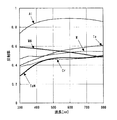
また、本発明において用いるレーザ光は基板を透過することが必須条件である。そこで、図6(A)に波長に対する1737ガラス基板の透過率を、図6(B)波長に対する合成石英ガラス基板の透過率を示す。図6より、用いる基板にある程度の透過率を必要とするのなら、前記レーザ光の波長は300nm以上(好ましくは400nm以上)が望ましい。また、図6より、用いるレーザによって、基板を選択することが望ましい。例えば、XeClエキシマレーザ(波長308nm)を用いるなら、1737ガラス基板より合成石英ガラス基板の方が透過率が高いため、合成石英ガラス基板を用いる方が望ましい。さらに、用いるレーザはガスレーザより固体レーザが望ましい。ガスレーザに用いるガスは一般に非常に高価であり、ガス交換の頻度が高くなると製造コストの増加を招くという問題がある。また、レーザ発振を行なうレーザチューブや発振過程で生成した不要な化合物を除去するためのガス精製器などの付属機器の交換が2〜3年に一度必要となる。これらの付属機器は高価なものが多く、やはり製造コストの増加を招くという問題がある。そのため、YAGレーザ等の固体レーザ(結晶ロッドを共振キャビティとしたレーザ光を出力するレーザ)を用いれば、ガスレーザに比べランニングコスト(ここでは稼働に伴い発生する費用を意味する)を低くすることができるためである。
【0034】
また、半導体膜基板に該半導体膜基板の表面側からレーザ光を照射する際、前記レーザ光を前記半導体膜基板に対して、斜めから照射しても良い。
【0035】
また、前記反射体は1度作製しておけば、何度でも利用することができる。
【0036】
また、半導体膜として非晶質半導体膜や結晶質半導体膜があり、非晶質珪素膜のほかに、非晶質珪素ゲルマニウム膜などの非晶質構造を有する化合物半導体膜を適用しても良い。
【0037】
以上のような本発明を適用することで、金属元素のゲッタリング、半導体膜の結晶性の回復および不純物元素の活性化が十分に行なわれた半導体膜を得ることができ、半導体装置の性能を大幅に向上させうる。例えば、TFTを例に挙げると、金属元素のゲッタリングが十分に行なわれることで、オフ電流値を低減させ、しかもオフ電流値のばらつきを抑えることを可能とする。また、半導体膜の結晶性の回復が十分に行なわれることで、チャネル形成領域が高抵抗領域となり、リーク電流を低下させることを可能とする。また、不純物元素の活性化が十分に行なわれることで、不純物元素が添加された領域を低抵抗領域にしてLDD領域、ソース領域およびドレイン領域として機能させることを可能とする。
【0038】
【発明の実施の形態】
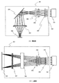
本発明の実施形態について説明する。図1(A)はレーザ照射装置の構成を示す図である。このレーザ照射装置は、レーザ発振器101、レーザ発振器101を発振源とするレーザ光210(高調波が望ましい。好ましくは第2高調波)を線状に加工する光学系201、透光性基板を固定するステージ102を有し、ステージ102にはヒータ103とヒータコントローラー104が具備されて、基板を450℃まで加熱することができる。また、ステージ102上には反射体105が設けられ、その上に半導体膜が形成された基板106が設置される。
【0039】
前記レーザ発振器101として、パルス発振型または連続発光型の固体レーザまたは気体レーザまたは金属レーザ等から射出されたレーザ光を用いることができる。なお、レーザ発振器101から出力されたレーザ光を第2高調波または第3高調波に変調する場合は、レーザ発振器101の直後に非線形素子を含む波長変調器を設ければ良い。
【0040】
次に、図1(A)のような構成のレーザ照射装置において、基板106の保持方法を図1(B)を用いて説明する。ステージ102に保持された基板106は、反応室107に設置され、レーザ101を発振源とする線状のレーザ光が照射される。反応室内は図示されていない排気系またはガス系により減圧状態または不活性ガス雰囲気とすることができ、半導体膜を汚染させることなく100〜450℃まで加熱することができる。
【0041】
また、ステージ102はガイドレール108に沿って反応室107内を移動することができ、基板の全面に線状のレーザ光を照射することができる。レーザ光は基板106の上面に設けられた図示されていない石英製の窓から入射する。また、図1(B)ではこの反応室107にトランスファー室109、中間室110、ロード・アンロード室111が接続され、それぞれの室は仕切弁112、113で分離されている。
【0042】
ロード・アンロード室111には複数の基板を保持することが可能なカセット114が設置され、トランスファー室109に設けられた搬送ロボット115により基板が搬送される。基板106'は搬送中の基板を表す。このような構成とすることによりレーザアニールを減圧下または不活性ガス雰囲気中で連続して処理することができる。
【0043】
次に、レーザ光を線状にする光学系201の構成について図2を用いて説明する。図2(A)は光学系201を側面から見た図であり、図2(B)は光学系201を上面から見た図である。
【0044】
レーザ101を発振源とするレーザ光はシリンドリカルアレイレンズ202により縦方向に分割される。この分割されたレーザ光はシリンドリカルレンズ203によりさらに横方向に分割される。即ち、レーザ光はシリンドリカルアレイレンズ202、203によって最終的にはマトリクス状に分割されることになる。
【0045】
そして、レーザ光はシリンドリカルレンズ204により一旦集光される。その際、シリンドリカルレンズ204の直後にシリンドリカルレンズ205を通る。その後、ミラー206で反射され、シリンドリカルレンズ207を通った後、照射面208に達する。
【0046】
このとき、照射面208に投影されたレーザ光は線状の照射面を示す。即ち、シリンドリカルレンズ207を透過したレーザ光の断面形状は線状になっていることを意味する。この線状に加工されたレーザ光の幅方向(短い方向)の均質化は、シリンドリカルアレイレンズ202、シリンドリカルレンズ204及びシリンドリカルレンズ207で行われる。また、上記レーザ光の長さ方向(長い方向)の均質化は、シリンドリカルアレイレンズ203及びシリンドリカルレンズ205で行われる。
【0047】
次に、基板上に形成された半導体膜を裏面側からレーザ光を照射するための構成について図3を用いて説明する。図3に示したのは、図1における基板106と反射体105との位置関係を示す図である。
【0048】
図3において、311はGOLD構造のTFTのゲート電極まで形成されているものである。また、311の下にはレーザ光を反射させるための反射体312が配置される。
【0049】
ここで、TFTのゲート電極まで形成する方法について図4を用いて説明する。まず、透光性基板300はガラス基板、合成石英ガラス基板、結晶化ガラス基板若しくはプラスチック基板が用いられる。下地絶縁膜301は公知の手段(スパッタ法、LPCVD法、またはプラズマCVD法等)により、酸化珪素膜や窒化酸化珪素膜(SiOxNy)などの珪素を含む絶縁膜を用いれば良い。もちろん他の絶縁膜を用いても良く、下地絶縁膜は単層でなく、積層としてもよい。
【0050】
そして、非晶質構造を有する半導体膜302を公知の手段(スパッタ法、LPCVD法、またはプラズマCVD法等)により、25〜80nm(好ましくは30〜60nm)の厚さで形成する。半導体膜の材料に限定はないが、好ましくは珪素または珪素ゲルマニウム(SiGe)合金などで形成するとよい。そして前記半導体膜に結晶化を助長する金属元素(Fe、Co、Ni、Ru、Rh、Pd、Os、Ir、Pt、Cu、Ag、Au、Sn、Sbから選ばれた一種または複数種)を添加して金属含有層303を形成し、加熱処理を行なって半導体膜を結晶化させる。もちろん、他の公知の結晶化法(レーザ結晶化法など)を組み合わせても良い。(図4(A))
【0051】
結晶化した半導体膜をパターニングして島状半導体膜304を形成した後、絶縁膜305を酸化珪素膜や窒化酸化珪素膜(SiOxNy)などの珪素を含む絶縁膜などで形成し、導電膜306を形成する。導電膜の材料に特に限定はないが、Ta、W、Ti、Mo、Al、Cu、Cr、Ndから選ばれた元素、または前記元素を主成分とする合金材料若しくは化合物材料で形成してもよい。また、リン等の不純物元素をドーピングした結晶質珪素膜に代表される半導体膜を用いてもよい。また、AgPdCu合金を用いてもよい。もちろん、導電膜は単層ではなく、積層としてもよい。続いてエッチングを行なって端部にテーパーを有するゲート電極307を形成する。
【0052】
そして、ドーピング処理を行なって、不純物元素の導入を行なう。ドーピング処理は、イオンドープ法やイオン注入法などにより、希ガス元素から選ばれた一種または複数種の元素と、n型を付与する不純物元素またはp型を付与する不純物元素を導入する。希ガス元素から選ばれた一種または複数種の元素、n型を付与する不純物元素およびp型を付与する不純物元素を導入してもよい。加えて、水素を添加してもよい。もちろん、希ガス元素を導入する工程と、n型を付与する不純物元素またはp型を付与する不純物元素を導入する工程とを分けて行なっても良い。ドーピング処理により、不純物元素が高濃度に導入された領域308、ゲート電極の端部のテーパーにより低濃度に導入された領域309および不純物元素が導入されない領域(チャネル形成領域)310が形成される。そして、加熱処理を行なって、前記金属元素のゲッタリングを行なう。前記加熱処理により、チャネル形成領域から不純物元素が添加された領域へ金属元素が移動し、チャネル形成領域を高抵抗領域とすることができる。
【0053】
そして、希ガス元素が導入された領域の結晶性の回復を十分に行なうための方法を図3に示す。
【0054】
ここで、反射体312は表面(レーザ光の反射面)に金属膜を形成した基板であっても良いし、反射率の高い材料で形成された反射板であっても良い。この場合、金属膜としては如何なる材料を用いても良い。代表的には、アルミニウム、銀、タングステン、チタン、タンタルのいずれかの元素を含む金属膜を用いる。
【0055】
また、反射体312を配置する代わりに、基板300の裏面(表面の反対側の面)に直接上述のような金属膜を形成し、そこでレーザ光を反射させることも可能である。但し、その構成は半導体装置の作製過程で裏面に形成した金属膜が除去されないことが前提である。
【0056】
そして、図2で説明した光学系201(図中ではシリンドリカルレンズ207のみを示す。)を経由して線状に加工されたレーザ光が、ゲート電極307の下方の半導体膜にも照射される。
【0057】
このとき、半導体膜に照射されるレーザ光には、シリンドリカルレンズ207を通過して直接照射されるレーザ光313と、反射体312で一旦反射されて半導体膜へ照射されるレーザ光314とがある。なお、本明細書中では、反射体の表面に照射されるレーザ光を第1のレーザ光と呼び、反射体によって反射されるレーザ光を第2のレーザ光と呼ぶ。
【0058】
シリンドリカルレンズ207を通過したレーザ光は、集光される過程で基板表面に対して45〜90°の入射角を持つ。そのため、第2のレーザ光314は半導体膜の裏面側にも回り込んで照射される。また、反射体312の反射面に起伏部を設けてレーザ光を乱反射させることで、第2のレーザ光314をさらに効率良く得ることができる。また、反射体312の反射面を曲面(例えば、凹面)にすれば、レーザ光を集光しながら半導体膜に照射することができ、効率が良い。
【0059】
以上のように、本発明によれば、固体レーザを発振源とするレーザ光を線状に加工することが可能であり、且つ、そのレーザ光を第1のレーザ光および第2のレーザ光に分光して、半導体膜の裏面に照射することが可能である。さらに、ソース領域およびドレイン領域はLDD領域に比べて低抵抗領域でなくてはならないが、第1のレーザ光および第2のレーザ光が照射されるため、不純物元素の活性化が十分行なわれることになる。
【0060】
さらに、レーザ照射装置のステージ102にはヒータ103とヒータコントローラー104が具備されているため、基板を100〜450℃まで加熱しながら、レーザ光を照射することが可能となり、さらに効率良く結晶性の回復および不純物元素の活性化を行なうことができる。
【0061】
また、図19に示すように、半導体膜基板に対してレーザ光を斜めから照射すれば、第2のレーザ光はゲート電極と重なる半導体膜により照射されやすくなり、前記半導体膜の結晶性の回復および不純物元素の活性化が十分に行なわれることになる。
【0062】
以上の構成でなる本発明について、以下に示す実施例でもってさらに詳細な説明を行なうこととする。
【0063】
【実施例】
[実施例1]
本発明の実施例について説明する。図1(A)はレーザ照射装置の構成を示す図である。このレーザ照射装置は、レーザ発振器101、レーザ発振器101を発振源とするレーザ光210(好ましくは第2高調波)を線状に加工する光学系201、透光性基板を固定するステージ102を有し、ステージ102にはヒータ103とヒータコントローラー104が具備されて、基板を100〜450℃まで加熱することができる。また、ステージ102上には反射体105が設けられ、その上に半導体膜が形成された基板106が設置される。
【0064】
なお、レーザ発振器101から出力されたレーザ光を第2高調波または第3高調波に変調する場合は、レーザ発振器101の直後に非線形素子を含む波長変調器を設ければ良い。本実施例ではレーザ発振器101として、Nd:YAGレーザを用い、非線形光学素子によって第2高調波に変調したレーザ光を用いた。しかしながら、Nd:YAGレーザはコヒーレント性の高いレーザであるため、光学系201の前に薄膜偏光素子(TFP:Thin Film Polarizer)および偏光板などを設置して、レーザ発振器101から発振されたレーザ光の一部に光路長を追加し、照射面における干渉を防ぐことが望ましい。
【0065】
次に、図1(A)のような構成のレーザ照射装置において、基板106の保持方法を図1(B)を用いて説明する。ステージ102に保持された基板106は、反応室107に設置され、レーザ101を発振源とする線状のレーザ光が照射される。反応室内は図示されていない排気系またはガス系により減圧状態または不活性ガス雰囲気とすることができ、半導体膜を汚染させることなく100〜450℃まで加熱することができる。
【0066】
また、ステージ102はガイドレール108に沿って反応室内を移動することができ、基板の全面に線状のレーザ光を照射することができる。レーザ光は基板106の上面に設けられた図示されていない石英製の窓から入射する。また、図1(B)ではこの反応室107にトランスファー室109、中間室110、ロード・アンロード室111が接続され、それぞれの室は仕切弁112、113で分離されている。
【0067】
ロード・アンロード室111には複数の基板を保持することが可能なカセット114が設置され、トランスファー室109に設けられた搬送ロボット115により基板が搬送される。基板106'は搬送中の基板を表す。このような構成とすることによりレーザアニールを減圧下または不活性ガス雰囲気中で連続して処理することができる。
【0068】
次に、レーザ光を線状にする光学系201の構成について図2を用いて説明する。図2(A)は光学系201を側面から見た図であり、図2(B)は光学系201を上面から見た図である。
【0069】
レーザ101を発振源とするレーザ光はシリンドリカルアレイレンズ202により縦方向に分割される。この分割されたレーザ光はシリンドリカルレンズ203によりさらに横方向に分割される。即ち、レーザ光はシリンドリカルアレイレンズ202、203によって最終的にはマトリクス状に分割されることになる。
【0070】
そして、レーザ光はシリンドリカルレンズ204により一旦集光される。その際、シリンドリカルレンズ204の直後にシリンドリカルレンズ205を通る。その後、ミラー206で反射され、シリンドリカルレンズ207を通った後、照射面208に達する。
【0071】
このとき、照射面208に投影されたレーザ光は線状の照射面を示す。即ち、シリンドリカルレンズ207を透過したレーザ光の断面形状は線状になっていることを意味する。この線状に加工されたレーザ光の幅方向(短い方向)の均質化は、シリンドリカルアレイレンズ202、シリンドリカルレンズ204及びシリンドリカルレンズ207で行われる。また、上記レーザ光の長さ方向(長い方向)の均質化は、シリンドリカルアレイレンズ203及びシリンドリカルレンズ205で行われる。
【0072】
次に、基板上に形成された半導体膜を裏面側からレーザ光を照射するための構成について図3を用いて説明する。図3に示したのは、図1における基板106と反射体105との位置関係を示す図である。
【0073】
図3において、311はTFTのゲート電極まで形成されているものである。また、311の下にはレーザ光を反射させるための反射体312が配置される。
【0074】
ここで、TFTのゲート電極まで形成する方法について図4を用いて説明する。まず、透光性基板300はガラス基板、合成石英ガラス基板、結晶化ガラス基板若しくはプラスチック基板が用いられる。本実施例では透光性基板として合成石英ガラス基板を用いる。
【0075】
そして、下地絶縁膜301は公知の手段(スパッタ法、LPCVD法、またはプラズマCVD法等)により、酸化珪素膜や窒化酸化珪素膜(SiOxNy)などの珪素を含む絶縁膜を用いれば良い。もちろん下地絶縁膜は単層でなく、積層としてもよい。本実施例では、プラズマCVD法により膜厚150nmの酸化珪素膜を形成する。
【0076】
そして、非晶質構造を有する半導体膜302を公知の手段(スパッタ法、LPCVD法、またはプラズマCVD法等)により、25〜200nm、好ましくは25〜80nm(代表的には30〜60nm)の厚さで形成する。半導体膜の材料に限定はないが、好ましくは珪素または珪素ゲルマニウム(SiGe)合金などで形成するとよい。本実施例では、プラズマCVD法により、膜厚50nmの非晶質珪素膜を形成する。そして前記半導体膜に結晶化を助長する金属元素を添加して金属含有層303を形成する。前記金属元素の導入する方法は、プラズマ処理や蒸着、スパッタ法、イオン注入、溶液塗布等を利用すればよい。本実施例では、酢酸ニッケル水溶液(重量換算濃度5ppm、体積5ml)を前記非晶質珪素膜表面にスピンコート法にて塗布する。そして、加熱処理を行なって半導体膜を結晶化させる。加熱時間や温度は、半導体膜や添加する金属元素によるので、実施者が適宜決定すれば良い。本実施例では、550℃の窒素雰囲気中に4時間曝す。結晶化した半導体膜のパターニングして島状半導体膜を形成した後、絶縁膜305を公知の手段(スパッタ法、LPCVD法、またはプラズマCVD法等)により、酸化珪素膜や窒化酸化珪素膜(SiOxNy)などの珪素を含む絶縁膜などで形成する。
【0077】
続いて、導電膜306を形成する。導電膜の材料に特に限定はないが、Ta、W、Ti、Mo、Al、Cu、Cr、Ndから選ばれた元素、または前記元素を主成分とする合金材料若しくは化合物材料で形成してもよい。また、リン等の不純物元素をドーピングした結晶質珪素膜に代表される半導体膜を用いてもよい。また、AgPdCu合金を用いてもよい。もちろん、導電膜は単層ではなく、積層としてもよい。本実施例では、膜厚400nmのW膜からなる導電膜306を形成する。W膜は、Wのターゲットを用いたスパッタ法で形成する。その他に6フッ化タングステン(WF6)を用いる熱CVD法で形成することもできる。
【0078】
続いてエッチングを行なって端部にテーパーを有するゲート電極307を形成する。フォトリソグラフィ法を用いてレジストからなるマスク(図示せず)を形成し、電極及び配線を形成するためのエッチング処理を行なう。本実施例ではエッチング処理として、ICP(Inductively Coupled Plasma:誘導結合型プラズマ)エッチング法を用い、エッチング用ガスにCF4とCl2とO2とを用い、それぞれのガス流量比を25:25:10(sccm)とし、1Paの圧力でコイル型の電極に500WのRF(13.56MHz)電力を投入してプラズマを生成してエッチングを行なった。ここでは、松下電器産業(株)製のICPを用いたドライエッチング装置(Model E645−□ICP)を用いた。基板側(試料ステージ)にも150WのRF(13.56MHz)電力を投入し、実質的に負の自己バイアス電圧を印加する。このエッチング処理によりW膜をエッチングして導電層の端部をテーパー形状とする。なお、ゲート絶縁膜上に残渣を残すことなくエッチングするためには、10〜20%程度の割合でエッチング時間を増加させると良い。上記エッチング処理では、レジストからなるマスクの形状を適したものとすることにより、基板側に印加するバイアス電圧の効果により導電層の端部がテーパー形状となる。このテーパー部の角度は15〜45°となる。304はゲート絶縁膜であり、導電層306で覆われない領域は20〜50nm程度エッチングされ薄くなった領域が形成される。
【0079】
そして、ドーピング処理を行なって、不純物元素の導入を行なう。ドーピング処理は、イオンドープ法やイオン注入法などにより、希ガス元素から選ばれた一種または複数種の元素と、n型を付与する不純物元素またはp型を付与する不純物元素を導入する。希ガス元素から選ばれた一種または複数種の元素、n型を付与する不純物元素およびp型を付与する不純物元素を導入してもよい。加えて、水素を添加してもよい。もちろん、希ガス元素を導入する工程と、n型を付与する不純物元素またはp型を付与する不純物元素を導入する工程とを分けて行なっても良い。ドーピング処理により、不純物元素が高濃度に導入された領域308、ゲート電極の端部のテーパーにより低濃度に導入された領域309および不純物元素が導入されない領域(チャネル形成領域)310が形成される。本実施例では、15族に属する元素としてリンを、希ガス元素としてアルゴンを用いた。リンの注入条件は、水素で希釈された5%のPH3を用い、加速電圧80keV、ドーズ量1.5×10¹⁵/cm2とした。注入に要する時間は約8分であり、結晶質半導体膜には平均濃度で2×1020/cm3のリンを注入することができる。一方、アルゴンは90keVの加速電圧で、2×1015/cm2のドーズ量で注入した。
【0080】
続いて、加熱処理を行なって、前記金属元素のゲッタリングを行なう。前記加熱処理により、チャネル形成領域から不純物元素が添加された領域へ金属元素が移動し、チャネル形成領域を高抵抗領域とすることができる。本実施例では、窒素雰囲気中、550℃にて4時間の加熱処理を行ってゲッタリングを行った。
【0081】
そして、希ガス元素が導入された領域の結晶性の回復を十分に行なうための方法を図3に示す。
【0082】
ここで、反射体312は表面(レーザ光の反射面)に金属膜を形成した基板であっても良いし、反射率の高い材料で形成された反射板であっても良い。この場合、金属膜としては如何なる材料を用いても良い。代表的には、アルミニウム、銀、タングステン、チタン、タンタルのいずれかの元素を含む金属膜を用いる。
【0083】
また、反射体312を配置する代わりに、基板300の裏面(表面の反対側の面)に直接上述のような金属膜を形成し、そこでレーザ光を反射させることも可能である。但し、その構成は半導体装置の作製過程で裏面に形成した金属膜が除去されないことが前提である。本実施例では、合成石英ガラス基板にアルミニウムをスパッタにより成膜したものを反射体として用いる。
【0084】
そして、図2で説明した光学系201(図中ではシリンドリカルレンズ207のみを示す。)を経由して線状に加工されたレーザ光が、ゲート電極307の下方の半導体膜にも照射される。
【0085】
このとき、半導体膜に照射されるレーザ光には、シリンドリカルレンズ207を通過して直接照射されるレーザ光313と、反射体312で一旦反射されて半導体膜へ照射されるレーザ光314とがある。なお、本明細書中では、反射体の表面に照射されるレーザ光を第1のレーザ光と呼び、反射体によって反射されるレーザ光を第2のレーザ光と呼ぶ。
【0086】
シリンドリカルレンズ207を通過したレーザ光は、集光される過程で基板表面に対して45〜90°の入射角を持つ。そのため、第2のレーザ光314は半導体膜の裏面側にも回り込んで照射される。また、反射体312の反射面に起伏部を設けてレーザ光を乱反射させることで、第2のレーザ光314をさらに効率良く得ることができる。また、反射体312の反射面を凹面にすれば、レーザ光を集光しながら半導体膜に照射することができ、効率が良い。
【0087】
以上のように、本実施例によれば、固体レーザを発振源とするレーザ光を線状に加工することが可能であり、且つ、そのレーザ光を第1のレーザ光および第2のレーザ光に分光して、半導体膜の裏面に照射することが可能である。さらに、ソース領域およびドレイン領域はLDD領域に比べて低抵抗領域でなくてはならないが、第1のレーザ光および第2のレーザ光が照射されるため、結晶性の回復および不純物元素を活性化が十分行なわれることになる。
【0088】
さらに、レーザ照射装置のステージ102にはヒータ103とヒータコントローラー104が具備されているため、基板を450℃程度まで加熱しながら、レーザ光を照射することが可能となり、さらに効率良く結晶性の回復および不純物元素の活性化を行なうことができる。
【0089】
[実施例2]
本実施例では、実施例1とは異なる作製工程を経た半導体膜基板にレーザアニールを行なう場合について説明する。
【0090】
ここで、TFTのゲート電極まで形成する方法について図7を用いて説明する。まず、実施例1にしたがって、図4(A)の状態を得る。なお、図7(A)は図4(A)と同じ状態を示している。
【0091】
そして、第1の加熱処理を行なって半導体膜を結晶化させる。加熱時間や温度は、半導体膜や添加する金属元素によるので、実施者が適宜決定すれば良い。本実施例では、550℃の窒素雰囲気中に4時間曝す。
【0092】
続いて、マスク755を形成して、第1のドーピング処理を行ない、半導体膜に選択的に不純物元素を導入する。ドーピング処理は、イオンドープ法やイオン注入法などにより、希ガス元素から選ばれた一種または複数種の元素と、n型を付与する不純物元素またはp型を付与する不純物元素を導入する。希ガス元素から選ばれた一種または複数種の元素、n型を付与する不純物元素およびp型を付与する不純物元素を導入してもよい。加えて、水素を添加してもよい。本実施例では、イオンドープ法により、まずアルゴンのみを90keVの加速電圧で、2×10¹⁵/cm2のドーズ量で注入する。
【0093】
そして、第2の加熱処理を行なって、結晶化を助長するために用いた金属元素を不純物元素が導入された領域756へ移動させる(ゲッタリング)。本実施例では、窒素雰囲気中、550℃にて4時間の加熱処理を行ってゲッタリングを行なう。(図7(B))
【0094】
金属元素がゲッタリングされた領域756をエッチングし、またマスクを除去して、半導体層757を形成する。そして、絶縁膜758を公知の手段(スパッタ法、LPCVD法、またはプラズマCVD法等)により、酸化珪素膜や窒化酸化珪素膜(SiOxNy)などの珪素を含む絶縁膜などで形成する。
【0095】
続いて、導電膜759を形成する。導電膜の材料に特に限定はないが、Ta、W、Ti、Mo、Al、Cu、Cr、Ndから選ばれた元素、または前記元素を主成分とする合金材料若しくは化合物材料で形成してもよい。また、リン等の不純物元素をドーピングした結晶質珪素膜に代表される半導体膜を用いてもよい。また、AgPdCu合金を用いてもよい。もちろん、導電膜は単層ではなく、積層としてもよい。本実施例では、膜厚400nmのW膜からなる導電膜759を形成した。W膜は、Wのターゲットを用いたスパッタ法で形成する。(図7(C))
【0096】
続いてエッチングを行なって端部にテーパーを有するゲート電極760を形成する。フォトリソグラフィ法を用いてレジストからなるマスク(図示せず)を形成し、電極及び配線を形成するためのエッチング処理を行なう。該エッチング処理では、レジストからなるマスクの形状を適したものとすることにより、基板側に印加するバイアス電圧の効果により導電層の端部がテーパー形状となる。このテーパー部の角度は15〜45°となる。758はゲート絶縁膜であり、導電層760で覆われない領域は20〜50nm程度エッチングされ薄くなった領域が形成される。
【0097】
そして、ドーピング処理を行なって不純物元素の導入を行なう。ドーピング処理は、イオンドープ法やイオン注入法などにより、n型を付与する不純物元素またはp型を付与する不純物元素を導入する。ドーピング処理により、不純物元素が高濃度に導入された領域761、ゲート電極の端部のテーパーにより低濃度に導入された領域762および不純物元素が導入されない領域(チャネル形成領域)763が形成される。本実施例では、15族に属する元素としてリンを用いた。リンの注入条件は、水素で希釈された5%のPH3を用い、加速電圧80keV、ドーズ量1.5×10¹⁵/cm2とした。注入に要する時間は約8分であり、結晶質半導体膜には平均濃度で2×1020/cm3のリンを注入することができる。
【0098】
そして、加熱処理を行なって、前記金属元素のゲッタリングを行なう。前記加熱処理により、チャネル形成領域から不純物元素が添加された領域へ金属元素が移動し、チャネル形成領域を高抵抗領域とすることができる。本実施例では、窒素雰囲気中、550℃にて4時間の加熱処理を行ってゲッタリングを行った。(図7(D))
【0099】
そして、実施例1で説明した図3に示す方法で、不純物元素が導入された領域の結晶性の回復および不純物元素の活性化を行なう。
【0100】
ここで、反射体312は表面(レーザ光の反射面)に金属膜を形成した基板であっても良いし、反射率の高い材料で形成された反射板であっても良い。この場合、金属膜としては如何なる材料を用いても良い。代表的には、アルミニウム、銀、タングステン、チタン、タンタルのいずれかの元素を含む金属膜を用いる。
【0101】
さらに、レーザ照射装置のステージ102にはヒータ103とヒータコントローラー104が具備されているため、基板を450℃程度まで加熱しながら、レーザ光を照射することが可能となり、さらに効率良く結晶性の回復および不純物元素の活性化を行なうことができる。
【0102】
[実施例3]
本実施例では、実施例1および実施例2とは異なる作製工程を経た半導体膜基板にレーザアニールを行なう場合について説明する。
【0103】
ここで、TFTのゲート電極まで形成する方法について図20を用いて説明する。まず、実施例1にしたがって、図4(A)の半導体膜302が形成された状態を得る。なお、図4(A)と対応する部分には図20(A)において同じ符号を用いている。
【0104】
そして、開口部を有する絶縁膜770を公知の手段(スパッタ法、LPCVD法、またはプラズマCVD法等)により、酸化珪素膜や窒化酸化珪素膜(SiOxNy)などの珪素を含む絶縁膜で形成した後、結晶化を助長する金属元素を添加して金属含有層771を形成する。前記金属元素の導入する方法は、プラズマ処理や蒸着、スパッタ法、イオン注入、溶液塗布等を利用すればよい。第1の加熱処理を行なって半導体膜を結晶化させる。加熱時間や温度は、半導体膜や添加する金属元素によるので、実施者が適宜決定すれば良い。本実施例では、550℃の窒素雰囲気中に4時間曝す。
【0105】
続いて、第1のドーピング処理を行ない、半導体膜に選択的に不純物元素を導入する。ドーピング処理は、イオンドープ法やイオン注入法などにより、希ガス元素から選ばれた一種または複数種の元素を導入する。または、希ガス元素から選ばれた一種または複数種の元素と、n型を付与する不純物元素またはp型を付与する不純物元素を導入してもよい。希ガス元素から選ばれた一種または複数種の元素、n型を付与する不純物元素およびp型を付与する不純物元素を導入してもよい。加えて、水素を添加してもよい。本実施例では、イオンドープ法により、まずアルゴンのみを90keVの加速電圧で、2×10¹⁵/cm2のドーズ量で注入する。
【0106】
そして、第2の加熱処理を行なって、結晶化を助長するために用いた金属元素を不純物元素が導入された領域772へ移動させる(ゲッタリング)。本実施例では、窒素雰囲気中、550℃にて4時間の加熱処理を行ってゲッタリングを行なう。(図20(B))
【0107】
絶縁膜770および半導体膜の一部エッチングして、半導体層773を形成する。そして、絶縁膜774aを公知の手段(スパッタ法、LPCVD法、またはプラズマCVD法等)により、酸化珪素膜や窒化酸化珪素膜(SiOxNy)などの珪素を含む絶縁膜などで形成する。
【0108】
続いて、導電膜775を形成する。導電膜の材料に特に限定はないが、Ta、W、Ti、Mo、Al、Cu、Cr、Ndから選ばれた元素、または前記元素を主成分とする合金材料若しくは化合物材料で形成してもよい。また、リン等の不純物元素をドーピングした結晶質珪素膜に代表される半導体膜を用いてもよい。また、AgPdCu合金を用いてもよい。もちろん、導電膜は単層ではなく、積層としてもよい。本実施例では、膜厚400nmのW膜からなる導電膜775を形成する。(図20(C))
【0109】
続いてエッチングを行なって端部にテーパーを有するゲート電極776を形成する。フォトリソグラフィ法を用いてレジストからなるマスク(図示せず)を形成し、電極及び配線を形成するためのエッチング処理を行なう。該エッチング処理では、レジストからなるマスクの形状を適したものとすることにより、基板側に印加するバイアス電圧の効果により導電層の端部がテーパー形状となる。このテーパー部の角度は15〜45°となる。774bはゲート絶縁膜であり、ゲート電極776で覆われない領域は20〜50nm程度エッチングされ薄くなった領域が形成される。
【0110】
そして、第2のドーピング処理を行なって不純物元素の導入を行なう。ドーピング処理は、イオンドープ法やイオン注入法などにより、n型を付与する不純物元素またはp型を付与する不純物元素を導入する。ドーピング処理により、不純物元素が高濃度に導入された領域777、ゲート電極の端部のテーパーにより低濃度に導入された領域778および不純物元素が導入されない領域(チャネル形成領域)779が形成される。本実施例では、n型を付与する不純物元素としてリンを用いた。リンの注入条件は、水素で希釈された5%のPH3を用い、加速電圧80keV、ドーズ量1.5×10¹⁵/cm2とした。注入に要する時間は約8分であり、結晶質半導体膜には平均濃度で2×1020/cm3のリンを注入することができる。(図20(D))
【0111】
そして、実施例1で説明した図3に示す方法で、不純物元素が導入された領域の結晶性の回復および不純物元素の活性化を行なう。
【0112】
ここで、反射体312は表面(レーザ光の反射面)に金属膜を形成した基板であっても良いし、反射率の高い材料で形成された反射板であっても良い。この場合、金属膜としては如何なる材料を用いても良い。代表的には、アルミニウム、銀、タングステン、チタン、タンタルのいずれかの元素を含む金属膜を用いる。
【0113】
さらに、レーザ照射装置のステージ102にはヒータ103とヒータコントローラー104が具備されているため、基板を100〜450℃まで加熱しながら、レーザ光を照射することが可能となり、さらに効率良く結晶性の回復および不純物元素の活性化を行なうことができる。
【0114】
[実施例4]
本実施例では、実施例1乃至3とは異なる作製工程を経た半導体膜基板にレーザアニールを行なう場合について説明する。
【0115】
まず、TFTのゲート電極まで形成する方法について図23を用いて説明する。透光性基板300はガラス基板、合成石英ガラス基板、結晶化ガラス基板若しくはプラスチック基板が用いられる。本実施例では透光性基板として合成石英ガラス基板を用いる。
【0116】
導電膜を形成し、エッチングを行なって所望の形状の導電膜780を形成する。導電膜の材料に特に限定はないが、Ta、W、Ti、Mo、Al、Cu、Cr、Ndから選ばれた元素、または前記元素を主成分とする合金材料若しくは化合物材料で形成してもよい。また、リン等の不純物元素をドーピングした結晶質珪素膜に代表される半導体膜を用いてもよい。また、AgPdCu合金を用いてもよい。もちろん、導電膜は単層ではなく、積層としてもよい。本実施例では、膜厚400nmのW膜からなる導電膜780を形成する。W膜は、Wのターゲットを用いたスパッタ法で形成する。その他に6フッ化タングステン(WF6)を用いる熱CVD法で形成することもできる。
【0117】
そして、絶縁膜781は公知の手段(スパッタ法、LPCVD法、またはプラズマCVD法等)により、酸化珪素膜や窒化酸化珪素膜(SiOxNy)などの珪素を含む絶縁膜を用いれば良い。もちろん絶縁膜は単層でなく、積層としてもよい。本実施例では、プラズマCVD法により膜厚150nmの酸化珪素膜を形成する。
【0118】
続いて、非晶質構造を有する半導体膜782を公知の手段(スパッタ法、LPCVD法、またはプラズマCVD法等)により、25〜200nm、好ましくは25〜80nm(は30〜60nm)の厚さで形成する。半導体膜の材料に限定はないが、好ましくは珪素または珪素ゲルマニウム(SiGe)合金などで形成するとよい。本実施例では、プラズマCVD法により、膜厚50nmの非晶質珪素膜を形成する。そして公知の結晶化法を行なって前記半導体膜を結晶化させる。本実施例では、酢酸ニッケル水溶液(重量換算濃度5ppm、体積5ml)を前記非晶質珪素膜表面にスピンコート法にて塗布して金属含有層783を形成した後、550℃の窒素雰囲気中に4時間曝す。加熱時間や温度は、半導体膜や添加する金属元素によるので、実施者が適宜決定すれば良い。(図23(A))
【0119】
続いて、マスク784を形成して、ドーピング処理を行ない、半導体膜に選択的に不純物元素を導入する。ドーピング処理は、イオンドープ法やイオン注入法などにより、希ガス元素から選ばれた一種または複数種の元素と、n型を付与する不純物元素またはp型を付与する不純物元素を導入する。希ガス元素から選ばれた一種または複数種の元素、n型を付与する不純物元素およびp型を付与する不純物元素を導入してもよい。加えて、水素を添加してもよい。本実施例では、n型を付与する不純物元素としてリンを、希ガス元素としてアルゴンを用いた。リンの注入条件は、水素で希釈された5%のPH3を用い、加速電圧80keV、ドーズ量1.5×10¹⁵/cm2とした。注入に要する時間は約8分であり、結晶質半導体膜には平均濃度で2×1020/cm3のリンを注入することができる。一方、アルゴンは90keVの加速電圧で、2×1015/cm2のドーズ量で注入する。
【0120】
本実施例のように、半導体膜を結晶化させるために金属元素を用いた場合は、加熱処理を行なって、前記金属元素のゲッタリングを行なうことが望ましい。前記加熱処理により、チャネル形成領域786から不純物元素が添加された領域785へ金属元素が移動し、チャネル形成領域786を高抵抗領域とすることができる。本実施例では、窒素雰囲気中、550℃にて4時間の加熱処理を行ってゲッタリングを行なう。(図23(B))
【0121】
そして、マスク784を除去し、また、活性領域となる半導体層787を形成した後(図23(C))、実施例1乃至3と同様に、希ガス元素が導入された領域の結晶性の回復を十分に行なうためにレーザアニールを行なう。(図23(D))
【0122】
ここで、反射体312は表面(レーザ光の反射面)に金属膜を形成した基板であっても良いし、反射率の高い材料で形成された反射板であっても良い。この場合、金属膜としては如何なる材料を用いても良い。代表的には、アルミニウム、銀、タングステン、チタン、タンタルのいずれかの元素を含む金属膜を用いる。
【0123】
そして、図2で説明した光学系201(図中ではシリンドリカルレンズ207のみを示す。)を経由して線状に加工されたレーザ光が、半導体膜を裏面からも照射する。このような照射方法を適用することで、導電層780は熱伝導性が高いため、レーザアニールによる熱が逃げやすい。そのため、基板の裏面側からも照射することで、レーザアニールを効果的に行なうことが可能となる。
【0124】
さらに、レーザ照射装置のステージ102にはヒータ103とヒータコントローラー104が具備されているため、基板を450℃程度まで加熱しながら、レーザ光を照射することが可能となり、さらに効率良く結晶性の回復および不純物元素の活性化を行なうことができる。
【0125】
[実施例5]
本実施例ではアクティブマトリクス基板の作製方法について図8〜図12を用いて説明する。
【0126】
まず、本実施例ではコーニング社の#7059ガラスや#1737ガラスなどに代表されるバリウムホウケイ酸ガラス、またはアルミノホウケイ酸ガラスなどのガラスからなる基板320を用いる。なお、基板320としては、石英基板や可撓性基板などを用いることができる。可撓性基板とは、PET、PES、PEN、アクリルなどからなるフィルム状の基板のことであり、可撓性基板を用いて半導体装置を作製すれば、軽量化が見込まれる。可撓性基板の表面、または表面および裏面にアルミ膜(AlON、AlN、AlOなど)、炭素膜(DLC(ダイヤモンドライクカーボン)など)、SiNなどのバリア層を単層または多層にして形成すれば、耐久性などが向上するので望ましい。また、本実施例の処理温度に耐えうる耐熱性が有するプラスチック基板を用いてもよい。
【0127】
次いで、基板320上に酸化珪素膜、窒化珪素膜または酸化窒化珪素膜などの絶縁膜から成る下地膜321を形成する。本実施例では下地膜321として2層構造を用いるが、前記絶縁膜の単層膜または2層以上積層させた構造を用いても良い。下地膜301の一層目としては、プラズマCVD法を用い、SiH4、NH3、及びN2Oを反応ガスとして成膜される酸化窒化珪素膜321aを10〜200nm(好ましくは50〜100nm)形成する。本実施例では、膜厚50nmの酸化窒化珪素膜321a(組成比Si=32%、O=27%、N=24%、H=17%)を形成した。次いで、下地膜301のニ層目としては、プラズマCVD法を用い、SiH4、及びN2Oを反応ガスとして成膜される酸化窒化珪素膜321bを50〜200nm(好ましくは100〜150nm)の厚さに積層形成する。本実施例では、膜厚100nmの酸化窒化珪素膜321b(組成比Si=32%、O=59%、N=7%、H=2%)を形成する。
【0128】
次いで、下地膜上に半導体膜322を形成する。半導体膜322は、非晶質構造を有する半導体膜を公知の手段(スパッタ法、LPCVD法、またはプラズマCVD法等)により、25〜200nm、好ましくは25〜80nm(代表的には30〜60nm)の厚さで形成する。半導体膜の材料に限定はないが、好ましくは珪素または珪素ゲルマニウム(SiGe)合金などで形成すると良い。続いて、ニッケルなどの触媒を用いて金属含有層323を形成し熱結晶化法を行なう。もちろん、ニッケルなどの触媒を用いた熱結晶化法と、他の公知の結晶化処理(レーザ結晶化法、熱結晶化法等)を組み合わせても良い。このような方法により得られた結晶質半導体膜を所望の形状にパターニングして、半導体層402〜406を形成する。本実施例では、プラズマCVD法を用い、55nmの非晶質珪素膜を成膜した後、ニッケルを含む溶液を非晶質珪素膜上に保持させる。この非晶質珪素膜に脱水素化(500℃、1時間)を行った後、加熱処理(550℃、4時間)を行ない、結晶質珪素膜を形成した。そして、この結晶質珪素膜をフォトリソグラフィ法を用いたパターニング処理によって、半導体層402〜406を形成する。
【0129】
また、半導体膜の結晶化にレーザ結晶化法も適用する場合には、パルス発振型または連続発光型の固体レーザまたは気体レーザまたは金属レーザ等を用いることができる。なお、前記固体レーザとしては連続発振またはパルス発振のYAGレーザ、YVO4レーザ、YLFレーザ、YAlO3レーザ、ガラスレーザ、ルビーレーザ、アレキサンドライドレーザ、Ti:サファイアレーザ等があり、前記気体レーザとしては連続発振またはパルス発振のエキシマレーザ、Arレーザ、Krレーザ、CO2レーザ等があり、前記金属レーザとしてはヘリウムカドミウムレーザ、銅蒸気レーザ、金蒸気レーザが挙げられる。これらのレーザを用いる場合には、レーザ発振器から放射されたレーザ光を光学系で線状に集光し半導体膜に照射する方法を用いると良い。結晶化の条件は実施者が適宣選択するものであるが、エキシマレーザを用いる場合はパルス発振周波数300Hzとし、レーザーエネルギー密度を100〜1200mJ/cm2、好ましくは100〜800mJ/cm2(代表的には200〜700mJ/cm2)とする。また、YAGレーザを用いる場合にはその第2高調波を用いパルス発振周波数1〜300Hzとし、レーザーエネルギー密度を300〜1500mJ/cm2、好ましくは300〜1000mJ/cm2(代表的には350〜800mJ/cm2)とすると良い。そして幅100〜1000μm、例えば400μmで線状に集光したレーザ光を基板全面に渡って照射し、この時の線状レーザ光の重ね合わせ率(オーバーラップ率)を50〜98%として行ってもよい。また連続発振のレーザを用いる場合のエネルギー密度は0.01〜100MW/cm2程度(好ましくは0.1〜10MW/cm2)が必要である。そして、0.5〜2000cm/s程度の速度でレーザ光に対して相対的にステージを動かして照射し、結晶性珪素膜を形成する。
【0130】
半導体層402〜406を形成した後、TFTのしきい値を制御するために微量な不純物元素(ボロンまたはリン)のドーピングを行なってもよい。
【0131】
次いで、半導体層402〜406を覆うゲート絶縁膜407を形成する。ゲート絶縁膜407はプラズマCVD法またはスパッタ法を用い、厚さを40〜150nmとして珪素を含む絶縁膜で形成する。本実施例では、プラズマCVD法により110nmの厚さで酸化窒化珪素膜(組成比Si=32%、O=59%、N=7%、H=2%)で形成した。もちろん、ゲート絶縁膜は酸化窒化珪素膜に限定されるものでなく、他の珪素を含む絶縁膜を単層または積層構造として用いても良い。
【0132】
また、酸化珪素膜を用いる場合には、プラズマCVD法でTEOS(Tetraethyl Orthosilicate)とO2とを混合し、反応圧力40Pa、基板温度300〜400℃とし、高周波(13.56MHz)電力密度0.5〜0.8W/cm2で放電させて形成することができる。このようにして作製される酸化珪素膜は、その後400〜500℃の熱アニールによりゲート絶縁膜として良好な特性を得ることができる。
【0133】
次いで、図8(B)に示すように、ゲート絶縁膜407上に膜厚20〜100nmの第1の導電膜408と、膜厚100〜400nmの第2の導電膜409とを積層形成する。本実施例では、膜厚30nmのTaN膜からなる第1の導電膜408と、膜厚370nmのW膜からなる第2の導電膜409を積層形成した。TaN膜はスパッタ法で形成し、Taのターゲットを用い、窒素を含む雰囲気内でスパッタした。また、W膜は、Wのターゲットを用いたスパッタ法で形成した。その他に6フッ化タングステン(WF6)を用いる熱CVD法で形成することもできる。いずれにしてもゲート電極として使用するためには低抵抗化を図る必要があり、W膜の抵抗率は20μΩcm以下にすることが望ましい。W膜は結晶粒を大きくすることで低抵抗率化を図ることができるが、W膜中に酸素などの不純物元素が多い場合には結晶化が阻害され高抵抗化する。従って、本実施例では、高純度のW(純度99.9999%)のターゲットを用いたスパッタ法で、さらに成膜時に気相中からの不純物の混入がないように十分配慮してW膜を形成することにより、抵抗率9〜20μΩcmを実現することができた。
【0134】
なお、本実施例では、第1の導電膜408をTaN、第2の導電膜409をWとしたが、特に限定されず、いずれもTa、W、Ti、Mo、Al、Cu、Cr、Ndから選ばれた元素、または前記元素を主成分とする合金材料若しくは化合物材料で形成してもよい。また、リン等の不純物元素をドーピングした結晶質珪素膜に代表される半導体膜を用いてもよい。また、AgPdCu合金を用いてもよい。また、第1の導電膜をタンタル(Ta)膜で形成し、第2の導電膜をW膜とする組み合わせ、第1の導電膜を窒化チタン(TiN)膜で形成し、第2の導電膜をW膜とする組み合わせ、第1の導電膜を窒化タンタル(TaN)膜で形成し、第2の導電膜をAl膜とする組み合わせ、第1の導電膜を窒化タンタル(TaN)膜で形成し、第2の導電膜をCu膜とする組み合わせとしてもよい。
【0135】
次に、フォトリソグラフィ法を用いてレジストからなるマスク410〜415を形成し、電極及び配線を形成するための第1のエッチング処理を行なう。第1のエッチング処理では第1及び第2のエッチング条件で行なう。本実施例では第1のエッチング条件として、ICP(Inductively Coupled Plasma:誘導結合型プラズマ)エッチング法を用い、エッチング用ガスにCF4とCl2とO2とを用い、それぞれのガス流量比を25:25:10(sccm)とし、1Paの圧力でコイル型の電極に500WのRF(13.56MHz)電力を投入してプラズマを生成してエッチングを行った。ここでは、松下電器産業(株)製のICPを用いたドライエッチング装置(Model E645−□ICP)を用いた。基板側(試料ステージ)にも150WのRF(13.56MHz)電力を投入し、実質的に負の自己バイアス電圧を印加する。この第1のエッチング条件によりW膜をエッチングして第1の導電層の端部をテーパー形状とする。
【0136】
この後、レジストからなるマスク410〜415を除去せずに第2のエッチング条件に変え、エッチング用ガスにCF4とCl2とを用い、それぞれのガス流量比を30:30(sccm)とし、1Paの圧力でコイル型の電極に500WのRF(13.56MHz)電力を投入してプラズマを生成して約30秒程度のエッチングを行った。基板側(試料ステージ)にも20WのRF(13.56MHz)電力を投入し、実質的に負の自己バイアス電圧を印加する。CF4とCl2を混合した第2のエッチング条件ではW膜及びTaN膜とも同程度にエッチングされる。なお、ゲート絶縁膜上に残渣を残すことなくエッチングするためには、10〜20%程度の割合でエッチング時間を増加させると良い。
【0137】
上記第1のエッチング処理では、レジストからなるマスクの形状を適したものとすることにより、基板側に印加するバイアス電圧の効果により第1の導電層及び第2の導電層の端部がテーパー形状となる。このテーパー部の角度は15〜45°となる。こうして、第1のエッチング処理により第1の導電層と第2の導電層から成る第1の形状の導電層417〜422(第1の導電層417a〜422aと第2の導電層417b〜422b)を形成する。416はゲート絶縁膜であり、第1の形状の導電層417〜422で覆われない領域は20〜50nm程度エッチングされ薄くなった領域が形成される。
【0138】
そして、レジストからなるマスクを除去せずに第1のドーピング処理を行い、半導体層にn型を付与する不純物元素および結晶化を助長するために用いた金属元素をゲッタリングするための希ガス元素を添加する。(図9(A))ドーピング処理はイオンドープ法、若しくはイオン注入法で行なえば良い。イオンドープ法の条件はドーズ量を1×10¹³〜5×10¹⁵/cm2とし、加速電圧を60〜100keVとして行なう。本実施例ではドーズ量を1.5×1015/cm2とし、加速電圧を80keVとして行った。n型を付与する不純物元素として15族に属する元素、典型的にはリン(P)または砒素(As)を用いるが、ここではリン(P)を用いた。また、希ガス元素としてアルゴンを用いた。この場合、導電層417〜421がn型を付与する不純物元素に対するマスクとなり、自己整合的に第1の高濃度不純物領域306〜310が形成される。第1の高濃度不純物領域306〜310には1×1020〜1×1021/cm3の濃度範囲でn型を付与する不純物元素を添加する。一方、アルゴンは90keVの加速電圧で、2×1015/cm2のドーズ量で注入した。
【0139】
次いで、レジストからなるマスクを除去せずに第2のエッチング処理を行なう。ここでは、エッチングガスにCF4とCl2とO2とを用い、W膜を選択的にエッチングする。この時、第2のエッチング処理により第2の導電層428b〜433bを形成する。一方、第1の導電層417a〜422aは、ほとんどエッチングされず(428a〜433a)、第2の形状の導電層428〜433を形成する。
【0140】
次いで、レジストからなるマスクを除去せずに、図9(B)に示すように、第2のドーピング処理を行なう。この場合、第1のドーピング処理よりもドーズ量を下げて、70〜120keVの高い加速電圧で、n型を付与する不純物元素を導入する。本実施例ではドーズ量を1.5×10¹⁴/cm2とし、加速電圧を90keVとして行なった。第2のドーピング処理は第2の形状の導電層428〜433をマスクとして用い、第2の導電層428b〜433bの下方における半導体層にも不純物元素が導入され、新たに第2の高濃度不純物領域423a〜427aおよび低濃度不純物領域423b〜427bが形成される。
【0141】
次いで、レジストからなるマスクを除去した後、新たにレジストからなるマスク434aおよび434bを形成して、図9(C)に示すように、第3のエッチング処理を行なう。エッチング用ガスにSF6およびCl2とを用い、ガス流量比を50:10(sccm)とし、1.3Paの圧力でコイル型の電極に500WのRF(13.56MHz)電力を投入してプラズマを生成し、約30秒のエッチング処理を行なう。基板側(資料ステージ)には10WのRF(13.56MHz)電力を投入し、実質的には不の自己バイアス電圧を印加する。こうして、前記大3のエッチング処理により、pチャネル型TFTおよび画素部のTFT(画素TFT)のTaN膜をエッチングして、第3の形状の導電層435〜438(435a〜438a、435b〜438b)を形成する。
【0142】
次いで、レジストからなるマスクを除去した後、第2の形状の導電層428、430および第2の形状の導電層435〜438をマスクとして用い、ゲート絶縁膜416を選択的に除去して絶縁層439〜444を形成する。(図10(A))
【0143】
次いで、新たにレジストからなるマスク445a〜445cを形成して第3のドーピング処理を行なう。この第3のドーピング処理により、pチャネル型TFTの活性層となる半導体層に前記一導電型とは逆の導電型を付与する不純物元素が添加された不純物領域446a〜446c、447a〜447cを形成する。第2の導電層435a、438aを不純物元素に対するマスクとして用い、p型を付与する不純物元素を添加して自己整合的に不純物領域を形成する。本実施例では、不純物領域446a〜446c、447a〜447cはジボラン(B2H6)を用いたイオンドープ法で形成する。(図10(B))この第3のドーピング処理の際には、nチャネル型TFTを形成する半導体層はレジストからなるマスク445a〜445cで覆われている。第1のドーピング処理及び第2のドーピング処理によって、不純物領域446、447にはそれぞれ異なる濃度でリンが添加されているが、そのいずれの領域においてもp型を付与する不純物元素の濃度を2×10²⁰〜2×10²¹/cm3となるようにドーピング処理することにより、pチャネル型TFTのソース領域およびドレイン領域として機能するために何ら問題は生じない。本実施例では、pチャネル型TFTの活性層となる半導体層の一部が露呈しているため、不純物元素(ボロン)を添加しやすい利点を有している。
【0144】
以上までの工程で、それぞれの半導体層に不純物領域が形成される。
【0145】
次いで、レジストからなるマスク445a〜445cを除去して第1の層間絶縁膜461を形成する。この第1の層間絶縁膜461としては、プラズマCVD法またはスパッタ法を用い、厚さを100〜200nmとして珪素を含む絶縁膜で形成する。本実施例では、プラズマCVD法により膜厚150nmの酸化窒化珪素膜を形成した。もちろん、第1の層間絶縁膜461は酸化窒化珪素膜に限定されるものでなく、他の珪素を含む絶縁膜を単層または積層構造として用いても良い。
【0146】
次いで、図10(C)に示すように、加熱処理を行なって、半導体層の結晶性の回復、それぞれの半導体層に添加された不純物元素の活性化を行なう。この加熱処理はファーネスアニール炉を用いる熱アニール法で行なう。熱アニール法としては、酸素濃度が1ppm以下、好ましくは0.1ppm以下の窒素雰囲気中で400〜700℃、代表的には500〜550℃で行なえばよく、本実施例では550℃、4時間の熱処理で活性化処理を行った。なお、熱アニール法の他に、レーザアニール法、またはラピッドサーマルアニール法(RTA法)を適用することができる。
【0147】
なお、本実施例では、上記活性化処理と同時に、結晶化の際に触媒として使用したニッケルが高濃度のリンを含む不純物領域423a、425a、426a、446a、447aを結晶化する。そのため、前記不純物領域に前記金属元素がゲッタリングされ、主にチャネル形成領域となる半導体層中のニッケル濃度が低減される。このようにして作製したチャネル形成領域を有するTFTはオフ電流値が下がり、結晶性が良いことから高い電界効果移動度が得られ、良好な特性を達成することができる。
【0148】
また、第1の層間絶縁膜を形成する前に加熱処理を行なっても良い。ただし、用いた配線材料が熱に弱い場合には、本実施例のように配線等を保護するため層間絶縁膜(珪素を主成分とする絶縁膜、例えば窒化珪素膜)を形成した後で加熱処理を行なうことが好ましい。
【0149】
希ガス元素が導入された領域の結晶性の回復および不純物元素の活性化を十分に行なうため、基板の表面側から照射したレーザ光を、基板の裏面側に設置した反射体340によって反射させることで、基板の裏面側からレーザ光を照射する。(図10(C))レーザ光として、パルス発振型または連続発光型の固体レーザまたは気体レーザまたは金属レーザ等から射出されたレーザ光を用いることができる。本実施例では反射体340として、アルミニウム板を用い、基板に対して斜めからレーザ光を照射する。このとき、同時にヒーター等を利用して、基板の裏面側から加熱処理も行なえば、第1層間膜に含有する水素により、水素化処理を行なうことができる。
【0150】
また、TFTのしきい値を制御するために微量な不純物元素(ボロンまたはリン)のドーピングを行なった場合は、裏面からのレーザ光の照射により、チャネル形成領域の結晶性の回復も十分行なわれることになる。
【0151】
レーザアニールを行なう工程で、同時に加熱処理を行なわない場合は、3〜100%の水素を含む雰囲気中で、300〜550℃で1〜12時間の熱処理を行ない、半導体層を水素化する工程を行なうことが望ましい。本実施例では水素を約3%の含む窒素雰囲気中で410℃、1時間の熱処理を行った。この工程は層間絶縁膜に含まれる水素により半導体層のダングリングボンドを終端する工程である。水素化の他の手段として、プラズマ水素化(プラズマにより励起された水素を用いる)を行なっても良い。
【0152】
次いで、第1の層間絶縁膜461上に無機絶縁膜材料または有機絶縁物材料から成る第2の層間絶縁膜462を形成する。本実施例では、膜厚1.6μmのアクリル樹脂膜を形成したが、粘度が10〜1000cp、好ましくは40〜200cpのものを用い、表面に凸凹が形成されるものを用いた。
【0153】
本実施例では、鏡面反射を防ぐため、表面に凸凹が形成される第2の層間絶縁膜462を形成することによって画素電極の表面に凸凹を形成した。また、画素電極の表面に凹凸を持たせて光散乱性を図るため、画素電極の下方の領域に凸部を形成してもよい。その場合、凸部の形成は、TFTの形成と同じフォトマスクで行なうことができるため、工程数の増加なく形成することができる。なお、この凸部は配線及びTFT部以外の画素部領域の基板上に適宜設ければよい。こうして、凸部を覆う絶縁膜の表面に形成された凸凹に沿って画素電極の表面に凸凹が形成される。
【0154】
また、第2の層間絶縁膜462として表面が平坦化する膜を用いてもよい。その場合は、画素電極を形成した後、公知のサンドブラスト法やエッチング法等の工程を追加して表面を凹凸化させて、鏡面反射を防ぎ、反射光を散乱させることによって白色度を増加させることが好ましい。
【0155】
そして、駆動回路506において、各不純物領域とそれぞれ電気的に接続する配線463〜467を形成する。なお、これらの配線は、膜厚50nmのTi膜と、膜厚500nmの合金膜(AlとTiとの合金膜)との積層膜をパターニングして形成する。
【0156】
また、画素部507においては、画素電極470、ゲート配線469、接続電極468を形成する。(図11)この接続電極468によりソース配線436(436aと436bの積層)は、画素TFTと電気的な接続が形成される。また、ゲート配線469は、画素TFTのゲート電極と電気的な接続が形成される。また、画素電極470は、画素TFTのドレイン領域426aと電気的な接続が形成され、さらに保持容量505を形成する一方の電極として機能する半導体層447a、447bと電気的な接続が形成される。また、画素電極470としては、AlまたはAgを主成分とする膜、またはそれらの積層膜等の反射性の優れた材料を用いることが望ましい。
【0157】
以上の様にして、nチャネル型TFT501とpチャネル型TFT502からなるCMOS回路508、及びnチャネル型TFT503を有する駆動回路506と、画素TFT504、保持容量505とを有する画素部507を同一基板上に形成することができる。こうして、アクティブマトリクス基板が完成する。
【0158】
駆動回路506のnチャネル型TFT501はチャネル形成領域423c、ゲート電極の一部を構成する第1の導電層428aと重なる低濃度不純物領域423b(GOLD領域)、とソース領域またはドレイン領域として機能する高濃度不純物領域423aを有している。このnチャネル型TFT501と電極466で接続してCMOS回路を形成するpチャネル型TFT502にはチャネル形成領域446d、ゲート電極の外側に形成される不純物領域446b、446c、ソース領域またはドレイン領域として機能する高濃度不純物領域446aを有している。また、nチャネル型TFT503にはチャネル形成領域425c、ゲート電極の一部を構成する第1の導電層430aと重なる低濃度不純物領域425b(GOLD領域)、とソース領域またはドレイン領域として機能する高濃度不純物領域425aを有している。
【0159】
画素部の画素TFT504にはチャネル形成領域426c、ゲート電極の外側に形成される低濃度不純物領域426b(LDD領域)とソース領域またはドレイン領域として機能する高濃度不純物領域426aを有している。また、保持容量505の一方の電極として機能する半導体層447a、447bには、それぞれp型を付与する不純物元素が添加されている。保持容量505は、絶縁膜444を誘電体として、電極(438aと438bの積層)と、半導体層447a〜447cとで形成している。
【0160】
また、本実施例の画素構造は、ブラックマトリクスを用いることなく、画素電極間の隙間が遮光されるように、画素電極の端部をソース配線と重なるように配置形成する。
【0161】
また、本実施例で作製するアクティブマトリクス基板の画素部の上面図を図12に示す。なお、図8〜図11に対応する部分には同じ符号を用いている。図11中の鎖線A−A’は図12中の鎖線A―A’で切断した断面図に対応している。また、図11中の鎖線B−B’は図12中の鎖線B―B’で切断した断面図に対応している。
【0162】
[実施例6]
本実施例では、実施例5で作製したアクティブマトリクス基板から、反射型液晶表示装置を作製する工程を以下に説明する。説明には図13を用いる。
【0163】
まず、実施例5に従い、図11の状態のアクティブマトリクス基板を得た後、図11のアクティブマトリクス基板上、少なくとも画素電極470上に配向膜567を形成しラビング処理を行なう。なお、本実施例では配向膜567を形成する前に、アクリル樹脂膜等の有機樹脂膜をパターニングすることによって基板間隔を保持するための柱状のスペーサ572を所望の位置に形成した。また、柱状のスペーサに代えて、球状のスペーサを基板全面に散布してもよい。
【0164】
次いで、対向基板569を用意する。次いで、対向基板569上に着色層570、571、平坦化膜573を形成する。赤色の着色層570と青色の着色層572とを重ねて、遮光部を形成する。また、赤色の着色層と緑色の着色層とを一部重ねて、遮光部を形成してもよい。
【0165】
本実施例では、実施例5に示す基板を用いている。従って、実施例5の画素部の上面図を示す図12では、少なくともゲート配線469と画素電極470の間隙と、ゲート配線469と接続電極468の間隙と、接続電極468と画素電極470の間隙を遮光する必要がある。本実施例では、それらの遮光すべき位置に着色層の積層からなる遮光部が重なるように各着色層を配置して、対向基板を貼り合わせた。
【0166】
このように、ブラックマスク等の遮光層を形成することなく、各画素間の隙間を着色層の積層からなる遮光部で遮光することによって工程数の低減を可能とした。
【0167】
次いで、平坦化膜573上に透明導電膜からなる対向電極576を少なくとも画素部に形成し、対向基板の全面に配向膜574を形成し、ラビング処理を施した。
【0168】
そして、画素部と駆動回路が形成されたアクティブマトリクス基板と対向基板とをシール材568で貼り合わせる。シール材568にはフィラーが混入されていて、このフィラーと柱状スペーサによって均一な間隔を持って2枚の基板が貼り合わせられる。その後、両基板の間に液晶材料575を注入し、封止剤(図示せず)によって完全に封止する。液晶材料575には公知の液晶材料を用いれば良い。このようにして図13に示す反射型液晶表示装置が完成する。そして、必要があれば、アクティブマトリクス基板または対向基板を所望の形状に分断する。さらに、対向基板のみに偏光板(図示しない)を貼りつけた。そして、公知の技術を用いてFPCを貼りつけた。
【0169】
以上のようにして作製される液晶表示パネルは各種電子機器の表示部として用いることができる。
【0170】
なお、本実施例は実施例1乃至5と自由に組み合わせることが可能である。
【0171】
[実施例7]
本実施例では、実施例5で作製したアクティブマトリクス基板から、実施例6とは異なるアクティブマトリクス型液晶表示装置を作製する工程を以下に説明する。説明には図21を用いる。
【0172】
まず、実施例5に従い、図11の状態のアクティブマトリクス基板を得た後、図11のアクティブマトリクス基板上に配向膜1067を形成しラビング処理を行なう。なお、本実施例では配向膜1067を形成する前に、アクリル樹脂膜等の有機樹脂膜をパターニングすることによって基板間隔を保持するための柱状のスペーサを所望の位置に形成した。また、柱状のスペーサに代えて、球状のスペーサを基板全面に散布してもよい。
【0173】
次いで、対向基板1068を用意する。この対向基板には、着色層1074、遮光層1075が各画素に対応して配置されたカラーフィルタが設けられている。また、駆動回路の部分にも遮光層1077を設けた。このカラーフィルタと遮光層1077とを覆う平坦化膜1076を設けた。次いで、平坦化膜176上に透明導電膜からなる対向電極1069を画素部に形成し、対向基板の全面に配向膜1070を形成し、ラビング処理を施した。
【0174】
そして、画素部と駆動回路が形成されたアクティブマトリクス基板と対向基板とをシール材1071で貼り合わせる。シール材1071にはフィラーが混入されていて、このフィラーと柱状スペーサによって均一な間隔を持って2枚の基板が貼り合わせられる。その後、両基板の間に液晶材料1073を注入し、封止剤(図示せず)によって完全に封止する。液晶材料1073には公知の液晶材料を用いれば良い。このようにして図21に示すアクティブマトリクス型液晶表示装置が完成する。そして、必要があれば、アクティブマトリクス基板または対向基板を所望の形状に分断する。さらに、公知の技術を用いて偏光板等を適宜設けた。そして、公知の技術を用いてFPCを貼りつけた。
【0175】
以上のようにして作製される液晶表示パネルは各種電子機器の表示部として用いることができる。
【0176】
なお、本実施例は実施例1乃至5と自由に組み合わせることが可能である。
【0177】
[実施例8]
本実施例では、本発明を用いて発光装置を作製した例について説明する。本明細書において、発光装置とは、基板上に形成された発光素子を該基板とカバー材の間に封入した表示用パネルおよび該表示用パネルにICを実装した表示用モジュールを総称したものである。なお、発光素子は、電場を加えることで発生するルミネッセンス(Electro Luminescence)が得られる有機化合物を含む層(発光層)と陽極層と、陰極層とを有する。また、有機化合物におけるルミネッセンスには、一重項励起状態から基底状態に戻る際の発光(蛍光)と三重項励起状態から基底状態に戻る際の発光(リン光)があり、これらのうちどちらか、あるいは両方の発光を含む。
【0178】
なお、本明細書中では、発光素子において陽極と陰極の間に形成された全ての層を有機発光層と定義する。有機発光層には具体的に、発光層、正孔注入層、電子注入層、正孔輸送層、電子輸送層等が含まれる。基本的に発光素子は、陽極層、発光層、陰極層が順に積層された構造を有しており、この構造に加えて、陽極層、正孔注入層、発光層、陰極層や、陽極層、正孔注入層、発光層、電子輸送層、陰極層等の順に積層した構造を有していることもある。
【0179】
図14は本実施例の発光装置の断面図である。図14において、基板700上に設けられた画素部612のスイッチングTFT603は図11のnチャネル型TFT503を用いて形成される。したがって、構造の説明はnチャネル型TFT503の説明を参照すれば良い。
【0180】
なお、本実施例ではチャネル形成領域が二つ形成されるダブルゲート構造としているが、チャネル形成領域が一つ形成されるシングルゲート構造もしくは三つ形成されるトリプルゲート構造であっても良い。
【0181】
基板700上に設けられた駆動回路610は図11のCMOS回路508を用いて形成される。従って、構造の説明はnチャネル型TFT501とpチャネル型TFT502の説明を参照すれば良い。なお、本実施例ではシングルゲート構造としているが、ダブルゲート構造もしくはトリプルゲート構造であっても良い。
【0182】
また、配線701、703はCMOS回路のソース配線、702はドレイン配線として機能する。また、配線704はソース配線708とスイッチングTFTのソース領域とを電気的に接続する配線として機能し、配線705はドレイン配線709とスイッチングTFTのドレイン領域とを電気的に接続する配線として機能する。
【0183】
なお、電流制御TFT604は図11のpチャネル型TFT502を用いて形成される。従って、構造の説明はpチャネル型TFT502の説明を参照すれば良い。なお、本実施例ではシングルゲート構造としているが、ダブルゲート構造もしくはトリプルゲート構造であっても良い。
【0184】
また、配線706は電流制御TFT604のソース配線(電流供給線に相当する)であり、707は電流制御TFT604の画素電極710上に重ねることで画素電極710と電気的に接続する電極である。
【0185】
なお、710は、透明導電膜からなる画素電極(発光素子の陽極)である。透明導電膜としては、酸化インジウムと酸化スズとの化合物、酸化インジウムと酸化亜鉛との化合物、酸化亜鉛、酸化スズまたは酸化インジウムを用いることができる。また、前記透明導電膜にガリウムを添加したものを用いても良い。画素電極710は、上記配線を形成する前に平坦な層間絶縁膜711上に形成する。本実施例においては、樹脂からなる平坦化膜711を用いてTFTによる段差を平坦化することは非常に重要である。後に形成される発光層は非常に薄いため、段差が存在することによって発光不良を起こす場合がある。従って、発光層をできるだけ平坦面に形成しうるように画素電極を形成する前に平坦化しておくことが望ましい。
【0186】
配線701〜707を形成後、図14に示すようにバンク712を形成する。バンク712は100〜400nmの珪素を含む絶縁膜もしくは有機樹脂膜をパターニングして形成すれば良い。
【0187】
なお、バンク712は絶縁膜であるため、成膜時における素子の静電破壊には注意が必要である。本実施例ではバンク712の材料となる絶縁膜中にカーボン粒子や金属粒子を添加して抵抗率を下げ、静電気の発生を抑制する。この際、抵抗率は1×10⁶〜1×10¹²Ωm(好ましくは1×10⁸〜1×10¹⁰Ωm)となるようにカーボン粒子や金属粒子の添加量を調節すれば良い。
【0188】
画素電極710の上には発光層713が形成される。なお、図14では一画素しか図示していないが、本実施例ではR(赤)、G(緑)、B(青)の各色に対応した発光層を作り分けている。また、本実施例では蒸着法により低分子系有機発光材料を形成している。具体的には、正孔注入層として20nm厚の銅フタロシアニン(CuPc)膜を設け、その上に発光層として70nm厚のトリス−8−キノリノラトアルミニウム錯体(Alq3)膜を設けた積層構造としている。Alq3にキナクリドン、ペリレンもしくはDCM1といった蛍光色素を添加することで発光色を制御することができる。
【0189】
但し、以上の例は発光層として用いることのできる有機発光材料の一例であって、これに限定する必要はまったくない。発光層、電荷輸送層または電荷注入層を自由に組み合わせて発光層(発光及びそのためのキャリアの移動を行なわせるための層)を形成すれば良い。例えば、本実施例では低分子系有機発光材料を発光層として用いる例を示したが、中分子系有機発光材料や高分子系有機発光材料を用いても良い。なお、本明細書中において、昇華性を有さず、かつ、分子数が20以下または連鎖する分子の長さが10μm以下の有機発光材料を中分子系有機発光材料とする。また、高分子系有機発光材料を用いる例として、正孔注入層として20nmのポリチオフェン(PEDOT)膜をスピン塗布法により設け、その上に発光層として100nm程度のパラフェニレンビニレン(PPV)膜を設けた積層構造としても良い。なお、PPVのπ共役系高分子を用いると、赤色から青色まで発光波長を選択できる。また、電荷輸送層や電荷注入層として炭化珪素等の無機材料を用いることも可能である。これらの有機発光材料や無機材料は公知の材料を用いることができる。
【0190】
次に、発光層713の上には導電膜からなる陰極714が設けられる。本実施例の場合、導電膜としてアルミニウムとリチウムとの合金膜を用いる。勿論、公知のMgAg膜(マグネシウムと銀との合金膜)を用いても良い。陰極材料としては、周期表の1族もしくは2族に属する元素からなる導電膜もしくはそれらの元素を添加した導電膜を用いれば良い。
【0191】
この陰極714まで形成された時点で発光素子715が完成する。なお、ここでいう発光素子715は、画素電極(陽極)710、発光層713及び陰極714で形成されたダイオードを指す。
【0192】
発光素子715を完全に覆うようにしてパッシベーション膜716を設けることは有効である。パッシベーション膜716としては、炭素膜、窒化珪素膜もしくは窒化酸化珪素膜を含む絶縁膜からなり、該絶縁膜を単層もしくは組み合わせた積層で用いる。
【0193】
この際、カバレッジの良い膜をパッシベーション膜として用いることが好ましく、炭素膜、特にDLC(ダイヤモンドライクカーボン)膜を用いることは有効である。DLC膜は室温から100℃以下の温度範囲で成膜可能であるため、耐熱性の低い発光層713の上方にも容易に成膜することができる。また、DLC膜は酸素に対するブロッキング効果が高く、発光層713の酸化を抑制することが可能である。そのため、この後に続く封止工程を行なう間に発光層713が酸化するといった問題を防止できる。
【0194】
さらに、パッシベーション膜716上に封止材717を設け、カバー材718を貼り合わせる。封止材717としては紫外線硬化樹脂を用いれば良く、内部に吸湿効果を有する物質もしくは酸化防止効果を有する物質を設けることは有効である。また、本実施例においてカバー材718はガラス基板や石英基板やプラスチック基板(プラスチックフィルムも含む)の両面に炭素膜(好ましくはダイヤモンドライクカーボン膜)を形成したものを用いる。
【0195】
こうして図14に示すような構造の発光装置が完成する。なお、バンク712を形成した後、パッシベーション膜716を形成するまでの工程をマルチチャンバー方式(またはインライン方式)の成膜装置を用いて、大気解放せずに連続的に処理することは有効である。また、さらに発展させてカバー材718を貼り合わせる工程までを大気解放せずに連続的に処理することも可能である。
【0196】
こうして、基板700上にnチャネル型TFT601、602、スイッチングTFT(nチャネル型TFT)603および電流制御TFT(nチャネル型TFT)604が形成される。ここまでの製造工程で必要としたマスク数は、一般的なアクティブマトリクス型発光装置よりも少ない。
【0197】
即ち、TFTの製造工程が大幅に簡略化されており、歩留まりの向上および製造コストの低減が実現できる。
【0198】
さらに、図14を用いて説明したように、ゲート電極に絶縁膜を介して重なる不純物領域を設けることによりホットキャリア効果に起因する劣化に強いnチャネル型TFTを形成することができる。そのため、信頼性の高い発光装置を実現できる。
【0199】
また、本実施例では画素部と駆動回路の構成のみ示しているが、本実施例の製造工程に従えば、その他にも信号分割回路、D/Aコンバータ、オペアンプ、γ補正回路などの論理回路を同一の絶縁体上に形成可能であり、さらにはメモリやマイクロプロセッサをも形成しうる。
【0200】
さらに、発光素子を保護するための封止(または封入)工程まで行った後の本実施例の発光装置について図15を用いて説明する。なお、必要に応じて図14で用いた符号を引用する。
【0201】
図15(A)は、発光素子の封止までを行った状態を示す上面図、図15(B)は図15(A)をC−C’で切断した断面図である。点線で示された801はソース側駆動回路、806は画素部、807はゲート側駆動回路である。また、901はカバー材、902は第1シール材、903は第2シール材であり、第1シール材902で囲まれた内側には封止材907が設けられる。
【0202】
なお、904はソース側駆動回路801及びゲート側駆動回路807に入力される信号を伝送するための配線であり、外部入力端子となるFPC(フレキシブルプリントサーキット)905からビデオ信号やクロック信号を受け取る。なお、ここではFPCしか図示されていないが、このFPCにはプリント配線基盤(PWB)が取り付けられていても良い。本明細書における発光装置には、発光装置本体だけでなく、それにFPCもしくはPWBが取り付けられた状態をも含むものとする。
【0203】
次に、断面構造について図15(B)を用いて説明する。基板700の上方には画素部806、ゲート側駆動回路807が形成されており、画素部806は電流制御TFT604とそのドレインに電気的に接続された画素電極710を含む複数の画素により形成される。また、ゲート側駆動回路807はnチャネル型TFT601とpチャネル型TFT602とを組み合わせたCMOS回路(図14参照)を用いて形成される。
【0204】
画素電極710は発光素子の陽極として機能する。また、画素電極710の両端にはバンク712が形成され、画素電極710上には発光層713および発光素子の陰極714が形成される。
【0205】
陰極714は全画素に共通の配線としても機能し、接続配線904を経由してFPC905に電気的に接続されている。さらに、画素部806及びゲート側駆動回路807に含まれる素子は全て陰極714およびパッシベーション膜716で覆われている。
【0206】
また、第1シール材902によりカバー材901が貼り合わされている。なお、カバー材901と発光素子との間隔を確保するために樹脂膜からなるスペーサを設けても良い。そして、第1シール材902の内側には封止材907が充填されている。なお、第1シール材902、封止材907としてはエポキシ系樹脂を用いるのが好ましい。また、第1シール材902はできるだけ水分や酸素を透過しない材料であることが望ましい。さらに、封止材907の内部に吸湿効果をもつ物質や酸化防止効果をもつ物質を含有させても良い。
【0207】
発光素子を覆うようにして設けられた封止材907はカバー材901を接着するための接着剤としても機能する。また、本実施例ではカバー材901を構成する材料としてFRP(Fiberglass-Reinforced Plastics)、PVF(ポリビニルフロライド)、マイラー、ポリエステルまたはアクリルを用いることができる。
【0208】
また、封止材907を用いてカバー材901を接着した後、封止材907の側面(露呈面)を覆うように第2シール材903を設ける。第2シール材903は第1シール材902と同じ材料を用いることができる。
【0209】
以上のような構造で発光素子を封止材907に封入することにより、発光素子を外部から完全に遮断することができ、外部から水分や酸素等の発光層の酸化による劣化を促す物質が侵入することを防ぐことができる。従って、信頼性の高い発光装置が得られる。
【0210】
なお、本実施例は実施例1乃至5と自由に組み合わせることが可能である。
【0211】
[実施例9]
本実施例では、実施例8とは異なる画素構造を有した発光装置について説明する。説明には図22を用いる。
【0212】
図22では電流制御用TFT4501として図11のnチャネル型TFT504と同一構造のTFTを用いる。勿論、電流制御用TFT4501のゲート電極はスイッチング用TFT4402のドレイン配線に電気的に接続されている。また、電流制御用TFT4501のドレイン配線は画素電極4504に電気的に接続されている。
【0213】
本実施例では、導電膜からなる画素電極4504が発光素子の陰極として機能する。具体的には、アルミニウムとリチウムとの合金膜を用いるが、周期表の1族もしくは2族に属する元素からなる導電膜もしくはそれらの元素を添加した導電膜を用いれば良い。
【0214】
画素電極4504の上には発光層4505が形成される。なお、図22では一画素しか図示していないが、本実施例ではG(緑)に対応した発光層を蒸着法及び塗布法(好ましくはスピンコーティング法)により形成している。具体的には、電子注入層として20nm厚のフッ化リチウム(LiF)膜を設け、その上に発光層として70nm厚のPPV(ポリパラフェニレンビニレン)膜を設けた積層構造としている。
【0215】
次に、発光層4505の上には透明導電膜からなる陽極4506が設けられる。本実施例の場合、透明導電膜として酸化インジウムと酸化スズとの化合物もしくは酸化インジウムと酸化亜鉛との化合物からなる導電膜を用いる。
【0216】
この陽極4506まで形成された時点で発光素子4507が完成する。なお、ここでいう発光素子4507は、画素電極(陰極)4504、発光層4505及び陽極4506で形成されたダイオードを指す。
【0217】
発光素子4507を完全に覆うようにしてパッシベーション膜4508を設けることは有効である。パッシベーション膜4508としては、炭素膜、窒化珪素膜もしくは窒化酸化珪素膜を含む絶縁膜からなり、該絶縁膜を単層もしくは組み合わせた積層で用いる。
【0218】
さらに、パッシベーション膜4508上に封止材4509を設け、カバー材4510を貼り合わせる。封止材4509としては紫外線硬化樹脂を用いれば良く、内部に吸湿効果を有する物質もしくは酸化防止効果を有する物質を設けることは有効である。また、本実施例においてカバー材4510はガラス基板や石英基板やプラスチック基板(プラスチックフィルムも含む)の両面に炭素膜(好ましくはダイヤモンドライクカーボン膜)を形成したものを用いる。
【0219】
なお、本実施例は実施例1乃至5と自由に組み合わせることが可能である。
【0220】
[実施例10]
本発明を適用して、本願発明を実施して形成されたCMOS回路や画素部は様々な電気光学装置(アクティブマトリクス型液晶ディスプレイ、アクティブマトリクス型ECディスプレイ、アクティブマトリクス型発光ディスプレイ)に用いることが出来る。即ち、それら電気光学装置を表示部に組み込んだ電子機器全てに本発明を実施出来る。
【0221】
その様な電子機器としては、ビデオカメラ、デジタルカメラ、プロジェクター、ヘッドマウントディスプレイ(ゴーグル型ディスプレイ)、カーナビゲーション、カーステレオ、パーソナルコンピュータ、携帯情報端末(モバイルコンピュータ、携帯電話または電子書籍等)などが挙げられる。それらの一例を図16、図17及び図18に示す。
【0222】
図16(A)はパーソナルコンピュータであり、本体3001、画像入力部3002、表示部3003、キーボード3004等を含む。本発明を表示部3003に適用することができる。
【0223】
図16(B)はビデオカメラであり、本体3101、表示部3102、音声入力部3103、操作スイッチ3104、バッテリー3105、受像部3106等を含む。本発明を表示部3102に適用することができる。
【0224】
図16(C)はモバイルコンピュータ(モービルコンピュータ)であり、本体3201、カメラ部3202、受像部3203、操作スイッチ3204、表示部3205等を含む。本発明は表示部3205に適用できる。
【0225】
図16(D)はゴーグル型ディスプレイであり、本体3301、表示部3302、アーム部3303等を含む。本発明は表示部3302に適用することができる。
【0226】
図16(E)はプログラムを記録した記録媒体(以下、記録媒体と呼ぶ)を用いるプレーヤーであり、本体3401、表示部3402、スピーカ部3403、記録媒体3404、操作スイッチ3405等を含む。なお、このプレーヤーは記録媒体としてDVD(Digtial Versatile Disc)、CD等を用い、音楽鑑賞や映画鑑賞やゲームやインターネットを行なうことができる。本発明は表示部3402に適用することができる。
【0227】
図16(F)はデジタルカメラであり、本体3501、表示部3502、接眼部3503、操作スイッチ3504、受像部(図示しない)等を含む。本発明を表示部3502に適用することができる。
【0228】
図17(A)はフロント型プロジェクターであり、投射装置3601、スクリーン3602等を含む。本発明は投射装置3601の一部を構成する液晶表示装置3808やその他の駆動回路に適用することができる。
【0229】
図17(B)はリア型プロジェクターであり、本体3701、投射装置3702、ミラー3703、スクリーン3704等を含む。本発明は投射装置2702の一部を構成する液晶表示装置3808やその他の駆動回路に適用することができる。
【0230】
なお、図17(C)は、図17(A)及び図17(B)中における投射装置3601、3702の構造の一例を示した図である。投射装置3601、3702は、光源光学系3801、ミラー3802、3804〜3806、ダイクロイックミラー3803、プリズム3807、液晶表示装置3808、位相差板3809、投射光学系3810で構成される。投射光学系2810は、投射レンズを含む光学系で構成される。本実施例は三板式の例を示したが、特に限定されず、例えば単板式であってもよい。また、図17(C)中において矢印で示した光路に実施者が適宜、光学レンズや、偏光機能を有するフィルムや、位相差を調節するためのフィルム、IRフィルム等の光学系を設けてもよい。
【0231】
また、図17(D)は、図17(C)中における光源光学系3801の構造の一例を示した図である。本実施例では、光源光学系3801は、リフレクター2811、光源3812、レンズアレイ3813、3814、偏光変換素子2815、集光レンズ3816で構成される。なお、図17(D)に示した光源光学系は一例であって特に限定されない。例えば、光源光学系に実施者が適宜、光学レンズや、偏光機能を有するフィルムや、位相差を調節するフィルム、IRフィルム等の光学系を設けてもよい。
【0232】
ただし、図17に示したプロジェクターにおいては、透過型の電気光学装置を用いた場合を示しており、反射型の電気光学装置及び発光装置での適用例は図示していない。
【0233】
図18(A)は携帯電話であり、本体3901、音声出力部3902、音声入力部3903、表示部3904、操作スイッチ3905、アンテナ3906等を含む。本発明を表示部3904に適用することができる。
【0234】
図18(B)は携帯書籍(電子書籍)であり、本体4001、表示部4002、4003、記憶媒体4004、操作スイッチ4005、アンテナ4006等を含む。本発明は表示部4002、4003に適用することができる。
【0235】
図18(C)はディスプレイであり、本体4101、支持台4102、表示部4103等を含む。本発明は表示部4103に適用することができる。本発明のディスプレイは特に大画面化した場合において有利であり、対角10インチ以上(特に30インチ以上)のディスプレイには有利である。
【0236】
以上の様に、本発明の適用範囲は極めて広く、あらゆる分野の電子機器に適用することが可能である。また、本実施例の電子機器は実施例1〜9のどのような組み合わせからなる構成を用いても実現することができる。
【発明の効果】
本発明の構成を採用することにより、以下に示すような基本的有意性を得ることが出来る。
(a)従来のTFTの作製プロセスに完全に適合した、簡単な構成である。
(b)不純物元素の導入量を低減することができる。そのため、ゲート絶縁膜や半導体膜やその界面においてドーピング処理によるダメージを低減することができる。
(c)不純物元素が導入された半導体膜の結晶性の回復を容易なものする。
(d)不純物元素の活性化を十分行なうことができる。
(e)結晶化を助長するために用いた金属元素を十分に除去することができる。
(f)ゲート電極と低濃度不純物領域のオーバーラップ領域の幅を小さくする事ができる。そのことにより、トランジスタのさらなる微細化を可能とする。
(g)以上の利点を満たした上で、電気的特性の優れたTFTを作製できる方法である。
【図面の簡単な説明】
【図1】 本発明のレーザ装置の構成を示す図。
【図2】 本発明のレーザ装置の光学系の構成を示す図。
【図3】 本発明のレーザアニール方法の一例を示す図。
【図4】 本発明のGOLD構造のTFTの作製工程を示す図。
【図5】 本発明において用いる反射材料の例における波長に対する反射率を示す図。
【図6】 (A)1737ガラス基板における波長に対する透過率を示す図。
(B)合成石英ガラス基板における波長に対する透過率を示す図。
【図7】 GOLD構造のTFTの作製工程を示す図。
【図8】 画素TFT、駆動回路のTFTの作製工程の例を示す断面図。
【図9】 画素TFT、駆動回路のTFTの作製工程の例を示す断面図。
【図10】 画素TFT、駆動回路のTFTの作製工程の例を示す断面図。
【図11】 画素TFT、駆動回路のTFTの作製工程の例を示す断面図。
【図12】 画素部の画素を示す上面図。
【図13】 アクティブマトリクス型液晶表示装置の作製工程を示す断面図。
【図14】 発光装置の駆動回路及び画素部の断面構造図。
【図15】 (A)発光装置の上面図。
(B)発光装置の駆動回路及び画素部の断面構造図。
【図16】 半導体装置の例を示す図。
【図17】 半導体装置の例を示す図。
【図18】 半導体装置の例を示す図。
【図19】 本発明のレーザアニール方法の一例を示す図。
【図20】 GOLD構造のTFTの作製工程を示す図。
【図21】 アクティブマトリクス型液晶表示装置の作製工程を示す断面図。
【図22】 発光装置の画素部の断面構造図。
【図23】 TFTの作製工程および本発明のレーザアニールの一例を示す図。[0001]
BACKGROUND OF THE INVENTION
The present invention relates to a semiconductor device manufactured by including annealing of a semiconductor film using laser light (hereinafter referred to as laser annealing) in a process and a manufacturing method thereof. Note that the semiconductor device here includes an electro-optical device such as a liquid crystal display device and a light-emitting device and an electronic device including the electro-optical device as a component.
[0002]
[Prior art]
A technique for crystallizing or improving crystallinity by subjecting a semiconductor film formed on an insulating substrate such as glass to laser annealing has been widely studied. Silicon is often used for the semiconductor film.
[0003]
In recent years, there has been a remarkable movement to increase the area of a substrate for improving mass production efficiency, and a newly constructed mass production factory line is becoming standard with a substrate size of 600 mm × 720 mm. It is difficult to process a synthetic quartz glass substrate on such a large area substrate with the current technology, and even if it can be done, it will not decrease to the price that can be established as an industry. An example of a material capable of easily manufacturing a large-area substrate is a glass substrate. A glass substrate is less expensive than a synthetic quartz glass substrate that has been often used in the past, and has an advantage that a large-area substrate can be easily manufactured. In addition, the reason why lasers are used favorably for crystallization is that the melting point of the glass substrate is low. The laser can give high energy only to the semiconductor film without increasing the temperature of the substrate so much.
[0004]
One glass substrate is called Corning 7059, for example. Corning 7059 is very inexpensive, has good workability, and is easy to increase in area. However, Corning 7059 has a strain point temperature of 593 ° C., and there is a problem with heating at 600 ° C. or higher. One glass substrate is Corning 1737, which has a relatively high strain point temperature. Corning 1737 has a strain point temperature of 667 ° C., which is higher than the strain point temperature of Corning 7059. Even when an amorphous semiconductor film was formed on the Corning 1737 substrate and placed in an atmosphere at 600 ° C. for 20 hours, the substrate was not deformed so as to affect the manufacturing process. However, the heating time of 20 hours is too long for a mass production process, and the heating temperature of 600 ° C. is preferably as low as possible from the viewpoint of cost.
[0005]
In order to solve such problems, a new crystallization method has been devised. Details of the method are described in JP-A-7-183540. Here, the method will be briefly described. First, a trace amount of a metal element such as nickel, palladium, or lead is added to the amorphous semiconductor film. As the addition method, a plasma treatment method, a vapor deposition method, an ion implantation method, a sputtering method, a solution coating method, or the like may be used. After the addition, for example, when an amorphous semiconductor film is placed in a nitrogen atmosphere at 550 ° C. for 4 hours, a crystalline semiconductor film with good characteristics can be obtained. The optimal heating temperature, heating time, etc. for crystallization depend on the amount of the metal element added and the state of the amorphous semiconductor film.
[0006]
However, the technique has a problem that the metal element used for promoting crystallization remains in a high resistance layer (channel formation region or offset region). Since the metal element easily flows electricity, the resistance of the region that should be the high resistance layer is lowered. As a result, the off-current increases, and the stability and reliability of the TFT characteristics, such as variations among individual elements, are impaired.
[0007]
In order to solve this problem, a technique (gettering technique) for removing a metal element for promoting crystallization from a crystalline semiconductor film has been developed and disclosed in Japanese Patent Laid-Open No. 10-270363. In the gettering technique, first, an element belonging to Group 15 is selectively added to the crystalline semiconductor film and heat treatment is performed. By the heat treatment, the metal element in the region to which the element belonging to Group 15 is not added (gettering region) is released from the gettering region, diffuses, and is added to the region to which the element belonging to Group 15 is added ( Gettering area). As a result, the metal element can be removed or reduced in the gettering region, and the heating temperature at the time of gettering can be 600 ° C. or less that the glass substrate can withstand. It has also been confirmed that metal elements can be gettered by introducing not only elements belonging to Group 15 but also elements belonging to Group 13.
[0008]
Since the crystalline semiconductor film formed through such a manufacturing process has high mobility, a thin film transistor (TFT) is formed using the crystalline semiconductor film, for example, in an active matrix type electro-optical device or the like. It is actively used.
[0009]
Active matrix liquid crystal display devices include pixel circuits that display images for each functional block, and drive circuits for controlling pixel circuits such as shift register circuits, level shifter circuits, buffer circuits, and sampling circuits based on CMOS circuits. Are formed on a single substrate.
[0010]
In a pixel circuit of an active matrix liquid crystal display device, a TFT (pixel TFT) is disposed in each of tens to millions of pixels, and a pixel electrode is provided in each of the pixel TFTs. A counter electrode is provided on the counter substrate side with the liquid crystal interposed therebetween, and a kind of capacitor using the liquid crystal as a dielectric is formed. Then, the voltage applied to each pixel is controlled by the switching function of the TFT, and the liquid crystal is driven by controlling the charge to this capacitor, and the transmitted light quantity is controlled to display an image.
[0011]
The pixel TFT is composed of an n-channel TFT, and is driven by applying a voltage to the liquid crystal as a switching element. Since the liquid crystal is driven by alternating current, a method called frame inversion driving is often employed. In this method, in order to keep power consumption low, it is important that the characteristics required for the pixel TFT have a sufficiently low off-current value (drain current that flows when the TFT is off).
[0012]
As a TFT structure for reducing the off-current value, a lightly doped drain (LDD) structure is known. In this structure, a region to which an impurity element is added at a low concentration is provided between a channel formation region and a source region or a drain region formed by adding an impurity element at a high concentration, and this region is referred to as an LDD region. I'm calling. A so-called GOLD (Gate-drain Overlapped LDD) structure in which an LDD region is disposed so as to overlap with a gate electrode through a gate insulating film is known as means for preventing deterioration of an on-current value due to hot carriers. . With such a structure, it is known that a high electric field in the vicinity of the drain is relaxed, hot carrier injection is prevented, and the deterioration phenomenon is effective.
[0013]
In order to form the GOLD structure, the end portion of the gate electrode has a tapered shape. By adopting such a shape, a step of introducing an impurity element imparting n-type into the semiconductor layer forming the n-channel TFT, and an impurity element imparting p-type to the semiconductor layer forming the p-channel TFT are formed. In the introduction step, a source region and a drain region are formed in a portion that does not overlap with the gate electrode in one doping process, and an LDD region having a concentration gradient along the taper shape is formed below the taper of the gate electrode. Can be formed.
[0014]
In addition, in the doping process, the energy of ions implanted into the semiconductor film is much larger than the binding energy of the elements forming the semiconductor film. For this reason, ions implanted into the semiconductor film blow off elements forming the semiconductor film from lattice points to cause defects in the crystal. Therefore, heat treatment is often performed after the doping treatment in order to recover the defects and to activate the implanted impurity element at the same time. Examples of the heat treatment include a thermal annealing method using a furnace annealing furnace, a laser annealing method, and a rapid thermal annealing method (RTA method). In addition, activating the impurity element is an important process for making the region to which the impurity element is added a low-resistance region and functioning as an LDD region, a source region, and a drain region.
[0015]
[Problems to be solved by the invention]
Elements belonging to Group 15 are ion-doped (PH Three This is a method in which ions are dissociated by plasma and ions are accelerated by an electric field and injected into the semiconductor film. Basically, ions are not separated by mass). For example, when phosphorus is introduced, the required phosphorus concentration is 1 × 10 20 /cm Three That's it. Addition of an element belonging to Group 15 by ion doping causes amorphousness of the semiconductor film, but an increase in the concentration of the element belonging to Group 15 is a problem because it hinders recrystallization by subsequent heat treatment. . In addition, the addition of a high-concentration Group 15 element is problematic because it increases the processing time required for doping and reduces the throughput in the doping process.
[0016]
Further, an element belonging to Group 15 is an impurity element imparting n-type, and p required for reversing the conductivity type of an element belonging to Group 15 added to the source region and drain region of the p-channel TFT. The concentration of the impurity element that imparts the type (for example, an element belonging to Group 13) needs to be 1.5 to 3 times, and as the recrystallization becomes difficult, the resistance of the source region and the drain region is increased. It is a problem.
[0017]
The present invention is a technique for solving such a problem, effectively removing the metal element remaining in the crystalline semiconductor film obtained by using a metal element that promotes crystallization of the semiconductor film, and In a semiconductor device typified by an active matrix liquid crystal display device manufactured using a TFT by sufficiently recovering the crystallinity of the semiconductor film and activating the impurity element, the operating characteristics and reliability of the semiconductor device are improved. The goal is to realize improvements.
[0018]
[Means for Solving the Problems]
In the present invention, a substrate on which a semiconductor film is formed (hereinafter referred to as a semiconductor film substrate) in order to recover the crystallinity of a low-concentration impurity region overlapping with a part of a gate electrode and to activate an impurity element. On the back side (defined in this specification as the surface opposite to the surface on which the film is formed), a reflective plate (hereinafter referred to as a reflective plate) formed of a substrate on which a reflective film is formed or a highly reflective material , These are referred to as reflectors), and the semiconductor film is irradiated with laser light from the surface side of the semiconductor film substrate (in this specification, defined as a surface on which a film is formed). The laser light transmitted through the substrate is reflected by the reflector, and the laser light is irradiated again from the back side of the semiconductor film substrate. At this time, the substrate may be heated to about 450 ° C. By heating the substrate simultaneously with the laser light irradiation, the crystallinity of the semiconductor film can be recovered and the impurity element can be activated.
[0019]
As the laser light, laser light emitted from a pulse oscillation type or continuous light emission type solid laser, a gas laser, a metal laser, or the like can be used. The solid-state laser may be a continuous wave or pulsed YAG laser, YVO Four Laser, YLF laser, YAlO Three There are lasers, glass lasers, ruby lasers, alexandride lasers, Ti: sapphire lasers, etc., and the gas lasers are continuous wave or pulsed excimer lasers, Ar lasers, Kr lasers, CO 2 Examples of the metal laser include a helium cadmium laser, a copper vapor laser, and a gold vapor laser.
[0020]
The low concentration impurity region is a region into which an impurity of one conductivity type is introduced. As the one conductivity type impurity, an element belonging to Group 15 or an element belonging to Group 13 is applied. In addition, hydrogen may be added to the low-concentration impurity region, and the low-concentration impurity region includes both one-conductivity type impurities and hydrogen.
[0021]
The low-concentration impurity region may be doped with an element belonging to Group 15 and an element belonging to Group 13. The impurity region includes both an element belonging to Group 15 and an element belonging to Group 13.
[0022]
The low-concentration impurity region may be doped with an element belonging to Group 15, an element belonging to Group 13, and hydrogen, and the impurity region may contain an element belonging to Group 15, an element belonging to Group 13, and hydrogen. Both are included.
[0023]
Further, the present invention provides a semiconductor film that is crystallized using a metal element that promotes crystallization, an impurity region to which a rare gas element (also referred to as a rare gas) is added, and the semiconductor film is formed in the impurity region by heat treatment. Next, gettering is performed by segregating the metal element contained in the substrate, and subsequently, a reflector is installed on the back surface side of the semiconductor film substrate, and laser light is irradiated from the front surface side of the semiconductor film substrate. The laser light is irradiated from the back side.
[0024]
By using the rare gas element, the amount of impurity elements introduced can be reduced. Therefore, damage at the gate insulating film and the semiconductor film and their interface due to the doping process can be reduced, and the number of trap centers can be reduced. This can improve the reliability when a TFT is manufactured. In addition, since the number of trap centers is reduced, the width of the overlap region between the gate electrode and the low-concentration impurity region can be reduced. As a result, the transistor can be further miniaturized.
[0025]
The rare gas element is one or a plurality selected from He, Ne, Ar, Kr, and Xe, and these ions are accelerated by an electric field and injected into the semiconductor film to form dangling bonds and lattice distortion. Thus, a gettering site can be formed.
[0026]
In addition, one conductivity type impurity may be added to the impurity region to which the rare gas element is added, and the impurity region includes both the rare gas element and the one conductivity type impurity. As the one conductivity type impurity, an element belonging to Group 15 or an element belonging to Group 13 is applied. In addition, hydrogen may be added to the impurity region, and the impurity region contains both a rare gas element, one conductivity type impurity, and hydrogen.
[0027]
Further, an element belonging to Group 15 and an element belonging to Group 13 may be added to the impurity region to which the rare gas element is added, and the impurity region belongs to the rare gas element, the element belonging to Group 15 and the Group 13 Both elements are included.
[0028]
Further, an element belonging to Group 15 or an element belonging to Group 13 and hydrogen may be added to the impurity region to which the rare gas element is added, and the impurity region may be added to the rare gas element, the element belonging to Group 15 or the Group 13. Both the element to which it belongs and hydrogen are included.
[0029]
The semiconductor film substrate and the reflector may be placed in contact with each other or may be placed apart from each other.
[0030]
In addition, as a material for forming the reflector, a heat-resistant material is used, and a material having a high reflectance with respect to the laser beam is used. As shown in FIG. 5, an element selected from aluminum (Al), tungsten (W), tantalum (Ta), titanium (Ti), chromium (Cr) and silver (Ag), or a compound containing the element as a component Or you may form from an alloy. As the reflector, a reflective film may be formed on the substrate, or a reflective plate made of a material having high reflectance may be used.
[0031]
In the reflector, the surface on which the laser light is reflected may be a flat surface or a curved surface. The laser beam is focused on or near the surface of the semiconductor film formed on the substrate. Further, a part of the laser light passes through the substrate, is reflected by a reflector, and is irradiated from the back side of the semiconductor film. At this time, if the shape of the surface on which the laser light is reflected in the reflector is a flat surface, the laser light reflected by the reflector may spread more than the laser light incident from the surface side of the semiconductor film. Therefore, if the shape of the surface on which the laser beam is reflected in the reflector is a curved surface, the laser beam reflected and condensed by the reflector can be irradiated from the back side of the semiconductor film, The effective energy density for the semiconductor film can be further increased. Since the curvature of the curved surface varies depending on the state of the laser beam, the distance between the substrate and the reflector, etc., the practitioner may determine as appropriate. Further, an uneven portion may be provided on the reflecting surface of the reflector to diffusely reflect the laser beam.
[0032]
Further, when the substrate on which the semiconductor film is formed is irradiated with laser light from the surface side of the substrate, the substrate and the reflector may move relative to the laser light, or only the substrate may be You may move relatively with respect to a laser beam and the said reflector.
[0033]
Further, it is an essential condition that the laser light used in the present invention is transmitted through the substrate. FIG. 6A shows the transmittance of the 1737 glass substrate with respect to the wavelength, and FIG. 6B shows the transmittance of the synthetic quartz glass substrate with respect to the wavelength. From FIG. 6, if the substrate to be used requires a certain degree of transmittance, the wavelength of the laser beam is desirably 300 nm or more (preferably 400 nm or more). From FIG. 6, it is desirable to select the substrate depending on the laser to be used. For example, if a XeCl excimer laser (
[0034]
In addition, when the semiconductor film substrate is irradiated with laser light from the surface side of the semiconductor film substrate, the laser light may be irradiated obliquely onto the semiconductor film substrate.
[0035]
Moreover, if the said reflector is produced once, it can be utilized any number of times.
[0036]
Further, there are an amorphous semiconductor film and a crystalline semiconductor film as the semiconductor film, and in addition to the amorphous silicon film, a compound semiconductor film having an amorphous structure such as an amorphous silicon germanium film may be applied. .
[0037]
By applying the present invention as described above, a semiconductor film in which gettering of a metal element, recovery of crystallinity of a semiconductor film, and activation of an impurity element are sufficiently performed can be obtained, and the performance of a semiconductor device can be improved. Can greatly improve. For example, when a TFT is taken as an example, the gettering of a metal element is sufficiently performed, so that an off-current value can be reduced and variation in an off-current value can be suppressed. In addition, when the crystallinity of the semiconductor film is sufficiently restored, the channel formation region becomes a high resistance region, and leakage current can be reduced. In addition, when the impurity element is sufficiently activated, the region to which the impurity element is added can be made to function as an LDD region, a source region, and a drain region by using a low resistance region.
[0038]
DETAILED DESCRIPTION OF THE INVENTION
An embodiment of the present invention will be described. FIG. 1A illustrates a structure of a laser irradiation apparatus. In this laser irradiation apparatus, a
[0039]
As the
[0040]
Next, a method for holding the
[0041]
Further, the
[0042]
A
[0043]
Next, the configuration of the
[0044]
Laser light using the
[0045]
The laser light is once condensed by the
[0046]
At this time, the laser light projected on the
[0047]
Next, a structure for irradiating the semiconductor film formed on the substrate with laser light from the back side will be described with reference to FIG. FIG. 3 shows the positional relationship between the
[0048]
In FIG. 3,
[0049]
Here, a method for forming the gate electrode of the TFT will be described with reference to FIGS. First, the
[0050]
Then, a
[0051]
After the crystallized semiconductor film is patterned to form the island-shaped
[0052]
Then, an impurity element is introduced by performing a doping process. In the doping treatment, one or more elements selected from rare gas elements and an impurity element imparting n-type or an impurity element imparting p-type are introduced by an ion doping method, an ion implantation method, or the like. One or more elements selected from rare gas elements, an impurity element imparting n-type conductivity, and an impurity element imparting p-type conductivity may be introduced. In addition, hydrogen may be added. Needless to say, the step of introducing a rare gas element and the step of introducing an impurity element imparting n-type conductivity or an impurity element imparting p-type conductivity may be performed separately. By the doping process, a
[0053]
FIG. 3 shows a method for sufficiently recovering the crystallinity of the region where the rare gas element is introduced.
[0054]
Here, the
[0055]
Further, instead of disposing the
[0056]
Then, the laser light processed into a linear shape via the
[0057]
At this time, the laser light applied to the semiconductor film includes
[0058]
The laser beam that has passed through the
[0059]
As described above, according to the present invention, laser light using a solid laser as an oscillation source can be processed into a linear shape, and the laser light is converted into a first laser light and a second laser light. It is possible to split and irradiate the back surface of the semiconductor film. Further, the source region and the drain region must be low resistance regions as compared with the LDD region. However, since the first laser beam and the second laser beam are irradiated, the impurity element is sufficiently activated. become.
[0060]
Further, since the
[0061]
As shown in FIG. 19, when the semiconductor film substrate is irradiated with laser light from an oblique direction, the second laser light is easily irradiated by the semiconductor film overlapping the gate electrode, and the crystallinity of the semiconductor film is recovered. In addition, the impurity elements are sufficiently activated.
[0062]
The present invention having the above-described configuration will be described in more detail with the following embodiments.
[0063]
【Example】
[Example 1]
Examples of the present invention will be described. FIG. 1A illustrates a structure of a laser irradiation apparatus. This laser irradiation apparatus has a
[0064]
Note that when the laser light output from the
[0065]
Next, a method for holding the
[0066]
Further, the
[0067]
A
[0068]
Next, the configuration of the
[0069]
Laser light using the
[0070]
The laser light is once condensed by the
[0071]
At this time, the laser light projected on the
[0072]
Next, a structure for irradiating the semiconductor film formed on the substrate with laser light from the back side will be described with reference to FIG. FIG. 3 shows the positional relationship between the
[0073]
In FIG. 3, 311 is formed up to the gate electrode of the TFT. A
[0074]
Here, a method for forming the gate electrode of the TFT will be described with reference to FIGS. First, the
[0075]
As the
[0076]
Then, the
[0077]
Subsequently, a
[0078]
Subsequently, etching is performed to form a
[0079]
Then, an impurity element is introduced by performing a doping process. In the doping treatment, one or more elements selected from rare gas elements and an impurity element imparting n-type or an impurity element imparting p-type are introduced by an ion doping method, an ion implantation method, or the like. One or more elements selected from rare gas elements, an impurity element imparting n-type conductivity, and an impurity element imparting p-type conductivity may be introduced. In addition, hydrogen may be added. Needless to say, the step of introducing a rare gas element and the step of introducing an impurity element imparting n-type conductivity or an impurity element imparting p-type conductivity may be performed separately. By the doping process, a
[0080]
Subsequently, heat treatment is performed to getter the metal element. By the heat treatment, the metal element moves from the channel formation region to the region to which the impurity element is added, so that the channel formation region can be a high resistance region. In this example, gettering was performed by performing heat treatment at 550 ° C. for 4 hours in a nitrogen atmosphere.
[0081]
FIG. 3 shows a method for sufficiently recovering the crystallinity of the region where the rare gas element is introduced.
[0082]
Here, the
[0083]
Further, instead of disposing the
[0084]
Then, the laser light processed into a linear shape via the
[0085]
At this time, the laser light applied to the semiconductor film includes
[0086]
The laser beam that has passed through the
[0087]
As described above, according to the present embodiment, it is possible to process a laser beam having a solid laser as an oscillation source into a linear shape, and the laser beam is converted into a first laser beam and a second laser beam. And the back surface of the semiconductor film can be irradiated. Further, the source region and the drain region must be low resistance regions compared to the LDD region, but since the first laser beam and the second laser beam are irradiated, the crystallinity is restored and the impurity element is activated. Will be carried out sufficiently.
[0088]
Furthermore, since the
[0089]
[Example 2]
In this embodiment, a case where laser annealing is performed on a semiconductor film substrate that has undergone a manufacturing process different from that in
[0090]
Here, a method for forming the gate electrode of the TFT will be described with reference to FIG. First, according to the first embodiment, the state of FIG. Note that FIG. 7A shows the same state as FIG.
[0091]
Then, a first heat treatment is performed to crystallize the semiconductor film. Since the heating time and temperature depend on the semiconductor film and the metal element to be added, the practitioner may determine appropriately. In this example, the substrate is exposed to a nitrogen atmosphere at 550 ° C. for 4 hours.
[0092]
Subsequently, a
[0093]
Then, second heat treatment is performed to move the metal element used for promoting crystallization to the
[0094]
The
[0095]
Subsequently, a
[0096]
Subsequently, etching is performed to form a
[0097]
Then, an impurity element is introduced by performing a doping process. In the doping treatment, an impurity element imparting n-type conductivity or an impurity element imparting p-type conductivity is introduced by an ion doping method, an ion implantation method, or the like. By the doping process, a
[0098]
Then, heat treatment is performed to getter the metal element. By the heat treatment, the metal element moves from the channel formation region to the region to which the impurity element is added, so that the channel formation region can be a high resistance region. In this example, gettering was performed by performing heat treatment at 550 ° C. for 4 hours in a nitrogen atmosphere. (Fig. 7 (D))
[0099]
Then, by the method shown in FIG. 3 described in
[0100]
Here, the
[0101]
Furthermore, since the
[0102]
[Example 3]
In this embodiment, a case where laser annealing is performed on a semiconductor film substrate that has undergone a manufacturing process different from those in
[0103]
Here, a method for forming the gate electrode of the TFT will be described with reference to FIGS. First, according to
[0104]
After the insulating
[0105]
Subsequently, a first doping process is performed to selectively introduce an impurity element into the semiconductor film. In the doping process, one or more elements selected from rare gas elements are introduced by an ion doping method, an ion implantation method, or the like. Alternatively, one or more elements selected from rare gas elements and an impurity element imparting n-type conductivity or an impurity element imparting p-type conductivity may be introduced. One or more elements selected from rare gas elements, an impurity element imparting n-type conductivity, and an impurity element imparting p-type conductivity may be introduced. In addition, hydrogen may be added. In this embodiment, by ion doping, only argon is first accelerated at an acceleration voltage of 90 keV to 2 × 10 2. 15 /cm 2 Inject at a dose of.
[0106]
Then, second heat treatment is performed to move the metal element used for promoting crystallization to the
[0107]
The
[0108]
Subsequently, a
[0109]
Subsequently, etching is performed to form a
[0110]
Then, a second doping process is performed to introduce an impurity element. In the doping treatment, an impurity element imparting n-type conductivity or an impurity element imparting p-type conductivity is introduced by an ion doping method, an ion implantation method, or the like. By the doping treatment, a
[0111]
Then, by the method shown in FIG. 3 described in
[0112]
Here, the
[0113]
Further, since the
[0114]
[Example 4]
In this embodiment, a case where laser annealing is performed on a semiconductor film substrate that has undergone a manufacturing process different from those in
[0115]
First, a method for forming the gate electrode of the TFT will be described with reference to FIG. As the light-transmitting
[0116]
A conductive film is formed and etched to form a
[0117]
As the insulating
[0118]
Subsequently, the
[0119]
Subsequently, a
[0120]
When a metal element is used to crystallize the semiconductor film as in this embodiment, it is desirable to perform heat treatment to getter the metal element. By the heat treatment, the metal element moves from the
[0121]
Then, after removing the
[0122]
Here, the
[0123]
Then, the laser light processed into a linear shape via the
[0124]
Furthermore, since the
[0125]
[Example 5]
In this embodiment, a method for manufacturing an active matrix substrate will be described with reference to FIGS.
[0126]
First, in this embodiment, a
[0127]
Next, a
[0128]
Next, a
[0129]
In the case where a laser crystallization method is also applied to crystallize a semiconductor film, a pulse oscillation type or continuous light emission type solid laser, a gas laser, a metal laser, or the like can be used. The solid-state laser may be a continuous wave or pulsed YAG laser, YVO Four Laser, YLF laser, YAlO Three There are lasers, glass lasers, ruby lasers, alexandride lasers, Ti: sapphire lasers, etc., and the gas lasers are continuous wave or pulsed excimer lasers, Ar lasers, Kr lasers, CO 2 Examples of the metal laser include a helium cadmium laser, a copper vapor laser, and a gold vapor laser. In the case of using these lasers, it is preferable to use a method in which laser light emitted from a laser oscillator is linearly collected by an optical system and irradiated onto a semiconductor film. Crystallization conditions are appropriately selected by the practitioner. When an excimer laser is used, the pulse oscillation frequency is 300 Hz, and the laser energy density is 100 to 1200 mJ / cm. 2 , Preferably 100-800mJ / cm 2 (Typically 200-700mJ / cm 2 ). When a YAG laser is used, the second harmonic is used and the pulse oscillation frequency is 1 to 300 Hz, and the laser energy density is 300 to 1500 mJ / cm. 2 , Preferably 300-1000mJ / cm 2 (Typically 350-800mJ / cm 2 ) Then, a laser beam condensed linearly with a width of 100 to 1000 μm, for example 400 μm, is irradiated over the entire surface of the substrate, and the superposition ratio (overlap ratio) of the linear laser light at this time is set to 50 to 98%. Also good. The energy density when using a continuous wave laser is 0.01 to 100 MW / cm. 2 Degree (preferably 0.1-10 MW / cm 2 )is required. Then, irradiation is performed by moving the stage relative to the laser light at a speed of about 0.5 to 2000 cm / s to form a crystalline silicon film.
[0130]
After forming the semiconductor layers 402 to 406, a small amount of impurity element (boron or phosphorus) may be doped in order to control the threshold value of the TFT.
[0131]
Next, a
[0132]
When a silicon oxide film is used, TEOS (Tetraethyl Orthosilicate) and O 2 The reaction pressure is 40 Pa, the substrate temperature is 300 to 400 ° C., and the high frequency (13.56 MHz) power density is 0.5 to 0.8 W / cm. 2 And can be formed by discharging. The silicon oxide film thus manufactured can obtain good characteristics as a gate insulating film by thermal annealing at 400 to 500 ° C. thereafter.
[0133]
Next, as illustrated in FIG. 8B, a first
[0134]
In this embodiment, the first
[0135]
Next, resist
[0136]
Thereafter, the resist
[0137]
In the first etching process, the shape of the mask made of resist is made suitable, and the end portions of the first conductive layer and the second conductive layer are tapered due to the effect of the bias voltage applied to the substrate side. It becomes. The angle of this taper portion is 15 to 45 °. Thus, the first shape
[0138]
Then, the first doping process is performed without removing the mask made of resist, and the noble gas element for gettering the impurity element imparting n-type to the semiconductor layer and the metal element used for promoting crystallization Add. (FIG. 9A) The doping process may be performed by an ion doping method or an ion implantation method. The condition of the ion doping method is a dose of 1 × 10 13 ~ 5x10 15 / Cm 2 The acceleration voltage is set to 60 to 100 keV. In this embodiment, the dose is 1.5 × 10 15 / Cm 2 The acceleration voltage was 80 keV. As an impurity element imparting n-type, an element belonging to Group 15, typically phosphorus (P) or arsenic (As), is used here, but phosphorus (P) is used. Argon was used as a rare gas element. In this case, the
[0139]
Next, a second etching process is performed without removing the resist mask. Here, CF is used as an etching gas. Four And Cl 2 And O 2 Then, the W film is selectively etched. At this time, second conductive layers 428b to 433b are formed by a second etching process. On the other hand, the first
[0140]
Next, a second doping process is performed as shown in FIG. 9B without removing the resist mask. In this case, an impurity element imparting n-type conductivity is introduced at a high acceleration voltage of 70 to 120 keV with a lower dose than in the first doping treatment. In this embodiment, the dose is 1.5 × 10 14 / Cm 2 The acceleration voltage was 90 keV. The second doping process uses the second shape conductive layers 428 to 433 as a mask, and an impurity element is also introduced into the semiconductor layer below the second conductive layers 428 b to 433 b to newly add a second high concentration impurity.
[0141]
Next, after removing the resist mask, new resist
[0142]
Next, after removing the resist mask, the
[0143]
Next, new resist
[0144]
Through the above steps, impurity regions are formed in the respective semiconductor layers.
[0145]
Next, the resist
[0146]
Next, as shown in FIG. 10C, heat treatment is performed to recover the crystallinity of the semiconductor layers and to activate the impurity elements added to the respective semiconductor layers. This heat treatment is performed by a thermal annealing method using a furnace annealing furnace. The thermal annealing method may be performed at 400 to 700 ° C., typically 500 to 550 ° C. in a nitrogen atmosphere having an oxygen concentration of 1 ppm or less, preferably 0.1 ppm or less. In this embodiment, 550 ° C. for 4 hours. The activation treatment was performed by heat treatment. In addition to the thermal annealing method, a laser annealing method or a rapid thermal annealing method (RTA method) can be applied.
[0147]
Note that in this embodiment, simultaneously with the activation treatment, the
[0148]
In addition, heat treatment may be performed before forming the first interlayer insulating film. However, if the wiring material used is vulnerable to heat, heating is performed after an interlayer insulating film (insulating film containing silicon as a main component, for example, a silicon nitride film) is formed to protect the wiring as in this embodiment. It is preferable to perform processing.
[0149]
In order to sufficiently recover the crystallinity and activate the impurity element in the region where the rare gas element is introduced, the laser beam irradiated from the front surface side of the substrate is reflected by the
[0150]
In addition, when a small amount of impurity element (boron or phosphorus) is doped to control the threshold value of the TFT, the crystallinity of the channel formation region is sufficiently restored by irradiation with laser light from the back surface. It will be.
[0151]
In the step of performing laser annealing, when heat treatment is not performed at the same time, a step of hydrogenating the semiconductor layer by performing heat treatment at 300 to 550 ° C. for 1 to 12 hours in an atmosphere containing 3 to 100% hydrogen. It is desirable to do so. In this embodiment, heat treatment was performed at 410 ° C. for 1 hour in a nitrogen atmosphere containing about 3% hydrogen. This step is a step of terminating dangling bonds in the semiconductor layer with hydrogen contained in the interlayer insulating film. As another means of hydrogenation, plasma hydrogenation (using hydrogen excited by plasma) may be performed.
[0152]
Next, a second
[0153]
In this embodiment, in order to prevent specular reflection, the surface of the pixel electrode is formed with the unevenness by forming the second
[0154]
Alternatively, a film whose surface is planarized may be used as the second
[0155]
In the driver circuit 506,
[0156]
In the pixel portion 507, a
[0157]
As described above, the
[0158]
The n-channel TFT 501 of the driver circuit 506 includes a
[0159]
The pixel TFT 504 in the pixel portion includes a
[0160]
In the pixel structure of this embodiment, the end of the pixel electrode overlaps with the source wiring so that the gap between the pixel electrodes is shielded from light without using a black matrix.
[0161]
FIG. 12 shows a top view of a pixel portion of an active matrix substrate manufactured in this embodiment. In addition, the same code | symbol is used for the part corresponding to FIGS. A chain line AA ′ in FIG. 11 corresponds to a cross-sectional view taken along the chain line AA ′ in FIG. Further, a chain line BB ′ in FIG. 11 corresponds to a cross-sectional view taken along the chain line BB ′ in FIG.
[0162]
[Example 6]
In this embodiment, a process for manufacturing a reflective liquid crystal display device from the active matrix substrate manufactured in Embodiment 5 will be described below. FIG. 13 is used for the description.
[0163]
First, after obtaining the active matrix substrate in the state of FIG. 11 according to the fifth embodiment, an
[0164]
Next, a
[0165]
In this example, the substrate shown in Example 5 is used. Therefore, in FIG. 12, which shows a top view of the pixel portion of Example 5, at least the gap between the
[0166]
As described above, the number of steps can be reduced by shielding the gap between the pixels with the light shielding portion formed by the lamination of the colored layers without forming a light shielding layer such as a black mask.
[0167]
Next, a
[0168]
Then, the active matrix substrate on which the pixel portion and the driver circuit are formed and the counter substrate are attached to each other with a
[0169]
The liquid crystal display panel manufactured as described above can be used as a display portion of various electronic devices.
[0170]
Note that this embodiment can be freely combined with
[0171]
[Example 7]
In this embodiment, a process for manufacturing an active matrix liquid crystal display device different from that in
[0172]
First, according to the fifth embodiment, after obtaining the active matrix substrate in the state of FIG. 11, an
[0173]
Next, a
[0174]
Then, the active matrix substrate on which the pixel portion and the driver circuit are formed and the counter substrate are attached to each other with a
[0175]
The liquid crystal display panel manufactured as described above can be used as a display portion of various electronic devices.
[0176]
Note that this embodiment can be freely combined with
[0177]
[Example 8]
In this example, an example in which a light-emitting device is manufactured using the present invention will be described. In this specification, the light emitting device is a general term for a display panel in which a light emitting element formed on a substrate is sealed between the substrate and a cover material, and a display module in which an IC is mounted on the display panel. is there. Note that the light-emitting element includes a layer (light-emitting layer) containing an organic compound from which luminescence (Electro Luminescence) generated by applying an electric field is obtained, an anode layer, and a cathode layer. In addition, luminescence in an organic compound includes light emission (fluorescence) when returning from a singlet excited state to a ground state and light emission (phosphorescence) when returning from a triplet excited state to a ground state, one of these, Or both luminescence is included.
[0178]
In the present specification, all layers formed between the anode and the cathode in the light emitting element are defined as organic light emitting layers. Specifically, the organic light emitting layer includes a light emitting layer, a hole injection layer, an electron injection layer, a hole transport layer, an electron transport layer, and the like. Basically, a light emitting element has a structure in which an anode layer, a light emitting layer, and a cathode layer are sequentially laminated. In addition to this structure, an anode layer, a hole injection layer, a light emitting layer, a cathode layer, and an anode layer , A hole injection layer, a light emitting layer, an electron transport layer, a cathode layer and the like may be laminated in this order.
[0179]
FIG. 14 is a cross-sectional view of the light emitting device of this example. In FIG. 14, the switching TFT 603 of the pixel portion 612 provided over the
[0180]
Note that although a double gate structure in which two channel formation regions are formed is used in this embodiment, a single gate structure in which one channel formation region is formed or a triple gate structure in which three channel formation regions are formed may be used.
[0181]
The driver circuit 610 provided over the
[0182]
Further, the
[0183]
Note that the
[0184]
A wiring 706 is a source wiring (corresponding to a current supply line) of the
[0185]
[0186]
After the
[0187]
Note that since the
[0188]
A
[0189]
However, the above example is an example of an organic light emitting material that can be used as a light emitting layer, and it is not absolutely necessary to limit to this. A light emitting layer (a layer for emitting light and moving carriers therefor) may be formed by freely combining a light emitting layer, a charge transport layer, or a charge injection layer. For example, in this embodiment, an example in which a low molecular weight organic light emitting material is used as the light emitting layer is shown, but a medium molecular weight organic light emitting material or a high molecular weight organic light emitting material may be used. Note that in this specification, an organic light-emitting material that does not have sublimation and has 20 or less molecules or a chain molecule length of 10 μm or less is referred to as a medium molecular organic light-emitting material. As an example of using a polymer organic light emitting material, a 20 nm polythiophene (PEDOT) film is provided by a spin coating method as a hole injection layer, and a paraphenylene vinylene (PPV) film of about 100 nm is provided thereon as a light emitting layer. Alternatively, a laminated structure may be used. If a PPV π-conjugated polymer is used, the emission wavelength can be selected from red to blue. It is also possible to use an inorganic material such as silicon carbide for the charge transport layer or the charge injection layer. Known materials can be used for these organic light emitting materials and inorganic materials.
[0190]
Next, a
[0191]
When the
[0192]
It is effective to provide a
[0193]
At this time, it is preferable to use a film with good coverage as the passivation film, and it is effective to use a carbon film, particularly a DLC (diamond-like carbon) film. Since the DLC film can be formed in a temperature range from room temperature to 100 ° C., it can be easily formed over the light-emitting
[0194]
Further, a sealing
[0195]
Thus, a light emitting device having a structure as shown in FIG. 14 is completed. Note that it is effective to continuously process the steps from the formation of the
[0196]
Thus, n-
[0197]
That is, the TFT manufacturing process is greatly simplified, and the yield can be improved and the manufacturing cost can be reduced.
[0198]
Furthermore, as described with reference to FIGS. 14A and 14B, an n-channel TFT which is resistant to deterioration due to the hot carrier effect can be formed by providing an impurity region overlapping with the gate electrode through an insulating film. Therefore, a highly reliable light emitting device can be realized.
[0199]
Further, in this embodiment, only the configuration of the pixel portion and the drive circuit is shown. However, according to the manufacturing process of this embodiment, other logic circuits such as a signal dividing circuit, a D / A converter, an operational amplifier, and a γ correction circuit are provided. Can be formed on the same insulator, and a memory and a microprocessor can also be formed.
[0200]
Further, the light-emitting device of this example after performing the sealing (or sealing) process for protecting the light-emitting element will be described with reference to FIG. In addition, the code | symbol used in FIG. 14 is quoted as needed.
[0201]
FIG. 15A is a top view showing a state where light-emitting elements are sealed, and FIG. 15B is a cross-sectional view taken along line CC ′ of FIG. 15A.
[0202]
[0203]
Next, a cross-sectional structure is described with reference to FIG. A
[0204]
The
[0205]
The
[0206]
Further, a
[0207]
The sealing
[0208]
In addition, after the
[0209]
By encapsulating the light emitting element in the sealing
[0210]
Note that this embodiment can be freely combined with
[0211]
[Example 9]
In this embodiment, a light-emitting device having a pixel structure different from that in
[0212]
In FIG. 22, a TFT having the same structure as that of the n-channel TFT 504 in FIG. 11 is used as the current control TFT 4501. Of course, the gate electrode of the current control TFT 4501 is electrically connected to the drain wiring of the switching TFT 4402. Further, the drain wiring of the current control TFT 4501 is electrically connected to the
[0213]
In this embodiment, the
[0214]
A
[0215]
Next, an
[0216]
When the
[0217]
It is effective to provide a
[0218]
Further, a sealing
[0219]
Note that this embodiment can be freely combined with
[0220]
[Example 10]
The CMOS circuit and the pixel portion formed by applying the present invention and implementing the present invention can be used for various electro-optical devices (active matrix liquid crystal display, active matrix EC display, active matrix light emitting display). I can do it. That is, the present invention can be implemented in all electronic devices in which these electro-optical devices are incorporated in the display unit.
[0221]
Such electronic devices include video cameras, digital cameras, projectors, head-mounted displays (goggles type displays), car navigation systems, car stereos, personal computers, personal digital assistants (mobile computers, mobile phones, electronic books, etc.), etc. Can be mentioned. Examples of these are shown in FIGS. 16, 17 and 18.
[0222]
FIG. 16A illustrates a personal computer, which includes a main body 3001, an image input portion 3002, a display portion 3003, a
[0223]
FIG. 16B illustrates a video camera, which includes a main body 3101, a display portion 3102, an
[0224]
FIG. 16C illustrates a mobile computer, which includes a main body 3201, a camera unit 3202, an
[0225]
FIG. 16D illustrates a goggle type display, which includes a
[0226]
FIG. 16E shows a player using a recording medium (hereinafter referred to as a recording medium) on which a program is recorded, and includes a main body 3401, a
[0227]
FIG. 16F illustrates a digital camera, which includes a main body 3501, a
[0228]
FIG. 17A illustrates a front type projector, which includes a
[0229]
FIG. 17B illustrates a rear projector, which includes a main body 3701, a
[0230]
Note that FIG. 17C illustrates an example of the structure of the
[0231]
FIG. 17D illustrates an example of the structure of the light source
[0232]
However, the projector shown in FIG. 17 shows a case where a transmissive electro-optical device is used, and an application example in a reflective electro-optical device and a light-emitting device is not shown.
[0233]
FIG. 18A illustrates a mobile phone, which includes a
[0234]
FIG. 18B illustrates a portable book (electronic book), which includes a
[0235]
FIG. 18C illustrates a display, which includes a
[0236]
As described above, the application range of the present invention is extremely wide and can be applied to electronic devices in various fields. Moreover, the electronic apparatus of a present Example is realizable even if it uses the structure which consists of what combination of Examples 1-9.
【The invention's effect】
By adopting the configuration of the present invention, the following basic significance can be obtained.
(A) A simple configuration perfectly adapted to a conventional TFT manufacturing process.
(B) The amount of impurity element introduced can be reduced. Therefore, damage due to doping treatment can be reduced in the gate insulating film, the semiconductor film, and the interface thereof.
(C) The crystallinity of the semiconductor film into which the impurity element is introduced is easily recovered.
(D) The impurity element can be sufficiently activated.
(E) The metal element used for promoting crystallization can be sufficiently removed.
(F) The width of the overlap region between the gate electrode and the low-concentration impurity region can be reduced. This allows further miniaturization of the transistor.
(G) This is a method capable of producing a TFT having excellent electrical characteristics while satisfying the above advantages.
[Brief description of the drawings]
FIG. 1 is a diagram showing a configuration of a laser apparatus of the present invention.
FIG. 2 is a diagram showing a configuration of an optical system of a laser apparatus according to the present invention.
FIG. 3 is a diagram showing an example of a laser annealing method of the present invention.
FIGS. 4A and 4B are diagrams illustrating a manufacturing process of a TFT having a GOLD structure according to the present invention. FIGS.
FIG. 5 is a graph showing reflectance with respect to wavelength in an example of a reflective material used in the present invention.
FIG. 6A is a graph showing transmittance with respect to wavelength in a 1737 glass substrate.
(B) The figure which shows the transmittance | permeability with respect to the wavelength in a synthetic quartz glass substrate.
7A and 7B are diagrams illustrating a manufacturing process of a GOLD structure TFT.
FIG. 8 is a cross-sectional view illustrating an example of a manufacturing process of a pixel TFT and a TFT of a driver circuit.
FIG. 9 is a cross-sectional view illustrating an example of a manufacturing process of a pixel TFT and a TFT of a driver circuit.
FIG. 10 is a cross-sectional view illustrating an example of a manufacturing process of a pixel TFT and a TFT of a driver circuit.
FIG. 11 is a cross-sectional view illustrating an example of a manufacturing process of a pixel TFT and a driver circuit TFT;
FIG. 12 is a top view illustrating a pixel in a pixel portion.
FIG. 13 is a cross-sectional view illustrating a manufacturing process of an active matrix liquid crystal display device.
FIG 14 is a cross-sectional structure diagram of a driver circuit and a pixel portion of a light-emitting device.
FIG. 15A is a top view of a light-emitting device.
FIG. 5B is a cross-sectional structure diagram of a driver circuit and a pixel portion of a light-emitting device.
FIG 16 illustrates an example of a semiconductor device.
FIG 17 illustrates an example of a semiconductor device.
FIG 18 illustrates an example of a semiconductor device.
FIG. 19 shows an example of a laser annealing method of the present invention.
FIG. 20 is a diagram showing a manufacturing process of a TFT with a GOLD structure.
FIG. 21 is a cross-sectional view illustrating a manufacturing process of an active matrix liquid crystal display device.
FIG 22 is a cross-sectional structure diagram of a pixel portion of a light-emitting device.
FIG. 23 is a diagram showing an example of a TFT manufacturing process and laser annealing of the present invention.
Claims (11)
前記第1の半導体膜に結晶化を助長する金属元素を導入し、
前記金属元素が導入された前記第1の半導体膜に第1の加熱処理を行って結晶化された第2の半導体膜を形成し、
前記第2の半導体膜上に絶縁膜を形成し、
前記絶縁膜上に導電層を形成し、
前記第2の半導体膜に希ガス元素と15族に属する不純物元素を添加して、チャネル形成領域と不純物領域を形成し、
前記不純物領域に、13族に属する不純物元素を添加し、
前記第2の半導体膜に第2の加熱処理を行って、前記チャネル形成領域に含まれる前記金属元素を、前記不純物領域に偏析させ、
前記透光性を有する基板の第1の面側から第1のレーザ光を照射すると共に、前記透光性を有する基板の第2の面側から第2のレーザ光を照射することにより、前記13族に属する不純物元素の活性化を行って、pチャネル型の薄膜トランジスタを形成する半導体装置の作製方法であって、
前記第2のレーザ光は、前記第1のレーザ光の一部が前記透光性を有する基板を透過して、前記透光性を有する基板の第2の面側に設置された反射体によって反射されたレーザ光であることを特徴とする半導体装置の作製方法。Forming a first semiconductor film over a first surface of a light-transmitting substrate;
Introducing a metal element that promotes crystallization into the first semiconductor film;
A first heat treatment is performed on the first semiconductor film into which the metal element has been introduced to form a crystallized second semiconductor film;
Forming an insulating film on the second semiconductor film;
Forming a conductive layer on the insulating film;
Adding a rare gas element and an impurity element belonging to Group 15 to the second semiconductor film to form a channel formation region and an impurity region;
An impurity element belonging to Group 13 is added to the impurity region,
What row second heat treatment to said second semiconductor film, the metal element contained in the channel forming region, is segregated into the impurity region,
The irradiates from the first surface side of a substrate having a light-transmitting first laser beam by irradiating a second laser beam from the second surface side of the substrate having the light-transmitting, wherein I row to activate the impurity element belonging to group 13, a method for manufacturing a semiconductor device for forming a p-channel thin film transistor,
The second laser light is transmitted by a part of the first laser light that passes through the light-transmitting substrate, and is provided on a second surface side of the light-transmitting substrate. A method for manufacturing a semiconductor device, wherein the laser light is reflected.
Priority Applications (1)
| Application Number | Priority Date | Filing Date | Title |
|---|---|---|---|
| JP2002010398A JP4255639B2 (en) | 2001-01-18 | 2002-01-18 | Method for manufacturing semiconductor device |
Applications Claiming Priority (3)
| Application Number | Priority Date | Filing Date | Title |
|---|---|---|---|
| JP2001-10858 | 2001-01-18 | ||
| JP2001010858 | 2001-01-18 | ||
| JP2002010398A JP4255639B2 (en) | 2001-01-18 | 2002-01-18 | Method for manufacturing semiconductor device |
Publications (3)
| Publication Number | Publication Date |
|---|---|
| JP2002305209A JP2002305209A (en) | 2002-10-18 |
| JP2002305209A5 JP2002305209A5 (en) | 2005-08-04 |
| JP4255639B2 true JP4255639B2 (en) | 2009-04-15 |
Family
ID=26607929
Family Applications (1)
| Application Number | Title | Priority Date | Filing Date |
|---|---|---|---|
| JP2002010398A Expired - Fee Related JP4255639B2 (en) | 2001-01-18 | 2002-01-18 | Method for manufacturing semiconductor device |
Country Status (1)
| Country | Link |
|---|---|
| JP (1) | JP4255639B2 (en) |
Families Citing this family (3)
| Publication number | Priority date | Publication date | Assignee | Title |
|---|---|---|---|---|
| US7973313B2 (en) * | 2003-02-24 | 2011-07-05 | Semiconductor Energy Laboratory Co., Ltd. | Thin film integrated circuit device, IC label, container comprising the thin film integrated circuit, manufacturing method of the thin film integrated circuit device, manufacturing method of the container, and management method of product having the container |
| KR101688074B1 (en) | 2010-01-27 | 2016-12-21 | 삼성디스플레이 주식회사 | Display substrate and method of manufacturing the same |
| JP2012038843A (en) * | 2010-08-05 | 2012-02-23 | Tohoku Univ | Manufacturing method of semiconductor thin film, semiconductor device, and semiconductor thin film manufacturing apparatus |
-
2002
- 2002-01-18 JP JP2002010398A patent/JP4255639B2/en not_active Expired - Fee Related
Also Published As
| Publication number | Publication date |
|---|---|
| JP2002305209A (en) | 2002-10-18 |
Similar Documents
| Publication | Publication Date | Title |
|---|---|---|
| US6809012B2 (en) | Method of making a thin film transistor using laser annealing | |
| JP5078205B2 (en) | Laser irradiation device | |
| US7459354B2 (en) | Method for manufacturing a semiconductor device including top gate thin film transistor and method for manufacturing an active matrix device including top gate thin film transistor | |
| JP4869509B2 (en) | Method for manufacturing semiconductor device | |
| KR100856840B1 (en) | Method of manufacturing a semiconductor device | |
| KR100871449B1 (en) | Method of manufacturing a semiconductor device | |
| JP2003045820A (en) | Laser irradiation apparatus, and method, and method of manufacturing semiconductor device | |
| JP3973882B2 (en) | Laser irradiation apparatus and laser irradiation method | |
| JP4845309B2 (en) | Laser annealing method and manufacturing method of semiconductor device | |
| JP5046439B2 (en) | Method for manufacturing semiconductor device | |
| JP5520911B2 (en) | Method for manufacturing semiconductor device | |
| JP5292453B2 (en) | Method for manufacturing semiconductor device | |
| JP4748873B2 (en) | Method for manufacturing semiconductor device | |
| JP4255639B2 (en) | Method for manufacturing semiconductor device | |
| JP3910524B2 (en) | Laser irradiation method and semiconductor device manufacturing method | |
| JP3908153B2 (en) | Method for manufacturing semiconductor device | |
| JP4968996B2 (en) | Method for manufacturing semiconductor device | |
| JP4926321B2 (en) | Method for manufacturing semiconductor device | |
| JP4641598B2 (en) | Method for manufacturing semiconductor device | |
| JP3910523B2 (en) | Laser irradiation device | |
| JP4968982B2 (en) | Method for manufacturing semiconductor device | |
| JP2002329668A (en) | Method for manufacturing semiconductor device | |
| JP4637816B2 (en) | Laser irradiation apparatus and method for manufacturing semiconductor device | |
| JP4677546B2 (en) | Method for manufacturing semiconductor device | |
| JP4131792B2 (en) | Laser irradiation apparatus, laser irradiation method, and method for manufacturing crystalline semiconductor film |
Legal Events
| Date | Code | Title | Description |
|---|---|---|---|
| A521 | Written amendment |
Free format text: JAPANESE INTERMEDIATE CODE: A523 Effective date: 20050113 |
|
| A621 | Written request for application examination |
Free format text: JAPANESE INTERMEDIATE CODE: A621 Effective date: 20050113 |
|
| A977 | Report on retrieval |
Free format text: JAPANESE INTERMEDIATE CODE: A971007 Effective date: 20080331 |
|
| A131 | Notification of reasons for refusal |
Free format text: JAPANESE INTERMEDIATE CODE: A131 Effective date: 20081028 |
|
| A521 | Written amendment |
Free format text: JAPANESE INTERMEDIATE CODE: A523 Effective date: 20081224 |
|
| TRDD | Decision of grant or rejection written | ||
| A01 | Written decision to grant a patent or to grant a registration (utility model) |
Free format text: JAPANESE INTERMEDIATE CODE: A01 Effective date: 20090127 |
|
| A01 | Written decision to grant a patent or to grant a registration (utility model) |
Free format text: JAPANESE INTERMEDIATE CODE: A01 |
|
| A61 | First payment of annual fees (during grant procedure) |
Free format text: JAPANESE INTERMEDIATE CODE: A61 Effective date: 20090128 |
|
| FPAY | Renewal fee payment (event date is renewal date of database) |
Free format text: PAYMENT UNTIL: 20120206 Year of fee payment: 3 |
|
| R150 | Certificate of patent or registration of utility model |
Free format text: JAPANESE INTERMEDIATE CODE: R150 |
|
| FPAY | Renewal fee payment (event date is renewal date of database) |
Free format text: PAYMENT UNTIL: 20120206 Year of fee payment: 3 |
|
| FPAY | Renewal fee payment (event date is renewal date of database) |
Free format text: PAYMENT UNTIL: 20120206 Year of fee payment: 3 |
|
| FPAY | Renewal fee payment (event date is renewal date of database) |
Free format text: PAYMENT UNTIL: 20120206 Year of fee payment: 3 |
|
| FPAY | Renewal fee payment (event date is renewal date of database) |
Free format text: PAYMENT UNTIL: 20130206 Year of fee payment: 4 |
|
| FPAY | Renewal fee payment (event date is renewal date of database) |
Free format text: PAYMENT UNTIL: 20130206 Year of fee payment: 4 |
|
| R250 | Receipt of annual fees |
Free format text: JAPANESE INTERMEDIATE CODE: R250 |
|
| R250 | Receipt of annual fees |
Free format text: JAPANESE INTERMEDIATE CODE: R250 |
|
| R250 | Receipt of annual fees |
Free format text: JAPANESE INTERMEDIATE CODE: R250 |
|
| R250 | Receipt of annual fees |
Free format text: JAPANESE INTERMEDIATE CODE: R250 |
|
| LAPS | Cancellation because of no payment of annual fees |