JP4255144B2 - Semiconductor memory device - Google Patents
Semiconductor memory device Download PDFInfo
- Publication number
- JP4255144B2 JP4255144B2 JP14747798A JP14747798A JP4255144B2 JP 4255144 B2 JP4255144 B2 JP 4255144B2 JP 14747798 A JP14747798 A JP 14747798A JP 14747798 A JP14747798 A JP 14747798A JP 4255144 B2 JP4255144 B2 JP 4255144B2
- Authority
- JP
- Japan
- Prior art keywords
- redundant
- word line
- signal
- response
- level
- Prior art date
- Legal status (The legal status is an assumption and is not a legal conclusion. Google has not performed a legal analysis and makes no representation as to the accuracy of the status listed.)
- Expired - Fee Related
Links
Images


Classifications
-
- G—PHYSICS
- G11—INFORMATION STORAGE
- G11C—STATIC STORES
- G11C29/00—Checking stores for correct operation ; Subsequent repair; Testing stores during standby or offline operation
-
- G—PHYSICS
- G11—INFORMATION STORAGE
- G11C—STATIC STORES
- G11C29/00—Checking stores for correct operation ; Subsequent repair; Testing stores during standby or offline operation
- G11C29/70—Masking faults in memories by using spares or by reconfiguring
- G11C29/78—Masking faults in memories by using spares or by reconfiguring using programmable devices
- G11C29/84—Masking faults in memories by using spares or by reconfiguring using programmable devices with improved access time or stability
- G11C29/844—Masking faults in memories by using spares or by reconfiguring using programmable devices with improved access time or stability by splitting the decoders in stages
Description
【0001】
【発明の属する技術分野】
本発明は、半導体記憶装置に関し、特に置換可能な冗長セルを含む半導体記憶装置に関する。
【0002】
【従来の技術】
従来の冗長セルを備える半導体記憶装置の一例について、図32を用いて簡単に説明する。
【0003】
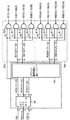
図32は、従来の半導体記憶装置9000における全体構成を示す図である。図32に示す従来の半導体記憶装置9000は、レジスタ901、ロウアドレスバッファ902、ロウプリデコーダ212、冗長判定回路211、メモリセルアレイ910、コラムデコーダ903、およびデータ入出力バッファ904を含む。従来の半導体記憶装置9000は、階層ワード線方式、シェアドセンスアンプ方式の構成を備える。
【0004】
メモリセルアレイ910は、複数のメモリブロック1.0、1.1、…を含む。各メモリブロックは、正規のメモリセルから構成されるノーマルブロック(図中記号NBL(0)、NBL(1)、…)と冗長セルから構成される冗長ブロック(図中記号RBL(0)、RBL(1)、…)とを含む。メモリブロック1.0、…の各々を挟む領域に、センスアンプブロック2が配置される。隣接するメモリブロック同士は、センスアンプブロック2を共有する。
【0005】
レジスタ901は、外部から信号(外部ロウアドレスストローブ信号/RAS、外部コラムアドレスストローブ信号/CAS、外部チップセレクト信号/CS、外部ライトイネーブル信号/WE、外部クロック信号CLK、外部クロックイネーブル信号/CKE等)を受けて、対応する制御信号を出力する。
【0006】
ロウアドレスバッファ902は、外部アドレス信号A0〜Aiに応答して、ロウアドレス信号を出力する。
【0007】
ロウプリデコーダ212は、冗長判定回路211から出力されるイネーブル信号PDEに応答して、ロウアドレスバッファ902の出力に基づき、メインワード線MWLを指定するデコード信号を出力する。また、ロウプリデコーダ212は、ロウアドレスバッファ902の出力に基づき、対応するブロック選択信号を出力する。
【0008】
データ入出力バッファ904は、コラムデコーダ903の制御に基づき、データI/OピンDQ0〜DQnとメモリセルアレイ910との間で信号の授受を行う。
【0009】
メモリセルアレイ910に対して、SDドライバ/SAドライバ924およびMWLドライバ925を配置する。SDドライバ/SAドライバ924は、センスアンプの活性化を制御するシェアードゲート信号、およびワード線を活性化するサブデコード信号を出力する。MWLドライバ925は、メインワード線を選択状態にする。
【0010】
冗長判定回路211は、冗長使用/未使用を判定する。冗長使用の場合には、冗長メインワード線RMWLを選択状態とするための冗長メインワード線選択信号を出力する。
【0011】
メモリブロック1.0、…のそれぞれに対して、図33に示すWLドライバ914を配置する。
【0012】
図33は、図32に示す従来の半導体記憶装置におけるWLドライバ914の構成を示す図であり、参考のため、メモリブロック1.1およびセンスアンプブロックを示している。
【0013】
メモリブロック1.1は、複数の冗長およびノーマルメモリセルMC、複数のビット線対BL(0)および/BL(0)、…、複数のワード線WL(n)、WL(n+1)、…、複数のスペアワード線SWL(0)、SWL(1)、…を含む。複数のビット線対は、各列に対応して配置される。複数のワード線およびスペアワード線は、各行に対応して配置される。
【0014】
メモリブロック1.1に対応してセンスアンプブロック(図中記号2a、2b)を配置する。センスアンプブロック2a、2bはそれぞれ、複数のセンスアンプS/Aと、PMOSトランジスタPT10を構成要素とする複数のイコライズ回路と、NMOSトランジスタNT10、NT11、NT12およびNT13を構成要素とする複数のS/Aシェア回路とを含む。
【0015】
WLドライバ914は、メインワード線MWL(0)、…、MWL(m)または冗長メインワード線RMWL、およびサブデコード信号SD(0)、/SD(0)、SD(1)、/SD(1)、…に基づき、1つのワード線WL(n)、WL(n+1)、またはスペアワード線SWL(0)、SWL(1)を選択状態とする。冗長メインワード線およびスペアワード線は、冗長セルを選択するために使用する。
【0016】
WLドライバ914は、各ワード線およびスペアワード線に対応して、PMOSトランジスタPT1、ならびにNMOSトランジスタNT1およびNMOSトランジスタNT2を備える。たとえば、ワード線WL(0)に対し、PMOSトランジスタPT1の一方の端子は、サブデコード信号SD(1)を受け、他方の端子は、NMOSトランジスタNT1の一方の端子と接続される。PMOSトランジスタPT1およびNMOSトランジスタNT1のそれぞれのゲート電極は、メインワード線MWLと接続される。PMOSトランジスタPT1とNMOSトランジスタNT1との接続ノードは、ワード線WL(0)と接続される。NMOSトランジスタNT2の一方の端子は、ワード線WL(0)と接続され、他方の端子は、接地電位と接続され、そのゲート電極は、サブデコード信号SD(1)を反転したサブデコード信号/SD(1)を受ける。この結果、サブデコード信号または冗長ワブデコード信号により、いずれか一のワード線またはスペアワード線が選択状態になる。
【0017】
【発明が解決しようとする課題】
ところで、冗長領域を配置するメモリセルアレイは、半導体記憶装置にとって必須の構成となっている。この点で、特に、図32に示す従来の半導体記憶装置9000は、メモリブロック間を超えて置換が可能あるという点で救済効率の高い構成を備えているといえる。
【0018】
しかしながら、一般に、冗長セルを含む半導体記憶装置においては、冗長判定があるまで活性化させるブロックが決定されず、高速アクセスが不十分であるという問題がある。
【0019】
この問題点を、図32に示す従来の半導体記憶装置を具体例として、図34を用いて説明する。図34は、図32に示す従来の半導体記憶装置9000における動作を説明するためのタイミングチャートである。
【0020】
図34を参照して、バンク活性信号ACTにより、ロウ系の動作が開始される。アドレス信号RA0〜RA12がラッチされ、ワード線またはスペアワード線の選択、センスアンプの活性化の動作が行なわれる。ワード線の選択時には、冗長の使用・未使用の判定が行なわれる。
【0021】
時刻t0において、ロウアドレスが冗長判定回路211およびロウプリデコーダ212に到達する。τ0の期間、冗長判定が行なわれる。冗長判定後、時刻t1において、対応するワード線またはスペアワード線を選択状態にするためのサブデコード信号または冗長サブデコード信号の活性化、ならびにセンスアンプの準備を行う。
【0022】
具体的には、メモリブロック1.1が選択されると、その両端に位置するセンスアンプブロックが活性状態となる。その動作の準備として、ビット線のイコライズを解除するために、イコライズ信号BLEQをLレベルにし、シェアードゲートをオフするために、シェアードゲートSHR(U)およびSHE(D)をLレベルにする。これらの動作は、冗長判定後、ワード線を立上げるまでに完了する。
【0023】
この結果、最終的にロウアドレスの入力からワード線の立上げまでにτ0+τ20(ただし、τ20=t2−t0)が必要とされる。
【0024】
さらなる問題として、冗長セルを使用した場合、レイアウト面積が増大するという問題が存在する。
【0025】
そこで、本発明はかかる問題を解決するためになされたものであり、その目的は、冗長セルを有する半導体記憶装置において、高速動作が可能な半導体記憶装置を提供することにある。
【0026】
さらに、本発明の他の目的は、レイアウト面積を抑えながら、救済効率の高い半導体記憶装置を提供することにある。
【0027】
【課題を解決するための手段】
請求項1に係る半導体記憶装置は、複数のメモリブロックを備え、複数のメモリブロックの各々は、行列状に配置される複数の正規のメモリセルと、行に対応して配置される複数のワード線と、列に対応して配置される複数のビット線とを含むノーマルブロックを含み、複数のメモリブロックのうち、少なくとも1以上のメモリブロックは、行列状に配置される複数の冗長セルと、行に対応して配置される複数の冗長ワード線と、列に対応して配置される複数のビット線とを含む冗長ブロックをさらに含み、複数の冗長セルは、複数のメモリブロックのいずれかに属する正規のメモリセルを置換するために使用され、外部アドレス信号に応答して、冗長使用か否かを判定する判定手段と、判定手段の判定結果と独立して、外部アドレス信号に応答して、対応するワード線を選択状態にするための制御を行う第1の制御手段と、判定手段の判定結果と独立して、外部アドレス信号に応答して、対応する冗長ワード線を選択状態にするための制御を行う第2制御手段とをさらに備え、第1の制御手段は、判定手段による冗長判定の結果を受けて、対応するワード線を非選択状態にするための制御を行ない、第2の制御手段は、判定手段による冗長未使用の判定の結果を受けて、対応する冗長ワード線を非選択状態にするための制御を行なう。
【0033】
請求項2に係る半導体記憶装置は、請求項1に係る半導体記憶装置であって、第1の制御手段は、外部アドレス信号に対応するワード線を活性化するためのワード線活性化信号を発生する第1の信号発生手段と、複数のノーマルブロックにおける複数のワード線のそれぞれに対応して設けられ、対応するワード線活性化信号に応答して、対応するワード線を選択状態とする複数の正規セル選択手段とを含み、第2の制御手段は、外部アドレス信号に対応する冗長ワード線を活性化するための冗長ワード線活性化信号を発生する第2の信号発生手段と、複数の冗長ブロックにおける複数の冗長ワード線のそれぞれに対応して設けられ、対応する冗長ワード線活性化信号に応答して、対応する冗長ワード線を選択状態とする複数の冗長セル選択手段とを含み、第1の信号発生手段は、判定手段から受ける冗長判定の結果に応答して、活性化したワード線活性化信号を非活性化し、第2の信号発生手段は、判定手段から受ける冗長未判定の結果に応答して、活性化した冗長ワード線の活性化信号を非活性化する。
【0034】
請求項3に係る半導体記憶装置は、請求項1に係る半導体記憶装置であって、複数のメモリブロックおよび複数の冗長ブロックのそれぞれに対応して設けられる複数のセンスアンプブロックをさらに備え、複数のセンスアンプブロックのそれぞれは、複数のセンスアンプ手段を含み、複数のセンスアンプ手段のそれぞれは、対応するビット線の電位を増幅する手段と、対応するビット線の電位を均一化するイコライズ回路と、非選択のメモリブロック側に対応するビット線を分離するS/Aシェア回路とを含み、第1の制御手段は、外部アドレス信号に応答して、対応するノーマルブロックにおけるセンスアンプブロックの活性化を制御する第1の制御信号を発生し、第2の制御手段は、外部アドレス信号に応答して、対応する冗長ブロックにおけるセンスアンプブロックの活性化を制御する第2の制御信号を発生し、第1の信号発生手段は、判定手段から受ける冗長判定の結果に応答して、発生した第1の制御信号のレベルを変化させ、第2の信号発生手段は、判定手段から受ける冗長未判定の結果に応答して、発生した第2の制御信号のレベルを変化させる。
【0035】
請求項4に係る半導体記憶装置は、請求項3に係る半導体記憶装置であって、第1の制御手段は、外部アドレス信号に対応するワード線を活性化するためのワード線活性化信号を発生する第1の信号発生手段と、複数のノーマルブロックにおける複数のワード線のそれぞれに対応して設けられ、対応するワード線活性化信号に応答して、対応するワード線を選択状態とする複数の正規セル選択手段とをさらに含み、第2の制御手段は、外部アドレス信号に対応する冗長ワード線を活性化するための冗長ワード線の活性化信号を発生する第2の信号発生手段と、複数の冗長ブロックにおける複数の冗長ワード線のそれぞれに対応して設けられ、対応する冗長ワード線活性化信号に応答して、対応する冗長ワード線を選択状態とする複数の冗長セル選択手段とをさらに含み、第1の信号発生手段は、判定手段から受ける冗長判定の結果に応答して、活性化したワード線活性化信号を非活性化し、第2の信号発生手段は、判定手段から受ける冗長未判定の結果に応答して、活性化した冗長ワード線活性化信号を非活性化する。
【0036】
請求項5に係る半導体記憶装置は、請求項1に係る半導体記憶装置であって、第1の制御手段は、外部アドレス信号に対応するワード線を活性化するための第1レベルのワード線活性化信号を発生する第1の信号発生手段と、冗長手段から受ける冗長未使用の判定結果に応答して、第1レベルのワード線活性化信号のレベルを活性レベルに立上げる手段と、複数のノーマルブロックにおける複数のワード線のそれぞれに対応して設けられ、対応するワード線活性化信号に応答して、対応するワード線を選択状態とする複数の正規セル選択手段とを含み、第2の制御手段は、外部アドレス信号に対応する冗長ワード線を活性化するための第1レベルの冗長ワード線活性化信号を発生する第2の信号発生手段と、冗長手段から受ける冗長使用の判定結果に応答して、第1レベルの冗長ワード線活性化信号のレベルを活性レベルに立上げる手段と、複数の冗長ブロックにおける複数の冗長ワード線のそれぞれに対応して設けられ、対応する冗長ワード線活性化信号に応答して、対応する冗長ワード線を選択状態とする複数の冗長セル選択手段とを含み、第1の信号発生手段は、判定手段から受ける冗長判定の結果に応答して、活性化したワード線活性化信号を非活性化し、第2の信号発生手段は、判定手段から受ける冗長未判定の結果に応答して、活性化した冗長ワード線活性化信号を非活性化する。
【0037】
請求項6に係る半導体記憶装置は、請求項5に係る半導体記憶装置であって、第1レベルとは、活性レベルと非活性レベルとの実質的に中間の値である。
【0038】
請求項7に係る半導体記憶装置は、請求項2に係る半導体記憶装置であって、複数のワード線の各々は、メインワード線と、メインワード線の各々に対応して設けられる複数のサブワード線とを含み、複数の冗長ワード線の各々は、冗長メインワード線と、冗長メインワード線の各々に対応して設けられる複数のスペアワード線とを含み、ワード線活性化信号は、サブワード線を選択状態とし、冗長ワード線活性化信号は、スペアワード線を選択状態とする。
【0039】
請求項8に係る半導体記憶装置は、請求項4に係る半導体記憶装置であって、複数のワード線の各々は、メインワード線と、メインワード線の各々に対応して設けられる複数のサブワード線とを含み、複数の冗長ワード線の各々は、冗長メインワード線と、冗長メインワード線の各々に対応して設けられる複数のスペアワード線とを含み、ワード線活性化信号は、サブワード線を選択状態とし、冗長ワード線活性化信号は、スペアワード線を選択状態とする。
【0040】
請求項9に係る半導体記憶装置は、行列状に配置される複数の正規のメモリセルと、行に対応して配置される複数のワード線と、列に対応して配置される複数のビット線とを含むノーマルブロックと、行列状に配置され、対応する正規のメモリセルと置換するための複数の冗長セルと、行に対応して配置される複数の冗長ワード線と、列に対応して配置される複数のビット線とを含む冗長ブロックと、外部アドレス信号に応答して、冗長使用か否かを判定する判定手段と、判定手段の判定結果と独立して、外部アドレス信号に応答して、対応するワード線を選択状態にするための制御を行う第1の制御手段と、判定手段の判定結果と独立して、外部アドレス信号に応答して、対応する冗長ワード線を選択状態にするための制御を行う第2制御手段とをさらに備え、第1の制御手段は、判定手段による冗長判定の結果を受けて、対応するワード線を非選択状態にするための制御を行ない、第2の制御手段は、判定手段による冗長未使用の判定の結果を受けて、対応する冗長ワード線を非選択状態にするための制御を行なう。
【0041】
請求項10に係る半導体記憶装置は、請求項9に係る半導体記憶装置であって、第1の制御手段は、外部アドレス信号に対応するワード線を活性化するための第1レベルのワード線活性化信号を発生する第1の信号発生手段と、冗長手段から受ける冗長未使用の判定結果に応答して、第1レベルのワード線活性化信号のレベルを活性レベルに立上げる手段と、複数のワード線のそれぞれに対応して設けられ、対応するワード線活性化信号に応答して、対応するワード線を選択状態とする複数の正規セル選択手段とを含み、第2の制御手段は、外部アドレス信号に対応する冗長ワード線を活性化するための第1レベルの冗長ワード線活性化信号を発生する第2の信号発生手段と、冗長手段から受ける冗長使用の判定結果に応答して、第1レベルの冗長ワード線活性化信号のレベルを活性レベルに立上げる手段と、複数の冗長ワード線のそれぞれに対応して設けられ、対応する冗長ワード線活性化信号に応答して、対応する冗長ワード線を選択状態とする複数の冗長セル選択手段とを含み、第1の信号発生手段は、判定手段から受ける冗長判定の結果に応答して、活性化したワード線活性化信号を非活性化し、第2の信号発生手段は、判定手段から受ける冗長未判定の結果に応答して、活性化した冗長ワード線活性化信号を非活性化する。
【0042】
請求項11に係る半導体記憶装置は、請求項10に係る半導体記憶装置であって、第1レベルとは、活性レベルと非活性レベルとの実質的に中間の値である。
【0043】
請求項12に係る半導体記憶装置は、請求項11に係る半導体記憶装置であって、外部アドレス信号をデコードするデコード手段をさらに備え、第1の制御手段は、デコード手段の出力するデコード信号に応答して、第1レベルのワード線活性化信号を発生し、第2の制御手段は、デコード手段の出力するデコード信号に応答して、第1レベルの冗長ワード線活性化信号を発生する。
【0047】
【発明の実施の形態】
[実施の形態1]
本発明の実施の形態1における半導体記憶装置について説明する。本発明の実施の形態1における半導体記憶装置は、メモリブロック間を超えて置換可能な半導体記憶装置に関し、通常のロウアドレス系と冗長用のロウアドレス系とを個別に制御することにより、アクセス時間の高速化を図るものである。
【0048】
本発明の実施の形態1における半導体記憶装置の全体構成について図1を用いて説明する。図1は、本発明の実施の形態1における半導体記憶装置1000の全体構成を示す図である。従来の半導体記憶装置9000と同じ構成要素には、同じ符号、同じ記号を付し、その説明を省略する。
【0049】
図1に示す半導体記憶装置1000は、レジスタ901、ロウアドレスバッファ902、ロウアドレス系デコード回路21、コラムデコーダ903、メモリセルアレイ910、およびデータ入出力バッファ904を含む。図1に示す半導体記憶装置1000は、階層ワード線方式、シェアドセンスアンプ方式の構成を備える。
【0050】
メモリセルアレイ910は、複数のメモリブロック1.0、1.1、…を含む。各メモリブロックは、正規のメモリセルから構成されるノーマルブロック(図中記号NBL(0)、NBL(1)、…)と冗長セルから構成される冗長ブロック(図中記号RBL(0)、RBL(1)、…)とを含む。半導体記憶装置1000では、1のメモリブロックに対して、他のメモリブロックに存在する冗長ブロックを使用して置換を行なうことが可能である。
【0051】
メモリブロック1.0、…のそれぞれを挟む領域に、センスアンプブロック2が配置される。隣接するメモリブロック同士は、センスアンプブロック2を共有する。メモリブロック1.0、…のそれぞれに対して、WLドライバ4を配置する。
【0052】
なお、以下の説明においては、16組のメモリブロック、64本のメインワード線、および8組のサブデコード信号から1本のワード線が選択されるものとする。また、各メモリブロック毎に、1本の冗長メインワード線と8組の冗長サブデコード信号とから1本のスペアワード線が選択されるものとする。
【0053】
ロウアドレス系デコード回路21は、冗長判定回路20、ロウプリデコーダ22、ブロック選択回路23、SDドライバ/SAドライバ24、およびMWLドライバ25を含む。冗長判定回路20は、レジスタ901から受けるアクト信号ACTに応答して、アドレスバッファ902から受けるアドレス信号に基づき、冗長判定を行う。判定結果として、判定信号RHIT、信号RMWL、および冗長ブロックを指定するプリデコード信号RSDF(図中記号RSDF(0)〜RSDF(15))を出力する。
【0054】
冗長判定回路20から出力される判定信号RHITは、初期状態でLレベルである。冗長を使用した場合は、判定信号RHITは、Hレベルとなり、いずれか1のプリデコード信号RSDFがHレベルとなる。冗長未使用の場合は、判定信号RHITおよびプリデコード信号RSDFはLレベルを保持する。ロウプリデコーダ22は、ロウアドレスバッファ902の出力をデコードする。
【0055】
ブロック選択回路23は、冗長判定回路20から出力される判定信号RHITに応答して、アドレスバッファ902の出力に基づき、ノーマルブロックに対応するブロック選択信号を出力する。
【0056】
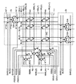
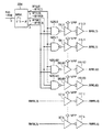
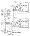
図2は、図1に示す本発明の実施の形態1におけるWLドライバ4の構成を示す図であり、参考のため、メモリブロック1.1およびセンスアンプブロックを示している。
【0057】
メモリブロック1.1に対応してセンスアンプブロック(図中記号2a、2b)を配置する。センスアンプブロック2aおよび2bはそれぞれ、複数のセンスアンプS/Aと、PMOSトランジスタPT10を構成要素とする複数のイコライズ回路と、NMOSトランジスタNT10、NT11、NT12およびNT13を構成要素とする複数のS/Aシェア回路とを含む。PMOSトランジスタPT10は、イコライズ信号BLEQに応答してオン/オフする。NMOSトランジスタNT10およびNT11は、シェアードゲート信号SHR(U)に応答してオン/オフする。NMOSトランジスタNT12およびNT13は、シェアードゲート信号SHR(D)に応答してオン/オフする。
【0058】
WLドライバ4は、ノーマルブロックに対するドライバ4bに加えて、冗長ブロックに対するドライバ4bを備える。ドライバ4bの構成は、図33で説明した構成と同じである。
【0059】
ドライバ4bは、メインワード線MWL(0)、…、MWL(m)、ならびにサブデコード信号SD(0)および/SD(0)、SD(1)および/SD(1)、…に基づき、1つのワード線WL(n)、WL(n+1)、…を選択状態とする。
【0060】
ドライバ4aは、冗長メインワード線RMWL、ならびに冗長サブデコード信号RSD(0)および/RSD(0)、RSD(1)および/RSD(1)、…に基づき、1つのスペアワード線SWL(0)、SWL(1)、…を選択状態とする。
【0061】
ドライバ4aは、各スペアワード線に対応して、PMOSトランジスタPT2、ならびにNMOSトランジスタNT4およびNT5を備える。たとえば、スペアワード線SWL(0)に対し、PMOSトランジスタPT2の一方の端子は、冗長サブデコード信号RSD(1)を受け、他方の端子は、NMOSトランジスタNT4の一方の端子と接続される。PMOSトランジスタPT2およびNMOSトランジスタNT4のそれぞれのゲート電極は、冗長メインワード線RMWLと接続される。NMOSトランジスタNT4の他方の端子は、接地電位と接続される。
【0062】
PMOSトランジスタPT2とNMOSトランジスタNT4との接続ノードは、スペアワード線SWL(0)と接続される。NMOSトランジスタNT5の一方の端子は、スペアワード線SWL(0)と接続され、他方の端子は、接地電位と接続され、そのゲート電極は、冗長サブデコード信号/RSD(1)を受ける。スペアワード線とワード線とは、異なる経路で選択される。
【0063】
図3は、図1に示す本発明の実施の形態1におけるロウアドレス系デコード回路21の主要部の構成を示す図である。
【0064】
図3に示すプリデコーダ22aおよび22b、ならびにMWLプリデコーダ22cは、図1に示すロウプリデコーダ22に含まれる。プリデコーダ22aは、4ビットのアドレス信号RA9〜RA12に応答して、16ビットのプリデコード信号XF2(図中記号XF2(0)〜XF2(15))を出力する。
【0065】
プリデコーダ22bは、3ビットのアドレス信号RA0〜RA2に応答して、8ビットのプリデコード信号XF0(図中記号XF0(0)〜XF0(7))を出力する。
【0066】
MWLプリデコーダ22cは、判定信号RHITに応答して、6ビットのアドレス信号RA3〜RA8に基づき、メインワード線を指定するプリデコード信号を出力する。
【0067】
図4は、図3に示す本発明の実施の形態1におけるMWLプリデコーダ22cの構成を示す図である。MWLプリデコーダ22cは、3組のデコード回路28a、28b、および28cを含む。
【0068】
デコード回路28aは、アドレス信号RA3、/RA3、RA4および/RA4に応答して、プリデコード信号XF1L(0)〜(3)を出力する。デコード回路28bは、アドレス信号RA5、/RA5、RA6および/RA6に応答して、プリデコード信号XF1M(0)〜(3)を出力する。デコード回路28cは、アドレス信号RA7、/RA7、RA8および/RA8に応答して、プリデコード信号XF1H(0)〜(3)を出力する。
【0069】
デコード回路28a、28b、および28cのそれぞれは、NAND回路N4、N5、N6およびN7、ならびにインバータI3、I4、I5およびI6を含む。
【0070】
デコード回路28aを代表例としてその構成を説明する。NAND回路N4は、アドレス信号RA3とアドレス信号/RA4とを入力に受ける。インバータI3は、NAND回路N4の出力を反転して、プリデコード信号XF1L(0)を出力する。NAND回路N5は、アドレス信号/RA4とアドレス信号/RA3とを入力に受ける。インバータI4は、NAND回路N5の出力を反転して、プリデコード信号XF1L(1)を出力する。NAND回路N6は、アドレス信号RA3とアドレス信号RA4とを入力に受ける。インバータI5は、NAND回路N6の出力を反転して、プリデコード信号XF1L(2)を出力する。NAND回路N7は、アドレス信号/RA3とアドレス信号RA4とを入力に受ける。インバータI6は、NAND回路N7の出力を反転して、プリデコード信号XF1L(3)を出力する。
【0071】
図3におけるSDドライバ26.0、…は、図1に示すSDドライバ/SAドライバ24に含まれる。SDドライバ26.0、…は、メモリブロックのそれぞれに対応して配置する。
【0072】
SDドライバ26.0、…のそれぞれは、NAND回路N1およびN2、レベル変換回路S1、ならびにインバータI1を含む。NAND回路N1は、プリデコーダ22aおよび22bの出力を受ける。インバータI0は、判定信号RHITを反転して、信号/RHITを出力する。NAND回路N2の一方のノードは、信号/RHITを受け、他方のノードは、NAND回路N1の出力を受ける。
【0073】
NAND回路N2は、対応するノーマルブロックにおけるサブデコード信号/SD(図中記号/SD0(i)、…:i=0〜7)を出力する。インバータI1は、レベル変換回路S1を介して、NAND回路N2の出力を受け、対応するノーマルブロックにおけるサブデコード信号SD(図中記号SD0(i)、…:i=0〜7)を出力する。
【0074】
SDドライバ26.0、…のそれぞれはさらに、NAND回路N3、レベル変換回路S2、およびインバータI2を含む。NAND回路N3は、プリデコーダ22bの出力と冗長判定回路20から出力される16ビットのプリデコード信号RSDF(0)〜RSDF(15)とを受ける。
【0075】
NAND回路N3は、対応する冗長ブロックにおける冗長サブデコード信号/RSD(図中記号/RSD0(i)、…:i=0〜7)を出力する。インバータI2は、レベル変換回路S2を介して、NAND回路N3の出力を受け、対応する冗長ブロックにおける冗長サブデコード信号RSD(図中記号RSD0(i)、…i=0〜7)を出力する。
【0076】
図3に示すMWLドライバ25.n(n=0〜15)は、1のメモリブロックに対応するものであり、他のメモリブロックに対応するMWLドライバとともに、図1に示すMWLドライバ25に含まれる。
【0077】
MWLドライバ25.nは、MWLプリデコーダ22cの出力と、冗長判定回路20から出力される信号RMWLおよびプリデコード信号RSDF(0)〜RSDF(15)とに応答して、対応するメモリブロックのメインワード線選択信号または、冗長メインワード線選択信号を出力する。これにより、メインワード線MWL(0)〜MWL(m) または冗長メインワード線RMWLが選択状態になる。
【0078】
図5は、本発明の実施の形態1におけるMWLドライバの構成を示す図であり、代表例として、1のメモリブロックに対応するMWLドライバ25.nの構成を示す。なお、参考のため、プリデコーダ22cおよび冗長判定回路20を併せて示している。
【0079】
MWLドライバ25.nは、NAND回路N8.0、…、N8.63、レベル変換回路S3.0、…、S3.63、およびインバータI7.0、…、I7.63を含む。NAND回路N8.0、…、N8.63、レベル変換回路S3.0、…、S3.63、およびインバータI7.0、…、I7.63のそれぞれは、メインワード線に対応して配置する。
【0080】
たとえば、NAND回路N8.0は、MWLプリデコーダ22cから対応するプリデコード信号XF1L(0)〜(3)、XF1H(0)〜(3)、XF1M(0)〜(3)を受ける。インバータI7.0は、対応するレベル変換回路S3.0を介してNAND回路N8.0の出力を受け、メインワード線選択信号/MWL(0)を出力する。対応するメインワード線MWL(0)は、メインワード線選択信号/MWL(0)を受けて選択状態となる。
【0081】
MWLドライバ25.nはさらに、レベル変換回路S4およびインバータI8を含む。レベル変換回路S4およびインバータI8は、冗長ブロックにおける冗長メインワード線に対応して配置する。
【0082】
レベル変換回路S4は、冗長判定回路20から信号RMWLを受ける。インバータI8は、対応するレベル変換回路S4の出力を反転して、冗長メインワード線選択信号/RMWLを出力する。対応する冗長メインワード線RMWLは、冗長メインワード線選択信号/RMWLを受けて選択状態となる。
【0083】
次に、本発明の実施の形態1における半導体記憶装置1000の動作について、タイミングチャートである図6を参照して説明する。
【0084】
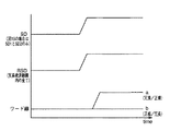
図6は、本発明の実施の形態1における半導体記憶装置1000の動作を説明するためのタイミングチャートである。
【0085】
外部制御信号に応答して、アクト信号ACTがHレベルの活性状態になり、ロウアドレス信号が取込まれる。この時点で、判定信号RHITは、Lレベルの状態にある。
【0086】
時刻t0において、アドレス信号をプリデコードしたプリデコード信号XF2、XF0のなかのいずれか1つがHレベルの状態になる。
【0087】
これにより、対応するサブデコード信号SDおよび/SDが活性化される。さらに対応するメインワード線を選択するメインワード線選択信号が活性化される。この間、冗長判定回路20は、冗長判定処理の状態にある。
【0088】
時刻t1において、判定結果として判定信号RHITが出力される。冗長未使用の場合、判定信号RHITは、Lレベルを保持する(実線部分)。この場合、冗長判定回路20の出力であるプリデコード信号RSDFはLレベルのままである。
【0089】
冗長使用の場合、判定信号RHITがHレベルに立上がる(点線部分)。これにより、活性化されたサブデコード信号SDおよび/SDが、非活性化される(点線部分)。置換されたスペアワード線の存在する冗長ブロックを指定するプリデコード信号RSFDがHレベルに立上がる。
【0090】
一方、対応する冗長サブデコード信号RSDおよび/RSDが活性化される。さらに、これをトリガとして、対応する冗長メインワード線を選択する冗長メインワード線選択信号が活性状態となる。
【0091】
このように構成することにより、冗長未使用時の場合、ノーマルブロックに対するサブデコード信号SDの活性化は、時刻t0〜t1の冗長判定期間τ0に完了し、ワード線の立上げは、メインワード線選択信号の到達にのみ律足されることになる。
【0092】
一方、冗長使用時については、冗長用のワード線ドライバ(ドライバ4a)の数は、正規のワード線ドライバ(ドライバ4b)の数より少なく(1対64)、冗長用のドライバに係る負荷容量は、正規のドライバにかかる負荷容量より小さい。
【0093】
また、冗長サブデコード線の活性化速度は速く、冗長サブデコード線の立上がり速度は、メインワード線の立上がり速度と同等もしくはそれ以上である。メインワード線はサブデコード線と比較して容量が小さいため、ワード線の立上がり速度が速くなる(τ2は、図34におけるτ20より短くなる)。
【0094】
この結果、特にメモリブロック間を超えて置換可能な冗長ブロックを含む半導体記憶装置において、アクセス時間の短縮化を図ることが可能となる。
【0095】
[実施の形態2]
本発明の実施の形態2における半導体記憶装置について説明する。本発明の実施の形態1における半導体記憶装置1000は、ノーマルブロックのロウアクセスと冗長ブロックのロウアクセスとを分離して制御することにより、高速アクセスを実現するものである。しかしながら、本発明の実施の形態1における構成では、SDドライバからWLドライバへの配線、WLドライバ上の配線、およびSDドライバの数のが、それぞれ従来に比べて増加するため、レイアウト面積が増大してしまう。
【0096】
そこで、本発明の実施の形態2においては、隣接するメモリブロック間で、サブデコード信号(正規および冗長いずれも)を共有する。これにより、アクセスの高速化およびレイアウト面積の縮小化を可能とする。
【0097】
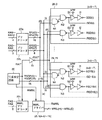
本発明の実施の形態2における半導体記憶装置の主要部の構成について、図7を用いて説明する。図7は、本発明の実施の形態2における半導体記憶装置1200の主要部の構成の一例を示す図である。
【0098】
図7に示す半導体記憶装置1200は、複数のメモリブロック1.0、…、1.15を含む。各メモリブロックに対応して、MWLデコーダ/ドライバ31を配置する。
【0099】
メモリブロック1.0、…のそれぞれを挟む領域に、図示しないセンスアンプブロックを配置する。隣接するメモリブロック同士は、センスアンプブロックを共有する。
【0100】
各メモリブロックは、ノーマルブロック(図中記号NBL(0)、NBL(1)、…)と冗長ブロック(図中記号RBL(0)、RBL(1)、…)とを含む。1のメモリブロックに対して、他のメモリブロックに存在する冗長ブロックを使用して置換を行なうことが可能である。
【0101】
冗長ブロックをメモリブロックの端部に配置し、隣接するメモリブロック間において、互いの冗長ブロックがセンスアンプブロックを挟んで向い合うように配置する。
【0102】
冗長サブデコード信号RSDを活性化するSDローカルドライバ32aは、冗長ブロックに挟まれたセンスアンプブロックに配置する。ノーマルブロックに対するサブデコード信号SDを活性化するSDローカルドライバ32bは、ノーマルブロックに挟まれたセンスアンプブロックに配置する。
【0103】
SDローカルドライバ32aおよび32bのそれぞれは、各々を挟むように位置するノーマルブロックまたは冗長ブロックに対応して配置される。具体的には、冗長ブロックRBL(0)およびRBL(1)の間に位置するSDローカルドライバ32aは、両メモリブロックにおける冗長サブデコード信号RSDを活性化するために用いる。ノーマルブロックNBL(1)およびNBL(2)の間に位置するSDローカルドライバ32bは、両メモリブロックにおけるサブデコード信号SDを活性化するために用いる。
【0104】
SDローカルドライバ32bおよび32aの並びに対して、SDドライバ33を配置する。
【0105】
図8は、図7に示す本発明の実施の形態2におけるSDローカルドライバの構成の一例を示す図であり、一例として、メモリブロック1.1および1.2におけるノーマルブロックに対応するSDローカルドライバ32bと、メモリブロック1.0および1.1における冗長ブロックに対応するSDローカルドライバ32aの構成を示す。
【0106】
SDローカルドライバに対しては、ロウプリデコーダ35およびブロック選択回路/SDドライバ34を配置する。
【0107】
ロウプリデコーダ35は、1ビットのアドレス信号RA9に応答して、2ビットのプリデコード信号XF2L(図中記号XF2L(0)〜XF2L(1))を出力する。プリデコード信号XF2Lは、2つのメモリブロックのうちの1つを選択する。
【0108】
さらに、ロウプリデコーダ35は、3ビットのアドレス信号RA10〜RA12に応答して、ノーマルブロックに対する8ビットのプリデコード信号XF2H(図中記号XF2H(0)〜XF2H(7))を出力する。また、ロウプリデコーダ35は、3ビットのアドレス信号RA0〜RA2に応答して、冗長ブロックに対する8ビットのプリデコード信号XF0(図中記号XF0(0)〜XF0(7))を出力する。
【0109】
ブロック選択回路/SDドライバ34は、プリデコード信号XF2Hに応答して、共通サブデコード信号SD1/2(図中記号、SD1/2(0)〜SD1/2(7))およびこれらを反転した信号/SD1/2(図中記号/SD1/2(0)〜/SD1/2(7))を出力する。
【0110】
ブロック選択回路/SDドライバ34は、プリデコード信号XF0に応答して、共通冗長サブデコード信号RSD0/1(図中記号、RSD0/1(0)〜RSD0/1(7))およびこれらを反転した信号/RSD0/1(図中記号/RSD0/1(0)〜/RSD0/1(7))を出力する。
【0111】
SDローカルドライバ32bは、NAND回路N10、N11、N12、およびN13を含む。NAND回路N10は、ノーマルブロックNBL(1)のサブデコード信号SD1(0)〜SD1(7)に対応して配置する。NAND回路N11は、ノーマルブロックNBL(2)のサブデコード信号SD2(0)〜SD2(7)に対応して配置する。
【0112】
NAND回路N12は、ノーマルブロックNBL(1)のサブデコード信号/SD1(0)〜/SD1(7)に対応して配置する。NAND回路N13は、ノーマルブロックNBL(2)のサブデコード信号/SD2(0)〜/SD2(7)に対応して配置する。
【0113】
NAND回路N10およびN12のそれぞれの一方の入力ノードは、プリデコード信号XF2L(0)を受ける。NAND回路N11およびN13のそれぞれの一方の入力ノードは、プリデコード信号XF2L(1)を受ける。NAND回路N10およびN11のそれぞれの他方の入力ノードは、共通サブデコード信号SD1/2を受ける。NAND回路N12およびN13のそれぞれの他方の入力ノードは、共通サブデコード信号/SD1/2を受ける。
【0114】
NAND回路N10およびN12のそれぞれから、ノーマルブロックNBL(1)に対するサブデコード信号SD1(0)〜SD1(7)、/SD1(0)〜/SD1(7)がそれぞれ出力される。NAND回路N11およびN13のそれぞれから、ノーマルブロックNBL(2)に対するサブデコード信号SD2(0)〜SD2(7)、/SD2(0)〜/SD2(7)が出力される。
【0115】
SDローカルドライバ32aは、NAND回路N14、N15、N16、およびN17を含む。NAND回路N14は、冗長ブロックRBL(0)の冗長サブデコード信号RSD0(0)〜RSD0(7)に対応して配置する。NAND回路N15は、冗長ブロックRBL(1)の冗長サブデコード信号RSD1(0)〜RSD1(7)に対応して配置する。NAND回路N16は、冗長ブロックRBL(0)の冗長サブデコード信号/RSD0(0)〜/RSD0(7)に対応して配置する。NAND回路N17は、冗長ブロックRBL(1)の冗長サブデコード信号/RSD1(0)〜/RSD1(7)に対応して配置する。
【0116】
NAND回路N14およびN16のそれぞれの一方の入力ノードは、プリデコード信号XF2L(0)を受ける。NAND回路N15およびN17のそれぞれの一方の入力ノードは、プリデコード信号XF2L(1)を受ける。NAND回路N14およびN15のそれぞれの他方の入力ノードは、共通冗長サブデコード信号RSD0/1を受ける。NAND回路N16およびN17のそれぞれの他方の入力ノードは、共通冗長サブデコード信号/RSD0/1を受ける。
【0117】
NAND回路N14およびN16のそれぞれから、冗長ブロックRBL(0)に対応する冗長サブデコード信号RSD0(0)〜RSD0(7)、/RSD0(0)〜/RSD0(7)がそれぞれ出力される。NAND回路N15およびN17のそれぞれから、冗長ブロックRBL(1)に対応する冗長サブデコード信号RSD1(0)〜RSD1(7)、/RSD1(0)〜/RSD1(7)がそれぞれ出力される。
【0118】
このように、ノーマルブロックにおけるロウアクセスと冗長ブロックにおけるロウアクセスとを切離して制御することにより、高速アクセスを可能とする。
【0119】
さらに、隣接するメモリブロック間でサブデコード信号SDおよひ冗長サブデコード信号RSDを共有することにより、レイアウト面積を縮小することが可能となる。
【0120】
[実施の形態3]
本発明の実施の形態3における半導体記憶装置について図9を用いて説明する。本発明の実施の形態3における半導体記憶装置は、図7に示す半導体記憶装置1200に対応するものであり、図7および図8に示すSDローカルドライバ32aおよび32bに代えて、図9に示すSDローカルドライバ36aおよび36bを備える。
【0121】
図9は、本発明の実施の形態3におけるSDローカルドライバの構成の一例を示す図であり、一例として、メモリブロック1.1および1.2のノーマルブロックに対応するSDローカルドライバ36bと、メモリブロック1.0および1.1の冗長ブロックに対応するSDローカルドライバ36aの構成を示す。
【0122】
SDローカルドライバに対しては、ロウプリデコーダ35およびブロック選択回路/SDドライバ34を配置する。
【0123】
上述したように、ロウプリデコーダ35は、2ビットのプリデコード信号XF2L(図中記号XF2L(0)〜XF2L(1))、8ビットのプリデコード信号XF2H(図中記号XF2H(0)〜XF2H(7))、および8ビットのプリデコード信号XF0(図中記号XF0(0)〜XF0(7))を出力する。
【0124】
ブロック選択回路/SDドライバ34は、共通サブデコード信号SD1/2(図中記号、SD1/2(0)〜SD1/2(7))およびこれらを反転した信号/SD1/2(図中記号/SD1/2(0)〜/SD1/2(7))、ならびに共通冗長サブデコード信号RSD0/1(図中記号、RSD0/1(0)〜RSD0/1(7))およびこれらを反転した信号/RSD0/1(図中記号/RSD0/1(0)〜/RSD0/1(7))を出力する。
【0125】
SDローカルドライバ36bは、図8に示すNAND回路N10、N11、N12、およびN13のそれぞれに代えて、トランスファーゲートT10、T11、T12、およびT13を備える。
【0126】
トランスファーゲートT10およびT12のそれぞれは、Hレベルのプリデコード信号XF2L(0)に応答して導通状態となる。トランスファーゲートT11およびT13のそれぞれは、Hレベルのプリデコード信号XF2L(1)に応答して導通状態となる。
【0127】
トランスファーゲートT10およびT11のそれぞれの一方の導通端子は、共通サブデコード信号SD1/2を受ける。トランスファーゲートT12およびT13のそれぞれの一方の導通端子は、共通サブデコード信号/SD1/2を受ける。
【0128】
トランスファーゲートT10およびT12のそれぞれの他方の導通端子から、メモリブロック1.1のノーマルブロックNBL(1)に対するサブデコード信号SD1(0)〜SD1(7)、サブデコード信号/SD1(0)〜/SD1(7)がそれぞれ出力される。トランスファーゲートT11およびT13のそれぞれの他方の導通端子から、メモリブロック1.2のノーマルブロックNBL(2)に対するサブデコード信号SD2(0)〜SD2(7)、/SD2(0)〜/SD2(7)がそれぞれ出力される。
【0129】
SDローカルドライバ36bは、図8に示すNAND回路N14、N15、N16、およびN17のそれぞれに代えて、トランスファーゲートT14、T15、T16、およびT17を備える。
【0130】
トランスファーゲートT14およびT16のそれぞれは、Hレベルのプリデコード信号XF2L(0)に応答して導通状態となる。トランスファーゲートT15およびT17のそれぞれは、Hレベルのプリデコード信号XF2L(1)に応答して導通状態となる。
【0131】
トランスファーゲートT14およびT15のそれぞれの一方の導通端子は、共通冗長サブデコード信号RSD0/1を受ける。トランスファーゲートT16およびT17のそれぞれの一方の導通端子は、共通冗長サブデコード信号/RSD0/1を受ける。
【0132】
トランスファーゲートT14およびT15のそれぞれの他方の導通端子から、冗長ブロックRBL(0)に対する冗長サブデコード信号RSD0(0)〜RSD0(7)、/RSD0(0)〜/RSD0(7)がそれぞれ出力される。トランスファーゲートT15およびT17のそれぞれの他方の導通端子から、冗長ブロックRBL(1)に対する冗長サブデコード信号RSD1(0)〜RSD1(7)、/RSD1(0)〜/RSD1(7)がそれぞれ出力される。
【0133】
このように、ノーマルブロックにおけるロウアクセスと冗長ブロックにおけるのロウアクセスとを切離して制御することにより、高速アクセスを可能とする。
【0134】
また、隣接するメモリブロック間でデコーダを共有することにより、レイアウト面積を縮小することが可能となる。
【0135】
さらに、SDローカルデコーダを、構成素子数の多いNAND回路に代えて構成素子の少ないトランスファーゲートで構成することにより、本発明の実施の形態2に比べて、レイアウト面積を縮小することが可能となる。
【0136】
[実施の形態4]
本発明の実施の形態4における半導体記憶装置について説明する。本発明の実施の形態4における半導体記憶装置は、ノーマルブロックに対するサブデコード信号の活性化に加えて、センスアンプ系についても冗長系と切離して制御することにより、さらにアクセス時間の短縮化を図るものである。
【0137】
本発明の実施の形態4における半導体記憶装置について図10を用いて説明する。図10は、本発明の実施の形態4における半導体記憶装置1400の全体構成の一例を示す図である。半導体記憶装置1000および1200と同じ構成要素には、同じ符号および同じ符号を付し、その説明を省略する。
【0138】
図10に示す半導体記憶装置1400は、ロウアドレスバッファ902、プリデコーダ22aおよび22b、MWLプリデコーダ22d、ブロック選択回路45、冗長判定回路46、ならびに複数のメモリブロック1.0、…、1.15を含む。
【0139】
メモリブロック1.0、…のそれぞれを挟む領域に、センスアンプS/Aを配置する。隣接するメモリブロック同士は、センスアンプS/Aを共有する。複数のセンスアンプS/Aを含むセンスアンプブロックに対応して、SDドライバ・S/A帯制御信号用ドライバ42を配置する。SDドライバ・S/A帯制御信号ドライバ42におけるS/A帯制御信号ドライバ部分は、非選択のメモリブロックを分離するためのシェアードゲート信号、およびビット線対をイコライズするためのイコライズ信号を出力する。SDドライバ・S/A帯制御信号ドライバ42におけるSDドライバ部分は、サブデコード信号を活性化する。
【0140】
メモリブロック1.0、…のそれぞれに対して、MWLデコーダ/ドライバ41を配置する。図10における記号WLDは、WLドライバを示す。
【0141】
メモリブロック1.0、…の配列の両端部分に位置するメモリブロック1.0および1、15は、冗長ブロック40aおよび40bを含む。その他のメモリブロック1.1、…、1.14は、冗長ブロックを含まない。メモリブロック1.1、…、1.14のそれぞれは、ノーマルブロックNBL(1)、NBL(2)、…のそれぞれを含む。
【0142】
冗長ブロック40aおよび40bのそれぞれに対応して、冗長用のRMWLドライバ43aおよび43bを配置する。
【0143】
本発明の実施の形態4においては、従来各ブロック毎に分散して配置していた冗長ブロックを、2個所に集中して配置する。スペアワード線SWLは、冗長メインワード線が活性化した場合にのみ活性化される。
【0144】
冗長判定回路46は、アドレス信号RA0〜RA12に基づき、2種類の判定信号RHITおよびRMISを出力する。判定信号RHITおよびRMISは、初期状態においてLレベルである。冗長未使用であると判定された場合、判定信号RMISがHレベルになり、冗長使用であると判定された場合、判定信号RHITがHレベルになる。MWLプリデコーダ22dは、判定信号RMISに応答して、プリデコード信号を出力する。
【0145】
ブロック選択回路45は、判定信号RHITおよびRMISに応答して、プリデコーダ22aから受けるプリデコード信号XF2(図中記号XF2(0)〜XF2(15))に基づき、ブロック選択信号BS(0)〜BS(15)を出力する。
【0146】
図11は、図10に示す本発明の実施の形態4におけるブロック選択回路45の構成の一例を示す図であり、参考のため、プリデコーダ22aを併せて示している。ブロック選択回路45は、インバータI10、I11およびI12を含む。
【0147】
インバータI10は、判定信号RHITを反転した信号/RHITを出力する。インバータI11は、RMISを反転した信号/RMISを出力する。インバータI12は、アドレス信号RA12を反転したアドレス信号/RA12を出力する。
【0148】
後述するように、アドレス信号RA12および/RA12は、メモリブロック1.0〜1.7に対しては、メモリブロック1.15を活性化し、メモリブロック1.8〜1.15に対しては、メモリブロック1.0を活性化するために使用する。
【0149】
図11に示すブロック選択回路45は、冗長ブロックを有しないメモリブロックに対して、NAND回路N20.1、…、N20.14、およびインバータI13.1、…、I13.14を配置する。
【0150】
NAND回路N20.1、…、N20.14のそれぞれの入力ノードは、プリデコーダ22aから出力されるプレデコード信号XF2(1)〜(14)をそれぞれ受ける。また、NAND回路N20.1、…、N20.14のそれぞれの入力ノードは、信号/RHITを受ける。インバータI13.1、…、I13.14のそれぞれは、NAND回路N20.1、…、N20.14のそれぞれの出力を反転する。インバータI13.1、…、I13.14のそれぞれから、ブロック選択信号BS(1)、…、BS(14)がそれぞれ出力される。
【0151】
ブロック選択回路45はさらに、冗長ブロック40aを有するメモリブロック1.0に対して、NAND回路N21a、N22a、およびN23a、ならびにインバータI14aを配置する。インバータI14aは、プリデコード信号XF2(0)を反転した信号/XF2(0)を出力する。
【0152】
NAND回路N21aは、信号/RHIT、アドレス信号RA12、およびプリデコード信号XF2(0)を入力に受ける。NAND回路N22aは、信号/RMIS、アドレス信号/RA12、および信号/XF2(0)を入力に受ける。
【0153】
NAND回路N23aは、NAND回路N21aおよびN22aのそれぞれの出力を受け、メモリブロック1.0に対応するブロック選択信号BS(0)を出力する。
【0154】
ブロック選択回路45はさらに、冗長ブロック40bを有するメモリブロック1.15に対して、NAND回路N21b、N22bおよびN23b、ならびにインバータI14bを配置する。インバータI14bは、プリデコード信号XF2(15)を反転した信号/XF2(15)を出力する。
【0155】
NAND回路N21bは、信号/RHIT、アドレス信号RA12、およびプリデコード信号XF2(15)を入力に受ける。NAND回路N22bは、信号/RMIS、アドレス信号/RA12、および信号/XF2(15)を入力に受ける。
【0156】
NAND回路N23bは、NAND回路N21bおよびN22bのそれぞれの出力を受け、メモリブロック1.15に対応するブロック選択信号BS(15)を出力する。
【0157】
図12は、図10に示す本発明の実施の形態4におけるSDドライバの構成を示す図である。図12に示す構成は、図10におけるSDドライバ・S/A帯制御信号ドライバ42に含まれる。
【0158】
図12に示すSDドライバは、NAND回路N24、レベル変換回路S5、ならびにインバータI5を含む。NAND回路N24は、プリデコーダ22bから出力されるプリデコード信号XF0(i)およびXF0(h)(i、h=0、1、…)、ならびに対応するブロック選択信号BSを入力に受ける。シストレジスタS5は、NAND回路N24の出力を受け、対応するサブデコード信号/SDを出力する。インバータI15は、レベル変換回路S5の出力を受け、対応するサブデコード信号SDを出力する。
【0159】
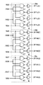
図13は、図10に示す本発明の実施の形態4におけるMWLドライバの構成の一例を示す図であり、代表例として、1のメモリブロックに対応するMWLドライバの構成を示す。なお、参考のため、MWLプリデコーダ22dを併せて示している。
【0160】
MWLプリデコーダ22dの基本構成は、MWLプリデコーダ22cと同じである。MWLプリデコーダ22dは、アドレス信号RA3〜RA8に応答して、プリデコード信号XF1L(0)〜XF1L(3)、プリデコード信号XF1M(0)〜XF1M(3)、プリデコード信号XF1H(0)〜XF1H(3)を出力する。
【0161】
図13に示すMWLドライバは、NAND回路N25.0、…、N25.63、レベル変換回路S6.0、…、S6.63、およびインバータI16.0、…、I16.63を含む。NAND回路N25.0、…、N25.63、レベル変換回路S6.0、…、S6.63、およびインバータI16.0、…、I16.63のそれぞれは、ノーマルブロックにおけるメインワード線に対応して配置する。
【0162】
たとえば、NAND回路N25.0は、MWLプリデコーダ22dから対応するプリデコード信号XF1L(0)〜XF1L(3)、XF1H(0)〜XF1H(3)、XF1M(0)〜XF1M(3)を受ける。インバータI16.0は、対応するレベル変換回路S6.0を介して、NAND回路N25.0の出力を受け、対応するメインワード線選択信号/MWL(0)を出力する。
【0163】
図13に示すMWLドライバはさらに、レベル変換回路S7.0、…、S7.kおよびインバータI17.0、…、I17.kを含む。レベル変換回路S7.0、…、S7.kおよびインバータI17.0、…、I17.kのそれぞれは、冗長メインワード線RMWL(0)、…、RMWL(k)のそれぞれに対応して配置する。
【0164】
たとえば、レベル変換回路S7.0は、冗長判定回路46の出力する信号RMWL(0)を受ける。インバータI17.0は、対応するレベル変換回路S7.0の出力を反転して、対応する冗長メインワード線選択信号/RMWL(0)を出力する。
【0165】
図14は、図10に示す本発明の実施の形態4におけるS/A帯制御信号ドライバの構成を示す図である。図14に示す構成は、図10におけるSDドライバ・S/A帯制御信号ドライバ42に含まれる。
【0166】
図14に示すS/A帯制御信号ドライバは、NAND回路N26、レベル変換回路S8aおよびS8b、ならびにインバータI17aおよびI17bを含む。
【0167】
インバータI17aは、対応するブロック選択信号BS(i)を反転して出力する。インバータI17bは、隣接するメモリブロックに対応するブロック選択信号BS(i+1)を反転して出力する。NAND回路N26は、インバータI17aおよびI17bの出力を受ける。NAND回路N26から対応するイコライズ信号BLEQが出力される。
【0168】
レベル変換回路S8aは、インバータI17aの出力を受けて、一方のシェアードゲート信号SHR(U)を出力する。レベル変換回路S8bは、インバータI17bの出力を受けて、他方のシェアードゲート信号SHR(D)を出力する。メモリブロックが選択されると、冗長判定の有無に関わらず、非選択のメモリブロック側を分離するシェアードゲート信号、およびビット線対をイコライズするイコライズ信号BLEQを非活性化する。
【0169】
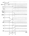
次に、本発明の実施の形態4における半導体記憶装置の動作について、タイミングチャートである図15を参照して説明する。
【0170】
図15は、本発明の実施の形態4における半導体記憶装置1400の動作を説明するためのタイミングチャートである。
【0171】
外部制御信号に応答して、アクト信号ACTがHレベルの活性状態になり、ロウアドレス信号が取込まれる。この時点で、判定信号RHITおよびRMISは、ともにLレベルの状態にある。
【0172】
冗長ブロックを有しないメモリブロック1.2が選択されたとする。時刻t0においてアクト信号ACTにより、ロウ系がアクティブになると同時(時刻t0)に、対応するサブデコード信号SDおよび/SDが活性化、シェアードゲート信号SHRおよびイコライズ信号BLEQが非活性化する。冗長ブロックについても、対応する冗長サブデコード信号RSDおよび/RSDが活性化、シェアードゲート信号SHRおよびイコライズ信号BLEQが非活性化する。
【0173】
時刻t0〜t1において、冗長判定回路46が、冗長使用/未使用の判定処理を行う。時刻t1において、判定結果として、判定信号RHIT、RMIS、および冗長メインワード線選択信号/RMWL(0)〜(k)が出力される。
【0174】
冗長メインワード線選択信号は、対応する冗長メインワード線を選択状態にする信号であって、初期状態においては、すべてLレベルの状態にある。
【0175】
冗長未使用の場合には、判定信号RMISがHレベル(実線部分)になる。判定信号RMISがHレベルに立上がることにより、メモリブロック1.0および1.15の選択が解除され、活性状態のサブデコード信号SDおよび/SDが非活性化される。シェアードゲート信号SHRおよびイコライズ信号BLEQは、非活性となる。
【0176】
また、判定信号RMISがHレベルに立上がることにより、MWLプリデコード22dから出力されるプリデコード信号のいずれか1つがLレベルからHレベルに立上がる。これにより、対応するメインワード線選択信号が活性化し、ノーマルブロックのワード線WLが選択状態となる。
【0177】
冗長使用の場合には、判定信号RHITがHレベル(点線部分)になる。置換先の冗長メインワード線選択信号が活性化(Hレベル)される。
【0178】
判定信号RHITがHレベルに立上がることにより、ロウアドレスにより選択されていたメモリブロック1.2が非選択化される。これと同時に1つの冗長メインワード線選択信号が活性化される。対応するスペアワード線SWLが選択状態になる。
【0179】
このように、時刻t0〜t1の判定処理期間τ0に、ノーマルブロックについてのサブデコード信号SDの活性化、およびセンスアンプの活性化を制御するシェアードゲート信号等を非活性化することにより、続く時刻t1〜t2の期間τ1では、メインワード線の立下げと、ワード線の立上げを行うだけでよいため、ワード線を立上げに要する時間を短縮することが可能となる。
【0180】
図16は、本発明の実施の形態4における置換を示す図である。図16に示すように、半導体記憶装置1400においては、ノーマルブロックNBL(0)〜NBL(7)に対しては、メモリブロック1.15に位置する冗長ブロック40bを使用し、ノーマルブロックNBL(8)〜NBL(15)に対しては、メモリブロック1.0に位置する冗長ブロック40aを使用する。これは、隣合うメモリブロックへ置換した場合、2つのメモリブロック間に挟まれたセンスアンプブロックのシェアードゲート信号SHRを一旦非活性化し、冗長判定後のワード線の立上げまでにもう一度活性化する必要が生じるためである。これによると、ワード線の立上げに時間を要するからである。
【0181】
なお、本発明は、図16に示す置換に限られず、図17および図18に示す構成で置換を行っても同様の効果が得られる。
【0182】
図17および図18は、本発明の実施の形態4における他の置換の例を示す図である。図17に示す構成では、奇数番目のノーマルブロックNBL(1)、NBL(3)、…については、冗長ブロック40aを用いて置換する。偶数番目のノーマルブロックNBL(0)、NBL(2)、…については、冗長ブロック40bを用いて置換する。
【0183】
また、図18に示す構成では、1つの冗長ブロック40aに対して専用のセンスアンプブロックを備える。全てのノーマルブロックNBL(0)、NBL(1)、…について、冗長ブロック40aを用いて置換する。この場合であっても、アドレス信号の入力とともに、センスアンプに対する信号を制御することにより、高速アクセスが可能となる。
【0184】
なお、階層ワード線構成でない場合であっても、本発明は適用可能であり、アクセスの高速化が図れる。
【0185】
[実施の形態5]
本発明の実施の形態5における半導体記憶装置について説明する。本発明の実施の形態5は、冗長セルが物理的に救済範囲内に分散して存在する半導体記憶装置において、サブデコード信号(正規および冗長)を一括して活性化し、冗長判定後に活性化したサブデコード信号のなかから必要な信号を選択することにより、高速アクセスを図るものである。
【0186】
本発明の実施の形態5における半導体記憶装置について図19を用いて説明する。図19は、本発明の実施の形態5における半導体記憶装置1500の主要部の構成の一例を示す図である。半導体記憶装置1000〜1400と同じ構成要素には、同じ符号および同じ符号を付し、その説明を省略する。
【0187】
図19に示す半導体記憶装置は、冗長救済範囲REDにおいて、冗長メインワード線RMWLが分散して存在する。複数のセンスアンプS/Aから構成されるセンスアンプ列により区切られたブロック毎に、1本の冗長メインワード線RMWLを配置する。ノーマルブロックに対するサブデコード信号を伝送するサブデコード線SD0、SD1、…と冗長ブロックに対するサブデコード信号を伝送する冗長サブデコード線RSD0、RSD1、…とを平行に配置する。
【0188】
ノーマルブロックにおけるサブデコード線(たとえば、SD1およびSD2)に対して、置換する可能性のある全ての冗長サブデコード線RSD1、…、RSD4を同時に活性化する。
【0189】
図20は、図19における半導体記憶装置1500の要部の構成を示す図である。図3に示す構成と同じ構成要素には、同じ記号および符号を付し、その説明を省略する。
【0190】
図20における構成では、図3に示す冗長判定回路20に代わって、冗長判定回路50を備える。冗長判定回路50は、アドレス信号に応答して、対応するブロックを指定する16ビットの信号RSDRST(0)、…、RSDRST(15)を出力する。MWLデコーダ25.nは、プリデコード信号RSDF(0)、…、RSDF(15)に代わって、プリデコード信号RSDRST(0)、…、RSDRST(15)を受ける。
【0191】
16ビットの信号RSDRST(0)、…、RSDRST(15)は、冗長判定前は、すべてHレベルである。いずれかのプリデコード信号XF0が活性化されると、対応する冗長サブデコード線RSD0〜RSD15が活性化する。
【0192】
冗長判定後、信号RSDRST(0)、…、RSDRST(15)のいずれか1つを残して、他の信号(非選択)がLレベルになる。
【0193】
次に、本発明の実施の形態5における半導体記憶装置の動作について、タイミングチャートである図21および図22を参照して説明する。図21および図22は、図19に示す本発明の実施の形態5における半導体記憶装置1500の動作を説明するためのタイミングチャートである。
【0194】
ロウアクセス時、アドレス信号RA0〜RA12に応答して、置換可能性のある全ての冗長サブデコード信号を活性化する。
【0195】
具体的には、ノーマルブロックにおけるサブデコード線(図19におけるSD1およびSD2)と、冗長救済範囲内REDにある全ての冗長サブデコード線(図19におけるRSD1、…、RSD4、…)とを活性化する。
【0196】
冗長判定後、対応する冗長サブデコード信号またはサブデコード信号の一方のみを残し、他を非活性化する。この結果、ノーマルブロックまたは冗長ブロックにおけるいずれか一方のワード線が活性化(図21における記号a)し、他方のワード線が非活性化(図21における記号b)する。
【0197】
サブデコード信号の活性化の過程で、冗長判定を行わない。このため、アクセス速度は、冗長救済範囲REDが、センスアンプブロックで区切られたブロック内に限定される場合と同じである。
【0198】
[実施の形態6]
本発明の実施の形態6における半導体記憶装置について説明する。本発明の実施の形態6における半導体記憶装置は、冗長判定前にサブデコード信号(ノーマルブロックおよび冗長ブロック)を中間電位まで立上げておくことにより、アクセス時間の短縮を図るものである。
【0199】
本発明の実施の形態6における半導体記憶装置の主要部の構成について、図23を用いて説明する。図23は、本発明の実施の形態6における半導体記憶装置1600の主要部の構成の一例を示す図である。
【0200】
図23に示す半導体記憶装置1600は、複数のメモリブロックに分割されるメモリセルアレイ65、入力バッファ61、プリデコーダ62および64、ドライバ63、および冗長判定回路60を含む。
【0201】
入力バッファ61は、外部から外部アドレス信号を取込む。冗長判定回路60は、入力バッファ61から受けるアドレス信号に基づき、冗長判定を行う。判定結果として、判定信号HITおよびMISSを出力する。
【0202】
プリデコーダ62は、入力バッファ61から受けるアドレス信号に基づき、リセット信号RST0、…を出力する。プリデコーダ64は、入力バッファ61から受けるアドレス信号をデコードする。ドライバ63は、プリデコーダ64の出力するデコード信号に基づき、メモリセルアレイ65のワード線またはスペアワード線を選択状態とする。
【0203】
図24は、図23に示す本発明の実施の形態6におけるメモリセルアレイ65の構成を示す図である。図24に示すようにメモリセルアレイ65は、ノーマルブロックB0、…、B3のそれぞれに対して、冗長ブロックS0、…、S3を配置する。ノーマルブロックと冗長ブロックとに対して、センスアンプブロック66を配置する。半導体記憶装置1600は、階層ワード線方式の構成を備える。
【0204】
図25は、図23に示す本発明の実施の形態6におけるノーマルブロックに対する回路構成を示す図であり、図26は、図23に示す本発明の実施の形態6における冗長ブロックに対する回路構成を示す図である。本発明の実施の形態6においては、ノーマルブロックと冗長ブロックとでサブデコード信号を伝送する伝送線を分割する。
【0205】
図25を参照して、ノーマルブロックでは、1本のメインワード線MWLに対して、4本のワード線SWLを配置する。4本のワード線SWLのいずれか1本を選択するためのサブデコード信号を伝送する信号線として、サブデコード線SD0、SD1、SD2およびSD3を配置する。
【0206】
各サブデコード線に対して、PMOSトランジスタPT30およびPT32、ならびにNMOSトランジスタNT30およびNT32を配置する。PMOSトランジスタPT30およびNMOSトランジスタNT30は、中間電位VCCと接地電位との間に直列に接続される。PMOSトランジスタPT32およびNMOSトランジスタNT32は、電源電位VPPと接地電位との間に直列に接続される。
【0207】
PMOSトランジスタPT30とNMOSトランジスタNT30との接続ノード、およびPMOSトランジスタPT32とNMOSトランジスタNT32との接続ノードは、対応するサブデコード線と接続される。
【0208】
PMOSトランジスタPT32のゲート電極は、判定信号MISSを反転した信号/MISSを受ける。NMOSトランジスタNT32のゲート電極は、判定信号HITを受ける。
【0209】
サブデコード線SD0、SD1、SD2、SD3のそれぞれのNMOSトランジスタNT30のゲート電極に対して、リセット信号RST0、RST1、RST2、RST3がそれぞれ与えられる。
【0210】
サブデコード線SD0、SD1、SD2、SD3のそれぞれのPMOSトランジスタPT30のゲート電極に対して、プリチャージ信号/PC0、/PC1、/PC2、/PC3がそれぞれ与えられる。
【0211】
図26を参照して、冗長ブロックでは、1本の冗長メインワード線SMWLに対して、4本のスペアワード線SSWLを配置する。4本のスペアワード線SSWLのいずれか1本を選択するための冗長サブデコード信号を伝送する信号線として、冗長サブデコード線SSD0、SSD1、SSD2およびSSD3を配置する。
【0212】
各冗長サブデコード線に対して、PMOSトランジスタPT34およびPT36、ならびにNMOSトランジスタNT34およびNT36を配置する。PMOSトランジスタPT34およびNMOSトランジスタNT34は、中間電位VCCと接地電位との間に直列に接続される。PMOSトランジスタPT36およびNMOSトランジスタNT36は、電源電位VPPと接地電位との間に直列に接続される。
【0213】
PMOSトランジスタPT34とNMOSトランジスタNT34との接続ノード、およびPMOSトランジスタPT36とNMOSトランジスタNT36との接続ノードは、対応する冗長サブデコード線と接続される。
【0214】
PMOSトランジスタPT36のゲート電極は、判定信号HITを反転した信号/HITを受ける。NMOSトランジスタNT36のゲート電極は、判定信号MISSを受ける。
【0215】
冗長サブデコード線SSD0、SSD1、SSD2、SSD3のそれぞれのNMOSトランジスタNT34のゲート電極に対して、リセット信号RST0、RST1、RST2、RST3がそれぞれ与えられる。
【0216】
冗長サブデコード線SSD0、SSD1、SSD2、SSD3のそれぞれのPMOSトランジスタPT34のゲート電極に対して、プリチャージ信号/PC0、/PC1、/PC2、/PC3がそれぞれ与えられる。
【0217】
バンク活性信号が入力されると、入力したアドレス信号(上位)をデコードした信号に基づき、対応するワード線SWLおよびスペアワード線SSWLに関するサブデコード線および冗長サブデコード線を同時に活性化する。この時点での活性化レベルを中間電位VCCに設定する。
【0218】
冗長判定の結果が出された時点で、ノーマルブロックのサブデコード線を活性化するか、冗長ブロックの冗長サブデコード線を活性化するかを選択する。選択されたサブデコード線(冗長サブデコード線)については、電源電位VPPレベルにまで電圧レベルを上げる。非選択のサブデコード線(冗長サブデコード線)については、非活性化させる。
【0219】
次に、本発明の実施の形態6における半導体記憶装置1600の動作について、タイミングチャートである図27を参照して説明する。
【0220】
図27は、本発明の実施の形態6における半導体記憶装置1600の動作を説明するためのタイミングチャートである。半導体記憶装置1600は、内部クロック信号CLKに同期して動作する。アドレス信号に対して、サブデコード線SD0が選択されるものとする。
【0221】
あるバンクBK0に対するアクト信号ACT0が入力されると、フラグBAflag0が活性化される。バンクBK0に対応するプリチャージ信号/PC(B0)が一時的に活性化する。バンクBK0に対応するリセット信号RST0(B0)が非活性化する。このフラグBAflag0に基づき、アドレス信号に対応して、サブデコード線SD0および冗長サブデコード線SSD0がプリチャージされる。
【0222】
ここで、選択されるノーマルブロックのメモリセルが正常である場合、判定信号MISSが活性化される。これにより、サブデコード線SD0の電位が、電源電位VPPレベルにまで上昇する。冗長サブデコード線SSD0の電位は、接地電位レベルにまで低下する。
【0223】
その後、対応するメインワード線MWLが活性化されることにより、選択されたワード線SWLが選択状態となる。この状態は、バンクの活性化をリセットする信号BankRST0の入力まで保持される。
【0224】
バンクBK1に対するアクト信号ACT1が入力されると、フラグBAflag1が活性化される。バンクBK1に対応するプリチャージ信号/PC(B1)が一時的に活性化する。バンクBK1に対応するリセット信号RST0(B1)が非活性化する。このフラグBAflag1に基づき、アドレス信号に対応して、サブデコード線SD0および冗長サブデコード線SSD0がプリチャージされる。
【0225】
ここで、選択されるノーマルブロックのメモリセルが不良である場合、判定信号HIT(B1)が活性化される。これにより、冗長サブデコード線SSD0の電位が、電源電位VPPレベルにまで上昇する。サブデコード線SD0の電位は、接地電位レベルにまで低下する。
【0226】
その後、対応する冗長メインワード線SMWLが活性化されることにより、選択されたスペアード線SSWLが選択状態となる。この状態は、バンクの活性化をリセットする信号BankRST1の入力まで保持される。
【0227】
このように、上位のアドレス信号をデコードした結果を用いることで、冗長判定に関係なく、サブデコード線および冗長サブデコード線を高速に中間レベルにまで活性化できる。
【0228】
そして、中間電位にまで活性化させておくことで、冗長判定の結果を用いて、高速にワード線を選択することが可能となる。
【0229】
なお、電源電位VPPのような高電位を使用することなく、活性レベルを中間電位VCCとすることで、消費電力を抑えることが可能となる。また、電源電位を発生させる回路の負担を軽減することが可能となる。
【0230】
[実施の形態7]
本発明の実施の形態7における半導体記憶装置について説明する。本発明の実施の形態7における半導体記憶装置は、複数のノーマルブロックを含むバンク毎に専用の冗長ブロックを配置することにより、救済効率の向上を図るものである。
【0231】
図28は、本発明の実施の形態7における半導体記憶装置1700のメモリマットの構成を示す図である。図28に示すメモリマットは、2つのバンクB0およびB1を配置する。
【0232】
バンクB0およびB1はそれぞれ、正規のメモリセルから構成されるノーマルブロックNBL(0)、…、NBL(m)を含み、シェアードセンスアンプ方式の構成(センスアンプブロック70)をとる。
【0233】
さらに、バンクB0およびB1はそれぞれ、冗長セルから構成される冗長ブロックRBL(0)および冗長ブロックRBL(1)を含む。冗長ブロックRBL(0)および冗長ブロックRBL(1)は、ともにシェアードセンスアンプ方式の構成(センスアンプブロック70)をとる。
【0234】
バンクB0におけるノーマルブロックに対しては、同一バンクにおける冗長ブロックRBL(0)を用いて置換を行なう。バンクB1におけるノーマルブロックに対しては、同一バンクにおける冗長ブロックRBL(1)を用いて置換を行なう。
【0235】
バンクB0およびB1は、内部クロック信号に応答して動作し、しかも互いに独立して動作することが可能である。
このように、バンクの各々に対して独立して冗長ブロックを配置することにより、高速な救済が可能となる。
【0236】
[実施の形態8]
本発明の実施の形態8における半導体記憶装置について説明する。本発明の実施の形態8における半導体記憶装置は、実施の形態7における半導体記憶装置に対して、センスアンプの共有化を図ることにより、救済効率の向上およびレイアウト面積の削減を図るものである。
【0237】
図29は、本発明の実施の形態8における半導体記憶装置1800のメモリマットの構成を示す図である。図28に示す構成と同じ部分には、同じ記号を付しその説明を省略する。
【0238】
図29に示すメモリマットは、2つのバンクB0およびB1を含む。バンクB0におけるノーマルブロックNBL(0)、…、NBL(m)、ならびに冗長ブロックRBL(0)は、シェアードセンスアンプ方式の構成(センスアンプブロック70)をとる。バンクB1におけるノーマルブロックNBL(0)、…、NBL(m)、ならびに冗長ブロックRBL(1)は、シェアードセンスアンプ方式の構成(センスアンプブロック70)をとる。
【0239】
バンクB0に対応する冗長ブロックRBL(0)と、同じバンクB0に属するノーマルブロックNBL(0)とで、センスアンプブロック70を共有する。
【0240】
バンクB1に対応する冗長ブロックRBL(1)と、同じバンクB0に属するノーマルブロックNBL(m)とで、センスアンプブロック70を共有する。
【0241】
このように構成することにより、高速な救済が可能となるとともに、レイアウト面積を削減することが可能となる。
【0242】
[実施の形態9]
本発明の実施の形態9における半導体記憶装置について説明する。本発明の実施の形態9における半導体記憶装置は、実施の形態8における半導体記憶装置に対して、図30に示す構成をとる。
【0243】
図30は、本発明の実施の形態9における半導体記憶装置1900のメモリマットの構成を示す図である。図29に示す構成と同じ部分には、同じ記号を付しその説明を省略する。
【0244】
図30に示すメモリマットは、2つのバンクB0およびB1を含む。バンクB0におけるノーマルブロックNBL(0)、…、NBL(m)、ならびに冗長ブロックRBL(0)は、シェアードセンスアンプ方式の構成(センスアンプブロック70)をとる。バンクB1におけるノーマルブロックNBL(0)、…、NBL(m)、ならびに冗長ブロックRBL(1)は、シェアードセンスアンプ方式の構成(センスアンプブロック70)をとる。
【0245】
冗長ブロックRBL(0)およびRBL(1)は、バンクB0とB1とで挟まれる領域に配置する。
【0246】
バンクB0に対応する冗長ブロックRBL(0)と、同じバンクB0に属するノーマルブロックNBL(m)とで、センスアンプブロック70を共有する。
【0247】
バンクB1に対応する冗長ブロックRBL(1)と、同じバンクB0に属するノーマルブロックNBL(0)とで、センスアンプブロック70を共有する。
【0248】
このように構成することにより、高速な救済が可能となるとともに、レイアウト面積を削減することが可能となる。
【0249】
[実施の形態10]
本発明の実施の形態10における半導体記憶装置について説明する。
【0250】
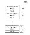
図31は、本発明の実施の形態10における半導体記憶装置2000のメモリマットの構成を示す図である。図30に示す構成と同じ部分には、同じ記号を付しその説明を省略する。
【0251】
図31に示すメモリマットは、2以上の複数のバンクB0、…、Bnを含む。各バンクは、ノーマルブロック(図中記号NBL(0)、NBL(1)、…)と冗長ブロック(図中記号RBL(0)、RBL(1)、…)とを備える。各バンクにおける冗長ブロックは、同一のブロックに属するノーマルブロックを置換するために用いる。各バンクは、内部クロック信号に応答して独立に動作する。このように構成することにより、高速な救済が可能となる。
【0252】
【発明の効果】
請求項1に係る半導体記憶装置によれば、異なるメモリブロックにおける冗ブロックを用いて置換可能な半導体記憶装置において、冗長使用の判定処理と独立して、ワード線および冗長ワード線を選択状態とするために必要な制御(信号発生)を行なうことにより、高速なアクセスが可能となる。
【0256】
請求項2および請求項7に係る半導体記憶装置は、請求項1に係る半導体記憶装置であって、冗長使用の判定処理と独立して、ワード線および冗長ワード線を選択状態とするために必要な活性化信号を活性化し、さらに冗長判定後に必要な信号を残して非活性化させる。これにより、冗長未使用の場合、高速なアクセスが可能となる。
【0257】
請求項3、請求項4および請求項8に係る半導体記憶装置は、請求項1に係る半導体記憶装置であって、冗長判定の判定処理と独立して、対応するセンスアンプについての制御信号を発生しておく。また冗長使用の判定処理と独立して、ワード線および冗長ワード線を選択状態とするために必要な活性化信号を活性化し、さらに冗長判定後に必要な信号を残して非活性化させる。これにより、高速アクセスが可能となる。
【0258】
請求項5および請求項6に係る半導体記憶装置は、請求項1に係る半導体記憶装置であって、冗長使用の判定処理と独立して、ワード線および冗長ワード線を選択状態とするために必要な活性化信号を中間レベルに立上げ、さらに冗長判定後に必要な信号を活性化し、他の信号を非活性化させる。これにより、冗長未使用の場合、高速なアクセスが可能となる。また、中間レベルの電源電圧を使用するため、周辺回路への負担を抑え、消費電力を低減させることができる。
【0259】
請求項9に係る半導体記憶装置は、冗長ブロックを有する半導体記憶装置において、冗長使用の判定処理と独立して、ワード線および冗長ワード線を選択状態とするために必要な活性化信号を中間レベルに立上げ、さらに冗長判定後に必要な信号を活性化し、他の信号を非活性化させる。これにより、冗長未使用の場合、高速なアクセスが可能となる。
【0260】
請求項10および請求項11に係る半導体記憶装置は、請求項9に係る半導体記憶装置であって、中間レベルの電源電圧を使用するため、周辺回路への負担を抑え、消費電力を低減させることができる。
【0261】
請求項12に係る半導体記憶装置は、請求項11に係る半導体記憶装置であって、冗長判定のタイミングでなく、デコードのタイミングで必要な信号を活性化させることが可能となる。
【図面の簡単な説明】
【図1】 本発明の実施の形態1における半導体記憶装置1000の全体構成を示す図である。
【図2】 図1に示す本発明の実施の形態1におけるWLドライバ4の構成を示す図である。
【図3】 図1に示す本発明の実施の形態1におけるロウアドレス系デコード回路21の主要部の構成を示す図である。
【図4】 図3に示す本発明の実施の形態1におけるMWLプリデコーダ22cの構成を示す図である。
【図5】 本発明の実施の形態1におけるMWLドライバの構成を示す図である。
【図6】 本発明の実施の形態1における半導体記憶装置1000の動作を説明するためのタイミングチャートである。
【図7】 本発明の実施の形態2における半導体記憶装置1200の主要部の構成の一例を示す図である。
【図8】 図7に示す本発明の実施の形態2におけるSDローカルドライバの構成の一例を示す図である。
【図9】 本発明の実施の形態3におけるSDローカルドライバの構成の一例を示す図である。
【図10】 本発明の実施の形態4における半導体記憶装置1400の全体構成の一例を示す図である。
【図11】 図10に示す本発明の実施の形態4におけるブロック選択回路45の構成の一例を示す図である。
【図12】 図10に示す本発明の実施の形態4におけるSDドライバの構成の一例を示す図である。
【図13】 図10に示す本発明の実施の形態4におけるMWLドライバの構成の一例を示す図である。
【図14】 図10に示す本発明の実施の形態4におけるS/A帯制御信号ドライバの構成を示す図である。
【図15】 本発明の実施の形態4における半導体記憶装置1400の動作を説明するためのタイミングチャートである。
【図16】 本発明の実施の形態4における置換を示す図である。
【図17】 本発明の実施の形態4における他の置換の例を示す図である。
【図18】 本発明の実施の形態4における他の置換の例を示す図である。
【図19】 本発明の実施の形態5における半導体記憶装置1500の主要部の構成の一例を示す図である。
【図20】 図19における半導体記憶装置1500の要部の構成を示す図である。
【図21】 図19に示す本発明の実施の形態5における半導体記憶装置1500の動作を説明するためのタイミングチャートである。
【図22】 図19に示す本発明の実施の形態5における半導体記憶装置1500の動作を説明するためのタイミングチャートである。
【図23】 本発明の実施の形態6における半導体記憶装置1600の主要部の構成の一例を示す図である。
【図24】 図23に示す本発明の実施の形態6におけるメモリセルアレイ65の構成を示す図である。
【図25】 図23に示す本発明の実施の形態6におけるノーマルブロックに対する回路構成を示す図である。
【図26】 図23に示す本発明の実施の形態6における冗長ブロックに対する回路構成を示す図である。
【図27】 本発明の実施の形態6における半導体記憶装置1600の動作を説明するためのタイミングチャートである。
【図28】 本発明の実施の形態7における半導体記憶装置1700のメモリマットの構成を示す図である。
【図29】 本発明の実施の形態8における半導体記憶装置1800のメモリマットの構成を示す図である。
【図30】 本発明の実施の形態9における半導体記憶装置1900のメモリマットの構成を示す図である。
【図31】 本発明の実施の形態10における半導体記憶装置2000のメモリマットの構成を示す図である。
【図32】 従来の半導体記憶装置9000における全体構成を示す図である。
【図33】 図32に示す従来の半導体記憶装置におけるWLドライバ914の構成を示す図である。
【図34】 図32に示す従来の半導体記憶装置9000における動作を説明するためのタイミングチャートである。
【符号の説明】
1 メモリブロック、2,66,70 センスアンプブロック、4,63 ドライバ、21 ロウアドレス系デコード回路、20,46,50,60 冗長判定回路、22,33 ロウプリデコーダ、23,45 ブロック選択回路、24SDドライバ/SAドライバ、25 MWLドライバ、31 MWLデコーダ/ドライバ、32a, 32b,36a,36b SDローカルドライバ、34ブロック選択回路/SDドライバ、901 レジスタ、902 ロウアドレスバッファ、42 SDドライバ・S/A帯制御信号ドライバ、61 入力バッファ、62,64 プリデコーダ、40a,40b,RBL 冗長ブロック、NBLノーマルブロック、1000〜1900 半導体記憶装置。[0001]
BACKGROUND OF THE INVENTION
The present invention relates to a semiconductor memory device, and more particularly to a semiconductor memory device including a replaceable redundant cell.
[0002]
[Prior art]
An example of a semiconductor memory device having a conventional redundant cell will be briefly described with reference to FIG.
[0003]
FIG. 32 is a diagram showing an overall configuration of a conventional
[0004]
The
[0005]
The
[0006]
The
[0007]
In response to the enable signal PDE output from the
[0008]
Data input /
[0009]
An SD driver / SA driver 924 and an
[0010]
The
[0011]
A
[0012]
FIG. 33 is a diagram showing a configuration of
[0013]
Memory block 1.1 includes a plurality of redundant and normal memory cells MC, a plurality of bit line pairs BL (0) and / BL (0),..., A plurality of word lines WL (n), WL (n + 1),. A plurality of spare word lines SWL (0), SWL (1),. The plurality of bit line pairs are arranged corresponding to each column. A plurality of word lines and spare word lines are arranged corresponding to each row.
[0014]
Sense amplifier blocks (
[0015]
[0016]
The
[0017]
[Problems to be solved by the invention]
By the way, the memory cell array in which the redundant region is arranged has an essential configuration for the semiconductor memory device. In this regard, in particular, the conventional
[0018]
However, in general, in a semiconductor memory device including redundant cells, there is a problem that a block to be activated is not determined until redundancy is determined, and high-speed access is insufficient.
[0019]
This problem will be described with reference to FIG. 34 using the conventional semiconductor memory device shown in FIG. 32 as a specific example. FIG. 34 is a timing chart for explaining the operation of conventional
[0020]
Referring to FIG. 34, a row-related operation is started by bank activation signal ACT. Address signals RA0-RA12 are latched, and a word line or spare word line is selected and a sense amplifier is activated. When the word line is selected, the redundant use / non-use determination is performed.
[0021]
At time t0, the row address reaches the
[0022]
Specifically, when the memory block 1.1 is selected, the sense amplifier blocks located at both ends thereof are activated. In preparation for the operation, the equalize signal BLEQ is set to L level to release the equalization of the bit line, and the shared gates SHR (U) and SHE (D) are set to L level to turn off the shared gate. These operations are completed before the word line is raised after the redundancy determination.
[0023]
As a result, τ0 + τ20 (where τ20 = t2−t0) is finally required from the input of the row address to the rise of the word line.
[0024]
As a further problem, there is a problem that the layout area increases when redundant cells are used.
[0025]
Accordingly, the present invention has been made to solve such a problem, and an object thereof is to provide a semiconductor memory device capable of high-speed operation in a semiconductor memory device having redundant cells.
[0026]
Another object of the present invention is to provide a semiconductor memory device with high relief efficiency while suppressing the layout area.
[0027]
[Means for Solving the Problems]
The semiconductor memory device according to
[0033]
Claim2A semiconductor memory device according to claim1The first control means includes a first signal generating means for generating a word line activation signal for activating a word line corresponding to the external address signal, and a plurality of normal blocks. And a plurality of normal cell selecting means for selecting the corresponding word line in response to a corresponding word line activation signal, and a second control means. Corresponds to a second signal generating means for generating a redundant word line activation signal for activating a redundant word line corresponding to the external address signal, and a plurality of redundant word lines in a plurality of redundant blocks, respectively. A plurality of redundant cell selecting means for selecting a corresponding redundant word line in response to a corresponding redundant word line activation signal, wherein the first signal generating means The activated word line activation signal is deactivated in response to the result of redundancy determination received from the second signal generating means, and the second signal generating means is activated in response to the redundancy undetermined result received from the determining means. The word line activation signal is deactivated.
[0034]
Claim3A semiconductor memory device according to claim1And a plurality of sense amplifier blocks provided corresponding to each of the plurality of memory blocks and the plurality of redundant blocks, each of the plurality of sense amplifier blocks including a plurality of sense amplifier means. Each of the plurality of sense amplifier means includes means for amplifying the potential of the corresponding bit line, an equalizing circuit for equalizing the potential of the corresponding bit line, and a bit line corresponding to the non-selected memory block side. And an S / A share circuit that generates a first control signal for controlling the activation of the sense amplifier block in the corresponding normal block in response to the external address signal, and a second control signal. The control means controls the activation of the sense amplifier block in the corresponding redundant block in response to the external address signal. The first signal generating means changes the level of the generated first control signal in response to the result of the redundancy judgment received from the judging means, and the second signal generating means Changes the level of the generated second control signal in response to the redundancy undetermined result received from the determining means.
[0035]
Claim4A semiconductor memory device according to claim3The first control means includes a first signal generating means for generating a word line activation signal for activating a word line corresponding to the external address signal, and a plurality of normal blocks. And a plurality of normal cell selecting means provided corresponding to each of the plurality of word lines and selecting the corresponding word line in response to the corresponding word line activation signal. The means corresponds to a second signal generating means for generating a redundant word line activation signal for activating a redundant word line corresponding to the external address signal, and a plurality of redundant word lines in a plurality of redundant blocks, respectively. A plurality of redundant cell selecting means for selecting a corresponding redundant word line in response to a corresponding redundant word line activation signal, and generating a first signal The stage deactivates the activated word line activation signal in response to the result of the redundancy determination received from the determination means, and the second signal generation means responds to the redundancy undetermined result received from the determination means. Then, the activated redundant word line activation signal is deactivated.
[0036]
Claim5A semiconductor memory device according to claim1A first signal generating means for generating a first level word line activation signal for activating a word line corresponding to an external address signal; In response to the redundant unused determination result received from the redundant means, the means for raising the level of the first level word line activation signal to the active level and each of the plurality of word lines in the plurality of normal blocks A plurality of normal cell selecting means for selecting the corresponding word line in response to a corresponding word line activation signal, wherein the second control means is a redundant word line corresponding to the external address signal. Second signal generating means for generating a first-level redundant word line activation signal for activating the first-level redundant word in response to the redundant use determination result received from the redundant means Means for raising the level of the activation signal to the activation level and a corresponding redundant word provided corresponding to each of the plurality of redundant word lines in the plurality of redundant blocks and in response to the corresponding redundant word line activation signal A plurality of redundant cell selecting means for selecting a line, wherein the first signal generating means deactivates the activated word line activation signal in response to the result of the redundancy judgment received from the judging means, The second signal generating means inactivates the activated redundant word line activation signal in response to the redundancy undetermined result received from the determining means.
[0037]
Claim6A semiconductor memory device according to claim5The first level is a substantially intermediate value between the active level and the inactive level.
[0038]
Claim7A semiconductor memory device according to claim2Each of the plurality of word lines includes a main word line and a plurality of sub word lines provided corresponding to each of the main word lines, and each of the plurality of redundant word lines includes A redundant main word line and a plurality of spare word lines provided corresponding to each of the redundant main word lines, the word line activation signal selects a sub word line, and the redundant word line activation signal is spare The word line is selected.
[0039]
Claim8A semiconductor memory device according to claim4Each of the plurality of word lines includes a main word line and a plurality of sub word lines provided corresponding to each of the main word lines, and each of the plurality of redundant word lines includes A redundant main word line and a plurality of spare word lines provided corresponding to each of the redundant main word lines, the word line activation signal selects a sub word line, and the redundant word line activation signal is spare The word line is selected.
[0040]
Claim9The semiconductor memory device according to the present invention includes a plurality of normal memory cells arranged in a matrix, a plurality of word lines arranged corresponding to rows, and a plurality of bit lines arranged corresponding to columns. A normal block, a plurality of redundant cells arranged in a matrix and replaced with corresponding normal memory cells, a plurality of redundant word lines arranged corresponding to rows, and arranged corresponding to columns A redundant block including a plurality of bit lines, a determination unit that determines whether or not redundancy is used in response to an external address signal, and a response in response to an external address signal independently of the determination result of the determination unit First control means for controlling the selected word line to be selected, and for selecting the corresponding redundant word line in response to the external address signal independently of the determination result of the determining means. Second control means for controlling The first control means receives the result of the redundancy determination by the determination means and performs control for bringing the corresponding word line into a non-selected state, and the second control means performs redundancy not determined by the determination means. In response to the result of use determination, control is performed to put the corresponding redundant word line into a non-selected state.
[0041]
Claim10A semiconductor memory device according to claim9A first signal generating means for generating a first level word line activation signal for activating a word line corresponding to an external address signal; In response to the determination result of redundancy unused received from the redundancy means, a means for raising the level of the first level word line activation signal to the activation level and a plurality of word lines are provided correspondingly. A plurality of normal cell selecting means for selecting the corresponding word line in response to the word line activation signal, and the second control means activates the redundant word line corresponding to the external address signal. In response to the second signal generating means for generating the first level redundant word line activation signal and the redundant use determination result received from the redundant means, the level of the first level redundant word line activation signal is activated. Lebe And a plurality of redundant cell selecting means provided corresponding to each of the plurality of redundant word lines and for selecting the corresponding redundant word line in response to a corresponding redundant word line activation signal, And the first signal generating means deactivates the activated word line activation signal in response to the result of the redundancy judgment received from the judging means, and the second signal generating means receives the redundancy received from the judging means. In response to the undetermined result, the activated redundant word line activation signal is deactivated.
[0042]
Claim11A semiconductor memory device according to claim10The first level is a substantially intermediate value between the active level and the inactive level.
[0043]
Claim12A semiconductor memory device according to claim11The semiconductor memory device according to
[0047]
DETAILED DESCRIPTION OF THE INVENTION
[Embodiment 1]
A semiconductor memory device according to the first embodiment of the present invention will be described. The semiconductor memory device according to the first embodiment of the present invention relates to a semiconductor memory device that can be replaced across memory blocks, and by separately controlling a normal row address system and a redundant row address system, the access time Speeding up.
[0048]
The overall configuration of the semiconductor memory device according to the first embodiment of the present invention will be described with reference to FIG. FIG. 1 is a diagram showing an overall configuration of a
[0049]
A
[0050]
The
[0051]
[0052]
In the following description, it is assumed that one word line is selected from 16 sets of memory blocks, 64 main word lines, and 8 sets of subdecode signals. In addition, for each memory block, one spare word line is selected from one redundant main word line and eight sets of redundant subdecode signals.
[0053]
The row
[0054]
The determination signal RHIT output from the
[0055]
In response to the determination signal RHIT output from the
[0056]
FIG. 2 is a diagram showing a configuration of the
[0057]
Sense amplifier blocks (
[0058]
The
[0059]
Based on the main word lines MWL (0),..., MWL (m) and the subdecode signals SD (0) and / SD (0), SD (1) and / SD (1),. Two word lines WL (n), WL (n + 1),... Are selected.
[0060]
Driver 4a has one spare word line SWL (0) based on redundant main word line RMWL and redundant subdecode signals RSD (0) and / RSD (0), RSD (1) and / RSD (1),. , SWL (1),... Are selected.
[0061]
Driver 4a includes PMOS transistor PT2 and NMOS transistors NT4 and NT5 corresponding to each spare word line. For example, for spare word line SWL (0), one terminal of PMOS transistor PT2 receives redundant subdecode signal RSD (1), and the other terminal is connected to one terminal of NMOS transistor NT4. The gate electrodes of PMOS transistor PT2 and NMOS transistor NT4 are connected to redundant main word line RMWL. The other terminal of NMOS transistor NT4 is connected to the ground potential.
[0062]
A connection node between PMOS transistor PT2 and NMOS transistor NT4 is connected to spare word line SWL (0). One terminal of NMOS transistor NT5 is connected to spare word line SWL (0), the other terminal is connected to the ground potential, and its gate electrode receives redundant subdecode signal / RSD (1). The spare word line and the word line are selected by different paths.
[0063]
FIG. 3 shows a configuration of a main part of row
[0064]
[0065]
The
[0066]
In response to the determination signal RHIT, the
[0067]
FIG. 4 is a diagram showing the configuration of the
[0068]
[0069]
Each of
[0070]
The structure of the
[0071]
SD drivers 26.0,... In FIG. 3 are included in the SD driver /
[0072]
Each of SD drivers 26.0,... Includes NAND circuits N1 and N2, a level conversion circuit S1, and an inverter I1. NAND circuit N1 receives the outputs of
[0073]
NAND circuit N2 outputs subdecode signal / SD (symbol / SD0 (i),...: I = 0 to 7 in the figure) in the corresponding normal block. Inverter I1 receives the output of NAND circuit N2 via level conversion circuit S1, and outputs subdecode signal SD (symbol SD0 (i),...: I = 0 to 7 in the figure) in the corresponding normal block.
[0074]
Each of SD drivers 26.0,... Further includes a NAND circuit N3, a level conversion circuit S2, and an inverter I2. NAND circuit N3 receives the output of
[0075]
NAND circuit N3 outputs redundant subdecode signal / RSD (symbol / RSD0 (i),...: I = 0 to 7 in the figure) in the corresponding redundant block. Inverter I2 receives the output of NAND circuit N3 via level conversion circuit S2, and outputs redundant subdecode signal RSD (symbol RSD0 (i),..., I = 0 to 7 in the figure) in the corresponding redundant block.
[0076]
[0077]
[0078]
FIG. 5 is a diagram showing a configuration of the MWL driver according to the first embodiment of the present invention. As a representative example, FIG. 5 shows an
[0079]
[0080]
For example, NAND circuit N8.0 receives corresponding predecode signals XF1L (0) to (3), XF1H (0) to (3), and XF1M (0) to (3) from
[0081]
[0082]
Level conversion circuit S4 receives signal RMWL from
[0083]
Next, the operation of the
[0084]
FIG. 6 is a timing chart for explaining the operation of
[0085]
In response to the external control signal, act signal ACT is activated to an H level and a row address signal is taken in. At this time, the determination signal RHIT is in an L level state.
[0086]
At time t0, one of the predecode signals XF2 and XF0 obtained by predecoding the address signal is in the H level.
[0087]
Thereby, corresponding subdecode signals SD and / SD are activated. Further, the main word line selection signal for selecting the corresponding main word line is activated. During this time, the
[0088]
At time t1, a determination signal RHIT is output as a determination result. When redundancy is not used, the determination signal RHIT holds the L level (solid line portion). In this case, the predecode signal RSDF, which is the output of the
[0089]
In the case of redundant use, determination signal RHIT rises to H level (dotted line portion). Thereby, activated subdecode signals SD and / SD are deactivated (dotted line portion). Predecode signal RSFD designating a redundant block in which a spare word line is replaced rises to H level.
[0090]
On the other hand, corresponding redundant subdecode signals RSD and / RSD are activated. Further, using this as a trigger, the redundant main word line selection signal for selecting the corresponding redundant main word line is activated.
[0091]
With this configuration, when redundancy is not used, the activation of the sub-decode signal SD for the normal block is completed in the redundancy determination period τ0 at times t0 to t1, and the rise of the word line is It is limited only to the arrival of the selection signal.
[0092]
On the other hand, when redundantly used, the number of redundant word line drivers (drivers 4a) is smaller than the number of regular word line drivers (
[0093]
The activation speed of the redundant subdecode line is fast, and the rising speed of the redundant subdecode line is equal to or higher than the rising speed of the main word line. Since the main word line has a smaller capacity than the sub-decode line, the rising speed of the word line is increased (τ2 is shorter than τ20 in FIG. 34).
[0094]
As a result, the access time can be shortened particularly in a semiconductor memory device including a redundant block that can be replaced between memory blocks.
[0095]
[Embodiment 2]
A semiconductor memory device according to the second embodiment of the present invention will be described. The
[0096]
Therefore, in the second embodiment of the present invention, subdecode signals (both normal and redundant) are shared between adjacent memory blocks. Thereby, it is possible to speed up access and reduce the layout area.
[0097]
The configuration of the main part of the semiconductor memory device according to the second embodiment of the present invention will be described with reference to FIG. FIG. 7 is a diagram showing an example of a configuration of a main part of the
[0098]
A
[0099]
A sense amplifier block (not shown) is arranged in a region sandwiching each of the memory blocks 1.0,. Adjacent memory blocks share a sense amplifier block.
[0100]
Each memory block includes a normal block (in the figure, symbols NBL (0), NBL (1),...) And a redundant block (in the figure, symbols RBL (0), RBL (1),...). It is possible to replace one memory block using a redundant block existing in another memory block.
[0101]
Redundant blocks are arranged at the ends of the memory blocks, and are arranged so that the mutually redundant blocks face each other across the sense amplifier block between adjacent memory blocks.
[0102]
The SD
[0103]
Each of the SD
[0104]
The
[0105]
FIG. 8 is a diagram showing an example of the configuration of the SD local driver in the second embodiment of the present invention shown in FIG. 7. As an example, the SD local driver corresponding to the normal block in memory blocks 1.1 and 1.2 is shown. 32b shows the configuration of the SD
[0106]
A
[0107]
The
[0108]
Further, the
[0109]
In response to predecode signal XF2H, block select circuit /
[0110]
In response to predecode signal XF0, block selection circuit /
[0111]
SD
[0112]
NAND circuit N12 is arranged corresponding to sub decode signals / SD1 (0) to / SD1 (7) of normal block NBL (1). NAND circuit N13 is arranged corresponding to sub-decode signals / SD2 (0) to / SD2 (7) of normal block NBL (2).
[0113]
One input node of each of NAND circuits N10 and N12 receives predecode signal XF2L (0). One input node of each of NAND circuits N11 and N13 receives predecode signal XF2L (1). The other input node of each of NAND circuits N10 and N11 receives common subdecode signal SD1 / 2. NAND circuit N12 and the other input node of N13 receive common subdecode signal / SD1 / 2.
[0114]
NAND circuits N10 and N12 respectively output subdecode signals SD1 (0) to SD1 (7) and / SD1 (0) to / SD1 (7) for normal block NBL (1). From each of NAND circuits N11 and N13, sub decode signals SD2 (0) to SD2 (7) and / SD2 (0) to / SD2 (7) for normal block NBL (2) are output.
[0115]
SD
[0116]
One input node of each of NAND circuits N14 and N16 receives predecode signal XF2L (0). One input node of each of NAND circuits N15 and N17 receives predecode signal XF2L (1). NAND circuit N14 and the other input node of N15 receive common redundant subdecode signal RSD0 / 1. The other input node of each of NAND circuits N16 and N17 receives common redundant subdecode signal / RSD0 / 1.
[0117]
Each of NAND circuits N14 and N16 outputs redundant subdecode signals RSD0 (0) to RSD0 (7) and / RSD0 (0) to / RSD0 (7) corresponding to redundant block RBL (0). Each of NAND circuits N15 and N17 outputs redundant subdecode signals RSD1 (0) to RSD1 (7) and / RSD1 (0) to / RSD1 (7) corresponding to redundant block RBL (1).
[0118]
In this way, by controlling the row access in the normal block and the row access in the redundant block separately, the high-speed access is made possible.
[0119]
Furthermore, by sharing the subdecode signal SD and the redundant subdecode signal RSD between adjacent memory blocks, the layout area can be reduced.
[0120]
[Embodiment 3]
A semiconductor memory device according to
[0121]
FIG. 9 is a diagram showing an example of the configuration of the SD local driver according to
[0122]
A
[0123]
As described above, the
[0124]
The block selection circuit /
[0125]
The SD
[0126]
Transfer gates T10 and T12 are rendered conductive in response to H level predecode signal XF2L (0). Transfer gates T11 and T13 are rendered conductive in response to H-level predecode signal XF2L (1).
[0127]
One conduction terminal of each of transfer gates T10 and T11 receives common subdecode signal SD1 / 2. One conduction terminal of each of transfer gates T12 and T13 receives common subdecode signal / SD1 / 2.
[0128]
From the other conduction terminal of each of transfer gates T10 and T12, subdecode signals SD1 (0) to SD1 (7) and subdecode signals / SD1 (0) to // for normal block NBL (1) of memory block 1.1 SD1 (7) is output. From the other conduction terminal of each of transfer gates T11 and T13, subdecode signals SD2 (0) to SD2 (7), / SD2 (0) to / SD2 (7) for normal block NBL (2) of memory block 1.2 ) Is output.
[0129]
The SD
[0130]
Transfer gates T14 and T16 are rendered conductive in response to H-level predecode signal XF2L (0). Transfer gates T15 and T17 are rendered conductive in response to H-level predecode signal XF2L (1).
[0131]
One conduction terminal of each of transfer gates T14 and T15 receives common redundant subdecode signal RSD0 / 1. One conduction terminal of each of transfer gates T16 and T17 receives common redundant subdecode signal / RSD0 / 1.
[0132]
Redundant subdecode signals RSD0 (0) to redundant block RBL (0) from the other conduction terminals of transfer gates T14 and T15, respectively.RSD0 (7), / RSD0 (0) to / RSD0 (7) are output. Redundant subdecode signals RSD1 (0) to RSD1 (7) and / RSD1 (0) to / RSD1 (7) for the redundant block RBL (1) are respectively output from the other conductive terminals of the transfer gates T15 and T17. The
[0133]
As described above, the row access in the normal block and the row access in the redundant block are separated and controlled, thereby enabling high-speed access.
[0134]
Further, by sharing the decoder between adjacent memory blocks, the layout area can be reduced.
[0135]
Further, the SD local decoder is configured by a transfer gate having a small number of constituent elements instead of a NAND circuit having a large number of constituent elements, thereby realizing an embodiment of the present invention.2Compared to the above, the layout area can be reduced.
[0136]
[Embodiment 4]
A semiconductor memory device according to the fourth embodiment of the present invention will be described. In the semiconductor memory device according to the fourth embodiment of the present invention, the access time is further shortened by controlling the sense amplifier system separately from the redundant system in addition to the activation of the subdecode signal for the normal block. It is.
[0137]
A semiconductor memory device according to
[0138]
A
[0139]
A sense amplifier S / A is arranged in a region sandwiching each of the memory blocks 1.0,. Adjacent memory blocks share a sense amplifier S / A. An SD driver / S / A band
[0140]
An MWL decoder /
[0141]
Memory blocks 1.0 and 1, 15 located at both ends of the array of memory blocks 1.0,... Include
[0142]
[0143]
In
[0144]
The
[0145]
[0146]
FIG. 11 is a diagram showing an example of the configuration of the
[0147]
Inverter I10 outputs a signal / RHIT obtained by inverting determination signal RHIT. Inverter I11 outputs a signal / RMIS obtained by inverting RMIS. Inverter I12 outputs an address signal / RA12 obtained by inverting address signal RA12.
[0148]
As will be described later, address signals RA12 and / RA12 activate memory block 1.15 for memory blocks 1.0-1.7 and for memory blocks 1.8-1.15, Used to activate memory block 1.0.
[0149]
In the
[0150]
Each input node of NAND circuits N20.1,..., N20.14 receives predecode signals XF2 (1) to (14) output from
[0151]
The
[0152]
NAND circuit N21a receives signal / RHIT, address signal RA12, and predecode signal XF2 (0) at its inputs. NAND circuit N22a receives signal / RMIS, address signal / RA12, and signal / XF2 (0) at its inputs.
[0153]
NAND circuit N23a receives the outputs of NAND circuits N21a and N22a, and outputs a block selection signal BS (0) corresponding to memory block 1.0.
[0154]
Block selecting
[0155]
NAND circuit N21b receives at its input signal / RHIT, address signal RA12, and predecode signal XF2 (15). NAND circuit N22b receives signal / RMIS, address signal / RA12, and signal / XF2 (15) at its inputs.
[0156]
NAND circuit N23b receives the outputs of NAND circuits N21b and N22b, and outputs a block selection signal BS (15) corresponding to memory block 1.15.
[0157]
FIG. 12 is a diagram showing the configuration of the SD driver in the fourth embodiment of the present invention shown in FIG. The configuration shown in FIG. 12 is included in the SD driver / S / A band
[0158]
The SD driver shown in FIG. 12 includes a NAND circuit N24, a level conversion circuit S5, and an inverter I5. NAND circuit N24 receives predecode signals XF0 (i) and XF0 (h) (i, h = 0, 1,...) Output from
[0159]
FIG. 13 is a diagram showing an example of the configuration of the MWL driver in the fourth embodiment of the present invention shown in FIG. 10, and shows the configuration of the MWL driver corresponding to one memory block as a representative example. For reference, the
[0160]
The basic configuration of the
[0161]
The MWL driver shown in FIG. 13 includes NAND circuits N25.0,..., N25.63, level conversion circuits S6.0,..., S6.63, and inverters I16.0,. NAND circuits N25.0, ..., N25.63, level conversion circuits S6.0, ..., S6.63, and inverters I16.0, ..., I16.63 correspond to the main word lines in the normal block. Deploy.
[0162]
For example, NAND circuit N25.0 receives corresponding predecode signals XF1L (0) to XF1L (3), XF1H (0) to XF1H (3), and XF1M (0) to XF1M (3) from
[0163]
The MWL driver shown in FIG. 13 further includes level conversion circuits S7.0,. k and inverters I17.0,..., I17. including k. Level conversion circuits S7.0,..., S7. k and inverters I17.0,..., I17. Each of k is arranged corresponding to each of redundant main word lines RMWL (0),..., RMWL (k).
[0164]
For example, level conversion circuit S7.0 receives signal RMWL (0) output from
[0165]
FIG. 14 is a diagram showing a configuration of the S / A band control signal driver in the fourth embodiment of the present invention shown in FIG. The configuration shown in FIG. 14 is included in the SD driver / S / A band
[0166]
The S / A band control signal driver shown in FIG. 14 includes a NAND circuit N26, level conversion circuits S8a and S8b, and inverters I17a and I17b.
[0167]
Inverter I17a inverts and outputs the corresponding block selection signal BS (i). The inverter I17b inverts and outputs the block selection signal BS (i + 1) corresponding to the adjacent memory block. NAND circuit N26 receives the outputs of inverters I17a and I17b. A corresponding equalize signal BLEQ is output from NAND circuit N26.
[0168]
The level conversion circuit S8a receives the output of the inverter I17a and outputs one shared gate signal SHR (U). Level conversion circuit S8b receives the output of inverter I17b and outputs the other shared gate signal SHR (D). When the memory block is selected, the shared gate signal for separating the non-selected memory block side and the equalize signal BLEQ for equalizing the bit line pair are deactivated regardless of whether redundancy is determined.
[0169]
Next, the operation of the semiconductor memory device according to the fourth embodiment of the present invention will be described with reference to FIG. 15 which is a timing chart.
[0170]
FIG. 15 is a timing chart for explaining the operation of
[0171]
In response to the external control signal, act signal ACT is activated to an H level and a row address signal is taken in. At this point, determination signals RHIT and RMIS are both at the L level.
[0172]
Assume that a memory block 1.2 having no redundant block is selected. At time t0, the actuating signal ACT activates the corresponding subdecode signals SD and / SD and deactivates the shared gate signal SHR and the equalize signal BLEQ at the same time (time t0) when the row system becomes active. For redundant blocks, corresponding redundant subdecode signals RSD and / RSD are activated, and shared gate signal SHR and equalize signal BLEQ are deactivated.
[0173]
At times t0 to t1, the
[0174]
The redundant main word line selection signal is a signal for selecting a corresponding redundant main word line, and is in an L level in the initial state.
[0175]
When redundancy is not used, the determination signal RMIS becomes H level (solid line portion). As determination signal RMIS rises to H level, selection of memory blocks 1.0 and 1.15 is released, and active subdecode signals SD and / SD are inactivated. Shared gate signal SHR and equalize signal BLEQ are deactivated.
[0176]
Further, when determination signal RMIS rises to the H level, any one of the predecode signals output from
[0177]
In the case of redundant use, the determination signal RHIT becomes H level (dotted line portion). The redundant main word line selection signal to be replaced is activated (H level).
[0178]
When the determination signal RHIT rises to the H level, the memory block 1.2 selected by the row address is deselected. At the same time, one redundant main word line selection signal is activated. The corresponding spare word line SWL is selected.
[0179]
In this way, in the determination processing period τ0 at times t0 to t1, the time that continues by deactivating the activation of the sub-decode signal SD for the normal block, the shared gate signal that controls the activation of the sense amplifier, and the like. In the period τ1 from t1 to t2, since it is only necessary to lower the main word line and raise the word line, the time required for raising the word line can be shortened.
[0180]
FIG. 16 is a diagram showing replacement in the fourth embodiment of the present invention. As shown in FIG. 16, in
[0181]
The present invention is not limited to the replacement shown in FIG. 16, and the same effect can be obtained even if the replacement is performed with the configuration shown in FIGS.
[0182]
17 and 18 are diagrams showing another example of replacement in the fourth embodiment of the present invention. In the configuration shown in FIG. 17, the odd-numbered normal blocks NBL (1), NBL (3),... Are replaced using the
[0183]
In the configuration shown in FIG. 18, a dedicated sense amplifier block is provided for one
[0184]
Even when the hierarchical word line configuration is not used, the present invention can be applied and the access speed can be increased.
[0185]
[Embodiment 5]
A semiconductor memory device according to the fifth embodiment of the present invention will be described. In the fifth embodiment of the present invention, the subdecode signals (normal and redundant) are collectively activated and activated after redundancy determination in a semiconductor memory device in which redundant cells are physically distributed within the relief range. By selecting a necessary signal from the sub-decode signals, high-speed access is achieved.
[0186]
A semiconductor memory device according to the fifth embodiment of the present invention will be described with reference to FIG. FIG. 19 is a diagram showing an example of a configuration of a main part of the
[0187]
In the semiconductor memory device shown in FIG. 19, redundant main word lines RMWL exist in a distributed manner in the redundant relief range RED. One redundant main word line RMWL is arranged for each block delimited by a sense amplifier array composed of a plurality of sense amplifiers S / A. Subdecode lines SD0, SD1,... For transmitting subdecode signals for normal blocks and redundant subdecode lines RSD0, RSD1,... For transmitting subdecode signals for redundant blocks are arranged in parallel.
[0188]
All the redundant subdecode lines RSD1,..., RSD4 that may be replaced are simultaneously activated for the subdecode lines (for example, SD1 and SD2) in the normal block.
[0189]
FIG. 20 is a diagram showing a configuration of a main part of the
[0190]
The configuration in FIG. 20 includes a
[0191]
The 16-bit signals RSDRST (0),..., RSDRST (15) are all at the H level before redundancy determination. When any predecode signal XF0 is activated, corresponding redundant subdecode lines RSD0 to RSD15 are activated.
[0192]
After redundancy determination, any one of the signals RSDRST (0),..., RSDRST (15) is left and the other signals (non-selected) become L level.
[0193]
Next, the operation of the semiconductor memory device according to the fifth embodiment of the present invention will be described with reference to FIGS. 21 and 22 which are timing charts. 21 and 22 are timing charts for explaining the operation of
[0194]
At the time of row access, in response to the address signals RA0 to RA12, all redundant subdecode signals that can be replaced are activated.
[0195]
Specifically, the subdecode lines in the normal block (SD1 and SD2 in FIG. 19) and all redundant subdecode lines (RSD1,..., RSD4,. To do.
[0196]
After redundancy determination, only one of the corresponding redundant subdecode signal or subdecode signal is left and the other is inactivated. As a result, one of the word lines in the normal block or redundant block is activated (symbol a in FIG. 21), and the other word line is deactivated (symbol b in FIG. 21).
[0197]
Redundancy determination is not performed in the process of activating the subdecode signal. For this reason, the access speed is the same as the case where the redundant relief range RED is limited to a block delimited by the sense amplifier blocks.
[0198]
[Embodiment 6]
A semiconductor memory device according to the sixth embodiment of the present invention will be described. In the semiconductor memory device according to the sixth embodiment of the present invention, the access time is shortened by raising the subdecode signal (normal block and redundant block) to an intermediate potential before determining redundancy.
[0199]
The configuration of the main part of the semiconductor memory device according to the sixth embodiment of the present invention will be described with reference to FIG. FIG. 23 shows an example of a configuration of a main part of
[0200]
A
[0201]
[0202]
Based on the address signal received from
[0203]
FIG. 24 shows a configuration of
[0204]
FIG. 25 is a diagram showing a circuit configuration for the normal block in the sixth embodiment of the present invention shown in FIG. 23, and FIG. 26 shows a circuit configuration for the redundant block in the sixth embodiment of the present invention shown in FIG. FIG. In the sixth embodiment of the present invention, the transmission line for transmitting the subdecode signal is divided into the normal block and the redundant block.
[0205]
Referring to FIG. 25, in the normal block, four word lines SWL are arranged for one main word line MWL. Sub-decode lines SD0, SD1, SD2, and SD3 are arranged as signal lines for transmitting a sub-decode signal for selecting any one of the four word lines SWL.
[0206]
PMOS transistors PT30 and PT32 and NMOS transistors NT30 and NT32 are arranged for each subdecode line. PMOS transistor PT30 and NMOS transistor NT30 are connected in series between intermediate potential VCC and ground potential. PMOS transistor PT32 and NMOS transistor NT32 are connected in series between power supply potential VPP and the ground potential.
[0207]
A connection node between PMOS transistor PT30 and NMOS transistor NT30, and a connection node between PMOS transistor PT32 and NMOS transistor NT32 are connected to corresponding subdecode lines.
[0208]
The gate electrode of the PMOS transistor PT32 receives a signal / MISS obtained by inverting the determination signal MISS. The gate electrode of NMOS transistor NT32 receives determination signal HIT.
[0209]
Reset signals RST0, RST1, RST2, RST3 are applied to the gate electrodes of the NMOS transistors NT30 of the subdecode lines SD0, SD1, SD2, SD3, respectively.
[0210]
Precharge signals / PC0, / PC1, / PC2, and / PC3 are applied to the gate electrodes of the PMOS transistors PT30 of the subdecode lines SD0, SD1, SD2, and SD3, respectively.
[0211]
Referring to FIG. 26, in the redundant block, four spare word lines SSWL are arranged for one redundant main word line SMWL. Redundant subdecode lines SSD0, SSD1, SSD2, and SSD3 are arranged as signal lines for transmitting a redundant subdecode signal for selecting any one of the four spare word lines SSWL.
[0212]
PMOS transistors PT34 and PT36 and NMOS transistors NT34 and NT36 are arranged for each redundant subdecode line. PMOS transistor PT34 and NMOS transistor NT34 are connected in series between intermediate potential VCC and ground potential. PMOS transistor PT36 and NMOS transistor NT36 are connected in series between power supply potential VPP and the ground potential.
[0213]
A connection node between PMOS transistor PT34 and NMOS transistor NT34, and a connection node between PMOS transistor PT36 and NMOS transistor NT36 are connected to corresponding redundant subdecode lines.
[0214]
The gate electrode of PMOS transistor PT36 receives signal / HIT obtained by inverting determination signal HIT. The gate electrode of NMOS transistor NT36 receives determination signal MISS.
[0215]
Reset signals RST0, RST1, RST2, and RST3 are applied to the gate electrodes of the NMOS transistors NT34 of the redundant subdecode lines SSD0, SSD1, SSD2, and SSD3, respectively.
[0216]
Precharge signals / PC0, / PC1, / PC2, and / PC3 are applied to the gate electrodes of the PMOS transistors PT34 of the redundant subdecode lines SSD0, SSD1, SSD2, and SSD3, respectively.
[0217]
When the bank activation signal is input, the subdecode line and the redundant subdecode line related to the corresponding word line SWL and spare word line SSWL are simultaneously activated based on a signal obtained by decoding the input address signal (upper). The activation level at this point is set to the intermediate potential VCC.
[0218]
When the result of the redundancy determination is output, it is selected whether to activate the sub-decode line of the normal block or the redundant sub-decode line of the redundant block. The selected subdecode line (redundant subdecode line) is raised to the power supply potential VPP level. Unselected subdecode lines (redundant subdecode lines) are deactivated.
[0219]
Next, the operation of the
[0220]
FIG. 27 is a timing chart for explaining the operation of
[0221]
When an act signal ACT0 for a certain bank BK0 is input, the flag BAflag0 is activated. Precharge signal / PC (B0) corresponding to bank BK0 is temporarily activated. Reset signal RST0 (B0) corresponding to bank BK0 is deactivated. Based on flag BAflag0, subdecode line SD0 and redundant subdecode line SSD0 are precharged corresponding to the address signal.
[0222]
Here, when the memory cell of the selected normal block is normal, the determination signal MISS is activated. As a result, the potential of sub decode line SD0 rises to power supply potential VPP level. The potential of redundant subdecode line SSD0 falls to the ground potential level.
[0223]
Thereafter, the corresponding main word line MWL is activated, and the selected word line SWL is selected. This state is held until the input of the signal BankRST0 which resets the activation of the bank.
[0224]
When the act signal ACT1 for the bank BK1 is input, the flag BAflag1 is activated. Precharge signal / PC (B1) corresponding to bank BK1 is temporarily activated. The reset signal RST0 (B1) corresponding to the bank BK1 is deactivated. Based on flag BAflag1, subdecode line SD0 and redundant subdecode line SSD0 are precharged corresponding to the address signal.
[0225]
Here, when the memory cell of the selected normal block is defective, the determination signal HIT (B1) is activated. Thereby, the potential of redundant subdecode line SSD0 rises to power supply potential VPP level. The potential of sub decode line SD0 falls to the ground potential level.
[0226]
Thereafter, the corresponding redundant main word line SMWL is activated, and the selected spared line SSWL is selected. This state is maintained until the input of the signal BankRST1 for resetting the activation of the bank.
[0227]
Thus, by using the result of decoding the higher-order address signal, the subdecode line and the redundant subdecode line can be activated to the intermediate level at high speed regardless of the redundancy determination.
[0228]
Then, by activating to the intermediate potential, it becomes possible to select a word line at high speed using the result of redundancy determination.
[0229]
Note that power consumption can be suppressed by setting the activation level to the intermediate potential VCC without using a high potential such as the power supply potential VPP. In addition, it is possible to reduce the burden on the circuit that generates the power supply potential.
[0230]
[Embodiment 7]
A semiconductor memory device according to the seventh embodiment of the present invention will be described. In the semiconductor memory device according to the seventh embodiment of the present invention, the redundancy efficiency is improved by arranging a dedicated redundant block for each bank including a plurality of normal blocks.
[0231]
FIG. 28 shows a structure of a memory mat of
[0232]
Each of the banks B0 and B1 includes normal blocks NBL (0),..., NBL (m) formed of normal memory cells, and has a shared sense amplifier configuration (sense amplifier block 70).
[0233]
Further, banks B0 and B1 each include a redundant block RBL (0) and a redundant block RBL (1) made up of redundant cells. Redundant block RBL (0) and redundant block RBL (1) both have a shared sense amplifier type configuration (sense amplifier block 70).
[0234]
For the normal block in bank B0, replacement is performed using redundant block RBL (0) in the same bank. For the normal block in bank B1, replacement is performed using redundant block RBL (1) in the same bank.
[0235]
Banks B0 and B1 operate in response to an internal clock signal and can operate independently of each other.
In this manner, by arranging redundant blocks independently for each bank, high-speed relief is possible.
[0236]
[Embodiment 8]
A semiconductor memory device according to the eighth embodiment of the present invention will be described. In the semiconductor memory device according to the eighth embodiment of the present invention, the sense amplifier is shared with respect to the semiconductor memory device according to the seventh embodiment, thereby improving the relief efficiency and reducing the layout area.
[0237]
FIG. 29 shows a structure of a memory mat of
[0238]
The memory mat shown in FIG. 29 includes two banks B0 and B1. Normal block NBL (0),..., NBL (m) and redundant block RBL (0) in bank B0 have a shared sense amplifier type configuration (sense amplifier block 70). Normal block NBL (0),..., NBL (m) and redundant block RBL (1) in bank B1 have a shared sense amplifier type configuration (sense amplifier block 70).
[0239]
The redundant block RBL (0) corresponding to the bank B0 and the normal block NBL (0) belonging to the same bank B0 share the
[0240]
The redundant block RBL (1) corresponding to the bank B1 and the normal block NBL (m) belonging to the same bank B0 share the
[0241]
With this configuration, high-speed relief is possible, and the layout area can be reduced.
[0242]
[Embodiment 9]
A semiconductor memory device according to the ninth embodiment of the present invention will be described. The semiconductor memory device according to the ninth embodiment of the present invention has the configuration shown in FIG. 30 with respect to the semiconductor memory device according to the eighth embodiment.
[0243]
FIG. 30 shows a structure of a memory mat of
[0244]
The memory mat shown in FIG. 30 includes two banks B0 and B1. Normal block NBL (0),..., NBL (m) and redundant block RBL (0) in bank B0 have a shared sense amplifier type configuration (sense amplifier block 70). Normal block NBL (0),..., NBL (m) and redundant block RBL (1) in bank B1 have a shared sense amplifier type configuration (sense amplifier block 70).
[0245]
Redundant blocks RBL (0) and RBL (1) are arranged in a region sandwiched between banks B0 and B1.
[0246]
The redundant block RBL (0) corresponding to the bank B0 and the normal block NBL (m) belonging to the same bank B0 share the
[0247]
The redundant block RBL (1) corresponding to the bank B1 and the normal block NBL (0) belonging to the same bank B0 share the
[0248]
With this configuration, high-speed relief is possible, and the layout area can be reduced.
[0249]
[Embodiment 10]
A semiconductor memory device according to the tenth embodiment of the present invention will be described.
[0250]
FIG. 31 shows a structure of a memory mat of
[0251]
The memory mat shown in FIG. 31 includes two or more banks B0,..., Bn. Each bank includes normal blocks (symbols NBL (0), NBL (1),...) And redundant blocks (symbols RBL (0), RBL (1),...)). Redundant blocks in each bank are used to replace normal blocks belonging to the same block. Each bank operates independently in response to an internal clock signal. With this configuration, high-speed relief is possible.
[0252]
【The invention's effect】
According to the semiconductor memory device of the first aspect, in the semiconductor memory device that can be replaced using redundant blocks in different memory blocks, the word line and the redundant word line are selected independently of the redundant use determination process. Therefore, high-speed access is possible by performing control (signal generation) necessary for this purpose.
[0256]
Claim2And claims7A semiconductor memory device according to claim1Independently of the redundant use determination process, the semiconductor memory device according to the above embodiment activates an activation signal necessary for selecting the word line and the redundant word line, and leaves a signal necessary after the redundancy determination. To deactivate. As a result, high-speed access is possible when redundancy is not used.
[0257]
Claim3, Claims4And claims8A semiconductor memory device according to claim1In this semiconductor memory device, a control signal for a corresponding sense amplifier is generated independently of the determination process for redundancy determination. Independently of the redundant use determination process, the activation signal necessary for bringing the word line and the redundant word line into a selected state is activated, and further, the necessary signal is left inactivated after the redundancy determination. Thereby, high-speed access becomes possible.
[0258]
Claim5And claims6A semiconductor memory device according to claim1Independently of the redundant use determination process, the semiconductor memory device according to the above embodiment raises an activation signal necessary for selecting the word line and the redundant word line to the intermediate level, and further necessary after the redundancy determination. Activate a signal and deactivate other signals. As a result, high-speed access is possible when redundancy is not used. In addition, since an intermediate level power supply voltage is used, the burden on the peripheral circuit can be suppressed and power consumption can be reduced.
[0259]
Claim9In the semiconductor memory device having a redundant block, the activation signal necessary for setting the word line and the redundant word line to the selected state is raised to an intermediate level independently of the redundant use determination process. In addition, necessary signals are activated after redundancy determination, and other signals are deactivated. As a result, high-speed access is possible when redundancy is not used.
[0260]
Claim10And claims11A semiconductor memory device according to claim9Since the intermediate-level power supply voltage is used, the burden on the peripheral circuit can be suppressed and the power consumption can be reduced.
[0261]
Claim12A semiconductor memory device according to claim11This makes it possible to activate a necessary signal not at the redundancy determination timing but at the decoding timing.
[Brief description of the drawings]
FIG. 1 is a diagram showing an overall configuration of a
FIG. 2 is a diagram showing a configuration of a
FIG. 3 is a diagram showing a configuration of a main part of a row
4 is a diagram showing a configuration of an
FIG. 5 is a diagram showing a configuration of an MWL driver in the first embodiment of the present invention.
6 is a timing chart for explaining the operation of the
FIG. 7 is a diagram showing an example of a configuration of a main part of a
8 is a diagram showing an example of the configuration of an SD local driver in the second embodiment of the present invention shown in FIG.
FIG. 9 is a diagram showing an example of a configuration of an SD local driver in
FIG. 10 is a diagram showing an example of an overall configuration of a
11 is a diagram showing an example of a configuration of a
12 is a diagram showing an example of a configuration of an SD driver in the fourth embodiment of the present invention shown in FIG.
13 is a diagram showing an example of a configuration of an MWL driver in the fourth embodiment of the present invention shown in FIG.
FIG. 14 is a diagram showing a configuration of an S / A band control signal driver according to the fourth embodiment of the present invention shown in FIG.
FIG. 15 is a timing chart for explaining the operation of
FIG. 16 is a diagram showing substitution in the fourth embodiment of the present invention.
FIG. 17 is a diagram showing another example of replacement in the fourth embodiment of the present invention.
FIG. 18 is a diagram showing another example of substitution in the fourth embodiment of the present invention.
FIG. 19 is a diagram showing an example of a configuration of a main part of a
20 is a diagram showing a configuration of a main part of the
FIG. 21 is a timing chart for explaining the operation of
FIG. 22 is a timing chart for explaining the operation of
FIG. 23 is a diagram showing an example of a configuration of a main part of a
24 is a diagram showing a configuration of a
FIG. 25 is a diagram showing a circuit configuration for a normal block in the sixth embodiment of the present invention shown in FIG. 23;
FIG. 26 is a diagram showing a circuit configuration for the redundant block in the sixth embodiment of the present invention shown in FIG. 23;
FIG. 27 is a timing chart for explaining the operation of
FIG. 28 shows a structure of a memory mat of
29 shows a structure of a memory mat of
30 shows a structure of a memory mat of
FIG. 31 shows a structure of a memory mat of
32 is a diagram showing an overall configuration of a conventional
33 shows a structure of a
34 is a timing chart for explaining an operation in the conventional
[Explanation of symbols]
1 memory block, 2, 66, 70 sense amplifier block, 4, 63 driver, 21 row address decoding circuit, 20, 46, 50, 60 redundancy judgment circuit, 22, 33 row predecoder, 23, 45 block selection circuit, 24 SD driver / SA driver, 25 MWL driver, 31 MWL decoder / driver, 32a, 32b, 36a, 36b SD local driver, 34 block selection circuit / SD driver, 901 register, 902 row address buffer, 42 SD driver / S / A Band control signal driver, 61 input buffer, 62, 64 predecoder, 40a, 40b, RBL redundant block, NBL normal block, 1000-1900 semiconductor memory device.
Claims (12)
前記複数のメモリブロックの各々は、
行列状に配置される複数の正規のメモリセルと、前記行に対応して配置される複数のワード線と、前記列に対応して配置される複数のビット線とを含むノーマルブロックを含み、
前記複数のメモリブロックのうち、少なくとも1以上のメモリブロックは、
行列状に配置される複数の冗長セルと、前記行に対応して配置される複数の冗長ワード線と、前記列に対応して配置される複数のビット線とを含む冗長ブロックをさらに含み、
前記複数の冗長セルは、前記複数のメモリブロックのいずれかに属する前記正規のメモリセルを置換するために使用され、
外部アドレス信号に応答して、冗長使用か否かを判定する判定手段と、
前記判定手段の判定結果と独立して、前記外部アドレス信号に応答して、対応するワード線を選択状態にするための制御を行う第1の制御手段と、
前記判定手段の判定結果と独立して、前記外部アドレス信号に応答して、対応する冗長ワード線を選択状態にするための制御を行う第2制御手段とをさらに備え、
前記第1の制御手段は、前記判定手段による冗長判定の結果を受けて、前記対応する前記ワード線を非選択状態にするための制御を行ない、
前記第2の制御手段は、前記判定手段による冗長未判定の結果を受けて、前記対応する前記冗長ワード線を非選択状態にするための制御を行なう、半導体記憶装置。With multiple memory blocks,
Each of the plurality of memory blocks is
Including a normal block including a plurality of normal memory cells arranged in a matrix, a plurality of word lines arranged corresponding to the rows, and a plurality of bit lines arranged corresponding to the columns;
At least one memory block among the plurality of memory blocks is
A redundant block including a plurality of redundant cells arranged in a matrix, a plurality of redundant word lines arranged corresponding to the rows, and a plurality of bit lines arranged corresponding to the columns;
The plurality of redundant cells are used to replace the regular memory cells belonging to any of the plurality of memory blocks;
Determining means for determining whether or not redundant use is made in response to the external address signal;
Independently of the determination result of the determination means, in response to the external address signal, a first control means for performing control for bringing a corresponding word line into a selected state;
Independent of the determination result of the determination means, further comprising second control means for performing control for setting the corresponding redundant word line in a selected state in response to the external address signal,
The first control means receives the result of the redundancy determination by the determination means, and performs control for bringing the corresponding word line into a non-selected state,
The second control means is a semiconductor memory device that receives a result of non-redundancy determination by the determination means and performs control for bringing the corresponding redundant word line into a non-selected state.
前記外部アドレス信号に対応する前記ワード線を活性化するためのワード線活性化信号を発生する第1の信号発生手段と、
前記複数のノーマルブロックにおける前記複数のワード線のそれぞれに対応して設けられ、対応する前記ワード線活性化信号に応答して、対応する前記ワード線を選択状態とする複数の正規セル選択手段とを含み、
前記第2の制御手段は、
前記外部アドレス信号に対応する前記冗長ワード線を活性化するための冗長ワード線活性化信号を発生する第2の信号発生手段と、
前記複数の冗長ブロックにおける前記複数の冗長ワード線のそれぞれに対応して設けられ、対応する前記冗長ワード線活性化信号に応答して、対応する前記冗長ワード線を選択状態とする複数の冗長セル選択手段とを含み、
前記第1の信号発生手段は、
前記判定手段から受ける冗長判定の結果に応答して、活性化した前記ワード線活性化信号を非活性化し、
前記第2の信号発生手段は、
前記判定手段から受ける冗長未判定の結果に応答して、活性化した前記冗長ワード線活性化信号を非活性化する、請求項1に記載の半導体記憶装置。The first control means includes
First signal generating means for generating a word line activation signal for activating the word line corresponding to the external address signal;
A plurality of normal cell selecting means provided corresponding to each of the plurality of word lines in the plurality of normal blocks, wherein the corresponding word lines are selected in response to the corresponding word line activation signal; Including
The second control means includes
Second signal generating means for generating a redundant word line activation signal for activating the redundant word line corresponding to the external address signal;
A plurality of redundant cells provided corresponding to each of the plurality of redundant word lines in the plurality of redundant blocks and selecting the corresponding redundant word line in response to the corresponding redundant word line activation signal Selecting means,
The first signal generating means includes
In response to the result of the redundancy determination received from the determination means, the activated word line activation signal is deactivated,
The second signal generating means includes
2. The semiconductor memory device according to claim 1, wherein said activated redundant word line activation signal is deactivated in response to a redundancy undetermined result received from said determining means.
前記複数のセンスアンプブロックのそれぞれは、
複数のセンスアンプ手段を含み、
前記複数のセンスアンプ手段のそれぞれは、
対応する前記ビット線の電位を増幅する手段と、
対応する前記ビット線の電位を均一化するイコライズ回路と、
非選択のメモリブロック側に対応する前記ビット線を分離するS/Aシェア回路とを含み、
前記第1の制御手段は、
前記外部アドレス信号に応答して、対応する前記ノーマルブロックにおける前記センスアンプブロックの活性化を制御する第1の制御信号を発生し、
前記第2の制御手段は、
前記外部アドレス信号に応答して、対応する前記冗長ブロックにおける前記センスアンプブロックの活性化を制御する第2の制御信号を発生し、
前記第1の信号発生手段は、
前記判定手段から受ける冗長判定の結果に応答して、発生した前記第1の制御信号のレベルを変化させ、
前記第2の信号発生手段は、
前記判定手段から受ける冗長未判定の結果に応答して、発生した前記第2の制御信号のレベルを変化させる、請求項1に記載の半導体記憶装置。A plurality of sense amplifier blocks provided corresponding to each of the plurality of normal blocks and the plurality of redundant blocks;
Each of the plurality of sense amplifier blocks is
Including a plurality of sense amplifier means,
Each of the plurality of sense amplifier means includes:
Means for amplifying the potential of the corresponding bit line;
An equalize circuit for equalizing the potential of the corresponding bit line;
An S / A share circuit for separating the bit line corresponding to the non-selected memory block side,
The first control means includes
In response to the external address signal, a first control signal for controlling activation of the sense amplifier block in the corresponding normal block is generated,
The second control means includes
In response to the external address signal, generating a second control signal for controlling the activation of the sense amplifier block in the corresponding redundant block;
The first signal generating means includes
In response to the result of the redundancy determination received from the determination means, the level of the generated first control signal is changed,
The second signal generating means includes
2. The semiconductor memory device according to claim 1, wherein the level of the generated second control signal is changed in response to a redundancy undetermined result received from the determining means.
前記外部アドレス信号に対応する前記ワード線を活性化するためのワード線活性化信号を発生する第1の信号発生手段と、
前記複数のノーマルブロックにおける前記複数のワード線のそれぞれに対応して設けられ、対応する前記ワード線活性化信号に応答して、対応する前記ワード線を選択状態とする複数の正規セル選択手段とをさらに含み
前記第2の制御手段は、
前記外部アドレス信号に対応する前記冗長ワード線を活性化するための冗長ワード線の活性化信号を発生する第2の信号発生手段と、
前記複数の冗長ブロックにおける前記複数の冗長ワード線のそれぞれに対応して設けられ、対応する前記冗長ワード線活性化信号に応答して、対応する前記冗長ワード線を選択状態とする複数の冗長セル選択手段とをさらに含み、
前記第1の信号発生手段は、
前記判定手段から受ける冗長判定の結果に応答して、活性化した前記ワード線活性化信号を非活性化し、
前記第2の信号発生手段は、
前記判定手段から受ける冗長未判定の結果に応答して、活性化した前記冗長ワード線活性化信号を非活性化する、請求項3に記載の半導体記憶装置。The first control means includes
First signal generating means for generating a word line activation signal for activating the word line corresponding to the external address signal;
A plurality of normal cell selection means provided corresponding to each of the plurality of word lines in the plurality of normal blocks, wherein the corresponding word lines are selected in response to the corresponding word line activation signal; The second control means further includes:
Second signal generating means for generating a redundant word line activation signal for activating the redundant word line corresponding to the external address signal;
A plurality of redundant cells provided corresponding to each of the plurality of redundant word lines in the plurality of redundant blocks and selecting the corresponding redundant word line in response to the corresponding redundant word line activation signal And a selection means,
The first signal generating means includes
In response to the result of the redundancy determination received from the determination means, the activated word line activation signal is deactivated,
The second signal generating means includes
4. The semiconductor memory device according to claim 3, wherein said activated redundant word line activation signal is deactivated in response to a redundancy undetermined result received from said determining means.
前記外部アドレス信号に対応する前記ワード線を活性化するための第1レベルのワード線活性化信号を発生する第1の信号発生手段と、
前記冗長手段から受ける冗長未使用の判定結果に応答して、前記第1レベルのワード線活性化信号のレベルを活性レベルに立上げる手段と、
前記複数のノーマルブロックにおける前記複数のワード線のそれぞれに対応して設けられ、対応する前記ワード線活性化信号に応答して、対応する前記ワード線を選択状態とする複数の正規セル選択手段とを含み、
前記第2の制御手段は、
前記外部アドレス信号に対応する前記冗長ワード線を活性化するための第1レベルの冗長ワード線活性化信号を発生する第2の信号発生手段と、
前記冗長手段から受ける冗長使用の判定結果に応答して、前記第1レベルの冗長ワード線活性化信号のレベルを活性レベルに立上げる手段と、
前記複数の冗長ブロックにおける前記複数の冗長ワード線のそれぞれに対応して設けられ、対応する前記冗長ワード線活性化信号に応答して、対応する前記冗長ワード線を選択状態とする複数の冗長セル選択手段とを含み、
前記第1の信号発生手段は、
前記判定手段から受ける冗長判定の結果に応答して、活性化した前記ワード線活性化信号を非活性化し、
前記第2の信号発生手段は、
前記判定手段から受ける冗長未判定の結果に応答して、活性化した前記冗長ワード線活性化信号を非活性化する、請求項1に記載の半導体記憶装置。The first control means includes
First signal generating means for generating a first level word line activation signal for activating the word line corresponding to the external address signal;
Means for raising the level of the first-level word line activation signal to an active level in response to a determination result of redundancy unused received from the redundancy means;
A plurality of normal cell selecting means provided corresponding to each of the plurality of word lines in the plurality of normal blocks, wherein the corresponding word lines are selected in response to the corresponding word line activation signal; Including
The second control means includes
Second signal generating means for generating a first level redundant word line activation signal for activating the redundant word line corresponding to the external address signal;
Means for raising the level of the first-level redundant word line activation signal to an active level in response to a result of redundant use received from the redundant means;
A plurality of redundant cells provided corresponding to each of the plurality of redundant word lines in the plurality of redundant blocks and selecting the corresponding redundant word line in response to the corresponding redundant word line activation signal Selecting means,
The first signal generating means includes
In response to the result of the redundancy determination received from the determination means, the activated word line activation signal is deactivated,
The second signal generating means includes
2. The semiconductor memory device according to claim 1, wherein said activated redundant word line activation signal is deactivated in response to a redundancy undetermined result received from said determining means.
メインワード線と、
前記メインワード線の各々に対応して設けられる複数のサブワード線とを含み、
前記複数の冗長ワード線の各々は、
冗長メインワード線と、
前記冗長メインワード線の各々に対応して設けられる複数のスペアワード線とを含み、
前記ワード線活性化信号は、前記サブワード線を選択状態とし、
前記冗長ワード線活性化信号は、前記スペアワード線を選択状態とする、請求項2に記載の半導体記憶装置。Each of the plurality of word lines is
The main word line,
A plurality of sub-word lines provided corresponding to each of the main word lines,
Each of the plurality of redundant word lines is
A redundant main word line;
A plurality of spare word lines provided corresponding to each of the redundant main word lines,
The word line activation signal sets the sub word line in a selected state,
The semiconductor memory device according to claim 2, wherein the redundant word line activation signal sets the spare word line in a selected state.
メインワード線と、
前記メインワード線の各々に対応して設けられる複数のサブワード線とを含み、
前記複数の冗長ワード線の各々は、
冗長メインワード線と、
前記冗長メインワード線の各々に対応して設けられる複数のスペアワード線とを含み、
前記ワード線活性化信号は、前記サブワード線を選択状態とし、
前記冗長ワード線活性化信号は、前記スペアワード線を選択状態とする、請求項4に記載の半導体記憶装置。Each of the plurality of word lines is
The main word line,
A plurality of sub-word lines provided corresponding to each of the main word lines,
Each of the plurality of redundant word lines is
A redundant main word line;
A plurality of spare word lines provided corresponding to each of the redundant main word lines,
The word line activation signal sets the sub word line in a selected state,
5. The semiconductor memory device according to claim 4 , wherein said redundant word line activation signal sets said spare word line in a selected state.
行列状に配置され、対応する正規のメモリセルと置換するための複数の冗長セルと、前記行に対応して配置される複数の冗長ワ一ド線と、前記列に対応して配置される複数のビット線とを含む冗長ブロックと、
外部アドレス信号に応答して、冗長使用か否かを判定する判定手段と、
前記判定手段の判定結果と独立して、前記外部アドレス信号に応答して、対応するワード線を選択状態にするための制御を行う第1の制御手段と、
前記判定手段の判定結果と独立して、前記外部アドレス信号に応答して、対応する冗長ワード線を選択状態にするための制御を行う第2制御手段とをさらに備え、
前記第1の制御手段は、前記判定手段による冗長判定の結果を受けて、前記対応するワード線を非選択状態にするための制御を行ない、
前記第2の制御手段は、前記判定手段による冗長未判定の結果を受けて、前記対応する冗長ワード線を非選択状態にするための制御を行なう、半導体記憶装置。A normal block including a plurality of normal memory cells arranged in a matrix, a plurality of word lines arranged corresponding to the rows, and a plurality of bit lines arranged corresponding to the columns;
Arranged in a matrix, a plurality of redundant cells for replacing corresponding normal memory cells, a plurality of redundant word lines arranged in correspondence with the row, and arranged in correspondence with the column A redundant block including a plurality of bit lines;
Determining means for determining whether or not redundant use is made in response to the external address signal;
Independently of the determination result of the determination means, in response to the external address signal, a first control means for performing control for bringing a corresponding word line into a selected state;
Independent of the determination result of the determination means, further comprising second control means for performing control for setting the corresponding redundant word line in a selected state in response to the external address signal,
The first control means receives the result of the redundancy judgment by the judgment means and performs control for bringing the corresponding word line into a non-selected state,
The second control means is a semiconductor memory device that receives a result of non-redundancy determination by the determination means and performs control for bringing the corresponding redundant word line into a non-selected state.
前記外部アドレス信号に対応する前記ワード線を活性化するための第1レベルのワード線活性化信号を発生する第1の信号発生手段と、
前記冗長手段から受ける冗長未使用の判定結果に応答して、前記第1レベルのワード線活性化信号のレベルを活性レベルに立上げる手段と、
前記複数のワード線のそれぞれに対応して設けられ、対応する前記ワード線活性化信号に応答して、対応する前記ワード線を選択状態とする複数の正規セル選択手段とを含み、
前記第2の制御手段は、
前記外部アドレス信号に対応する前記冗長ワード線を活性化するための第1レベルの冗長ワード線活性化信号を発生する第2の信号発生手段と、
前記冗長手段から受ける冗長使用の判定結果に応答して、前記第1レベルの冗長ワード線活性化信号のレベルを活性レベルに立上げる手段と、
前記複数の冗長ワード線のそれぞれに対応して設けられ、対応する前記冗長ワード線活性化信号に応答して、対応する前記冗長ワード線を選択状態とする複数の冗長セル選択手段とを含み、
前記第1の信号発生手段は、
前記判定手段から受ける冗長判定の結果に応答して、活性化した前記ワード線活性化信号を非活性化し、
前記第2の信号発生手段は、
前記判定手段から受ける冗長未判定の結果に応答して、活性化した前記冗長ワード線活性化信号を非活性化する、請求項9に記載の半導体記憶装置。The first control means includes
First signal generating means for generating a first level word line activation signal for activating the word line corresponding to the external address signal;
Means for raising the level of the first-level word line activation signal to an active level in response to a determination result of redundancy unused received from the redundancy means;
A plurality of normal cell selection means provided corresponding to each of the plurality of word lines, and in response to the corresponding word line activation signal, to select the corresponding word line.
The second control means includes
Second signal generating means for generating a first level redundant word line activation signal for activating the redundant word line corresponding to the external address signal;
Means for raising the level of the first-level redundant word line activation signal to an active level in response to a result of redundant use received from the redundant means;
A plurality of redundant cell selection means provided corresponding to each of the plurality of redundant word lines, and in response to the corresponding redundant word line activation signal, the corresponding redundant word lines are selected.
The first signal generating means includes
In response to the result of the redundancy determination received from the determination means, the activated word line activation signal is deactivated,
The second signal generating means includes
10. The semiconductor memory device according to claim 9, wherein the activated redundant word line activation signal is deactivated in response to a redundancy undetermined result received from the determining means.
前記第1の制御手段は、
前記デコード手段の出力するデコード信号に応答して、前記第1レベルのワード線活性化信号を発生し、
前記第2の制御手段は、
前記デコード手段の出力するデコード信号に応答して、前記第1レベルの冗長ワード線活性化信号を発生する、請求項11に記載の半導体記憶装置。A decoding means for decoding the external address signal;
The first control means includes
In response to the decode signal output from the decode means, the first level word line activation signal is generated,
The second control means includes
12. The semiconductor memory device according to claim 11 , wherein said first level redundant word line activation signal is generated in response to a decode signal output from said decode means.
Priority Applications (3)
| Application Number | Priority Date | Filing Date | Title |
|---|---|---|---|
| JP14747798A JP4255144B2 (en) | 1998-05-28 | 1998-05-28 | Semiconductor memory device |
| US09/195,212 US6058053A (en) | 1998-05-28 | 1998-11-18 | Semiconductor memory device capable of high speed operation and including redundant cells |
| KR1019990004049A KR100290696B1 (en) | 1998-05-28 | 1999-02-05 | Semiconductor memory device capable of high speed operation and including redundant cells |
Applications Claiming Priority (1)
| Application Number | Priority Date | Filing Date | Title |
|---|---|---|---|
| JP14747798A JP4255144B2 (en) | 1998-05-28 | 1998-05-28 | Semiconductor memory device |
Related Child Applications (1)
| Application Number | Title | Priority Date | Filing Date |
|---|---|---|---|
| JP2008264014A Division JP2009009700A (en) | 2008-10-10 | 2008-10-10 | Semiconductor storage device |
Publications (2)
| Publication Number | Publication Date |
|---|---|
| JPH11339492A JPH11339492A (en) | 1999-12-10 |
| JP4255144B2 true JP4255144B2 (en) | 2009-04-15 |
Family
ID=15431286
Family Applications (1)
| Application Number | Title | Priority Date | Filing Date |
|---|---|---|---|
| JP14747798A Expired - Fee Related JP4255144B2 (en) | 1998-05-28 | 1998-05-28 | Semiconductor memory device |
Country Status (3)
| Country | Link |
|---|---|
| US (1) | US6058053A (en) |
| JP (1) | JP4255144B2 (en) |
| KR (1) | KR100290696B1 (en) |
Cited By (1)
| Publication number | Priority date | Publication date | Assignee | Title |
|---|---|---|---|---|
| JP2009009700A (en) * | 2008-10-10 | 2009-01-15 | Renesas Technology Corp | Semiconductor storage device |
Families Citing this family (19)
| Publication number | Priority date | Publication date | Assignee | Title |
|---|---|---|---|---|
| JP4804503B2 (en) * | 1998-06-09 | 2011-11-02 | ルネサスエレクトロニクス株式会社 | Semiconductor memory device |
| JP2000149564A (en) * | 1998-10-30 | 2000-05-30 | Mitsubishi Electric Corp | Semiconductor memory device |
| JP4179687B2 (en) | 1998-12-24 | 2008-11-12 | 株式会社ルネサステクノロジ | Semiconductor memory device |
| KR100297193B1 (en) * | 1999-04-27 | 2001-10-29 | 윤종용 | A semiconductor memory device with redundant row substitution architecture and a method of driving a row thereof |
| EP1052572B1 (en) * | 1999-05-12 | 2003-07-30 | STMicroelectronics S.r.l. | Non-volatile memory device with row redundancy |
| KR100364791B1 (en) * | 1999-09-15 | 2002-12-16 | 주식회사 하이닉스반도체 | Nonvolatile ferroelectric memory device with row redundancy circuit and method for a relief failed address the same |
| JP3544929B2 (en) * | 2000-09-27 | 2004-07-21 | Necマイクロシステム株式会社 | Semiconductor memory device and redundancy circuit replacement method therefor |
| JP3680725B2 (en) * | 2000-10-26 | 2005-08-10 | 松下電器産業株式会社 | Semiconductor memory device |
| US6707752B2 (en) | 2001-06-22 | 2004-03-16 | Intel Corporation | Tag design for cache access with redundant-form address |
| US6621756B2 (en) * | 2001-11-26 | 2003-09-16 | Macronix International Co., Ltd. | Compact integrated circuit with memory array |
| KR20030047027A (en) * | 2001-12-07 | 2003-06-18 | 주식회사 하이닉스반도체 | Memory device in semiconductor |
| KR100480607B1 (en) * | 2002-08-02 | 2005-04-06 | 삼성전자주식회사 | Semiconductor memory device of increasing replacement efficiency of defected word lines by redundancy word lines |
| KR100492799B1 (en) | 2002-11-08 | 2005-06-07 | 주식회사 하이닉스반도체 | Ferroelectric memory device |
| JP2004259338A (en) * | 2003-02-25 | 2004-09-16 | Hitachi Ltd | Semiconductor integrated circuit device |
| JP2005339674A (en) * | 2004-05-27 | 2005-12-08 | Hitachi Ltd | Semiconductor storage device |
| US7499352B2 (en) * | 2006-05-19 | 2009-03-03 | Innovative Silicon Isi Sa | Integrated circuit having memory array including row redundancy, and method of programming, controlling and/or operating same |
| JP2009187641A (en) * | 2008-02-08 | 2009-08-20 | Elpida Memory Inc | Semiconductor memory and its control method, method of deciding whether to recover defective address or not |
| US9299409B2 (en) | 2013-09-11 | 2016-03-29 | Tadashi Miyakawa | Semiconductor storage device |
| US9208848B2 (en) | 2014-03-12 | 2015-12-08 | Kabushiki Kaisha Toshiba | Semiconductor storage device |
Family Cites Families (4)
| Publication number | Priority date | Publication date | Assignee | Title |
|---|---|---|---|---|
| JPS6433800A (en) * | 1987-07-29 | 1989-02-03 | Toshiba Corp | Semiconductor memory |
| JPH05242693A (en) * | 1992-02-28 | 1993-09-21 | Mitsubishi Electric Corp | Semiconductor storage device |
| JP2582987B2 (en) * | 1992-05-18 | 1997-02-19 | 株式会社東芝 | Semiconductor memory device |
| JP3226425B2 (en) * | 1994-09-09 | 2001-11-05 | 富士通株式会社 | Semiconductor storage device |
-
1998
- 1998-05-28 JP JP14747798A patent/JP4255144B2/en not_active Expired - Fee Related
- 1998-11-18 US US09/195,212 patent/US6058053A/en not_active Expired - Lifetime
-
1999
- 1999-02-05 KR KR1019990004049A patent/KR100290696B1/en not_active IP Right Cessation
Cited By (1)
| Publication number | Priority date | Publication date | Assignee | Title |
|---|---|---|---|---|
| JP2009009700A (en) * | 2008-10-10 | 2009-01-15 | Renesas Technology Corp | Semiconductor storage device |
Also Published As
| Publication number | Publication date |
|---|---|
| US6058053A (en) | 2000-05-02 |
| KR100290696B1 (en) | 2001-05-15 |
| JPH11339492A (en) | 1999-12-10 |
| KR19990087859A (en) | 1999-12-27 |
Similar Documents
| Publication | Publication Date | Title |
|---|---|---|
| JP4255144B2 (en) | Semiconductor memory device | |
| JP4748828B2 (en) | Semiconductor memory device | |
| US6519192B2 (en) | Semiconductor memory device having a large band width and allowing efficient execution of redundant repair | |
| JP4527746B2 (en) | Column selection line control circuit for synchronous semiconductor memory device. | |
| US8862811B2 (en) | Semiconductor device performing burst order control and data bus inversion | |
| JP2000285694A (en) | Semiconductor memory and semiconductor integrated circuit mounting semiconductor memory | |
| JP2000067595A (en) | Semiconductor memory | |
| JPH10326496A (en) | Semiconductor storage device | |
| JPH11353893A (en) | Semiconductor memory | |
| US6496430B2 (en) | Semiconductor memory circuit having selective redundant memory cells | |
| KR20070003512A (en) | Semiconductor memory | |
| US6046955A (en) | Semiconductor memory device with testable spare columns and rows | |
| US20090059691A1 (en) | Semiconductor integrated circuit and multi test method thereof | |
| US6320801B1 (en) | Redundancy circuit and redundancy method for semiconductor memory device | |
| JP2002025251A (en) | Semiconductor storage device | |
| KR100576403B1 (en) | Twisted bit-line compensation | |
| KR100374632B1 (en) | Semiconductor memory device and method for controlling memory cell array block thereof | |
| KR100301039B1 (en) | Semiconductor memory device for masking data by controlling a column select line signal & column decoder thereof | |
| JPH1173792A (en) | Semiconductor memory device | |
| JP2001184890A (en) | Semiconductor memory | |
| JP2000156078A (en) | Semiconductor memory | |
| TW200301483A (en) | Twisted bit-line compensation for dram having redundancy | |
| JP2009009700A (en) | Semiconductor storage device | |
| KR100945817B1 (en) | Semiconductor integrated circuit | |
| CN111951872A (en) | Semiconductor memory device and method of operating semiconductor memory device |
Legal Events
| Date | Code | Title | Description |
|---|---|---|---|
| A521 | Written amendment |
Free format text: JAPANESE INTERMEDIATE CODE: A523 Effective date: 20050525 |
|
| A621 | Written request for application examination |
Free format text: JAPANESE INTERMEDIATE CODE: A621 Effective date: 20050525 |
|
| A977 | Report on retrieval |
Free format text: JAPANESE INTERMEDIATE CODE: A971007 Effective date: 20071218 |
|
| A131 | Notification of reasons for refusal |
Free format text: JAPANESE INTERMEDIATE CODE: A131 Effective date: 20080108 |
|
| A521 | Written amendment |
Free format text: JAPANESE INTERMEDIATE CODE: A523 Effective date: 20080310 |
|
| A131 | Notification of reasons for refusal |
Free format text: JAPANESE INTERMEDIATE CODE: A131 Effective date: 20080507 |
|
| A521 | Written amendment |
Free format text: JAPANESE INTERMEDIATE CODE: A523 Effective date: 20080703 |
|
| A131 | Notification of reasons for refusal |
Free format text: JAPANESE INTERMEDIATE CODE: A131 Effective date: 20080819 |
|
| TRDD | Decision of grant or rejection written | ||
| A01 | Written decision to grant a patent or to grant a registration (utility model) |
Free format text: JAPANESE INTERMEDIATE CODE: A01 Effective date: 20090120 |
|
| A01 | Written decision to grant a patent or to grant a registration (utility model) |
Free format text: JAPANESE INTERMEDIATE CODE: A01 |
|
| A61 | First payment of annual fees (during grant procedure) |
Free format text: JAPANESE INTERMEDIATE CODE: A61 Effective date: 20090127 |
|
| FPAY | Renewal fee payment (event date is renewal date of database) |
Free format text: PAYMENT UNTIL: 20120206 Year of fee payment: 3 |
|
| R150 | Certificate of patent or registration of utility model |
Free format text: JAPANESE INTERMEDIATE CODE: R150 |
|
| FPAY | Renewal fee payment (event date is renewal date of database) |
Free format text: PAYMENT UNTIL: 20120206 Year of fee payment: 3 |
|
| S111 | Request for change of ownership or part of ownership |
Free format text: JAPANESE INTERMEDIATE CODE: R313111 |
|
| FPAY | Renewal fee payment (event date is renewal date of database) |
Free format text: PAYMENT UNTIL: 20120206 Year of fee payment: 3 |
|
| R350 | Written notification of registration of transfer |
Free format text: JAPANESE INTERMEDIATE CODE: R350 |
|
| FPAY | Renewal fee payment (event date is renewal date of database) |
Free format text: PAYMENT UNTIL: 20130206 Year of fee payment: 4 |
|
| FPAY | Renewal fee payment (event date is renewal date of database) |
Free format text: PAYMENT UNTIL: 20130206 Year of fee payment: 4 |
|
| FPAY | Renewal fee payment (event date is renewal date of database) |
Free format text: PAYMENT UNTIL: 20140206 Year of fee payment: 5 |
|
| S531 | Written request for registration of change of domicile |
Free format text: JAPANESE INTERMEDIATE CODE: R313531 |
|
| R350 | Written notification of registration of transfer |
Free format text: JAPANESE INTERMEDIATE CODE: R350 |
|
| LAPS | Cancellation because of no payment of annual fees |