US8862811B2 - Semiconductor device performing burst order control and data bus inversion - Google Patents
Semiconductor device performing burst order control and data bus inversion Download PDFInfo
- Publication number
- US8862811B2 US8862811B2 US13/629,328 US201213629328A US8862811B2 US 8862811 B2 US8862811 B2 US 8862811B2 US 201213629328 A US201213629328 A US 201213629328A US 8862811 B2 US8862811 B2 US 8862811B2
- Authority
- US
- United States
- Prior art keywords
- data
- circuit
- dbi
- bits
- read
- Prior art date
- Legal status (The legal status is an assumption and is not a legal conclusion. Google has not performed a legal analysis and makes no representation as to the accuracy of the status listed.)
- Active, expires
Links
Images


Classifications
-
- G—PHYSICS
- G06—COMPUTING OR CALCULATING; COUNTING
- G06F—ELECTRIC DIGITAL DATA PROCESSING
- G06F12/00—Accessing, addressing or allocating within memory systems or architectures
-
- G—PHYSICS
- G11—INFORMATION STORAGE
- G11C—STATIC STORES
- G11C11/00—Digital stores characterised by the use of particular electric or magnetic storage elements; Storage elements therefor
- G11C11/21—Digital stores characterised by the use of particular electric or magnetic storage elements; Storage elements therefor using electric elements
- G11C11/34—Digital stores characterised by the use of particular electric or magnetic storage elements; Storage elements therefor using electric elements using semiconductor devices
- G11C11/40—Digital stores characterised by the use of particular electric or magnetic storage elements; Storage elements therefor using electric elements using semiconductor devices using transistors
- G11C11/401—Digital stores characterised by the use of particular electric or magnetic storage elements; Storage elements therefor using electric elements using semiconductor devices using transistors forming cells needing refreshing or charge regeneration, i.e. dynamic cells
- G11C11/4063—Auxiliary circuits, e.g. for addressing, decoding, driving, writing, sensing or timing
- G11C11/407—Auxiliary circuits, e.g. for addressing, decoding, driving, writing, sensing or timing for memory cells of the field-effect type
- G11C11/409—Read-write [R-W] circuits
- G11C11/4096—Input/output [I/O] data management or control circuits, e.g. reading or writing circuits, I/O drivers or bit-line switches
-
- G—PHYSICS
- G11—INFORMATION STORAGE
- G11C—STATIC STORES
- G11C7/00—Arrangements for writing information into, or reading information out from, a digital store
- G11C7/10—Input/output [I/O] data interface arrangements, e.g. I/O data control circuits, I/O data buffers
- G11C7/1006—Data managing, e.g. manipulating data before writing or reading out, data bus switches or control circuits therefor
- G11C7/1012—Data reordering during input/output, e.g. crossbars, layers of multiplexers, shifting or rotating
-
- G—PHYSICS
- G11—INFORMATION STORAGE
- G11C—STATIC STORES
- G11C7/00—Arrangements for writing information into, or reading information out from, a digital store
- G11C7/10—Input/output [I/O] data interface arrangements, e.g. I/O data control circuits, I/O data buffers
- G11C7/1015—Read-write modes for single port memories, i.e. having either a random port or a serial port
- G11C7/1018—Serial bit line access mode, e.g. using bit line address shift registers, bit line address counters, bit line burst counters
- G11C7/1027—Static column decode serial bit line access mode, i.e. using an enabled row address stroke pulse with its associated word line address and a sequence of enabled bit line addresses
Definitions
- the present invention relates to a semiconductor device, and more particularly to a semiconductor device that performs burst order control (BOC) and data bus inversion (DBI).
- BOC burst order control
- DBI data bus inversion
- the present invention also relates to a data processing system including such a semiconductor device.
- DDR3 the dominant standard of dynamic random access memory (DRAM), and the next-generation standard DDR4 use a technology called BOC for suitable random access.
- BOC a technology called BOC for suitable random access.
- BOC with a burst length of eight, the output order of eight bits of read data to be consecutively output from a data input/output terminal is rearranged according to three bits of column address Y 0 , Y 1 , and Y 2 that are input from an external controller.
- the external controller can thus take out the pieces of data stored in memory cells in a desired order.
- BOC is not applied to write data.
- Japanese Patent Application Laid-Open No. H06-290582 discloses an example of BOC.
- DDR4 is expected to include an additional technology called DBI.
- DBI digital versatile disk drive
- eight bits (DQ 0 to DQ 7 ) of read data to be simultaneously output are all inverted if five or more of the eight bits are “0”. Since “1” consumes less power than “0” for transmission, DBI can be employed to reduce power consumption.
- DBI one bit of DBI data indicating whether eight bits of read data are inverted is output with the eight bits of read data.
- the DBI data is output through a dedicated terminal (DBI terminal) which is provided separate from data input/output terminals for outputting the read data.
- DBI is also applied to write data.
- the DRAM performs internal processing for restoring inverted bits based on DBI data input from the controller.
- U.S. Pat. No. 7,405,981 discloses a general example of DBI different from that of the DDR4 specifications.
- a DDR4 DRAM includes a BOC circuit and a DBI circuit for implementing the foregoing BOC and DBI, respectively.
- 64 bits of read data read from the memory array are initially supplied to the DBI circuit through a read/write bus RWBUS_ARAY which includes 64 bus lines.
- the DBI circuit inverts the supplied 64 bits of read data when needed, and outputs the resultant to the BOC circuit with additional eight bits of DBI data.
- the BOC circuit rearranges the output order of a total of 72 bits of data, including the 64 bits of read data and the eight bits of DBI data, according to the column address Y 0 , Y 1 , and Y 2 .
- the BOC circuit outputs the resultant to a data input/output circuit through a read/write bus RWBUS_DQ and a read/write bus RWBUS_DBI.
- the BOC circuit needs to be provided for each of nine output terminals, including eight data input/output terminals and the DBI terminal. In other words, nine BOC circuits are needed. Since the BOC circuits include a large number of transfer gates, the provision of as many as nine BOC circuits (the ninth BOC circuit) increases the circuit area. Also, the higher power consumption also needs a reduction of the BOC circuits.
- a device that includes: a plurality of first data lines transmitting a plurality of first data bits; a plurality of second data lines transmitting a plurality of second data bits; a plurality of third data lines transmitting a plurality of third data bits; a BOC circuit converting the first data bits into the second data bits by rearranging order of the first data bits based on address information; a DBI circuit converting the second data bits into the third data bits by performing inversion or non-inversion in logic level of each of the second data bits based on a predetermined rule; and an output circuit outputting the third data bits in serial.
- a device that includes: a memory array outputting first read data; a BOC circuit rearranging order of the first read data to generate second read data; a DBI circuit inverting one or ones of the second read data in logic level in accordance with a predetermined rule to generate third read data; and a plurality of data input/output terminals outputting the third read data to outside.
- a data processing system includes: a semiconductor device including a plurality of first data lines that transmit a plurality of sequential first data bits, respectively, a plurality of second data lines that transmit a plurality of sequential second data bits, respectively, a plurality of third data lines that transmit a plurality of sequential third data bits, respectively, a BOC circuit that rearranges order of the plurality of first data bits supplied from the plurality of first data lines in accordance with address information, and supplies the resultant to the plurality of second data lines as the plurality of second data bits, and a DBI circuit that performs inversion or non-inversion of the plurality of second data bits supplied from the plurality of second data lines independently of each other in accordance with a predetermined condition, and supplies the resultant to the plurality of third data lines as the plurality of third data bits; and a controller that controls the semiconductor device.
- a device that includes: a burst order control circuit configured to receive a first data signal and then a second data signal, each of the first and second data signals including a plurality of bits, and output the second data signal and then the first data signal based on a control signal; and an inversion control circuit configured to receive the second data signal and then the first data signal and output the second data signal and then the first data signal, the bits of one of the second and first data signals being non-inverted based on a first information and the bits of the other of the bits of the second and first data signal being inverted based on a second information, the first and second information being obtained from the respective bits of the second and first data signals, the first and second information being output from the inversion control circuit.
- FIG. 1 is a schematic diagram for explaining an embodiment of the present invention
- FIG. 2A shows 64 bits of read data DQ[63:0] which are prefetched from memory cells in the memory array 11 shown in FIG. 1 and supplied to the data bus drwbus_in[63:0] shown in FIG. 1 one by one;
- FIG. 2B is a diagram showing an example of rearrangement by the BOC circuit 17 shown in FIG. 1 ;
- FIG. 3A shows a specific example of read data DQ[63:0] supplied to the DBI circuit 18 shown in FIG. 1 ;
- FIG. 3B shows the state after the inversion of the read data DQ[63:0] shown in FIG. 3A by the DBI circuit 18 shown in FIG. 1 ;
- FIG. 4 is a block diagram showing the configuration of a semiconductor device 1 according to the preferred embodiment of the present invention.
- FIG. 5 is a plan view of the semiconductor device 1 shown in FIG. 4 ;
- FIG. 6 is a block diagram showing the internal configuration of apart of the central control circuit 2 shown in FIG. 5 ;
- FIG. 7 is a circuit diagram of the RWBUS control circuit 16 shown in FIG. 6 ;
- FIG. 8 is a circuit diagram of the BOC circuit 17 - 0 shown in FIG. 6 ;
- FIG. 9 is a circuit diagram of the circuit that generates the address information Y 00 , Y 01 , Y 10 , and Y 11 shown in FIG. 8 ;
- FIG. 10 is a circuit diagram of the select circuit 17 - 0 [0] shown in FIG. 8 ;
- FIG. 11 is a circuit diagram of the DBI circuit 18 shown in FIG. 6 ;
- FIG. 12 is an operation waveform chart of the semiconductor device 1 shown in FIG. 4 at the time of reading;
- FIG. 13 is a diagram showing a semiconductor device 200 according to the comparative example.
- FIG. 14 is a block diagram showing the configuration of a data processing system 800 that uses the semiconductor device 10 of the present embodiments.
- a semiconductor device includes: a plurality of first data lines (drwbus_in) that transmit a plurality of sequential (ordered) first data bits (64 bits of read data prefetched from a memory cell), respectively; a plurality of second data lines (drwbus_out) that transmit a plurality of sequential second data bits, respectively; a plurality of third data lines (RWBUS_DQ) that transmit a plurality of sequential third data bits, respectively; and a plurality of fourth data lines (RWBUS_DBI) that transmit a plurality of sequential fourth data bits, respectively.
- the semiconductor device further includes: a BOC circuit that rearranges order of the plurality of first data bits (read data DQ) supplied from the plurality of first data lines in accordance with address information, and supplies the resultant to the plurality of second data lines as the plurality of second data bits; and a DBI circuit that inverts the plurality of second data bits supplied from the plurality of second data lines in accordance with a predetermined condition, supplies the resultant to the plurality of third data lines as the plurality of third data bits, generates determination bits (DBI data) indicating information of the inversion (information indicating whether bits are inverted or not), and supplies the determination bits to the plurality of fourth data lines as the plurality of fourth data bits. Since the DBI data is not passed through a BOC circuit, the number of BOC circuits can be reduced accordingly. Specifically, eight BOC circuits are enough. This can reduce the circuit area and power consumption.
- a semiconductor device 1 includes a memory array 11 , a BOC circuit 17 , a DBI circuit 18 , and an input/output circuit 19 .
- the BOC circuit 17 includes two input/output nodes 17 a and 17 b .
- the DBI circuit 18 includes three input/output nodes 18 a to 18 c .
- expressions z[x:0] and z[y] may be used.
- the former expression represents that there are (x+1), or 0th to xth, components z.
- the latter represents the yth component among a plurality of components z.
- the memory array 11 is connected to the input/output node 17 a of the BOC circuit 17 through 64 lines of a data bus drwbus_in[63:0] (first data lines).
- the input/output node 17 b of the BOC circuit 17 and the input/output node 18 a of the DBI circuit 18 are connected to each other through 64 lines of a data bus drwbus_out[63:0] (second data lines).
- the input/output node 18 b of the DBI circuit 18 is connected to the input/output circuit 19 through 64 lines of a read/write bus RWBUS_DQ[63:0] (third data lines).
- the input/output node 18 c of the DBI circuit 18 is connected to the input/output circuit 19 through eight lines of a read/write bus RWBUS_DBI[7:0] (fourth data lines).
- the input/output circuit 19 is connected to an external controller through eight data input/output terminals 54 [7:0] (DQ 0 to DQ 7 ) and a DBI terminal 55 .
- the data bus drwbus_out (second data lines) is shorter than the data bus drwbus_in (first data lines).
- the data bus drwbus_out (second data lines) is also shorter than RWBUS_DQ (third data lines).
- the BOC circuit 17 and the DBI circuit 18 are juxtaposed to efficiently process the large number of relevant signal lines. Details are shown in FIG. 5 to be seen later.
- FIG. 2A eight sequential bits (for example, 0 to 7) of the 64-bit read data DQ[63:0] are output in the output order (n) from each of the eight data input/output terminals 54 [7:0] (DQ 0 to DQ 7 ).
- the eight sequential bits are referred to as burst data.
- eight parallel bits (for example, 0, 8, 16, 24, 32, 40, 48, and 56) corresponding to the eight data input/output terminals 54 [7:0] (DQ 0 to DQ 7 ) are output in each order (n) of output.
- the eight parallel bits represent the I/O width.
- the 64 bits of read data DQ[63:0] are thus composed of a matrix of a plurality of bits expressed by the output order (n) representing the time axis and the I/O width for simultaneous output.
- a piece of read data DQ that is the nth output from the mth data input/output terminal 54 [ m ] is referred to as read data DQ[8m+n].
- m and n both are an integer of 0 to 7.
- the read data DQ[8m+n] is prefetched from the memory array 11 and then supplied to the BOC circuit 17 through the data bus drwbus_in[8m+n].
- the BOC circuit 17 is a circuit that rearranges the order (output order) of the pieces of read data DQ[63:0] in accordance with designations from the external controller.
- the BOC circuit 17 is provided for each data input/output terminal 54 , and has no function of switching the data input/output terminals 54 to output.
- the DBI circuit 18 is a circuit that inverts the pieces of read data DQ[63:0] supplied from the data bus drwbus_out[63:0] in accordance with a predetermined condition.
- the inversion is processed in units of eight parallel bits (column by column of burst data). Specifically, the following processing is performed at each value of the output order n (D 0 to D 7 ).
- the DBI circuit 18 initially acquires eight bits of read data DQ[8 ⁇ 0+n] to DQ[8 ⁇ 7+n] supplied from the data bus drwbus_out[8 ⁇ 0+n] to drwbus_out[8 ⁇ 7+n]. If five or more of the bits are “0”, the DBI circuit 18 inverts all the eight bits of acquired read data.
- the data inversion and non-inversion are controlled for each value of the output order n (D 0 to D 7 ) independently.
- the number of pieces of read data having a value of “0” among eight pieces of read data DQ[8 ⁇ 0+n] to DQ[8 ⁇ 7+n] corresponding to n increases by one, starting at zero, with each increase of n by one, starting at zero.
- the number of pieces of read data having a value of “0” is five or more when n ⁇ 5.
- the DBI circuit 18 inverts the read data when n ⁇ 5 because the number of pieces of read data having a value of “0” is five or more when n ⁇ 5. Consequently, the number of pieces of read data having a value of “0” is smaller than or equal to the half (four) for any n.
- the DBI circuit 18 also has the function of generating determination bits (DBI data DBI[7:0]) that indicate information of the inversion (information indicating whether bits are inverted or not).
- the DBI data DBI is generated for each value of the output order n. As shown in FIG. 3B , specific values of the DBI data DBI[7:0] are suitably “1” for n where the read data is inverted, and “0” for n where the read data is not inverted.
- the read data DQ[8m+n] passed through the DBI circuit 18 is supplied to the read/write bus RWBUS_DQ[8m+n].
- the DBI circuit 18 also outputs the generated DBI data DBI [n] to the respective lines of the read/write bus RWBUS_DBI[n].
- the output is conducted in synchronization between the assigned data input/output terminals 54 .
- the input/output circuit 19 also has the function of outputting the DBI data DBI[n] from the DBI terminal 55 to outside in synchronization with the output of the read data DQ[8m+n].
- the semiconductor device 1 includes the DBI circuit 18 between the BOC circuit 17 and the input/output circuit 19 . Since no DBI data passes through the BOC circuit 17 , the semiconductor device 1 does not have to include a BOC circuit 17 for rearranging the order of the DBI data. This can reduce the circuit area and power consumption as compared to the prior art where a BOC circuit is provided to rearrange the order of DBI data.
- the semiconductor device 1 is a DDR4 SDRAM.
- the semiconductor device 1 has external terminals including clock terminals 51 a and 51 b , command terminals 52 , an address terminal 53 , data input/output terminals 54 , a DBI terminal 55 , a data strobe terminal 56 , and power supply terminals 57 .
- the clock terminals 51 a and 51 b are terminals to which external clock signals CK and /CK are supplied, respectively.
- the supplied external clock signals CK and /CK are supplied to a timing generation circuit 61 and a DLL circuit 62 through an input circuit 60 .
- a signal having a signal name with a leading “/” is either the inverted signal of the corresponding signal or a low-active signal.
- the external clock signals CK and /CK are therefore complementary to each other.
- the timing generation circuit 61 generates a single-phase internal clock signal ICLK based on the external clock signals CK and /CK, and supplies the internal clock signal ICLK to circuits in the semiconductor device 1 .
- the DLL circuit 62 is a clock generation circuit that receives the external clock signals CK and /CK and generates an internal clock signal LCLKOET which is phase-controlled with respect to the external clock signals CK and /CK and is duty-controlled.
- the generated internal clock signal LCLKOET is supplied to a control circuit 30 and input/output circuits 19 and 86 to be described later.
- the command terminals 52 are terminals to which various types of command signals CMD are supplied, including a row address strobe signal /RAS, a column address strobe signal /CAS, a write enable signal /WE, a chip select signal /CS, and an on-die termination signal ODT.
- the command signals CMD are supplied to a command decoder 64 through an input latch circuit 63 .
- the command decoder 64 is a circuit that generates various types of internal commands from the input command signals CMD and supplies the internal commands to circuits in the semiconductor device 1 .
- the various types of internal commands to be generated include the following: a read command READ which provides an instruction to enter a read mode; a write command WRITE which provides an instruction to enter a write mode; an on-die termination command ODT which indicates whether on-die termination is ON or OFF; a control command CYCLKT (Read) which controls the operation of column switches 12 at the time of reading; a control command CYCLKT(Write) which controls the operation of the column switches 12 at the time of writing; a control command DRCLKT which controls the operation timing of a RWBUS control circuit 16 , a BOC circuit 17 , a DBI circuit 18 , the input/output circuit 19 , and the like at the time of reading; and a control command DWCLKT which controls the operation timing of the RWBUS control circuit 16 , a switch 20 , the
- the address terminal 53 is a terminal to which an address signal ADD is supplied.
- the supplied address signal ADD is supplied to a latch circuit 66 through an input latch circuit 65 .
- the address signal ADD includes a row address X 0 to X 11 , a column address Y 0 to Y 9 and Y 11 , and a bank address BA.
- the latch circuit 66 latches the address signal ADD supplied to the input latch circuit 65 .
- the latch circuit 66 supplies the row address X 0 to X 11 and the bank address BA to a relief circuit 73 , and the column address Y 0 to Y 9 and Y 11 and the bank address BA to a relief circuit 71 .
- the latch circuit 66 also supplies the bank address BA and the column address Y 0 , Y 1 , and Y 2 to the control circuit 30 to be described later.
- the address signal ADD input from the external controller is supplied to a mode register 69 .
- the content stored in the mode register 69 is thereby updated.
- the information stored in the mode register 69 includes an operation mode signal PBX 8 B which pertains to the number of data input/output terminals 54 to use.
- the number of data input/output terminals 54 to use, indicated by the operation mode signal PBX 8 B, is either four ( ⁇ 4 operation) or eight ( ⁇ 8 operation).
- the operation mode signal PBX 8 B is extracted by the control circuit 30 to be described later.
- the row address and the column address are addresses for determining memory cells to access by identifying a word line WL and bit lines BL in the memory array 11 , respectively.
- the memory array 11 is divided and arranged in 16 banks.
- the bank address BA is an address for identifying any one of the banks.
- the memory array 11 includes a plurality of word lines WL and a plurality of bit lines BL which intersect each other.
- Memory cells MC are arranged at the intersections ( FIG. 4 shows only one of the word lines WL, one of the bit lines BL, and one of the memory cells MC).
- the bit lines BL are connected to corresponding sense amplifiers SA in a sense circuit 81 .
- the relief circuit 73 stores row addresses corresponding to defective word lines WL and row addresses corresponding to redundant word lines WL being replacements for the defective word lines WL in association with each other for each bank address BA.
- the relief circuit 73 stores such addresses by using antifuse elements or fuse elements.
- An X system control circuit 72 instructs the relief circuit 73 to output a row address in response to the activation of the read command READ or the write command WRITE.
- the relief circuit 73 outputs the row address supplied from the latch circuit 66 to a row decoder (X decoder) 80 corresponding to the bank address BA supplied from the latch circuit 66 in principle.
- the relief circuit 73 outputs a row address corresponding to the replacing redundant word line WL to the row decoder 80 instead of the supplied row address.
- the row decoder 80 selects one of the word lines WL included in the memory array 11 .
- the cell capacitors of the memory cells MC connected to the selected word line WL are connected to the bit lines BL.
- the relief circuit 71 stores column address corresponding to defective bit lines BL and column addresses corresponding to redundant bit lines BL being replacements for the defective bit lines BL in association with each other for each bank address BA. Again, the relief circuit 71 stores such addresses by using antifuse elements or fuse elements.
- a Y system control circuit 70 instructs the relief circuit 71 to output a column address in response to the activation of the read command READ or the write command WRITE.
- the relief circuit 71 receives the instruction, the relief circuit 71 outputs the column address supplied from the latch circuit 66 to a column decoder (Y decoder) 82 corresponding to the bank address BA supplied from the latch circuit 66 in principle.
- the column address supplied from the latch circuit 66 is one stored as a column address corresponding to a defective bit line BL
- the relief circuit 71 outputs a column address corresponding to the replacing redundant bit line BL to the column decoder 82 instead of the supplied column address.
- the column decoder 82 Based on the column address input thus, the column decoder 82 generates a column select signal (signal for selecting some of the bit lines BL included in the memory array 11 ) and outputs the column select signal to the column switches 12 in the column decoder 82 .
- the column switches 12 connect the bit lines BL selected by the input column select signal to complementary main I/O lines MIOT/B.
- the sense amplifiers SA corresponding to the selected bit lines BL are connected to main amplifiers 13 in a main amplifier circuit 84 through the complementary main I/O lines MIOT/B.
- the semiconductor device 1 also includes a refresh counter 74 .
- the refresh counter 74 is a circuit that automatically generates a row address. In a refresh operation, the row address generated by the refresh counter is supplied to the relief circuit 73 , and a refresh operation is performed on the memory cells MC that are identified by the row address.
- the data input/output terminals 54 are terminals for outputting read data DQ and inputting write data DQ.
- the semiconductor device 1 includes eight data input/output terminals 54 [7:0]. For a ⁇ 8 operation, the semiconductor device 1 uses all the eight data input/output terminals 54 [7:0] to simultaneously input or output eight bits of data. For a ⁇ 4 operation, the semiconductor device 1 uses only the four data input/output terminals 54 [3:0] to simultaneously input or output four bits of data.
- the DBI terminal 55 is a terminal for outputting and inputting DBI data.
- the DBI terminal 55 is configured so that a single bit can be input/output at a time.
- the transfer path of the read data DQ from the memory array 11 to the data input/output terminals 54 includes, in order from the side of the memory array 11 , the following: the sense circuit 81 , the column decoder 82 , the main amplifier circuit 84 , an intermediate buffer 15 , the RWBUS control circuit 16 , the BOC circuit 17 , the DBI circuit 18 , and the input/output circuit 19 .
- the transfer path of the write data DQ from the data input/output terminals 54 to the memory array 11 includes, in order from the side of the data input/output terminals 54 , the following: the input/output circuit 19 , the DBI circuit 18 , the switch 20 , the RWBUS control circuit 16 , the intermediate buffer 15 , the main amplifier circuit 84 , the column decoder 82 , and the sense amplifier 81 .
- the timing for the input/output circuit 19 to fetch the write data DQ from the data input/output terminals 54 is controlled by complementary data strobe signals DQS and /DQS which are supplied from the data strobe terminal 56 through the input/output circuit 86 .
- the input/output circuit 86 generates the complementary data strobe signals DQS and /DQS, which serve as the reference of operation for data output, and outputs the complementary data strobe signals DQS and /DQS to outside through the data strobe terminal 56 .
- the control circuit 30 is a circuit that receives the read command READ, the write command WRITE, the on-die termination command ODT, the control command CYCLKT(Read), the control command CYCLKT (Write), the control command DRCLKT, and the control command DWCLKT from the command decoder 64 , the bank address BA and the column address Y 0 , Y 1 , and Y 2 from the latch circuit 66 , and the operation mode signal PBX 8 B from the mode register 69 . Based on such commands and signals, the control circuit 30 controls the operation of the column switches 12 , the RWBUS control circuit 16 , the BOC circuit 17 , the DBI circuit 18 , and the input/output circuit 19 .
- the control circuit 30 activates column switches 12 that are included in the bank selected by the bank address BA among the 16 banks, and deactivates the other column switches 12 .
- the control circuit 30 controls the operating timing of the column switches 12 according to the control command CYCLKT(Read).
- the control circuit 30 controls the operation timing of the column switches 12 according to the control command CYCLKT(Write).
- the control unit 30 controls the operation of the foregoing circuits other than the column switches 12 by generating the following signals:
- the control circuit 30 activates either one of a left bank activation signal BA_le and a right bank activation signal BA_ri in accordance with the bank address BA.
- the control circuit 30 also generates a write control clock signal DWCLK based on the control command DWCLKT, and generates a read control clock signal DRCLK based on the control command DRCLKT.
- the control circuit 30 activates a write control signal WT in response to the activation of the write command WRITE, and activates a read control signal RD in response to the activation of the read command READ.
- the control circuit 30 activates a DBI enable signal DBI_en if the operation mode signal PBX 8 B indicates a “ ⁇ 8 operation,” and deactivates the DBI enable signal DBI_en if the operation mode signal PBX 8 B indicates a “ ⁇ 4 operation.”
- the signals will be detailed in detail later.
- the power supply terminals 57 are terminals to which external power supply voltages VDD and VSS are supplied.
- An internal voltage generation circuit 90 generates various types of internal voltages based on the external power supply voltages VDD and VSS, and supplies the internal voltages to the circuits in the semiconductor device 1 .
- the overall configuration of the semiconductor device 1 according to the present embodiment has been described so far. Next, the planar arrangement of the circuits constituting the semiconductor device 1 will be described.
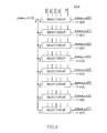
- the semiconductor device 1 includes 16 banks that include respective memory arrays 11 - 0 to 11 - 15 shown in the diagram.
- the memory arrays 11 - 0 to 11 - 15 each include two portions, i.e., one (first memory array) arranged closer to one end (upper in the diagram) of the semiconductor device 1 in a y direction (second direction) and one (second memory array) arranged closer to the other end (lower in the diagram) of the semiconductor device 1 in the y direction.
- the upper and lower portions are arranged in respective rows in a bank order from one end (left in the diagram) to the other end (right in the diagram) of the semiconductor device 1 in an x direction.
- a wiring area AA for arranging various circuits and wiring is provided between the portions of the memory arrays arranged to the bottom in the diagram and those of the memory arrays arranged to the top in the diagram.
- the wiring area AA includes: main amplifiers 13 - 0 to 13 - 15 for the respective memory arrays; a central control circuit 2 including the BOC circuit 17 ( FIG. 4 ); an input circuit 3 including the command decoder 64 ( FIG. 4 ); the eight data input/output terminals 54 corresponding to DQ 0 to DQ 7 , respectively; and the DBI terminal 55 .
- the main amplifiers 13 - 0 to 13 - 15 are main amplifiers corresponding to the memory arrays 11 - 0 to 11 - 15 , respectively.
- the main amplifiers 13 - 0 to 13 - 15 are also divided and arranged to the top and bottom in the diagram so as to correspond to the portions of the memory arrays.
- the main amplifiers 13 - 0 to 13 - 15 are connected to the corresponding memory arrays 11 - 0 to 11 - 15 through 64 main I/O lines MIOT/B (32 upper lines and 32 lower lines in the diagram) each.
- the central control circuit 2 is arranged near the center of the wiring area AA.
- the central control circuit 2 includes the RWBUS control circuit 16 , the BOC circuit 17 , the DBI circuit 18 , and the control circuit 30 shown in FIG. 4 .
- the RWBUS control circuit 16 is connected to the main amplifiers 13 - 0 to 13 - 15 through 64 lines of a read/write bus RWBUS_ARAY.
- the read/write bus RWBUS_ARAY includes 64 lines of a left read/write bus RWBUS_ARAY_le (fifth data lines) and 64 lines of a right read/write bus RWBUS_ARAY_ri (sixth data lines).
- the 64 lines of the left read/write bus RWBUS_ARAY_le include portions extending straight from the central control circuit 2 to one end (left in the diagram) of the semiconductor device 1 in the x direction (first direction), and are connected to the main amplifiers 13 - 0 to 13 - 7 on the way.
- the 64 lines of the right read/write bus RWBUS_ARAY_ri include portions extending straight from the central control circuit 2 to the other one end (right in the diagram) of the semiconductor device 1 in the x direction, and are connected to the main amplifiers 13 - 8 to 13 - 15 on the way.
- the main amplifiers are thus connected with the common read/write bus RWBUS_ARAY. Since the memory arrays 11 other than that selected by the bank address BA are disconnected from the read/write bus RWBUS_ARAY by the control circuit 30 as described above, the number of main amplifiers simultaneously connected to the RWBUS control circuit 16 is one.
- the 64 lines of the left read/write bus RWBUS_ARAY_le each include an intermediate buffer 15 between the portion where the main amplifier 13 - 4 is connected and the portion where the main amplifier 13 - 5 is connected.
- the lines of the right read/write bus RWBUS_ARAY_ri each include an intermediate buffer 15 between the portion where the main amplifier 13 - 11 is connected and the portion where the main amplifier 13 - 12 is connected.
- the intermediate buffers 15 are provided for the purpose of preventing the signals from attenuation during passage through the read/write bus RWBUS_ARAY.
- the input circuit 3 is arranged closer to one end (left in the diagram) of the semiconductor device 1 in the x direction as seen from the central control circuit 2 .
- a group of first pads including a group of address pads connected to the address terminal 53 and a group of command pads connected to the command terminals 52 is arranged near the input circuit 3 in the wiring area AA.
- the input circuit 3 includes the input latch circuit 65 and the latch circuit 66 shown in FIG. 4 . As shown in FIG. 5 , the input circuit 3 functions to supply the bank address BA, the column address Y 0 , Y 1 , and Y 2 , and the like to the central control circuit 2 .
- the eight data input/output terminals 54 and the DBI terminal 55 are arranged closer to the other end (right in the diagram) of the semiconductor device 1 in the x direction as seen from the central control circuit 2 .
- portions of the input/output circuit 19 shown in FIG. 4 corresponding to the data input/output terminals 54 and the DBI terminal 55 are arranged near the respective terminals.
- a group of second pads including groups of DQ pads respectively connected to the data input/output terminals 54 and the DBI terminal 55 is also arranged near the terminals.
- the data input/output terminals 54 are connected to the DBI circuit 18 in the central control circuit 2 through eight lines of the read/write bus RWBUS_DQ each.
- the DBI terminal 55 is connected to the DBI circuit 18 in the central control circuit 2 through the eight lines of the read/write bus RWBUS_DBI.
- the left bank activation signal BA_le, the right bank activation signal BA_ri, the write control clock signal DWCLK, the read control clock signal DRCLK, the write control signal WT, the read control signal RD, and the DBI enable signal DBI_en are signals generated by the control circuit 30 as described above.
- the RWBUS control circuit 16 has an input/output node 16 a which is connected to the 64 lines of the data bus drwbus_in.
- the left bank activation signal BA_le, the right bank activation signal BA_ri, the write control clock signal DWCLK, and the read control clock signal DRCLK are supplied from the control circuit 30 to the RWBUS control circuit 16 .
- the RWBUS control circuit 16 is a circuit (multiplexer) that connects the 64 lines of the data bus drwbus_in with either the 64 lines of the left read/write bus RWBUS_ARAY_le or the 64 lines of the right read/write bus RWBUS_ARAY_ri based on the signals supplied from the control circuit 30 .
- the RWBUS control circuit 16 includes a select circuit 16 b which is arranged between the input/output node 16 a and the left read/write bus RWBUS_ARAY_le, and a select circuit 16 c which is arranged between the input/output node 16 a and the right read/write bus RWBUS_ARAY_ri.
- the select circuit 16 b is provided for each of the 64 lines of the left read/write bus RWBUS_ARAY_le.
- the select circuit 16 c is provided for each of the 64 lines of the right read/write bus RWBUS_ARAY_ri.
- the select circuit 16 b includes inverter circuits 1001 e and 1011 e and NAND circuits 1021 e and 1031 e .
- the select circuit 16 c includes inverter circuits 100 ri and 101 ri and NAND circuits 102 ri and 103 ri.
- the write control clock signal DWCLK is supplied to the NAND circuits 1021 e and 102 ri .
- the read control clock signal DRCLK is supplied to the NAND circuits 1031 e and 103 ri .
- the left bank activation signal BA_le is supplied to the NAND circuits 1021 e and 1031 e .
- the right bank activation signal BA_ri is supplied to the NAND circuits 102 ri and 103 ri .
- the output signals of the NAND circuits 1021 e , 102 ri , 1031 e , and 103 ri are inverted and supplied to the inverter circuits 1001 e , 100 ri , 1011 e , and 101 ri , respectively.
- the output terminal of the inverter circuit 1001 e and the input terminal of the inverter circuit 1011 e are connected in common to the corresponding line of the left read/write bus RWBUS_ARAY_le.
- the input terminal of the inverter circuit 1001 e and the output terminal of the inverter circuit 1011 e are connected in common to the corresponding line of the data bus drwbus_in.
- the output terminal of the inverter circuit 100 ri and the input terminal of the inverter circuit 101 ri are connected in common to the corresponding line of the right read/write bus RWBUS_ARAY_ri.
- the input terminal of the inverter circuit 100 ri and the output terminal of the inverter circuit 101 ri are connected in common to the corresponding line of the data bus drwbus_in.
- either one of the left read/write bus RWBUS_ARAY_le and the right read/write bus RWBUS_ARAY_ri corresponding to the memory array 11 selected by the bank address BA is connected to the data bus drwbus_in through the inverter circuits 1001 e or 100 ri at the time of writing, and through the inverter circuits 1011 e or 101 ri at the time of reading.
- the memory array 11 selected by the bank address BA is thereby connected to the 64 lines of the data bus drwbus_in.
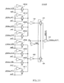
- the BOC circuit 17 includes eight BOC circuits 17 - 0 to 17 - 7 , which are each connected with eight lines of the data bus drwbus_in and eight lines of the data bus drwbus_out. Specifically, the BOC circuit 17 - 0 is connected with the data bus drwbus_in[7:0] and the data bus drwbus_out[7:0]. The BOC circuit 17 - 1 is connected with the data bus drwbus_in[15:8] and the data bus drwbus_out[15:8]. The same holds for the other BOC circuits 17 - 2 to 17 - 7 .
- the central control circuit 2 also includes a bypass circuit that connects the data bus drwbus_in and the data bus drwbus_out through the switch 20 instead of the BOC circuit 17 .
- the column address Y 0 , Y 1 , and Y 2 and the read control signal RD are supplied to the BOC circuits 17 - 0 to 17 - 7 .
- the write control signal WT is supplied to the switch 20 .
- the BOC circuits 17 - 0 to 17 - 7 are configured to operate (perform rearrangement) only when the read control signal RD is activated.
- the switch 20 is configured to operate (pass signals) only when the write control signal WT is activated. As a result, the BOC circuit 17 becomes active only at the time of reading. At the time of writing, the write data is passed through the bypass circuit via the switch 20 , skipping the BOC circuit 17 .
- the BOC circuits 17 - 1 to 17 - 7 have the same configuration as the described BOC circuits 17 - 0 .
- the BOC circuit 17 - 0 includes eight select circuits 17 - 0 [7:0].
- the select circuits 17 - 0 [7:0] are each connected with all the eight lines of the data bus drwbus_in[7:0] and a corresponding line of the data bus drwbus_out [7:0].
- the select circuits 17 - 0 [7:0] each have the function of selecting any one of the eight lines of the data bus drwbus_in[7:0] according to the column address Y 0 , Y 1 , and Y 2 , and connecting the selected line to the corresponding data bus drwbus_out[7:0].
- the select circuit 17 - 0 [0] is supplied with the column address Y 2 and address information Y 00 , Y 01 , Y 10 , and Y 11 .
- the address information Y 00 , Y 01 , Y 10 , and Y 11 is information generated inside the BOC circuit 17 based on the column address Y 0 and Y 1 supplied from the control circuit 30 ( FIG. 4 ).
- the BOC circuit 17 includes NAND circuits 110 to 113 .
- the column address Y 0 and Y 1 is supplied to the NAND circuit 110 .
- the column address Y 0 and the inverted signal of the column address Y 1 are supplied to the NAND circuit 111 .
- the inverted signal of the column address Y 0 and the column address Y 1 are supplied to the NAND circuit 112 .
- the inverted signals of the respective column address Y 0 and Y 1 are supplied to the NAND circuit 113 .
- the pieces of address information Y 00 , Y 01 , Y 10 , and Y 11 become “0” when the combination of the column address Y 0 and Y 1 is (1,1), (1,0), (0,1), and (0,0), respectively, and “1” in the other cases.
- select signals sel 0 to sel 3 are supplied to the select circuit 17 - 0 [0].
- the select signals sel 0 to sel 3 are signals generated by a not-shown circuit in the select circuit 17 - 0 [0].
- the combinations of the values of the select signals sel 0 to sel 3 are determined in advance in association with the combinations of the values of the address information Y 00 , Y 01 , Y 10 , and Y 11 on a one-to-one basis.
- Table 1 shows an example of the associations.
- the select signals sel 0 to sel 3 are (1,1,1,0).
- the select circuits 17 - 0 [7:0] each store associations like Table 1.
- the select circuits 17 - 0 [7:0] read the select signals sel 0 to sel 3 associated with the input address information Y 00 , Y 01 , Y 10 , and Y 11 , and use the select signals sel 0 to sel 3 for the processing to be described below.
- the select circuit 17 - 0 [0] includes transfer gates 120 [7:0], 123 , and 124 , and inverter circuits 121 , 122 , and 125 .
- Each transfer gate includes a P-channel MOS transistor and an N-channel MOS transistor which are connected in parallel.
- the select signal sel 0 and the inverted signal of the select signal sel 0 are supplied to the gates of the P-channel MOS transistor and the N-channel MOS transistor constituting the transfer gate 120 [0], respectively.
- the transfer gate 120 [0] thus becomes conducting if the select signal sel 0 has a logic level of “0”.
- the transfer gate 120 [0] becomes non-conducting if the select signal sel 0 has a logic level of “1”.
- the transfer gates 120 [1] and 120 [5] become conducting if the select signal sell has a logic level of “0”, and become non-conducting if “1”.
- the transfer gates 120 [2] and 120 [6] become conducting if the select signal sell has a logic level of “0”, and become non-conducting if “1”.
- the transfer gates 120 [3] and 120 [7] become conducting if the select signal sel 3 has a logic level of “0”, and become non-conducting if “1”.
- the transfer gate 120 [4] becomes conducting if the select signal sel 0 has a logic level of “0”, and becomes non-conducting if “1”.
- the input terminals of the transfer gates 120 [7:0] are connected to the data bus drwbus_in[7:0], respectively.
- the output terminals of the transfer gates 120 [3:0] are connected in common to the input terminal of the transfer gate 123 through the inverter circuit 121 .
- the output terminals of the transfer gates 120 [7:4] are connected in common to the input terminal of the transfer gate 124 through the inverter circuit 122 .
- the select signals sel 0 to sel 3 are configured so that anyone of the select signals sel 0 to sel 3 becomes “0” while the others are “1”.
- the input terminal of the transfer gate 123 is thus connected with only one of the lines of the data bus drwbus_in[3:0].
- the input terminal of the transfer gate 124 is connected with only one of the lines of the data bus drwbus_in[7:4].
- the column address Y 2 and the inverted signal Y 2 B of the column address Y 2 are supplied to the gates of the P-channel MOS transistor and the N-channel MOS transistor constituting the transfer gate 123 , respectively. Consequently, the transfer gate 123 becomes conducting if the column address Y 2 has a logic level of “0”, and becomes non-conducting if “1”.
- the inverted signal Y 2 B of the column address Y 2 and the column address Y 2 are supplied to the gates of the P-channel MOS transistor and the N-channel MOS transistor constituting the transfer gate 124 , respectively. Consequently, the transfer gate 124 becomes conducting if the column address Y 2 has a logic level of “1”, and becomes non-conducting if “0”.
- the output terminals of the transfer gates 123 and 124 are connected in common to the input terminal of the inverter circuit 125 .
- the inverted signal of the read control clock signal DRCLK is supplied to the inverter circuit 125 .
- the inverter circuit 125 connects the output terminals of the transfer gates 123 and 124 to the data bus drwbus_out[0] at timing corresponding to the read control clock signal DRCLK.
- the address information Y 00 , Y 01 , Y 10 , and Y 11 and the select signals sel 0 to sel 3 are associated as shown in Table 1.
- the data bus drwbus_out[0] is connected with the data bus drwbus_in shown by the following Table 2 depending on the combination of the column address Y 0 , Y 1 , and Y 2 .
- the select circuit 17 - 0 [0] can thus connect any one of the eight lines of the data bus drwbus_in[7:0] to the data bus drwbus_out[0] in accordance with the column address Y 0 , Y 1 , and Y 2 .
- the select circuit 17 - 0 [0] is a circuit that controls the data to be supplied to the data bus drwbus_out[0].
- the other select circuits 17 - 0 [7:1] control the data to be supplied to the data bus drwbusout [7:1], respectively.
- the output order in which the eight bits of read data DQ are burst output from the data input/output terminal 54 [0] can thus be rearranged (BOC) in accordance with the column address Y 0 , Y 1 , and Y 2 by changing the associations of the select signals sel 0 to sel 3 with the address information Y 00 , Y 01 , Y 10 , and Y 11 from one to another of the select circuits 17 - 0 [7:0] so that the pieces of data supplied to the data bus drwbus_out[7:0] do not overlap each other.
- the DBI circuit 18 is connected to the 64 lines of the data bus drwbus_out[63:0], the 64 lines of the read/write bus RWBUS_DQ[63:0], and the eight lines of the read/write bus RWBUS_DBI[7:0]. At the time of reading, the DBI circuit 18 functions to invert the read data DQ input through the data bus drwbus_out in accordance with a predetermined condition and generate DBI data that indicates information on the inversion.
- the DBI circuit 18 performs processing for re-inverting and restoring inverted pieces of write data DQ that is input from outside through the read/write bus RWBUS_DQ, in accordance with DBI data that is input from outside through the read/write bus RWBUS_DBI.
- a read-related configuration will be described below.
- the DBI circuit 18 includes one internal circuit for each order of the burst output.
- FIG. 11 shows only the internal circuit corresponding to the zeroth output order.
- the internal circuits corresponding to the other output orders have the same configuration.
- FIG. 11 only shows the read-related configuration.
- a write-related configuration is omitted.
- the read data corresponding to the zeroth output order includes the eight pieces of read data DQ[8 ⁇ 0+0] to DQ[8 ⁇ 7+0] (read data DQ[0] to DQ[56]).
- the DBI circuit 18 includes a majority circuit 18 d and a majority circuit 18 e .
- the majority circuit 18 d will initially be described.
- the majority circuit 18 d includes NAND circuits 130 , 132 , 134 , 136 , 174 , and 175 , NOR circuits 131 , 133 , 135 , 137 , 141 , 143 , 144 , 145 , 149 , 151 , 152 , 153 , 154 , 155 , 156 , 158 , 159 , and 160 , inverter circuits 138 , 139 , 140 , 142 , 146 , 146 , 148 , 150 , 157 , 161 , and OR circuits 170 , 171 , 172 , 173 , and 176 .
- the connections of such circuits will be described below.
- the data bus drwbus_out[56] and the data bus drwbus_out[48] are connected to and the DBI enable signal DBI_en is supplied to the input terminals of the NAND circuit 130 .
- the data bus drwbus_out[56] and the data bus drwbus_out[48] are connected to and the inverted signal of the DBI enable signal DBI_en is supplied to the input terminals of the NOR circuit 131 .
- the data bus drwbus_out[40] and the data bus drwbus_out[32] are connected to and the DBI enable signal DBI_en is supplied to the input terminals of the NAND circuit 132 .
- the data bus drwbus_out[40] and the data bus drwbus_out[32] are connected to and the inverted signal of the DBI enable signal DBI_en is supplied to the input terminals of the NOR circuit 133 .
- the data bus drwbus_out [24] and the data bus drwbus_out [16] are connected to and the DBI enable signal DBI_en is supplied to the input terminals of the NAND circuit 134 .
- the data bus drwbus_out[24] and the data bus drwbus_out[16] are connected to and the inverted signal of the DBI enable signal DBI_en is supplied to the input terminals of the NOR circuit 135 .
- the data bus drwbus_out [8] and the data bus drwbus_out[0] are connected to and the DBI enable signal DBI_en is supplied to the input terminals of the NAND circuit 136 .
- the data bus drwbus_out[8] and the data bus drwbus_out[0] are connected to and the inverted signal of the DBI enable signal DBI_en is supplied to the input terminals of the NOR circuit 137 .
- the output signal of the NAND circuit 130 is supplied to the inverter circuit 138 and the NOR circuits 141 and 143 .
- the output signal of the NOR circuit 131 is supplied to the inverter circuit 140 and the NOR circuits 144 and 145 .
- the output signal of the NAND circuit 132 is supplied to the inverter circuit 139 and the NOR circuits 141 and 144 .
- the output signal of the NOR circuit 133 is supplied to the inverter circuit 142 and the NOR circuits 143 and 145 .
- the output signal of the NAND circuit 134 is supplied to the inverter circuit 146 and the NOR circuits 149 and 151 .
- the output signal of the NOR circuit 135 is supplied to the inverter circuit 148 and the NOR circuits 152 and 153 .
- the output signal of the NAND circuit 136 is supplied to the inverter circuit 147 and the NOR circuits 149 and 152 .
- the output signal of the NOR circuit 137 is supplied to the inverter circuit 150 and the NOR circuits 151 and 153 .
- the output signals of the inverter circuits 138 and 139 are supplied to the input terminals of the NOR circuit 154 .
- the output signals of the inverter circuits 140 and 142 and the NOR circuit 141 are supplied to the input terminals of the NOR circuit 155 .
- the output signals of the NOR circuits 143 and 144 are supplied to the input terminals of the NOR circuit 156 .
- the output signal of the NOR circuit 145 is supplied to the input terminal of the inverter circuit 157 .
- the output signals of the inverter circuits 146 and 147 are supplied to the input terminals of the NOR circuit 158 .
- the output signals of the inverter circuits 148 and 150 and the NOR circuit 149 are supplied to the input terminals of the NOR circuit 159 .
- the output signals of the NOR circuits 151 and 152 are supplied to the input terminals of the NOR circuit 160 .
- the output signal of the NOR circuit 153 is supplied to the input terminal of the in
- the output signals of the NOR circuit 154 and the inverter circuit 161 are supplied to the input terminals of the OR circuit 170 .
- the output signals of the NOR circuits 155 and 160 are supplied to the input terminals of the OR circuit 171 .
- the output signals of the inverter circuit 157 and the NOR circuit 158 are supplied to the input terminals of the OR circuit 172 .
- the output signals of the NOR circuits 156 and 159 are supplied to the input terminals of the OR circuit 173 .
- the output signals of the OR circuits 170 and 171 are supplied to the input terminals of the NAND circuit 174 .
- the output signals of the OR circuits 172 and 173 are supplied to the input terminals of the NAND circuit 175 .
- the output signals of the NAND circuits 174 and 175 are supplied to the input terminal of the OR circuit 176 .
- the output signal of the OR circuit 176 constitutes the DBI data DBI[0] corresponding to the zeroth output order.
- the logic level of the DBI data DBI[0] always becomes “0” if the number of pieces of read data DQ that have a logic level of “0” among the eight pieces of read data DQ[8 ⁇ 0+0] to DQ[8 ⁇ 7+0] corresponding to the zeroth output order is greater than or equal to five (more than half).
- the logic level of the DBI data DBI[0] always becomes “1” if the number is smaller than or equal to three (less than half). If the number of pieces of read data DQ having a logic level of “0” is four (the exact half), the logic level of the DBI data DBI[0] may become “0” or “1”. This, however, does not matter because inverting the read data by DBI causes no change in the number of 0s.
- the majority circuit 18 e includes XNOR circuits 180 to 187 and inverter circuits 188 and 190 to 198 .
- the data bus drwbus_out [8 ⁇ 7] to drwbus_out [8 ⁇ 0] and the DBI data DBI[0] are supplied to the input terminals of the XNOR circuits 180 to 187 .
- the DBI data DBI[0] is also supplied to the input terminal of the inverter circuit 188 .
- the output signals of the XNOR circuits 180 to 187 and the inverter circuit 188 are supplied to the inverter circuits 190 to 198 , respectively.
- the output terminals of the inverter circuits 190 to 198 are supplied to the read/write bus RWBUS_DQ[8 ⁇ 7] to RWBUS_DQ[8 ⁇ 0] and the read/write bus RWBUS_DBI[0], respectively.
- the inverter circuits 190 to 198 are supplied with the inverted signal of the read control clock signal DRCLK (not shown). When the read control clock signal DRCLK is activated, the inverter circuits 190 to 198 output the inverted signals of the corresponding XNOR circuits and the inverter circuit to the respective corresponding lines of the read/write bus RWBUS_DQ.
- the majority circuit 18 e simply supplies the data on the data bus drwbus_out[8 ⁇ 0+0] to drwbus_out[8 ⁇ 7+0] to the read/write bus RWBUS_DQ[8 ⁇ 0] to RWBUS_DQ[8 ⁇ 7], respectively, if the DBI data DBI [0] is “1.” On the other hand, if the DBI data DBI[0] is “0,” the majority circuit 18 e inverts the data on the data bus drwbus_out[8 ⁇ 0+0] to drwbus_out[8 ⁇ 7+0] and outputs the resultant to the read/write bus RWBUS_DQ[8.0] to RWBUS_DQ[8 ⁇ 7], respectively. As a result, when five or more of the eight bits (DQ 0 to DQ 7 ) of read data to be simultaneously output are “0”, all the eight bits are inverted (DBI).
- FIG. 12 shows an example where two read commands READ are supplied from outside to the semiconductor device 1 in succession. The following description will be given also with reference to FIG. 4 .
- the read data DQ[63:0] is supplied to the data bus drwbus_in[63:0] through the RWBUS control circuit 16 .
- the BOC circuit 17 rearranges the output order of the pieces of read data for each data input/output terminal 54 , and outputs the resultant to the data bus drwbus_out[63:0].
- the DBI circuit 18 then converts the read data DQ[63:0] so that five or more of eight bits (DQ 0 to DQ 7 ) of the read data to be simultaneously output are “1,” and outputs the resultant to the read write bus RWBUS_DQ[63:0].
- the DBI circuit 18 simultaneously generates DBI data DBI[7:0] indicating whether the read data is inverted, and outputs the DBI data DBI[7:0] to the read/write bus RWBUS_DBI[7:0].
- the read data DQ[63:0] and the DBI data DBI[7:0] thus output to the respective read/write buses are supplied to the input/output circuit 19 .
- the read data DQ[63:0] and the DBI data DBI[7:0] are burst output from the corresponding data input/output terminals 54 and DBI terminal 55 in units of eight bits in synchronization with the external clock CK after a predetermined read latency (“7” in the example of FIG. 12 ).
- the provision of the DBI circuit 18 between the BOC circuit 17 and the input/output circuit 19 eliminates the need for a BOC circuit 17 that is intended to rearrange the order of the DBI data.
- FIG. 13 corresponds to FIG. 6 which shows the semiconductor device 1 according to the present embodiment.
- the semiconductor device 200 includes a DBI circuit 202 between a BOC circuit 203 and an RWBUS control circuit 201 .
- a data bus drwbus_dbi needs to be arranged between the DBI circuit 202 and the BOC circuit 202
- the BOC circuit 202 needs to include a ninth BOC circuit 202 - 8 .
- the DBI circuit 202 generates eight bits of DBI data corresponding to respective orders of output (n) from the 64 bits of data on the data bus drwbus_in[63:0]. Since the DBI data also needs to be rearranged by the BOC circuit 203 , the BOC circuit 203 needs to include the ninth BOC circuit 203 - 8 .
- the semiconductor device 1 according to the present embodiment does not need such components.
- the presence of the data bus drwbus_dbi and the BOC circuit 203 - 8 increases the circuit area and power consumption of the semiconductor device 200 as compared to the semiconductor device 1 .
- the semiconductor device 1 according to the present embodiment thus has a reduced circuit area and power consumption as compared to the semiconductor device 200 according to the comparative example.
- the data processing system 800 includes a structure in which the following components are connected to each other via a system bus 810 : a data processor 820 (controller); a DRAM 1 , which is the semiconductor device 1 of the present embodiment; a storage device 840 ; an I/O device 850 ; and a ROM 860 .
- the data processor 820 includes a function of supplying external clock signals CK and /CK to the DRAM 10 , and a function of receiving an output signal (read data DQ) of the input/output circuit 19 ( FIG. 4 ) of the DRAM 1 and performing a process corresponding to the received read data DQ. More specifically, for example, the following can be used as the data processor 820 : a microprocessor (MPU), a digital signal processor (DSP), and the like. Incidentally, the data processor 820 and the DRAM 1 may be connected to each other by a local bus, not via the system bus 810 .
- MPU microprocessor
- DSP digital signal processor
- the storage device 840 a hard disk drive, an optical disc drive, a flash memory, or the like may be used.
- a display device such as a liquid crystal display, an input device such as a keyboard and mouse, or the like may be used.
- the I/O device 850 may be either an input device or an output device.
- FIG. 14 shows only one system bus 810 for ease of explanation. However, a plurality of system buses 810 may be provided in a serial or parallel manner via a connector or the like, if necessary.
- the storage device 840 , the I/O device 850 , and the ROM 860 are not necessarily essential components. Furthermore, in FIG. 14 , for ease of explanation, there is only one depicted per each type of component. However, the present invention is not limited to the above case. As for one, two, or more types of component, there may be provided more than one per type.
- the memory cells according to the present invention may be volatile, nonvolatile, or a combination of these.
- the technical concept of the present invention may be applied to a semiconductor device that includes a signal transmission circuit.
- the forms of the circuits in the circuit blocks disclosed in the drawings and other circuits for generating the control signals are not limited to the circuit forms disclosed in the embodiment.
- the present invention can be applied to various types of semiconductor devices.
- the present invention can be applied to a general semiconductor device such as a CPU (Central Processing Unit), an MCU (Micro Control Unit), a DSP (Digital Signal Processor), an ASIC (Application Specific Integrated Circuit), an ASSP (Application Specific Standard Circuit), and a Memory.
- An SOC System on Chip
- An MCP Multi Chip Package
- a POP Package on Package
- the present invention can be applied to the semiconductor device that has these arbitrary product form and package form.
- transistors When the transistors are field effect transistors (FETs), various FETs are applicable, including MIS (Metal Insulator Semiconductor) and TFT (Thin Film Transistor) as well as MOS (Metal Oxide Semiconductor).
- MIS Metal Insulator Semiconductor
- TFT Thin Film Transistor
- MOS Metal Oxide Semiconductor
- the device may even include bipolar transistors.
- NMOS transistor N-channel MOS transistor
- PMOS transistor P-channel MOS transistor
- a data processing system includes: a semiconductor device including a plurality of first data lines that transmit a plurality of sequential first data bits, respectively, a plurality of second data lines that transmit a plurality of sequential second data bits, respectively, a plurality of third data lines that transmit a plurality of sequential third data bits, respectively, a BOC circuit that rearranges order of the plurality of first data bits supplied from the plurality of first data lines in accordance with address information, and supplies the resultant to the plurality of second data lines as the plurality of second data bits, and a DBI circuit that performs inversion or non-inversion of the plurality of second data bits supplied from the plurality of second data lines independently of each other in accordance with a predetermined condition, and supplies the resultant to the plurality of third data lines as the plurality of third data bits; and a controller that controls the semiconductor device.
- the data processing system may be configured such that: the semiconductor device includes a mode register that stores an operation mode signal indicating an operation mode; the DBI circuit performs inversion processing in accordance with the operation mode indicated by the operation mode signal; and the controller sets the operation mode signal into the mode register.
Landscapes
- Engineering & Computer Science (AREA)
- Theoretical Computer Science (AREA)
- Databases & Information Systems (AREA)
- Microelectronics & Electronic Packaging (AREA)
- Computer Hardware Design (AREA)
- Physics & Mathematics (AREA)
- General Engineering & Computer Science (AREA)
- General Physics & Mathematics (AREA)
- Dram (AREA)
- Dc Digital Transmission (AREA)
Abstract
Description
| TABLE 1 | |||||||
| Y00 | Y01 | Y10 | Y11 | se10 | se11 | se12 | se13 |
| 0 | 1 | 1 | 1 | 1 | 1 | 1 | 0 |
| 1 | 0 | 1 | 1 | 1 | 1 | 0 | 1 |
| 1 | 1 | 0 | 1 | 1 | 0 | 1 | 1 |
| 1 | 1 | 1 | 0 | 0 | 1 | 1 | 1 |
| 0 | 1 | 1 | 1 | 1 | 1 | 1 | 0 |
| 1 | 0 | 1 | 1 | 1 | 1 | 0 | 1 |
| 1 | 1 | 0 | 1 | 1 | 0 | 1 | 1 |
| 1 | 1 | 1 | 0 | 0 | 1 | 1 | 1 |
| TABLE 2 | |||||
| data bus connecting to | |||||
| Y2 | Y1 | Y0 | data bus drwbus_out[0] | ||
| 1 | 1 | 1 | drwbus_in[7] | ||
| 1 | 1 | 0 | drwbus_in[6] | ||
| 1 | 0 | 1 | drwbus_in[5] | ||
| 1 | 0 | 0 | drwbus_in[4] | ||
| 0 | 1 | 1 | drwbus_in[3] | ||
| 0 | 1 | 0 | drwbus_in[2] | ||
| 0 | 0 | 1 | drwbus_in[1] | ||
| 0 | 0 | 0 | drwbus_in[0] | ||
Claims (20)
Applications Claiming Priority (2)
| Application Number | Priority Date | Filing Date | Title |
|---|---|---|---|
| JP2011-214450 | 2011-09-29 | ||
| JP2011214450A JP5972549B2 (en) | 2011-09-29 | 2011-09-29 | Semiconductor device |
Publications (2)
| Publication Number | Publication Date |
|---|---|
| US20130091327A1 US20130091327A1 (en) | 2013-04-11 |
| US8862811B2 true US8862811B2 (en) | 2014-10-14 |
Family
ID=47262995
Family Applications (1)
| Application Number | Title | Priority Date | Filing Date |
|---|---|---|---|
| US13/629,328 Active 2033-04-16 US8862811B2 (en) | 2011-09-29 | 2012-09-27 | Semiconductor device performing burst order control and data bus inversion |
Country Status (4)
| Country | Link |
|---|---|
| US (1) | US8862811B2 (en) |
| EP (1) | EP2575134B8 (en) |
| JP (1) | JP5972549B2 (en) |
| ES (1) | ES2487819T3 (en) |
Cited By (4)
| Publication number | Priority date | Publication date | Assignee | Title |
|---|---|---|---|---|
| US20160224480A1 (en) * | 2015-01-29 | 2016-08-04 | SK Hynix Inc. | Semiconductor memory apparatus and data input/output method thereof |
| US10031868B2 (en) | 2014-12-09 | 2018-07-24 | Intel Corporation | Dynamic bus inversion with programmable termination level to maintain programmable target ratio of ones and zeros in signal lines |
| US10747695B2 (en) | 2017-10-27 | 2020-08-18 | Samsung Electronics Co., Ltd. | Methods of performing multiple data bus inversion (DBI) and memory devices performing the methods |
| US11467762B2 (en) * | 2019-09-13 | 2022-10-11 | Kioxia Corporation | Data bus inversion (DBI) in a memory system, controller and data transfer method |
Families Citing this family (10)
| Publication number | Priority date | Publication date | Assignee | Title |
|---|---|---|---|---|
| KR102104578B1 (en) * | 2013-08-30 | 2020-04-27 | 에스케이하이닉스 주식회사 | SEMICONDUCTOR APPARATUS WITH Data Bit Inversion |
| KR20150099928A (en) | 2014-02-24 | 2015-09-02 | 삼성전자주식회사 | Semiconductor memory device and memory system including the same |
| US9405721B2 (en) * | 2014-06-06 | 2016-08-02 | Micron Technology, Inc. | Apparatuses and methods for performing a databus inversion operation |
| KR20160117087A (en) | 2015-03-31 | 2016-10-10 | 에스케이하이닉스 주식회사 | Semiconductor device |
| US9922686B2 (en) | 2016-05-19 | 2018-03-20 | Micron Technology, Inc. | Apparatuses and methods for performing intra-module databus inversion operations |
| US10146719B2 (en) | 2017-03-24 | 2018-12-04 | Micron Technology, Inc. | Semiconductor layered device with data bus |
| US10964702B2 (en) | 2018-10-17 | 2021-03-30 | Micron Technology, Inc. | Semiconductor device with first-in-first-out circuit |
| US10838732B2 (en) | 2018-12-21 | 2020-11-17 | Micron Technology, Inc. | Apparatuses and methods for ordering bits in a memory device |
| CN109582507B (en) | 2018-12-29 | 2023-12-26 | 西安紫光国芯半导体股份有限公司 | Data backup and recovery method for NVDIMM, NVDIMM controller and NVDIMM |
| US12183386B2 (en) * | 2022-09-06 | 2024-12-31 | SanDisk Technologies, Inc. | Optimization of non-aligned host writes |
Citations (8)
| Publication number | Priority date | Publication date | Assignee | Title |
|---|---|---|---|---|
| JPH06290582A (en) | 1993-04-02 | 1994-10-18 | Nec Corp | Semiconductor memory |
| US5890005A (en) * | 1997-06-02 | 1999-03-30 | Nokia Mobile Phones Limited | Low power, low interconnect complexity microprocessor and memory interface |
| US20060261929A1 (en) * | 2005-03-22 | 2006-11-23 | Thomas Hein | Circuit for producing a data bit inversion flag |
| US7405981B2 (en) | 2005-03-11 | 2008-07-29 | Infineon Technologies Ag | Circuit for data bit inversion |
| US20100077125A1 (en) * | 2008-09-22 | 2010-03-25 | Hynix Semiconductor Inc. | Semiconductor memory device |
| US20100118618A1 (en) * | 2008-11-13 | 2010-05-13 | Seung Wook Kwak | Semiconductor integrated circuit with data bus inversion function |
| WO2013007048A1 (en) * | 2011-07-11 | 2013-01-17 | 澜起科技(上海)有限公司 | Data read/write system |
| US20130061102A1 (en) * | 2011-09-06 | 2013-03-07 | Samsung Electronics Co., Ltd. | Semiconductor memory device |
Family Cites Families (4)
| Publication number | Priority date | Publication date | Assignee | Title |
|---|---|---|---|---|
| US6463003B2 (en) * | 2000-06-07 | 2002-10-08 | Advanced Micro Devices, Inc. | Power saving scheme for burst mode implementation during reading of data from a memory device |
| KR100546339B1 (en) * | 2003-07-04 | 2006-01-26 | 삼성전자주식회사 | Semiconductor device capable of selectively implementing a single data strobe mode with a differential data strobe mode and a data inversion scheme |
| US7133324B2 (en) * | 2003-12-24 | 2006-11-07 | Samsung Electronics Co., Ltd. | Synchronous dynamic random access memory devices having dual data rate 1 (DDR1) and DDR2 modes of operation and methods of operating same |
| KR100800160B1 (en) * | 2006-09-07 | 2008-02-01 | 주식회사 하이닉스반도체 | Data output circuit of semiconductor memory device |
-
2011
- 2011-09-29 JP JP2011214450A patent/JP5972549B2/en active Active
-
2012
- 2012-09-27 EP EP12186309.6A patent/EP2575134B8/en not_active Not-in-force
- 2012-09-27 ES ES12186309.6T patent/ES2487819T3/en active Active
- 2012-09-27 US US13/629,328 patent/US8862811B2/en active Active
Patent Citations (11)
| Publication number | Priority date | Publication date | Assignee | Title |
|---|---|---|---|---|
| JPH06290582A (en) | 1993-04-02 | 1994-10-18 | Nec Corp | Semiconductor memory |
| US5426606A (en) | 1993-04-02 | 1995-06-20 | Nec Corporation | Semiconductor memory device synchronous with external clock signal for outputting data bits through a small number of data lines |
| USRE35934E (en) | 1993-04-02 | 1998-10-27 | Nec Corporation | Semiconductor memory device synchronous with external clock signal for outputting data bits through a small number of data lines |
| US5890005A (en) * | 1997-06-02 | 1999-03-30 | Nokia Mobile Phones Limited | Low power, low interconnect complexity microprocessor and memory interface |
| US7405981B2 (en) | 2005-03-11 | 2008-07-29 | Infineon Technologies Ag | Circuit for data bit inversion |
| US20060261929A1 (en) * | 2005-03-22 | 2006-11-23 | Thomas Hein | Circuit for producing a data bit inversion flag |
| US20100077125A1 (en) * | 2008-09-22 | 2010-03-25 | Hynix Semiconductor Inc. | Semiconductor memory device |
| US20100118618A1 (en) * | 2008-11-13 | 2010-05-13 | Seung Wook Kwak | Semiconductor integrated circuit with data bus inversion function |
| WO2013007048A1 (en) * | 2011-07-11 | 2013-01-17 | 澜起科技(上海)有限公司 | Data read/write system |
| US20130132660A1 (en) * | 2011-07-11 | 2013-05-23 | Montage Technology (Shanghai) Co., Ltd. | Data read/write system |
| US20130061102A1 (en) * | 2011-09-06 | 2013-03-07 | Samsung Electronics Co., Ltd. | Semiconductor memory device |
Cited By (8)
| Publication number | Priority date | Publication date | Assignee | Title |
|---|---|---|---|---|
| US10031868B2 (en) | 2014-12-09 | 2018-07-24 | Intel Corporation | Dynamic bus inversion with programmable termination level to maintain programmable target ratio of ones and zeros in signal lines |
| US10437746B2 (en) | 2014-12-09 | 2019-10-08 | Intel Corporation | Dynamic bus inversion with programmable termination level to maintain programmable target ratio of ones and zeros in signal lines |
| US10802996B2 (en) | 2014-12-09 | 2020-10-13 | Intel Corporation | Dynamic bus inversion with programmable termination level to maintain programmable target ratio of ones and zeros in signal lines |
| US20160224480A1 (en) * | 2015-01-29 | 2016-08-04 | SK Hynix Inc. | Semiconductor memory apparatus and data input/output method thereof |
| US10037291B2 (en) * | 2015-01-29 | 2018-07-31 | SK Hynix Inc. | Semiconductor memory apparatus and data input/output method thereof |
| US10409741B2 (en) | 2015-01-29 | 2019-09-10 | SK Hynix Inc. | Semiconductor memory apparatus and data input/output method thereof |
| US10747695B2 (en) | 2017-10-27 | 2020-08-18 | Samsung Electronics Co., Ltd. | Methods of performing multiple data bus inversion (DBI) and memory devices performing the methods |
| US11467762B2 (en) * | 2019-09-13 | 2022-10-11 | Kioxia Corporation | Data bus inversion (DBI) in a memory system, controller and data transfer method |
Also Published As
| Publication number | Publication date |
|---|---|
| EP2575134A3 (en) | 2013-07-03 |
| EP2575134A2 (en) | 2013-04-03 |
| JP5972549B2 (en) | 2016-08-17 |
| EP2575134B1 (en) | 2014-06-18 |
| US20130091327A1 (en) | 2013-04-11 |
| EP2575134B8 (en) | 2014-08-13 |
| JP2013073665A (en) | 2013-04-22 |
| ES2487819T3 (en) | 2014-08-25 |
Similar Documents
| Publication | Publication Date | Title |
|---|---|---|
| US8862811B2 (en) | Semiconductor device performing burst order control and data bus inversion | |
| US9640233B2 (en) | Semiconductor memory device having inverting circuit and controlling method there of | |
| US20250085847A1 (en) | Apparatuses and methods for configurable memory array bank architectures | |
| US8509020B2 (en) | Data processing system | |
| US10957380B2 (en) | Memory device scrambling address | |
| US20110026290A1 (en) | Semiconductor device having memory cell array divided into plural memory mats | |
| US8467217B2 (en) | Semiconductor device | |
| US8630129B2 (en) | Semiconductor device having plural banks | |
| US10068637B2 (en) | Semiconductor device having PDA function | |
| US20090273991A1 (en) | Semiconductor memory device, operating method thereof, and compression test method thereof | |
| US11494319B1 (en) | Apparatuses, systems, and methods for input/output mappings | |
| US11545211B2 (en) | Semiconductor memory device and a method of operating the semiconductor memory device | |
| US10354717B1 (en) | Reduced shifter memory system | |
| US20100244905A1 (en) | Input buffer circuit of semiconductor device having function of adjusting input level | |
| US7434018B2 (en) | Memory system | |
| US20260065973A1 (en) | Multiplexing for memory packages with buffer die and modules with same | |
| US9396773B2 (en) | Semiconductor device | |
| US9336856B2 (en) | Device and apparatus having address and command input paths | |
| US20250278276A1 (en) | Apparatuses, systems, and methods for mode register page access modes | |
| TW202522476A (en) | Memory device, system, and decoding circuit | |
| KR20010002499A (en) | Data input/output controller for multi bank |
Legal Events
| Date | Code | Title | Description |
|---|---|---|---|
| AS | Assignment |
Owner name: ELPIDA MEMORY INC., JAPAN Free format text: SECURITY AGREEMENT;ASSIGNOR:PS4 LUXCO S.A.R.L.;REEL/FRAME:032414/0261 Effective date: 20130726 |
|
| AS | Assignment |
Owner name: PS4 LUXCO S.A.R.L., LUXEMBOURG Free format text: ASSIGNMENT OF ASSIGNORS INTEREST;ASSIGNOR:ELPIDA MEMORY, INC.;REEL/FRAME:032899/0196 Effective date: 20130726 |
|
| AS | Assignment |
Owner name: ELPIDA MEMORY INC., JAPAN Free format text: ASSIGNMENT OF ASSIGNORS INTEREST;ASSIGNORS:SHIDO, TAIHEI;DONO, CHIAKI;MIYAZAKI, SHINYA;AND OTHERS;SIGNING DATES FROM 20121015 TO 20121025;REEL/FRAME:033529/0477 |
|
| STCF | Information on status: patent grant |
Free format text: PATENTED CASE |
|
| FEPP | Fee payment procedure |
Free format text: PAYOR NUMBER ASSIGNED (ORIGINAL EVENT CODE: ASPN); ENTITY STATUS OF PATENT OWNER: LARGE ENTITY |
|
| AS | Assignment |
Owner name: PS5 LUXCO S.A.R.L., LUXEMBOURG Free format text: ASSIGNMENT OF ASSIGNORS INTEREST;ASSIGNOR:PS4 LUXCO S.A.R.L.;REEL/FRAME:039818/0506 Effective date: 20130829 Owner name: LONGITUDE SEMICONDUCTOR S.A.R.L., LUXEMBOURG Free format text: CHANGE OF NAME;ASSIGNOR:PS5 LUXCO S.A.R.L.;REEL/FRAME:039793/0880 Effective date: 20131112 |
|
| MAFP | Maintenance fee payment |
Free format text: PAYMENT OF MAINTENANCE FEE, 4TH YEAR, LARGE ENTITY (ORIGINAL EVENT CODE: M1551) Year of fee payment: 4 |
|
| AS | Assignment |
Owner name: LONGITUDE LICENSING LIMITED, IRELAND Free format text: ASSIGNMENT OF ASSIGNORS INTEREST;ASSIGNOR:LONGITUDE SEMICONDUCTOR S.A.R.L.;REEL/FRAME:046863/0001 Effective date: 20180731 |
|
| MAFP | Maintenance fee payment |
Free format text: PAYMENT OF MAINTENANCE FEE, 8TH YEAR, LARGE ENTITY (ORIGINAL EVENT CODE: M1552); ENTITY STATUS OF PATENT OWNER: LARGE ENTITY Year of fee payment: 8 |