JP4234082B2 - Power converter - Google Patents
Power converter Download PDFInfo
- Publication number
- JP4234082B2 JP4234082B2 JP2004255286A JP2004255286A JP4234082B2 JP 4234082 B2 JP4234082 B2 JP 4234082B2 JP 2004255286 A JP2004255286 A JP 2004255286A JP 2004255286 A JP2004255286 A JP 2004255286A JP 4234082 B2 JP4234082 B2 JP 4234082B2
- Authority
- JP
- Japan
- Prior art keywords
- gradation
- output
- current
- gradation correction
- correction value
- Prior art date
- Legal status (The legal status is an assumption and is not a legal conclusion. Google has not performed a legal analysis and makes no representation as to the accuracy of the status listed.)
- Active
Links
- 238000006243 chemical reaction Methods 0.000 claims description 22
- 230000007423 decrease Effects 0.000 description 12
- 238000005070 sampling Methods 0.000 description 7
- 238000010586 diagram Methods 0.000 description 6
- 230000007704 transition Effects 0.000 description 4
- 230000003247 decreasing effect Effects 0.000 description 3
- 239000003990 capacitor Substances 0.000 description 2
- 230000003111 delayed effect Effects 0.000 description 2
- 239000000284 extract Substances 0.000 description 2
- 239000004065 semiconductor Substances 0.000 description 2
- 230000005540 biological transmission Effects 0.000 description 1
- 230000000694 effects Effects 0.000 description 1
- 238000000034 method Methods 0.000 description 1
- 238000013508 migration Methods 0.000 description 1
- 230000005012 migration Effects 0.000 description 1
- 230000001629 suppression Effects 0.000 description 1
- 230000001360 synchronised effect Effects 0.000 description 1
Images


Classifications
-
- Y—GENERAL TAGGING OF NEW TECHNOLOGICAL DEVELOPMENTS; GENERAL TAGGING OF CROSS-SECTIONAL TECHNOLOGIES SPANNING OVER SEVERAL SECTIONS OF THE IPC; TECHNICAL SUBJECTS COVERED BY FORMER USPC CROSS-REFERENCE ART COLLECTIONS [XRACs] AND DIGESTS
- Y02—TECHNOLOGIES OR APPLICATIONS FOR MITIGATION OR ADAPTATION AGAINST CLIMATE CHANGE
- Y02E—REDUCTION OF GREENHOUSE GAS [GHG] EMISSIONS, RELATED TO ENERGY GENERATION, TRANSMISSION OR DISTRIBUTION
- Y02E40/00—Technologies for an efficient electrical power generation, transmission or distribution
- Y02E40/40—Arrangements for reducing harmonics
Landscapes
- Supply And Distribution Of Alternating Current (AREA)
Description
この発明は、高調波を発生する負荷機器に対して高調波補償電流を発生し、電源側へ流出する高調波電流を抑制するアクティブフィルタ等に用いる電力変換装置に関するものである。 The present invention relates to a power conversion device used for an active filter or the like that generates a harmonic compensation current for a load device that generates a harmonic and suppresses a harmonic current flowing out to a power supply side.
アクティブフィルタは、高調波電流を発生している負荷機器の直近で高調波電流を相殺する高周波補償電流を発生するものである。従来のアクティブフィルタは、負荷電流を検出して、この負荷電流を基本波電流と高調波電流に分離し、高調波電流のみを取り出してこれと180度位相の異なる高調波補償電流を発生させる。そして、この高調波補償電流を負荷の接続点に注入することにより、負荷電流の高調波電流は相殺され、電源電流は高調波を含まない正弦波となる。このようなアクティブフィルタは、電力用の電流発生源として低損失である高周波PWMインバータが用いられていた(例えば、非特許文献1参照)。 The active filter generates a high-frequency compensation current that cancels out the harmonic current in the immediate vicinity of the load device that generates the harmonic current. A conventional active filter detects a load current, separates the load current into a fundamental wave current and a harmonic current, extracts only the harmonic current, and generates a harmonic compensation current that is 180 degrees out of phase with the harmonic current. Then, by injecting this harmonic compensation current into the connection point of the load, the harmonic current of the load current is canceled out, and the power supply current becomes a sine wave that does not include harmonics. In such an active filter, a high-frequency PWM inverter with low loss is used as a current source for electric power (see, for example, Non-Patent Document 1).
従来のアクティブフィルタは、以上のように高周波PWMインバータが用いられており、このため電源側へ流出する高調波電流を抑制するために大きなフィルタ回路を必要とし、アクティブフィルタの装置構成の小型化が困難であった。 As described above, the conventional active filter uses the high-frequency PWM inverter. Therefore, a large filter circuit is required to suppress the harmonic current flowing out to the power supply side, and the device configuration of the active filter is reduced in size. It was difficult.
この発明は、上記のような問題点を解消するために成されたものであって、出力側のフィルタ回路が格段と低減され小型化の促進された電力変換装置を得ることを目的とする。 The present invention has been made to solve the above-described problems, and an object of the present invention is to obtain a power conversion device in which the output-side filter circuit is remarkably reduced and the miniaturization is promoted.
この発明に係る第1の電力変換装置は、直流電源からの直流電力を交流に変換する単相インバータの交流側を複数直列接続して成る単相インバータ群と、上記複数の単相インバータの中から選択された所定の組み合わせによる各発生電圧の総和により上記単相インバータ群の出力電圧を階調制御し、設定された出力電流を出力させる制御装置とを備える。上記制御装置は、与えられた基準電圧に基づいて上記出力電圧の基本階調を演算する基本階調演算部と、上記出力電流が設定された目標電流に追従するように上記基本階調を補正するための階調補正値を演算する階調補正演算部と、上記基本階調を上記階調補正値にて補正して上記単相インバータ群の出力電圧階調を演算する出力階調演算部と、上記出力電圧階調に基づいて上記単相インバータ群への制御信号を出力するインバータ制御演算部とを備える。そして、上記階調補正演算部は、上記出力電流に複数の閾値を設け、各閾値を越える毎に上記階調補正値を変化させて上記出力電圧階調を変化させるものである。
またこの発明に係る第2の電力変換装置は、交流電源に並列に接続され、直流電源からの直流電力を交流に変換する単相インバータの交流側を複数直列接続して成る単相インバータ群と、上記複数の単相インバータの中から選択された所定の組み合わせによる各発生電圧の総和により上記単相インバータ群の出力電圧を階調制御し、上記交流電源からの電源電流を補正する出力電流を出力させる制御装置とを備える。上記制御装置は、上記交流電源の電源電圧に基づいて上記出力電圧の基本階調を演算する基本階調演算部と、上記出力電流が目標電流に追従するように上記基本階調を補正するための階調補正値を演算する階調補正演算部と、上記基本階調を上記階調補正値にて補正して上記単相インバータ群の出力電圧階調を演算する出力階調演算部と、上記出力電圧階調に基づいて上記単相インバータ群への制御信号を出力するインバータ制御演算部とを備える。そして、上記階調補正演算部は、上記出力電流に複数の閾値を設け、各閾値を越える毎に上記階調補正値を変化させて上記出力電圧階調を変化させるものである。
A first power conversion device according to the present invention includes a single-phase inverter group formed by connecting a plurality of AC sides of a single-phase inverter that converts DC power from a DC power source into AC, and a plurality of single-phase inverters. the output voltage of the single-phase inverter group gradation controlled by the sum of generated voltages from a predetermined combination selected from Ru and a control device which Ru is an output current set. The control device corrects the basic gradation so that the basic gradation calculation unit for calculating the basic gradation of the output voltage based on a given reference voltage and the output current follows a set target current. And a gradation correction calculation unit for calculating a gradation correction value for calculating the output voltage gradation of the single-phase inverter group by correcting the basic gradation with the gradation correction value. And an inverter control arithmetic unit that outputs a control signal to the single-phase inverter group based on the output voltage gradation. The gradation correction calculation unit is configured to provide a plurality of threshold values for the output current, and to change the output voltage gradation by changing the gradation correction value every time each threshold value is exceeded.
A second power conversion device according to the present invention includes a single-phase inverter group that is connected in parallel to an AC power source, and is formed by connecting a plurality of AC sides of a single-phase inverter that converts DC power from a DC power source into AC. The output voltage of the single-phase inverter group is gradation controlled by the sum of the generated voltages by a predetermined combination selected from the plurality of single-phase inverters, and the output current for correcting the power supply current from the AC power supply is adjusted. and a Ru controller is output. Upper Symbol controller corrects the basic tone calculation unit for calculating a basic tone of the output voltage based on the power supply voltage of the AC power supply, the basic tone as the output current follows the target current A gradation correction calculation unit for calculating a gradation correction value for calculating the output voltage gradation of the single-phase inverter group by correcting the basic gradation with the gradation correction value; And an inverter control operation unit that outputs a control signal to the single-phase inverter group based on the output voltage gradation. The gradation correction calculation unit is configured to provide a plurality of threshold values for the output current, and to change the output voltage gradation by changing the gradation correction value every time each threshold value is exceeded.
この発明に係る第1、第2の電力変換装置は、各単相インバータの発生電圧を組み合わせた出力電圧の階調制御を行うため、大きなフィルタ回路を必要とすることなく電源側へ流出する高調波電流を抑制することができ、電力変換装置の装置構成の小型化、簡略化が促進できる。 Since the first and second power conversion devices according to the present invention perform gradation control of the output voltage that combines the voltages generated by the single-phase inverters, the harmonics that flow to the power supply side without requiring a large filter circuit. Wave current can be suppressed, and downsizing and simplification of the device configuration of the power converter can be promoted.
実施の形態1.
以下、この発明の実施の形態1について説明する。
図1は、この発明の実施の形態1によるアクティブフィルタの主回路構成を示した図であり、より具体的には、単相電源1と単相負荷2との間に並列に接続される電力変換装置3をアクティブフィルタに用いたものである。
図に示すように、電力変換装置3は、複数個(この場合3個)の単相インバータ41〜43を直列に接続して構成した多重インバータで、フィルタ回路5を備えて単相電源1に対して並列に接続される。
FIG. 1 is a diagram showing a main circuit configuration of an active filter according to
As shown in the figure, the power conversion device 3 is a multiple inverter formed by connecting a plurality of (in this case, three) single-
図2は図1の電力変換装置3内の単相インバータ4(41〜43)の回路構成を示す図である。図に示すように、単相インバータ4は、ダイオードを逆並列に接続した複数個のIGBT(Insulated Gate Bipolar Transistor)等の自己消弧型半導体スイッチング素子71〜74から成る例えばフルブリッジインバータで構成される。自己消弧型半導体スイッチング素子はIGBT以外にも、GCT、GTO、トランジスタ、MOSFET等でも、また自己消弧機能がないサイリスタ等でも強制転流動作が可能であればよい。
各単相インバータ4はそれぞれ独立した直流電源6を備え、図示された極性に充電された直流電源6の電圧を、出力端子91と92の間に任意の期間で出力することができる。具体的には直流電圧をVとした場合、スイッチング素子71〜74のオンオフの組合せによって{−V,0,V}の電圧値を単相インバータ4の出力端子間に印加することができる。ゲート駆動回路81〜84はそれぞれのスイッチング素子71〜74をオン、オフさせるためスイッチング素子71〜74のゲート、ソース間に所定の電圧を印加するための回路である。ゲート駆動回路81〜84の構成としては、制御回路とパワー回路の絶縁が必要であるため、パルストランス回路や、フォトカプラを用いた回路が用いられる。
FIG. 2 is a diagram showing a circuit configuration of the single-phase inverter 4 (41 to 43) in the power conversion device 3 of FIG. As shown in the figure, the single-phase inverter 4 is composed of, for example, a full-bridge inverter including self-extinguishing
Each single-phase inverter 4 includes an independent DC power source 6 and can output the voltage of the DC power source 6 charged to the polarity shown in the figure between
電力変換装置3は、このような単相インバータ41〜43の交流側を直列に接続して構成される。この場合、各単相インバータ41〜43の直流電源6の電圧はそれぞれ異なるもので、単相インバータ41の直流電圧をV1、単相インバータ42の直流電圧をV2、単相インバータ43の直流電圧V3とする。電力変換装置3の出力端子には各単相インバータ4の出力電圧の合計値を印加することができ、その出力電圧は、各単相インバータ4の出力の組合せによって決まる。即ち、電圧比V1:V2:V3=1:3:9とすると、電力変換装置3は、{−13、−12、−11、−10、−9、−8、−7、−6、−5、−4、−3、−2、−1、0、1、2、3、4、5、6、7、8、9、10、11、12、13}なる計27レベルの電圧を任意の期間で出力することができる。
このため、後述する制御装置を備えて、各単相インバータ41〜43の出力電圧を適宜選択する階調制御により、所望の階段波形の出力電圧を得ることができ、小さなフィルタ回路5でも滑らかな交流波形が出力できる。
The power converter 3 is configured by connecting the AC sides of such single-
For this reason, it is possible to obtain an output voltage having a desired staircase waveform by gradation control that appropriately includes an output voltage of each of the single-
高調波を発生する負荷2としては、コンデンサインプット型整流回路等が多く用いられる。このような負荷2を接続した場合、大きなピーク電流を持つ高調波成分を含有した電流が電源1側に流出する。高調波成分を含んだ電流は送電線インピーダンスによる電圧降下を引き起こし、電源電圧ひずみの原因となり、例えば、大容量の場合は進相コンデンサの焼損、小容量の場合はブレーカの誤動作などの障害の原因ともなる。
ここでは、電力変換装置3を用いたアクティブフィルタにより、負荷2が発生する高調波成分電流を打ち消すような高調波補償電流を電力変換装置3から発生させ、高調波成分を含有した電流が電源側に流出することを抑制し、電源電流を高調波成分の無いほぼ正弦波電流とする。
A capacitor input type rectifier circuit or the like is often used as the
Here, an active filter using the power conversion device 3 generates a harmonic compensation current from the power conversion device 3 that cancels out the harmonic component current generated by the
次に、電力変換装置3の階調制御による高調波補償電流の電流制御および動作について、以下に説明する。
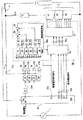
図3は、図1で示したアクティブフィルタに、電力変換装置3を駆動する制御装置の詳細構成を付加して図示したものである。制御装置は、電源電圧に基づいて出力電圧の基本階調を演算して基本階調信号18aを出力する基本階調演算部としてのCPU10(Central Processing Unit)と、CPU以外の外部回路で構成される。外部回路は、上記基本階調(基本階調信号18a)を補正するための階調補正値を演算して階調補正信号55aを出力する階調補正演算部と、上記基本階調を上記階調補正値(階調補正信号55a)にて補正して電力変換装置3の出力電圧階調指令56aを演算する出力階調演算回路56と、該出力電圧階調指令56aに基づいて各単相インバータ41〜43への制御信号を出力するインバータ制御演算回路57とを備える。
また、階調補正信号55aを出力する階調補正演算部は、電力変換装置3の出力電流(以下、インバータ電流Iaと称す)が、負荷電流ILに基づいて演算される高調波補償基準電流24aに追従するように階調補正信号55aを出力するもので、レベルシフト回路25〜28、ヒステリシスコンパレータとなるコンパレータ29〜32、マルチプレクサ33〜38、フリップフロップ51〜53、減算器54、および加算器55を備える。
Next, current control and operation of the harmonic compensation current by gradation control of the power conversion device 3 will be described.
FIG. 3 shows the active filter shown in FIG. 1 with a detailed configuration of a control device that drives the power conversion device 3 added. The control device includes a CPU 10 (Central Processing Unit) as a basic gradation calculation unit that calculates a basic gradation of an output voltage based on a power supply voltage and outputs a
The gradation correction operation unit for outputting a
電流センサ11にて検出された負荷電流ILは、バンドパスフィルタ13により高調波成分を除去して負荷電流ILの基本波成分を抽出し、入力端子15からCPU10に入力される。また、図示しない電圧センサにて検出された電源電圧は入力端子16からCPU10に入力される。これら入力データは、CPU10に内蔵されているADコンバータによってアナログ値からディジタル値に変換され、得られたディジタルデータをもとに信号処理を行う。CPU10の出力端子17からは離散系の負荷電流基本波成分をDAコンバータを介して出力する。また、電力変換装置3は電源電圧に同期した電圧を出力する必要があるため、ADコンバータで検出した電源電圧値を階段波形に置き換えて、出力端子18〜21から2進数(4ビット)で基本階調信号18aを出力し、同時に、出力端子22から電源電圧極性信号22aを出力する。
Load current I L is detected by the
CPU10の出力端子17から出力された負荷電流基本波成分は離散系であるため、フィルタ23で平滑し、減算器24を用いて、平滑された負荷電流基本波成分から負荷電流ILを減算することで、電力変換回路3に流すべき基準電流である高調波補償基準電流24aを生成する。
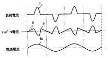
このように生成された高調波補償基準電流24aに追従するように、電圧変換装置3の出力電流であるインバータ電流Iaを制御することで、図4に示すように、負荷電流ILの高調波成分はインバータ電流Iaにより相殺され、正弦波形の電源電流ISが得られる。
Since the load current fundamental wave component output from the
So as to follow to the thus generated harmonic
インバータ電流Iaの制御について、以下に説明する。
図5は、図4のインバータ電流Ia波形におけるA部分を拡大した部分拡大図である。
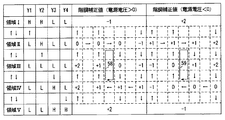
図3に示すように、生成された高調波補償基準電流24aに基づいて、レベルシフト回路25〜28を用いて、図5に示すような4つの閾値25a〜28a(閾値A、閾値B、閾値C、閾値D)を設定する。また、閾値Aより大きい領域を領域I、閾値Aと閾値Bとの間の領域を領域II、閾値Bと閾値Cとの間を領域III、閾値Cと閾値Dとの間を領域IV、閾値Dより小さい領域を領域Vとする。
インバータ電流Iaの制御としては、図5に示すように、インバータ電流Iaが領域IIIの範囲内、即ち、閾値Bと閾値Cとを往復するように、ヒステリシスコンパレータ30、31を用いて、電力変換装置3の出力電圧(出力電圧階調指令56a)を選択する。ここでは出力電圧階調指令56aとして、CPU10から出力される基本階調18aに階調補正値55aとして0もしくは+1を加算する。なお、この場合、CPU10から出力される基本階調18aは、図6に示すように電源電圧波形に内接するように整数部だけを絶対値で出力したものとする。これにより、電源電圧の極性が正の場合、階調補正値55aを0としてインバータ電流Iaを減少させ、階調補正値55aを+1としてインバータ電流Iaを増加させることができる。また、電源電圧の極性が負の場合は、階調補正値55aを0としてインバータ電流Iaを増加させ、階調補正値55aを+1としてインバータ電流Iaを減少させることができる。
For control of the inverter current I a, it will be described below.
Figure 5 is a partially enlarged view of A portion in the inverter current I a waveform of FIG.
As shown in FIG. 3, four
The control of the inverter current I a, as shown in FIG. 5, in the range inverter current I a is a region III, that is, so as to reciprocate the threshold value B and threshold value C, and using a
このような階調補正値55aの決定方法について、図3に基づいて以下に説明する。4つの閾値25a〜28a(閾値A、閾値B、閾値C、閾値D)と電流センサ12によって検出したインバータ電流Iaとをヒステリシスコンパレータ29〜32を用いて比較し、それぞれの出力信号をY1、Y2、Y3、Y4とする。図7に各領域におけるコンパレータ出力Y1〜Y4の値、および階調補正値を示す。コンパレータ出力Y1〜Y4はマルチプレクサ33〜38に図示するように入力される。マルチプレクサ33〜38には、電源電圧極性信号22aも入力され、電源電圧極性に応じて出力信号を切り替える。ここでは、電源電圧が正のときにはマルチプレクサ入力の上段が出力され、電源電圧が負のときにマルチプレクサ入力の下段が出力される。マルチプレクサ33〜38から出力された信号は、フリップフロップ回路51〜53に入力される。フリップフロップ回路51〜53はセット(S)、リセット(R)方式である。フリップフロップ回路51〜53の出力信号は減算器54および加算器55を通すことで階調補正値55aが得られる。なお、図3に破線で示した部分はPLD(Programmable Logic Device)などのデバイスを用いて実現することができる。
A method for determining the
一例として、電源電圧の極性が正の場合について、図7および図8を用いて説明する。図8は、CPU10から出力される基本階調18aがサンプリングによる遅れを伴わない正常時における、インバータ電流Iaと出力電圧(出力電圧階調指令56a)との関係を示すものである。
CPU10からの電源電圧極性信号22aにより、上述したようにマルチプレクサ33〜38では、マルチプレクサ入力の上段が出力される。ここで、インバータ電流Iaが減少し、領域IIIから領域IVへ移行するとする。このときコンパレータ31の出力信号Y3がLからHへと変化し、マルチプレクサ33からはH信号が出力される。この信号がフリップフロップ51のセット端子に入力され、出力端子(Q)からはH信号が出力される。このとき、階調補正値51aは+1となる。他のフリップフロップ52、53から出力される信号はLであり、減算器54および加算器55を通して、階調補正値55aは階調補正値51aの値である+1となる。
As an example, the case where the polarity of the power supply voltage is positive will be described with reference to FIGS. FIG. 8 shows the relationship between the inverter current Ia and the output voltage (output
As described above, the
この1階調分の階調補正によってインバータ電流Iaが減少から増加へ変化し、領域IIIの範囲であるとき、フリップフロップ51はセット端子、リセット端子共にLのため、出力信号はHのまま維持され、階調補正値55aは+1で1階調加算の状態が継続する。インバータ電流Iaが増加し続け領域IIIから領域IIへと移行するとき、コンパレータ30の出力信号Y2はLからHへと変化し、マルチプレクサ34からはH信号が出力される。この信号がフリップフロップ51のリセット端子に入力され、出力端子(Q)からはL信号が出力される。このとき、階調補正値51aは0となる。他のフリップフロップ52、53から出力される信号はLであり、減算器54および加算器55を通して、階調補正値55aは階調補正値51aの値である0となる。
階調補正値55aが0となると、インバータ電流Iaは減少する。インバータ電流Iaは領域IIIの範囲となり、フリップフロップ51はセット端子、リセット端子共にLとなるため、状態は保持され(階調補正値55aは0)、領域IVに移行するまで減少を続ける。その後は同様の原理で階調補正値55aが+1になり、インバータ電流Iaは増加の方向へ変化する。
Inverter current I a are changed to increase from decrease by the one gradation in the gradation correction, when a range of the area III, the flip-
When the
このように、階調補正値55aは、図7中の矢印58で示すように推移して、図8に示すように、基本階調18aに階調補正値55aである0もしくは+1を交互に加算した出力電圧階調指令56aを生成して、インバータ電流Iaを領域IIIの範囲内、即ち、閾値Bと閾値Cとを往復するように制御する。即ち、インバータ電流Iaが増加して閾値Bを超えると階調補正値55aを0としてインバータ電流Iaを減少させ、インバータ電流Iaが減少して閾値Cより小さくなると階調補正値55aを+1としてインバータ電流Iaを増加させる。閾値A〜Dは、その時点の高調波補償基準電流24aに基づいて生成されるので、インバータ電流Iaは、高調波補償基準電流24aに追従するように制御される。
In this way, the
電源電圧の極性が負の場合、CPU10からの電源電圧極性信号22aにより、上述したようにマルチプレクサ33〜38では、マルチプレクサ入力の下段が出力される。ここで、インバータ電流Iaが減少し、領域IIIから領域IVへ移行するとする。このときコンパレータ31の出力信号Y3がLからHへと変化し、マルチプレクサ34からH信号が出力される。この信号がフリップフロップ51のリセット端子に入力され、出力端子(Q)からはL信号が出力される。このとき、階調補正値51aは0となる。他のフリップフロップ52、53から出力される信号はLであり、減算器54および加算器55を通して、階調補正値55aは階調補正値51aの値である0となる。
When the polarity of the power supply voltage is negative, the
階調補正値55aが0になると、インバータ電流Iaが増加し、領域IIIの範囲であるとき、フリップフロップ51はセット端子、リセット端子共にLのため、出力信号はLのまま維持され、階調補正値55aは0の状態が継続する。インバータ電流Iaが増加し続け、領域IIIから領域IIへと移行するとき、コンパレータ30の出力信号Y2はLからHへと変化し、マルチプレクサ33からH信号が出力される。この信号がフリップフロップ51のセット端子に入力され、出力端子(Q)からはH信号が出力される。このとき、階調補正値51aは+1となる。他のフリップフロップ52、53から出力される信号はLであり、減算器54および加算器55を通して、階調補正値55aは階調補正値51aの値である+1となる。
When the
階調補正値55aが+1となると、インバータ電流Iaは減少する。インバータ電流Iaは領域IIIの範囲となり、フリップフロップ51はセット端子、リセット端子共にHとなるため、状態は保持され(階調補正値55aは+1)、領域IVに移行するまでインバータ電流Iaは減少を続ける。その後は同様の原理で階調補正値55aが0になり、インバータ電流Iaは増加の方向へ変化する。
このように、階調補正値55aは、図7中の矢印59で示すように推移して、基本階調18aに階調補正値55aである0もしくは+1を交互に加算した出力電圧階調指令56aを生成して、インバータ電流Iaを領域IIIの範囲内、即ち、閾値Bと閾値Cとを往復するように制御する。
When the
In this way, the
CPU10から出力される基本階調18aがADコンバータのサンプリング間隔の影響による遅れで誤った階調値を出力した場合には、インバータ電流Iaは階調補正を行っても、領域IIIから領域IIあるいは領域IVの範囲に外れてしまう。このように基本階調出力に遅れがある場合の制御について以下に説明する。
電源電圧の極性が正で、インバータ電流Iaが領域IIIから領域IVに移行したときは、先に説明したように、階調補正値55aが+1になる。このとき、CPU10から出力される基本階調18aに1階調が加算される。しかし、電源電圧の時間変化率が正のとき、サンプリングに時間遅れが生じると、階調値が不足するときがある。このときのインバータ電流Iaと出力電圧(出力電圧階調指令56a)との関係について、図9に示す。
When the
In the polarity of the supply voltage is positive, when the inverter current I a is shifted from the region III to region IV, as described above, the
図9に示すように、電圧変化率が正の場合は、基本階調値切替タイミングが遅れているため、切り換えるべき時点61以降の遅れ時間の間は、インバータ電流Iaが減少して閾値Cより小さくなった時点62で階調補正値55aを+1としても、出力電圧階調指令56aが電源電圧より不足しているためインバータ電流Iaが減少し続ける。そして、閾値Dより小さくなる時点63で、即ち、インバータ電流Iaが領域IVから領域Vに移行するとコンパレータ32からH信号が出力され、マルチプレクサ37からH信号が出力される。この信号がフリップフロップ53のセット端子に入力され、出力端子(Q)からはH信号が出力される。この信号は、CPU10からの基本階調18aの出力遅れを補正するための階調ずれ補正値53aであり、加算器55によって階調補正値51aに加えられる。この場合、階調補正値51a(+1)に階調ずれ補正値53a(+1)を加算して、階調補正値55aは+2となる。
As shown in FIG. 9, when the voltage change rate is positive, the basic gradation value switching timing is delayed. Therefore, during the delay time after the time point 61 to be switched, the inverter current Ia decreases and the threshold value C even +1
その後、インバータ電流Iaは増加の方向へ変化し、領域Vから領域IVへ移行すると、マルチプレクサ37の出力はLとなり、フリップフロップ53はセット端子、リセット端子共にLとなるため、状態は保持され(階調補正値55aは+2)、インバータ電流Iaは増加し続ける。領域IVから領域IIIに移行するとコンパレータ31の出力信号はHからLへと変化する。フリップフロップ53はセット端子、リセット端子共にLとなるため、状態は保持され(階調補正値55aは+2)、領域IIへ移行するまで、インバータ電流Iaは増加を続ける。そして、インバータ電流Iaが領域IIIから領域IIへ移行するとコンパレータ30の出力信号Y2はLからHへと変化し、マルチプレクサ34およびマルチプレクサ38からH信号が出力される。この信号がフリップフロップ51およびフリップフロップ53のリセット端子に入力され、フリップフロップ51およびフリップフロップ53の出力端子(Q)からはともにL信号が出力される。つまり、階調補正値51a(0)に階調ずれ補正値53a(0)を加算して、階調補正値55aは0となる。その後、インバータ電流Iaは減少の方向へ変化する。そして、基本階調出力が正しい値となるまで同様の原理で補正を行う。
Thereafter, the inverter current I a is changed to increase direction, the transition from the region V to the region IV, the output of the
電源電圧の極性が正で電圧変化率が負のとき、サンプリングに時間遅れが生じると、CPU10からの基本階調18aは電源電圧と内接するように整数値を出力しているため、階調値が1階調多く出力されるときがある。このときのインバータ電流Iaと出力電圧(出力電圧階調指令56a)との関係について、図10に示す。
図10に示すように、電圧変化率が負の場合は、基本階調値切替タイミングが遅れているため、切り換えるべき時点61a以降の遅れ時間の間は、インバータ電流Iaが増加して閾値Bを超えた時点62aで階調補正値55aを0としても、出力電圧階調指令56aが電源電圧より大きいためインバータ電流Iaが増加し続ける。このため、閾値Aを超える時点63aで、即ち、インバータ電流Iaが領域IIから領域Iへと移行すると、コンパレータ29からH信号が出力され、マルチプレクサ35からH信号が出力される。この信号がフリップフロップ52のセット端子に入力され、出力端子(Q)からはH信号が出力される。この信号は、CPU10からの基本階調18aの出力遅れを補正するための階調ずれ補正値52aであり、減算器54によって階調補正値51aから減算される。この場合、階調補正値51a(0)から階調ずれ補正値52a(+1)を減算して、階調補正値55aは−1となる。
When the polarity of the power supply voltage is positive and the voltage change rate is negative, if a time delay occurs in sampling, the
As shown in FIG. 10, when the voltage change rate is negative, the basic gradation value switching timing is delayed. Therefore, the inverter current Ia increases during the delay time after the time point 61a to be switched, and the threshold value B also the
その後、インバータ電流Iaが増加から減少の方向へ変化し、領域Iから領域IIに変化し、領域IIの範囲であるとき、フリップフロップ52はセット端子、リセット端子共にLのため、出力信号はHのまま維持され、状態は保持され(階調補正値55aは−1)て、インバータ電流Iaが減少し続ける。インバータ電流Iaが領域IIから領域IIIへと移行するとき、コンパレータ30の出力信号はHからLへと変化する。フリップフロップ51およびフリップフロップ53はセット端子、リセット端子共にLのため、出力信号はLのまま維持され、階調補正値55aは−1の状態が継続する。さらにインバータ電流Iaが減少し続け、領域IIIから領域IVへと移行するとき、コンパレータ31の出力信号はLからHへと変化し、マルチプレクサ33からH信号が出力される。この信号がフリップフロップ51のセット端子に入力され、出力端子(Q)からはH信号が出力される。さらに、マルチプレクサ36からH信号が出力され、フリップフロップ52のリセット端子に入力される。したがって階調補正値51a(+1)から階調ずれ補正値52a(0)を減算して、階調補正値55aは+1となる。
その後は同様の原理でインバータ電流Iaが領域IIIの範囲で増減するように階調補正を行う。
Thereafter, changes from the inverter current I a is increased in the direction of decreasing varies from region I to region II, when a range of the area II, the flip-
Then performs tone correction to the inverter current I a is increased or decreased in a range of area III in the same principle.
以上のように決定された階調補正値55aは、CPU10外部のディジタル回路である出力階調演算回路56にて、基本階調18aに加算されて出力電圧階調指令56aが出力される。この出力電圧階調指令56aは、インバータ制御演算回路57に入力されて、各単相インバータ4のゲート駆動回路81〜84へ送る制御信号を送出する。インバータ制御演算回路57は、PLD(Programmable Logic Device)などのデバイスを用いて実現することができる。
The
この実施の形態では、複数の単相インバータ41〜43を直列接続した電力変換装置3をアクティブフィルタに用い、各単相インバータ41〜43の出力電圧を適宜選択する階調制御により、所望の階段波形の出力電圧を得て、インバータ電流Iaを制御するため、フィルタ回路5を格段と小型化でき、アクティブフィルタの装置構成の小型化が促進できる。
また、インバータ電流Iaを高調波補償基準電流24aに追従するように制御するのに、制御装置は、電源電圧に基づいて出力電圧の基本階調18aを出力する基本階調演算部のみをCPU10で構成し、階調補正信号55aを出力する階調補正演算部と、電力変換装置3の出力電圧階調指令56aを演算する出力階調演算回路56と、各単相インバータ41〜43への制御信号を出力するインバータ制御演算回路57とは、CPU以外の外部回路で構成した。このため、CPU10の負担を軽減させることができ、安価なCPU10でも対応可能となり、制御装置のコスト低減が図れる。また、階調補正信号55aを出力する階調補正演算部では、ヒステリシスコンパレータ29〜32を用い、高速、高精度に、インバータ電流Iaを高調波補償基準電流に追従するように制御できる。また、CPU10のサンプリング間隔が比較的大きい場合でも、階調ずれ補正値52a、53aを演算して補正できるようにしたため、安価なCPU10でも、高速、高精度で信頼性の高い高調波抑制制御が行える。
In this embodiment, the power conversion device 3 in which a plurality of single-
Further, to control so as to follow the inverter current I a harmonic compensation reference current 24a, the control device, the basic tone calculation unit for outputting a
なお、この実施の形態では、CPU10からの基本階調18aは電源電圧の正弦波に内接するように整数部だけを出力したが、図11で示すように、電源電圧の正弦波に外接するように階調値を出力しても良い。この場合、階調補正値は、内接させた場合の階調補正値55aから1を引けば良い。このように、基本階調18aを、電源電圧の正弦波に内接あるいは、外接させるように出力することにより、階調補正値55aの演算が容易になり、インバータ電流Iaを高調波補償基準電流に追従させる電流制御が容易で信頼性良く行える。
In this embodiment, the
また、ヒステリシスコンパレータ29〜32の閾値幅の設定については、電源電流のリプルが許容される範囲内となるように設定する。電流リプルを小さくするには、ヒステリシスコンパレータ29〜32の閾値幅を小さく設定すれば良いが、スイッチング素子71〜74の周波数が高くなる。このように、電流制御精度とスイッチング周波数との関係は、トレードオフの関係となることから、ヒステリシスコンパレータ29〜32の閾値幅は、一段あたりの階調電圧値、および単相インバータ4を構成するスイッチング素子71〜74の許容される最大スイッチング周波数から決定される。また、電流の変化率については、電源インピーダンス、およびフィルタ回路4のリアクトルの大きさによって異なるため、電源電流のリプルが許容される範囲内となるようにフィルタリアクトルの設計を行う。
Further, the threshold widths of the
実施の形態2.
上記実施の形態1では、インバータ電流Iaを高調波補償基準電流24aに追従するように制御したが、図12に示すように、CPU10から出力された離散系の負荷電流基本波成分をフィルタ23で平滑した基準電流(負荷電流基本波成分)に追従するように、電源電流ISを制御しても良い。
なお、上記実施の形態1では、負荷電流ILは、バンドパスフィルタ13により高調波成分を除去して負荷電流ILの基本波成分を抽出してCPU10に入力したが、この場合、CPU10内で負荷電流ILの基本波成分を抽出するようにした。
この場合も、実際には電力変換装置3の出力階調制御により、インバータ電流Iaを変化させて電源電流ISを制御しているため、結果的には上記実施の形態1と同様に、インバータ電流Iaが高調波成分を打ち消す高調波補償基準電流に追従するように制御されるものとなり、上記実施の形態1と同様の効果が得られる。
In the first embodiment, the inverter current was controlled to the I a to follow the harmonic compensation reference current 24a, as shown in FIG. 12, the
Although in the above-mentioned first embodiment, the load current I L has been to remove the harmonic component input to CPU10 extracts a fundamental wave component of the load current I L through the band-
Again, the fact the output tone control of the power converter 3, since by changing the inverter current I a and controls the source current I S, similar to the first embodiment is consequently, The inverter current Ia is controlled to follow the harmonic compensation reference current that cancels the harmonic component, and the same effect as in the first embodiment can be obtained.
1 電源、2 負荷、3 電力変換装置、4(41〜43) 単相インバータ、
6 直流電源、10 CPU、18a 基本階調信号、24a 高調波補償基準電流、
25a〜28a 閾値A〜D、29〜32 ヒステリシスコンパレータ、
51a 階調補正値、52a,53a 階調ずれ補正値、54 減算器、55 加算器、55a 階調補正信号、56 出力階調演算回路、57 インバータ制御演算回路、
71〜74 スイッチング素子、IL 負荷電流、Ia インバータ電流。
1 power supply, 2 load, 3 power converter, 4 (41-43) single-phase inverter,
6 DC power supply, 10 CPU, 18a basic gradation signal, 24a harmonic compensation reference current,
25a to 28a threshold A to D, 29 to 32 hysteresis comparator,
51a gradation correction value, 52a, 53a gradation deviation correction value, 54 subtractor, 55 adder, 55a gradation correction signal, 56 output gradation calculation circuit, 57 inverter control calculation circuit,
71-74 switching elements, I L the load current, I a inverter current.
Claims (8)
上記制御装置は、与えられた基準電圧に基づいて上記出力電圧の基本階調を演算する基本階調演算部と、上記出力電流が設定された目標電流に追従するように上記基本階調を補正するための階調補正値を演算する階調補正演算部と、上記基本階調を上記階調補正値にて補正して上記単相インバータ群の出力電圧階調を演算する出力階調演算部と、上記出力電圧階調に基づいて上記単相インバータ群への制御信号を出力するインバータ制御演算部とを備え、 The control device corrects the basic gradation so that the basic gradation calculation unit for calculating the basic gradation of the output voltage based on a given reference voltage and the output current follows a set target current. And a gradation correction calculation unit for calculating a gradation correction value for calculating the output voltage gradation of the single-phase inverter group by correcting the basic gradation with the gradation correction value. And an inverter control operation unit that outputs a control signal to the single-phase inverter group based on the output voltage gradation,
上記階調補正演算部は、上記出力電流に複数の閾値を設け、各閾値を越える毎に上記階調補正値を変化させて上記出力電圧階調を変化させることを特徴とする電力変換装置。 The power conversion apparatus according to claim 1, wherein the gradation correction calculation unit provides a plurality of threshold values for the output current, and changes the output voltage gradation by changing the gradation correction value every time the threshold value is exceeded.
上記制御装置は、上記交流電源の電源電圧に基づいて上記出力電圧の基本階調を演算する基本階調演算部と、上記出力電流が目標電流に追従するように上記基本階調を補正するための階調補正値を演算する階調補正演算部と、上記基本階調を上記階調補正値にて補正して上記単相インバータ群の出力電圧階調を演算する出力階調演算部と、上記出力電圧階調に基づいて上記単相インバータ群への制御信号を出力するインバータ制御演算部とを備え、 The control device corrects the basic gradation so that the output gradation follows a target current, and a basic gradation calculator that calculates a basic gradation of the output voltage based on a power supply voltage of the AC power supply A gradation correction calculation unit that calculates the gradation correction value of the output, an output gradation calculation unit that calculates the output voltage gradation of the single-phase inverter group by correcting the basic gradation with the gradation correction value, An inverter control operation unit that outputs a control signal to the single-phase inverter group based on the output voltage gradation,
上記階調補正演算部は、上記出力電流に複数の閾値を設け、各閾値を越える毎に上記階調補正値を変化させて上記出力電圧階調を変化させることを特徴とする電力変換装置。 The power conversion apparatus according to claim 1, wherein the gradation correction calculation unit provides a plurality of threshold values for the output current, and changes the output voltage gradation by changing the gradation correction value every time the threshold value is exceeded.
Priority Applications (1)
| Application Number | Priority Date | Filing Date | Title |
|---|---|---|---|
| JP2004255286A JP4234082B2 (en) | 2004-09-02 | 2004-09-02 | Power converter |
Applications Claiming Priority (1)
| Application Number | Priority Date | Filing Date | Title |
|---|---|---|---|
| JP2004255286A JP4234082B2 (en) | 2004-09-02 | 2004-09-02 | Power converter |
Related Child Applications (1)
| Application Number | Title | Priority Date | Filing Date |
|---|---|---|---|
| JP2008257164A Division JP5154359B2 (en) | 2008-10-02 | 2008-10-02 | Power converter |
Publications (3)
| Publication Number | Publication Date |
|---|---|
| JP2006074905A JP2006074905A (en) | 2006-03-16 |
| JP2006074905A5 JP2006074905A5 (en) | 2007-04-26 |
| JP4234082B2 true JP4234082B2 (en) | 2009-03-04 |
Family
ID=36154898
Family Applications (1)
| Application Number | Title | Priority Date | Filing Date |
|---|---|---|---|
| JP2004255286A Active JP4234082B2 (en) | 2004-09-02 | 2004-09-02 | Power converter |
Country Status (1)
| Country | Link |
|---|---|
| JP (1) | JP4234082B2 (en) |
Families Citing this family (5)
| Publication number | Priority date | Publication date | Assignee | Title |
|---|---|---|---|---|
| CN100459361C (en) * | 2006-12-01 | 2009-02-04 | 山东山大华天科技股份有限公司 | Hybrid active power filter and its control method |
| CN102623997B (en) * | 2012-03-28 | 2014-04-09 | 江苏大学 | Method for realizing feedback linearization double hysteresis composite controller of active power filter |
| CN105305449B (en) * | 2015-11-26 | 2018-01-09 | 上海艾临科智能科技有限公司 | Shipping shore power system |
| SG11201912049PA (en) * | 2017-06-12 | 2020-01-30 | Tae Technologies Inc | Multi-level multi-quadrant hysteresis current controllers and methods for control thereof |
| CN112087003B (en) * | 2020-08-27 | 2022-06-03 | 国网电力科学研究院有限公司 | New energy centralized frequency correction control system and control method |
-
2004
- 2004-09-02 JP JP2004255286A patent/JP4234082B2/en active Active
Also Published As
| Publication number | Publication date |
|---|---|
| JP2006074905A (en) | 2006-03-16 |
Similar Documents
| Publication | Publication Date | Title |
|---|---|---|
| EP3062428B1 (en) | Inverter phase current reconstruction apparatus and methods | |
| KR100655917B1 (en) | PWM Pulse Control Method | |
| US10153712B2 (en) | Circulating current injection control | |
| US8817499B2 (en) | Control method and system for reducing the common-mode current in a power converter | |
| WO2007129456A1 (en) | Power converter | |
| JP5154359B2 (en) | Power converter | |
| JP6134733B2 (en) | Polyphase converter system and method | |
| US9705422B2 (en) | System and method for soft switching power inversion | |
| JP2006238630A (en) | Power conversion device | |
| JP6396135B2 (en) | Power converter | |
| JP4234082B2 (en) | Power converter | |
| JP2010068630A (en) | Inverter control circuit, system linkage inverter system having same, program for achieving same, and recording medium recording program | |
| JP2023099680A (en) | Power conversion device | |
| JP6946041B2 (en) | Power converter | |
| JP6303908B2 (en) | Neutral point potential control method for single-phase NPC inverter | |
| JP2008048537A (en) | Ac-ac power conversion apparatus | |
| JP4498891B2 (en) | Semiconductor power converter | |
| JP5154587B2 (en) | Power converter | |
| JP3053945B2 (en) | Neutral point clamp type power converter controller | |
| JP2008295135A (en) | Power conversion equipment | |
| JP2015035869A (en) | Multi-level power converting device and multi-level power converting device control method | |
| JP4448294B2 (en) | Power converter | |
| JPH1052062A (en) | Controller for three-level inverter | |
| JP2013188007A (en) | Power converter | |
| JPWO2017034028A1 (en) | Inverter control method |
Legal Events
| Date | Code | Title | Description |
|---|---|---|---|
| A621 | Written request for application examination |
Free format text: JAPANESE INTERMEDIATE CODE: A621 Effective date: 20061031 |
|
| A521 | Request for written amendment filed |
Free format text: JAPANESE INTERMEDIATE CODE: A523 Effective date: 20070313 |
|
| A977 | Report on retrieval |
Free format text: JAPANESE INTERMEDIATE CODE: A971007 Effective date: 20080728 |
|
| A131 | Notification of reasons for refusal |
Free format text: JAPANESE INTERMEDIATE CODE: A131 Effective date: 20080805 |
|
| A521 | Request for written amendment filed |
Free format text: JAPANESE INTERMEDIATE CODE: A523 Effective date: 20081002 |
|
| TRDD | Decision of grant or rejection written | ||
| A01 | Written decision to grant a patent or to grant a registration (utility model) |
Free format text: JAPANESE INTERMEDIATE CODE: A01 Effective date: 20081209 |
|
| A01 | Written decision to grant a patent or to grant a registration (utility model) |
Free format text: JAPANESE INTERMEDIATE CODE: A01 |
|
| A61 | First payment of annual fees (during grant procedure) |
Free format text: JAPANESE INTERMEDIATE CODE: A61 Effective date: 20081210 |
|
| FPAY | Renewal fee payment (event date is renewal date of database) |
Free format text: PAYMENT UNTIL: 20111219 Year of fee payment: 3 |
|
| R150 | Certificate of patent or registration of utility model |
Ref document number: 4234082 Country of ref document: JP Free format text: JAPANESE INTERMEDIATE CODE: R150 Free format text: JAPANESE INTERMEDIATE CODE: R150 |
|
| FPAY | Renewal fee payment (event date is renewal date of database) |
Free format text: PAYMENT UNTIL: 20111219 Year of fee payment: 3 |
|
| FPAY | Renewal fee payment (event date is renewal date of database) |
Free format text: PAYMENT UNTIL: 20121219 Year of fee payment: 4 |
|
| FPAY | Renewal fee payment (event date is renewal date of database) |
Free format text: PAYMENT UNTIL: 20121219 Year of fee payment: 4 |
|
| FPAY | Renewal fee payment (event date is renewal date of database) |
Free format text: PAYMENT UNTIL: 20131219 Year of fee payment: 5 |
|
| R250 | Receipt of annual fees |
Free format text: JAPANESE INTERMEDIATE CODE: R250 |
|
| R250 | Receipt of annual fees |
Free format text: JAPANESE INTERMEDIATE CODE: R250 |
|
| R250 | Receipt of annual fees |
Free format text: JAPANESE INTERMEDIATE CODE: R250 |
|
| R250 | Receipt of annual fees |
Free format text: JAPANESE INTERMEDIATE CODE: R250 |
|
| R250 | Receipt of annual fees |
Free format text: JAPANESE INTERMEDIATE CODE: R250 |
|
| R250 | Receipt of annual fees |
Free format text: JAPANESE INTERMEDIATE CODE: R250 |
|
| R250 | Receipt of annual fees |
Free format text: JAPANESE INTERMEDIATE CODE: R250 |
|
| R250 | Receipt of annual fees |
Free format text: JAPANESE INTERMEDIATE CODE: R250 |
|
| R250 | Receipt of annual fees |
Free format text: JAPANESE INTERMEDIATE CODE: R250 |