JP4227516B2 - 容量式センサ並びに容量式センサの製造方法 - Google Patents
容量式センサ並びに容量式センサの製造方法 Download PDFInfo
- Publication number
- JP4227516B2 JP4227516B2 JP2003514583A JP2003514583A JP4227516B2 JP 4227516 B2 JP4227516 B2 JP 4227516B2 JP 2003514583 A JP2003514583 A JP 2003514583A JP 2003514583 A JP2003514583 A JP 2003514583A JP 4227516 B2 JP4227516 B2 JP 4227516B2
- Authority
- JP
- Japan
- Prior art keywords
- electrode
- layer
- porous layer
- medium
- capacitive sensor
- Prior art date
- Legal status (The legal status is an assumption and is not a legal conclusion. Google has not performed a legal analysis and makes no representation as to the accuracy of the status listed.)
- Expired - Fee Related
Links
Images


Classifications
-
- G—PHYSICS
- G01—MEASURING; TESTING
- G01N—INVESTIGATING OR ANALYSING MATERIALS BY DETERMINING THEIR CHEMICAL OR PHYSICAL PROPERTIES
- G01N27/00—Investigating or analysing materials by the use of electric, electrochemical, or magnetic means
- G01N27/02—Investigating or analysing materials by the use of electric, electrochemical, or magnetic means by investigating impedance
- G01N27/04—Investigating or analysing materials by the use of electric, electrochemical, or magnetic means by investigating impedance by investigating resistance
- G01N27/12—Investigating or analysing materials by the use of electric, electrochemical, or magnetic means by investigating impedance by investigating resistance of a solid body in dependence upon absorption of a fluid; of a solid body in dependence upon reaction with a fluid, for detecting components in the fluid
- G01N27/121—Investigating or analysing materials by the use of electric, electrochemical, or magnetic means by investigating impedance by investigating resistance of a solid body in dependence upon absorption of a fluid; of a solid body in dependence upon reaction with a fluid, for detecting components in the fluid for determining moisture content, e.g. humidity, of the fluid
Landscapes
- Chemical & Material Sciences (AREA)
- Chemical Kinetics & Catalysis (AREA)
- Electrochemistry (AREA)
- Physics & Mathematics (AREA)
- Health & Medical Sciences (AREA)
- Life Sciences & Earth Sciences (AREA)
- Analytical Chemistry (AREA)
- Biochemistry (AREA)
- General Health & Medical Sciences (AREA)
- General Physics & Mathematics (AREA)
- Immunology (AREA)
- Pathology (AREA)
- Investigating Or Analyzing Materials By The Use Of Electric Means (AREA)
- Investigating Or Analyzing Materials By The Use Of Fluid Adsorption Or Reactions (AREA)
Description
本発明は、該当する独立請求項の上位概念に記載された半導体構成素子、例えば特に湿度センサ、および半導体構成素子の製造方法に関する。
該当する独立請求項に記載された特徴部分の構成を有する本発明による半導体構成素子はこれに対して、低コストで製造可能な、孔が設けられた層を有しているという利点を有する。この層内に質的および/または量的に突き止められるべき媒体が達し、これによって多孔性の層の誘電数が変化する。このような層は有利には孔が設けられたシリコン層ないし多孔性のシリコン層である。ポリマー層が設けられている公知の容量性湿度センサと異なり、本発明による多孔性の層は湿度に依存する膨張(Aufquellen)を示さない。
本発明による半導体構成素子と、本発明による半導体構成素子の製造方法を以下で湿度センサの例に即してより詳細に説明する。ここでは概略的な、必ずしも尺度は正確でない図面を用いる。ここで同一の、または同じ作用をする層または部分には同じ参照番号が付されている。
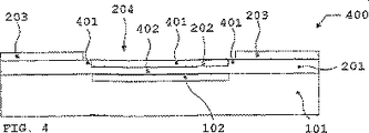
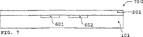
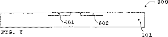
101 シリコン基板
102 適切なドーピング領域によって作成された底面電極、下部電極
103 上部エッチングされたポリマー層
104 構造化された被覆電極、上部電極
200 本発明による湿度センサの第1の実施形態に対する製造段階物
201 シリコン中間層
202 被覆電極、上部電極、ドーピング領域
203 マスク層
204 エッチング開口部
300 図2に示された第1の実施形態に対する第1の形態
301 エッチング開口部204の下の全体領域において底面電極102まで延在している、中間層201内の多孔性の領域
400 図2に示された第1の実施形態に対する第2の形態
401 エッチング開口部204下の領域においてほぼ被覆電極202の下側まで延在している、より低い気孔率を有する領域
402 エッチング開口部204下の領域においてほぼ底面電極102の下側まで延在している、領域401に関してより高い気孔率を有している領域
500 電気的接続部が設けられた図3または図4の湿度センサに対する実施例の断面図並びに平面図
501 貫通接触接続部
502 底面電極を接続するコンタクト面
503 被覆電極の接触のためのコンタクト面
504 被覆電極の接触のためのコンタクト路
600 同じ高さに配置された2つの電極とその上に設けられた遮蔽電極を有する、本発明による湿度センサの第2の実施形態に対する第1の形態
601 第1の底面電極
602 第2の底面電極
603 遮蔽電極
700 遮蔽電極を有していない、図6に示された本発明による湿度センサ
800 遮蔽電極および中間層を有していない、図6に示された本発明による湿度センサ
900 プレートコンデンサの形をした、図6〜図8に示された電極に対する第1の実施形態
901 第1の底面電極
902 第2の底面電極
1000 相互にかみ合っている2つの櫛形電極によって作成されたインターデジタル構造体の形をした、図6〜図8に示された電極に対する第2の実施形態
1001 櫛の形をした第1の底面電極
1002 櫛の形をした第1の底面電極
1100 ネット状電極ないしは格子状電極を有する本発明による湿度センサの別の実施形態の例
1101 p型ドープされたシリコン基板
1102 p型ドープされたシリコン中間層
1103 ネット状の下部電極
1104 ネット状の上部電極
Claims (12)
- 半導体基板(101)と、第1の電極(102)と、第2の電極(202)と、第1の層(201)を有する容量式センサであって、
前記第1の層(201)は、半導体構成素子に外部から作用する媒体に対して、進入可能であり、
前記第1の層(201)は、少なくとも部分的に前記第1の電極と第2の電極の間に配置されており、
第1の多孔性層である前記第1の層(201)は孔(301)を有しており、当該孔に前記媒体が少なくとも部分的に達する形成の容量式センサにおいて、
少なくとも1つの電極(102,202)はドーピングされた半導体層によって構成されており、
前記第2の電極(202)は第2の多孔性層(401)であり、当該第2の多孔性層(401)を通じて前記媒体が前記第1の多孔性層(201)に達し、
前記第2の多孔性層(401)の気孔率、すなわち材料に対する孔の体積の割合は、前記第1の多孔性層(201)の気孔率より低い、
ことを特徴とする容量式センサ。 - 前記媒体は、湿気を有している空気のような気体または液体である、請求項1記載の容量式センサ。
- 前記半導体基板(101)はシリコンから成る、請求項1記載の容量式センサ。
- 前記第1の電極および第2の電極(601, 602)は実質的に同じ高さに、相互に間隔を有して配置されている、請求項1から3までのいずれか1項記載の容量式センサ。
- 前記第1の電極および第2の電極(1001, 1002)はインターデジタル構造体(1000)を構成している、請求項1から4までのいずれか1項記載の容量式センサ。
- 前記第1および/または第2の電極(102, 202)および/または前記第1の多孔性の層(301)は、第3の多孔性の層(603)によって覆われている、ないし保護されている、請求項1から5までのいずれか1項記載の容量式センサ。
- 前記容量式センサは湿度センサ(200,300,400,500,600,700,800)をあらわす、請求項1から6までのいずれか1項記載の容量式センサ。
- 容量式センサの製造方法であって、
第1の電極(102)と第2の電極(202)との間に少なくとも部分的に配置されている第1の層(201)である第1の多孔性の層(201)を少なくとも1つのエッチング媒体によるエッチングによって作成し、
当該第1の層(201)は、半導体構成素子に外部から作用する媒体に対して進入可能であり、孔(301)を有しており、当該孔に前記媒体が少なくとも部分的に達し、
少なくとも1つの電極(102,202)を作成するために半導体層をドーピングし、前記ドーピングされた半導体層をエッチングすることによって前記第2の電極(202)を第2の多孔性層(401)に作り変え、当該第2の多孔性層(401)を通じて前記媒体が前記第1の多孔性層(201)に達し、
前記第2の多孔性層(401)の気孔率、すなわち材料に対する孔の体積の割合は、前記第1の多孔性層(201)の気孔率より低く、
前記第1および第2の多孔性層(201 , 401)を、半導体構成素子の上側と下側との間で電界をかけ、かつ前記エッチング媒体を流れる電流を調整して作成する、
ことを特徴とする、容量式センサの製造方法。 - 前記エッチング媒体は少なくとも部分的にフッ酸から成る、請求項8記載の方法。
- 前記エッチング媒体は少なくとも添加物を有しており、
当該添加物はブリスター形成を減少させるための添加物、湿れ性を改善するための添加物および/または乾燥を改善するための添加物である、請求項8記載の方法。 - 添加物として、エタノールを使用し、当該添加物の体積濃度は約30%〜約90%である、請求項10記載の方法。
- 前記第1および/または第2の多孔性の層(201, 401)の気孔率の程度および/または前記第1および/または第2の多孔性の層の孔の拡大を、プロセスパラメータ、すなわち前記エッチング媒体における電流密度、前記エッチング媒体におけるフッ酸濃度、前記エッチング媒体への添加物、温度、ドーピング、電流の持続時間のうちの1つまたは複数を変えることによって制御する、請求項8から11までのいずれか1項記載の方法。
Applications Claiming Priority (2)
| Application Number | Priority Date | Filing Date | Title |
|---|---|---|---|
| DE10134938A DE10134938A1 (de) | 2001-07-18 | 2001-07-18 | Halbleiterbauelement sowie ein Verfahren zur Herstellung des Halbleiterbauelements |
| PCT/DE2002/002481 WO2003009334A2 (de) | 2001-07-18 | 2002-07-06 | Halbleiterbauelement als kapazitiver feuchtesensor, sowie ein verfahren zur herstellung des halbleiterbauelements |
Publications (3)
| Publication Number | Publication Date |
|---|---|
| JP2004535589A JP2004535589A (ja) | 2004-11-25 |
| JP2004535589A5 JP2004535589A5 (ja) | 2005-12-22 |
| JP4227516B2 true JP4227516B2 (ja) | 2009-02-18 |
Family
ID=7692211
Family Applications (1)
| Application Number | Title | Priority Date | Filing Date |
|---|---|---|---|
| JP2003514583A Expired - Fee Related JP4227516B2 (ja) | 2001-07-18 | 2002-07-06 | 容量式センサ並びに容量式センサの製造方法 |
Country Status (6)
| Country | Link |
|---|---|
| US (1) | US7193290B2 (ja) |
| EP (1) | EP1412732B1 (ja) |
| JP (1) | JP4227516B2 (ja) |
| AT (1) | ATE329255T1 (ja) |
| DE (2) | DE10134938A1 (ja) |
| WO (1) | WO2003009334A2 (ja) |
Families Citing this family (22)
| Publication number | Priority date | Publication date | Assignee | Title |
|---|---|---|---|---|
| US6931003B2 (en) * | 2000-02-09 | 2005-08-16 | Bookline Flolmstead Llc | Packet prioritization protocol for a large-scale, high speed computer network |
| US7110629B2 (en) * | 2002-07-22 | 2006-09-19 | Applied Materials, Inc. | Optical ready substrates |
| WO2004106987A2 (en) * | 2003-05-29 | 2004-12-09 | Applied Materials, Inc. | Impurity-based waveguide detectors |
| CN1856860A (zh) * | 2003-05-29 | 2006-11-01 | 应用材料股份有限公司 | 埋置式波导检测器 |
| US7205624B2 (en) * | 2003-10-07 | 2007-04-17 | Applied Materials, Inc. | Self-aligned implanted waveguide detector |
| US7368312B1 (en) * | 2004-10-15 | 2008-05-06 | Morgan Research Corporation | MEMS sensor suite on a chip |
| ITMO20050159A1 (it) * | 2005-06-22 | 2006-12-23 | Angelo Grandi Cucine Societa P | Sistema per il controllo dell'umidita'. |
| WO2007027615A1 (en) * | 2005-09-01 | 2007-03-08 | Applied Materials, Inc. | Ridge technique for fabricating an optical detector and an optical waveguide |
| CN101310175A (zh) * | 2005-11-17 | 2008-11-19 | Nxp股份有限公司 | 湿度传感器 |
| US7710128B2 (en) * | 2006-09-09 | 2010-05-04 | Honeywell International Inc. | Method and apparatus for controlling the sensitivity and value of a capacitive humidity sensor |
| DE202008003354U1 (de) | 2008-03-09 | 2008-05-15 | Hidde, Axel R., Dr. Ing. | Leckageüberwachung bei zylindrischen Anordnungen |
| KR101093612B1 (ko) | 2008-11-12 | 2011-12-15 | 전자부품연구원 | 정전용량형 습도센서 및 그 제조방법 |
| EP2336757B1 (en) * | 2009-12-07 | 2018-09-19 | ams international AG | Integrated circuit with water presence detection arrangement and manufacturing method therefor |
| CN103119429B (zh) * | 2010-05-06 | 2016-01-20 | 首尔大学校产学协力团 | 电容性元件传感器及其制造方法 |
| EP2693207A1 (en) * | 2012-07-30 | 2014-02-05 | Nxp B.V. | Integrated circuit comprising a capacitive gas sensor |
| DE102012108997A1 (de) * | 2012-09-24 | 2014-03-27 | Heinrich-Heine-Universität Düsseldorf | Sensoranordnung und Verfahren zum Herstellen einer Sensoranordnung |
| US8815054B2 (en) | 2012-10-05 | 2014-08-26 | The Procter & Gamble Company | Methods for making fibrous paper structures utilizing waterborne shape memory polymers |
| US9588073B2 (en) | 2012-12-19 | 2017-03-07 | Robert Bosch Gmbh | Resistive MEMS humidity sensor |
| EP2988122B1 (en) * | 2014-08-20 | 2019-04-24 | ams international AG | Capacitive sensor |
| TWI601954B (zh) * | 2016-09-09 | 2017-10-11 | 長庚大學 | 電容式感濕元件及其使用方法 |
| KR102007446B1 (ko) * | 2018-05-21 | 2019-10-21 | 해성디에스 주식회사 | 센서 유닛, 이를 포함하는 온도 센서, 센서 유닛의 제조방법 및 이를 이용하여 제조된 온도 센서 |
| DE102018215018A1 (de) * | 2018-09-04 | 2020-03-05 | Infineon Technologies Ag | Feuchtigkeitssensor |
Family Cites Families (9)
| Publication number | Priority date | Publication date | Assignee | Title |
|---|---|---|---|---|
| US4057823A (en) * | 1976-07-02 | 1977-11-08 | International Business Machines Corporation | Porous silicon dioxide moisture sensor and method for manufacture of a moisture sensor |
| US4277742A (en) * | 1977-01-31 | 1981-07-07 | Panametrics, Inc. | Absolute humidity sensors and methods of manufacturing humidity sensors |
| US4347550A (en) * | 1977-12-22 | 1982-08-31 | Peter Rockliff | Sensor detector element for an electrical hygrometer |
| GB2043908A (en) * | 1979-03-09 | 1980-10-08 | Moisture Control & Mesurement | Humidity Sensor Element |
| US4356150A (en) * | 1981-05-15 | 1982-10-26 | Honeywell Inc. | Humidity sensor with electrical rejection of contaminants |
| US4795968A (en) * | 1986-06-30 | 1989-01-03 | Sri International | Gas detection method and apparatus using chemisorption and/or physisorption |
| US5332697A (en) * | 1989-05-31 | 1994-07-26 | Smith Rosemary L | Formation of silicon nitride by nitridation of porous silicon |
| GB9306594D0 (en) * | 1993-03-30 | 1993-05-26 | Univ Keele | Sensor |
| US6202471B1 (en) * | 1997-10-10 | 2001-03-20 | Nanomaterials Research Corporation | Low-cost multilaminate sensors |
-
2001
- 2001-07-18 DE DE10134938A patent/DE10134938A1/de not_active Withdrawn
-
2002
- 2002-07-06 EP EP02754323A patent/EP1412732B1/de not_active Expired - Lifetime
- 2002-07-06 JP JP2003514583A patent/JP4227516B2/ja not_active Expired - Fee Related
- 2002-07-06 AT AT02754323T patent/ATE329255T1/de not_active IP Right Cessation
- 2002-07-06 WO PCT/DE2002/002481 patent/WO2003009334A2/de active IP Right Grant
- 2002-07-06 DE DE50207120T patent/DE50207120D1/de not_active Expired - Lifetime
- 2002-07-06 US US10/479,563 patent/US7193290B2/en not_active Expired - Lifetime
Also Published As
| Publication number | Publication date |
|---|---|
| ATE329255T1 (de) | 2006-06-15 |
| EP1412732A2 (de) | 2004-04-28 |
| EP1412732B1 (de) | 2006-06-07 |
| WO2003009334A3 (de) | 2003-08-28 |
| WO2003009334A2 (de) | 2003-01-30 |
| DE10134938A1 (de) | 2003-02-06 |
| JP2004535589A (ja) | 2004-11-25 |
| US20040155751A1 (en) | 2004-08-12 |
| DE50207120D1 (de) | 2006-07-20 |
| US7193290B2 (en) | 2007-03-20 |
Similar Documents
| Publication | Publication Date | Title |
|---|---|---|
| JP4227516B2 (ja) | 容量式センサ並びに容量式センサの製造方法 | |
| Kim et al. | Humidity sensors using porous silicon layer with mesa structure | |
| US4057823A (en) | Porous silicon dioxide moisture sensor and method for manufacture of a moisture sensor | |
| JP4212667B2 (ja) | 圧力センサおよび電気化学的センサを組み合わせたセンサの製造方法 | |
| US20030179805A1 (en) | Capacitance type humidity sensor with passivation layer | |
| EP0928959A2 (en) | Semiconductor variable capacitor and method of making same | |
| US6906392B2 (en) | Micromechanical component | |
| JPH0918015A (ja) | 半導体力学量センサの製造方法 | |
| JPH08248062A (ja) | 多層基板からなるセンサ | |
| CN103969296A (zh) | 基于膜的传感器设备及其制造方法 | |
| JP2004535589A5 (ja) | ||
| KR20030070907A (ko) | 반도체 부품의 제조 방법 및 특히 가동부를 가지며 이방법으로 제조되는 반도체 부품 | |
| TWI383472B (zh) | 積體電路製造方法及具基板之裝置 | |
| US20090267164A1 (en) | Method of manufacturing a semiconductor sensor device and semiconductor sensor device | |
| US6556418B2 (en) | Micromechanical component and process for its fabrication | |
| US5892252A (en) | Chemical sensing trench field effect transistor and method for same | |
| KR20010031974A (ko) | 적어도 하나의 커패시터를 가진 회로 및 그 제조 방법 | |
| US20200150066A1 (en) | Gas sensor | |
| JPH06350106A (ja) | トンネル効果式センサの製造方法 | |
| KR970063730A (ko) | 강유전체 메로리 장치 및 그 제조 방법 | |
| US10641722B2 (en) | Micromechanical moisture sensor device and corresponding manufacturing method | |
| KR970059050A (ko) | 반도체 장치의 축전기 제조방법 | |
| US8181522B2 (en) | Capacitive acceleration sensor having a movable mass and a spring element | |
| CN109192810A (zh) | 一种光敏电容及其制作方法 | |
| KR100605229B1 (ko) | 엠아이엠 캐패시터 형성 방법 |
Legal Events
| Date | Code | Title | Description |
|---|---|---|---|
| A521 | Request for written amendment filed |
Free format text: JAPANESE INTERMEDIATE CODE: A523 Effective date: 20050502 |
|
| A621 | Written request for application examination |
Free format text: JAPANESE INTERMEDIATE CODE: A621 Effective date: 20050502 |
|
| A131 | Notification of reasons for refusal |
Free format text: JAPANESE INTERMEDIATE CODE: A131 Effective date: 20080507 |
|
| A601 | Written request for extension of time |
Free format text: JAPANESE INTERMEDIATE CODE: A601 Effective date: 20080807 |
|
| A602 | Written permission of extension of time |
Free format text: JAPANESE INTERMEDIATE CODE: A602 Effective date: 20080814 |
|
| A601 | Written request for extension of time |
Free format text: JAPANESE INTERMEDIATE CODE: A601 Effective date: 20080908 |
|
| A602 | Written permission of extension of time |
Free format text: JAPANESE INTERMEDIATE CODE: A602 Effective date: 20080916 |
|
| A521 | Request for written amendment filed |
Free format text: JAPANESE INTERMEDIATE CODE: A523 Effective date: 20081006 |
|
| TRDD | Decision of grant or rejection written | ||
| A01 | Written decision to grant a patent or to grant a registration (utility model) |
Free format text: JAPANESE INTERMEDIATE CODE: A01 Effective date: 20081030 |
|
| A01 | Written decision to grant a patent or to grant a registration (utility model) |
Free format text: JAPANESE INTERMEDIATE CODE: A01 |
|
| A61 | First payment of annual fees (during grant procedure) |
Free format text: JAPANESE INTERMEDIATE CODE: A61 Effective date: 20081128 |
|
| FPAY | Renewal fee payment (event date is renewal date of database) |
Free format text: PAYMENT UNTIL: 20111205 Year of fee payment: 3 |
|
| R150 | Certificate of patent or registration of utility model |
Ref document number: 4227516 Country of ref document: JP Free format text: JAPANESE INTERMEDIATE CODE: R150 Free format text: JAPANESE INTERMEDIATE CODE: R150 |
|
| FPAY | Renewal fee payment (event date is renewal date of database) |
Free format text: PAYMENT UNTIL: 20111205 Year of fee payment: 3 |
|
| FPAY | Renewal fee payment (event date is renewal date of database) |
Free format text: PAYMENT UNTIL: 20121205 Year of fee payment: 4 |
|
| R250 | Receipt of annual fees |
Free format text: JAPANESE INTERMEDIATE CODE: R250 |
|
| FPAY | Renewal fee payment (event date is renewal date of database) |
Free format text: PAYMENT UNTIL: 20121205 Year of fee payment: 4 |
|
| FPAY | Renewal fee payment (event date is renewal date of database) |
Free format text: PAYMENT UNTIL: 20131205 Year of fee payment: 5 |
|
| R250 | Receipt of annual fees |
Free format text: JAPANESE INTERMEDIATE CODE: R250 |
|
| R250 | Receipt of annual fees |
Free format text: JAPANESE INTERMEDIATE CODE: R250 |
|
| R250 | Receipt of annual fees |
Free format text: JAPANESE INTERMEDIATE CODE: R250 |
|
| R250 | Receipt of annual fees |
Free format text: JAPANESE INTERMEDIATE CODE: R250 |
|
| R250 | Receipt of annual fees |
Free format text: JAPANESE INTERMEDIATE CODE: R250 |
|
| R250 | Receipt of annual fees |
Free format text: JAPANESE INTERMEDIATE CODE: R250 |
|
| R250 | Receipt of annual fees |
Free format text: JAPANESE INTERMEDIATE CODE: R250 |
|
| R250 | Receipt of annual fees |
Free format text: JAPANESE INTERMEDIATE CODE: R250 |
|
| LAPS | Cancellation because of no payment of annual fees |